EP1804307A2 - Organic thin film transistor and organic light emitting display device including the same - Google Patents
Organic thin film transistor and organic light emitting display device including the same Download PDFInfo
- Publication number
- EP1804307A2 EP1804307A2 EP07250001A EP07250001A EP1804307A2 EP 1804307 A2 EP1804307 A2 EP 1804307A2 EP 07250001 A EP07250001 A EP 07250001A EP 07250001 A EP07250001 A EP 07250001A EP 1804307 A2 EP1804307 A2 EP 1804307A2
- Authority
- EP
- European Patent Office
- Prior art keywords
- derivative
- electrode
- organic
- light emitting
- semiconductor layer
- Prior art date
- Legal status (The legal status is an assumption and is not a legal conclusion. Google has not performed a legal analysis and makes no representation as to the accuracy of the status listed.)
- Withdrawn
Links
Images


Classifications
-
- H—ELECTRICITY
- H10—SEMICONDUCTOR DEVICES; ELECTRIC SOLID-STATE DEVICES NOT OTHERWISE PROVIDED FOR
- H10K—ORGANIC ELECTRIC SOLID-STATE DEVICES
- H10K10/00—Organic devices specially adapted for rectifying, amplifying, oscillating or switching; Organic capacitors or resistors having a potential-jump barrier or a surface barrier
- H10K10/40—Organic transistors
- H10K10/46—Field-effect transistors, e.g. organic thin-film transistors [OTFT]
- H10K10/462—Insulated gate field-effect transistors [IGFETs]
- H10K10/484—Insulated gate field-effect transistors [IGFETs] characterised by the channel regions
-
- H—ELECTRICITY
- H10—SEMICONDUCTOR DEVICES; ELECTRIC SOLID-STATE DEVICES NOT OTHERWISE PROVIDED FOR
- H10K—ORGANIC ELECTRIC SOLID-STATE DEVICES
- H10K10/00—Organic devices specially adapted for rectifying, amplifying, oscillating or switching; Organic capacitors or resistors having a potential-jump barrier or a surface barrier
- H10K10/40—Organic transistors
- H10K10/46—Field-effect transistors, e.g. organic thin-film transistors [OTFT]
- H10K10/462—Insulated gate field-effect transistors [IGFETs]
- H10K10/464—Lateral top-gate IGFETs comprising only a single gate
-
- H—ELECTRICITY
- H10—SEMICONDUCTOR DEVICES; ELECTRIC SOLID-STATE DEVICES NOT OTHERWISE PROVIDED FOR
- H10K—ORGANIC ELECTRIC SOLID-STATE DEVICES
- H10K10/00—Organic devices specially adapted for rectifying, amplifying, oscillating or switching; Organic capacitors or resistors having a potential-jump barrier or a surface barrier
- H10K10/40—Organic transistors
- H10K10/46—Field-effect transistors, e.g. organic thin-film transistors [OTFT]
- H10K10/462—Insulated gate field-effect transistors [IGFETs]
- H10K10/466—Lateral bottom-gate IGFETs comprising only a single gate
-
- H—ELECTRICITY
- H10—SEMICONDUCTOR DEVICES; ELECTRIC SOLID-STATE DEVICES NOT OTHERWISE PROVIDED FOR
- H10K—ORGANIC ELECTRIC SOLID-STATE DEVICES
- H10K10/00—Organic devices specially adapted for rectifying, amplifying, oscillating or switching; Organic capacitors or resistors having a potential-jump barrier or a surface barrier
- H10K10/40—Organic transistors
- H10K10/46—Field-effect transistors, e.g. organic thin-film transistors [OTFT]
- H10K10/462—Insulated gate field-effect transistors [IGFETs]
- H10K10/468—Insulated gate field-effect transistors [IGFETs] characterised by the gate dielectrics
- H10K10/471—Insulated gate field-effect transistors [IGFETs] characterised by the gate dielectrics the gate dielectric comprising only organic materials
-
- H—ELECTRICITY
- H10—SEMICONDUCTOR DEVICES; ELECTRIC SOLID-STATE DEVICES NOT OTHERWISE PROVIDED FOR
- H10K—ORGANIC ELECTRIC SOLID-STATE DEVICES
- H10K10/00—Organic devices specially adapted for rectifying, amplifying, oscillating or switching; Organic capacitors or resistors having a potential-jump barrier or a surface barrier
- H10K10/80—Constructional details
- H10K10/82—Electrodes
-
- H—ELECTRICITY
- H10—SEMICONDUCTOR DEVICES; ELECTRIC SOLID-STATE DEVICES NOT OTHERWISE PROVIDED FOR
- H10K—ORGANIC ELECTRIC SOLID-STATE DEVICES
- H10K59/00—Integrated devices, or assemblies of multiple devices, comprising at least one organic light-emitting element covered by group H10K50/00
- H10K59/10—OLED displays
- H10K59/12—Active-matrix OLED [AMOLED] displays
- H10K59/125—Active-matrix OLED [AMOLED] displays including organic TFTs [OTFT]
Definitions
- the present invention relates to an organic thin film transistor (OTFT) having a patterned organic semiconductor layer designed to prevent damage to an underlying electrode wiring layer formed, and an organic light emitting display device including the OTFT.
- OTFT organic thin film transistor
- Active matrix (AM) organic light emitting display devices include a pixel circuit for each pixel.
- a pixel circuit is electrically connected to a scan line, a data line, and a power supply line and includes a thin film transistor (TFT) and a storage capacitor.
- TFT thin film transistor
- Organic thin film transistors (OTFTs) use an organic layer as a semiconductor layer instead of using a silicon layer. OTFTs can operate at a low temperature and can be used as driving devices, and thus have been actively researched as possible switching elements of flexible organic light emitting display devices.
- An organic light emitting display device that uses OTFTs as switching devices includes an organic semiconductor layer and a plurality of electrode wiring layers.
- the organic semiconductor layer sometimes the underlying electrode wiring layers can be damaged.
- source and drain electrodes of OTFTs can be damaged.
- OTFTs include an organic semiconductor layer formed on the source and drain electrodes.
- the organic semiconductor layer covers a portion of the source and drain electrodes because the organic semiconductor layer is patterned to form only a channel and not to completely cover the source and drain electrodes. Accordingly, when patterning an organic semiconductor layer of an OTFT, the organic semiconductor layer is blanket formed, and then parts of the organic semiconductor layer that will not become part of the channel are removed using a laser, etc. Since the source and drain electrodes and other electrode wiring layers can be damaged during this removal of the organic semiconductor layer, the OTFT can be defective. Wherefore, what is needed is a design for a design for an OTFT and a design for a display using the same that does not result in a damaged electrode layer.
- a first aspect of the present invention provides an organic thin film transistor as defined in the attached Claim 1.
- Preferred features are defined in the attached dependent Claims 2 to 6.
- an organic light emitting display device as defined in the attached Claim 7.
- Preferred features are defined in the attached dependent Claims 8 to 12.
- FIG. 1 is a view of a circuit diagram of a pixel circuit (PC) used in an organic light emitting display device according to embodiment of the present invention.
- each of a plurality of pixels in the organic light emitting display device includes a data line DATA, a scan line SCAN and an organic light-emitting element and a power supply line Vdd that supplies power to the OLED.
- the PC of each pixel is electrically connected to the data line DATA, the scan line SCAN and the power supply line Vdd and controls the light emission of the OLED.
- FIG. 2 is a detailed view of a detailed circuit diagram of the PC of FIG. 1.
- the PC includes a driving TFT M1, a switching TFT M2, and a single storage capacitor Cst.
- each pixel of the organic light-emitting display device according to the present embodiment includes at least two thin film transistors, namely, the switching TFT M2 and the driving TFT M1, the storage capacitor Cst, and the OLED.
- the switching TFT M2 is turned on/off by a scan signal received by the scan line SCAN and delivers a data signal from the data line DATA to the storage capacitor Cst and the driving TFT M1. Further embodiments are not limited to the case in which the switching TFT M2 is a single TFT as illustrated in FIG. 2.
- a switching device can include a plurality of TFTs and a capacitor.
- the pixel of FIG. 2 can further include a circuit which compensates for the Vth value of the driving TFT M1 or a circuit which compensates for the voltage drop in the power supply line Vdd.
- the driving TFT M1 determines the amount of current flowing into the OLED according to the data signal received through the switching TFT M2.
- the storage capacitor Cst stores the data signal received through the switching TFT M2 for one frame.
- the driving TFT M1 and the switching TFT M2 are illustrated as PMOS TFTs in FIG. 2, further embodiments are not limited thereto. At least one of the driving TFT M1 and the switching TFT M2 can be implemented as an NMOS TFT.
- the number of TFTs and the number of capacitors are not limited to those illustrated in FIG. 2. In other words, a greater number of TFTs and a greater number of capacitors than those illustrated in FIG. 2 can be included.
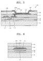
- FIG. 3 is a view of electrode wiring layers of a bottom gate type organic light emitting display device 100 according to one embodiment
- FIG. 4 is a view of a patterned organic semiconductor layer formed on the electrode wiring layers of the bottom gate type organic light emitting display device 100 of FIG. 3
- FIG. 5 is a cross-sectional view of the bottom gate type organic light emitting display device 100 taken along a line V-V of FIG. 3
- FIG. 6 is a cross-sectional view of the bottom gate type organic light emitting display device 100 taken along a line VI-VI of FIG. 3.
- driving TFT M1 includes a first source electrode 111, a first drain electrode 112 and a first gate electrode 113.
- Switching TFT M2 includes a second source electrode 121, a second drain electrode 122 and a second gate electrode 123.
- a data wiring layer 130 constituting a data line DATA is electrically connected to the second source electrode 121.
- a scan wiring layer 140 constituting the scan line SCAN is electrically connected to the second gate electrode 123.
- a driving wiring layer 150 constituting the power supply line Vdd is electrically connected to the first source electrode 111.
- a pixel electrode 160 is electrically connected to the first drain electrode 112.
- a first capacitor layer 171 included in a storage capacitor Cst is connected to the second drain electrode 122 through a contact hole (not shown).
- a second capacitor layer 172 is arranged so as to be electrically connected to the driving wiring layer 150.
- the first source electrode 111, the first drain electrode 112, the second source electrode 121, the second drain electrode 122, the data wiring layer 130, the driving electrode 150, and the second capacitor layer 172 are formed on a gate insulating layer 193.
- the first gate electrode 113, the second gate electrode 123, the scan wiring layer 140, and the first capacitor layer 171 are formed on a buffer layer 192.
- the first source electrode 111, the first drain electrode 112, the second source electrode 121, the second drain electrode 122, the data wiring layer 130, the driving electrode 150, the second capacitor layer 172, the first gate electrode 113, the second gate electrode 123, the scan wiring layer 140, and the first capacitor layer 171 are all electrical conductors.
- an organic semiconductor layer is formed on a gate insulating layer 193. After forming the organic semiconductor layer, the organic semiconductor layer is patterned using a laser ablation (LAT) method.
- LAT laser ablation
- the LAT process in the patterning of the organic semiconductor layer can damage an underlying electrode wiring layer, especially when the organic semiconductor layer is removed off an underlying electrode wiring layer. Therefore, the present embodiment avoids this damage to the electrode wiring layer by only removing portions of the organic semiconductor layer that do not lye on top of the electrode wiring layer.
- FIGS. 5 and 6 each illustrate cross-sectional views of the bottom gate type organic light emitting display device 100 including an organic semiconductor layer 180 after the patterning as described above, according to an embodiment.
- the buffer layer 192 is formed on a substrate 191.
- the first gate electrode 113 is formed on the buffer layer 192.
- the gate insulating layer 193 is formed so as to cover the first gate electrode 113.
- the substrate 191 can be a glass substrate, a plastic substrate or a metal substrate.
- the metal substrate can be formed of metal foil, for example, stainless steel, Ti, Mo, an Invar alloy, an Inconel alloy, a Kovar alloy, or the like.
- the plastic substrate can include a plastic film made out of either polyethersulphone (PES), polyacrylate (PAR), polyetherimide (PEI), polyethyelenen napthalate (PEN), polyethyeleneterepthalate (PET), polyphenylene sulfide (PPS), polyallylate, polyimide, polycarbonate (PC), cellulous triacetate (TAC) or cellulose acetate propinonate (CAP).
- PES polyethersulphone
- PAR polyacrylate
- PEI polyetherimide
- PEN polyethyelenen napthalate
- PET polyethyeleneterepthalate
- PPS polyphenylene sulfide
- PC polycarbonate
- TAC cell
- the buffer layer 192 is formed of an organic compound and/or an inorganic compound, preferably, SiO x (x ⁇ 1) or SiN x (x ⁇ 1).
- the gate insulating layer 193 can be an organic insulating layer, an inorganic insulating layer or an organic-inorganic hybrid layer, and can be formed as a single-layered or multi-layered structure.
- the first source electrode 111 and the first drain electrode 112 are formed on the gate insulating layer 193.
- the organic semiconductor layer 180 is formed using the patterning as described above. Here, the organic semiconductor layer 180 covers the first source electrode 111 and the first drain electrode 112 completely.
- the first source electrode 111, the first drain electrode 112 and the first gate electrode 113 are formed of materials having good electrical conductivity, such as a metal such as Ag, Mg, Al, Pt, Pd, Au, Ni, Nd, Ir, Cr, Li, Ca, a compound thereof, or the like.
- the organic semiconductor layer 180 can be formed of at least one of pentacene, tetracene, anthracene, naphthalene, ⁇ -6-thiophen, perylene and a derivative thereof, rubrene and a derivative thereof, coronene and a derivative thereof, perylene tetracarboxylic diimide and a derivative thereof, perylene tetracarboxylic dianhydride and a derivative thereof, polythiophene and a derivative thereof, polyparaphenylene vinylene and a derivative thereof, polyfluorene and a derivative thereof, polythiophene vynylene and a derivative thereof, polyparaphenylene and a derivative thereof, a polythiophene-heterocyclic aromatic copolymer and a derivative thereof, olignaphthalene and a derivative thereof, oligothiophene of ⁇ -5-thiophene and a derivative thereof, a metal-containing or metal-free phthalocyanine and
- the second capacitor layer 172 is formed on the gate insulating layer 193, wherein the organic semiconductor layer 180 is formed using the patterning as described above to cover the second capacitor layer 172 completely.
- a planarized insulating layer 194 is further formed to cover the organic semiconductor layer 180.
- the pixel electrode 160 is formed on the planarized insulating layer 194 while electrically connecting to the first drain electrode 112 through a contact hole 194a.
- the contact hole 194a can be formed using a laser etching method, a photolithographic method, or the like.
- a pixel definition layer 195 is formed so as to cover the pixel electrode 160.
- a predetermined opening 195a is formed in the pixel definition layer 195.
- the pixel definition layer 195 can be an organic insulating layer, an inorganic insulating layer or an organic-inorganic hybrid layer, and can be formed as a single-layered or a multi-layered structure.
- the organic insulating layer can be formed of polymer materials, for example, a general purpose compound (PMMA, PS), a polymer derivative including a phenol group, a acryl-based polymer, an imide-based polymer, an aryl ether-based, an amide-based polymer, a fluorine-based polymer, a p-xilylene-based polymer, a vinyl alcohol-based polymer, a blend thereof, or the like.
- the inorganic insulating layer can be SiO 2 , SiN x , SiON, Al 2 O 3 , TiO 2 , Ta 2 O 5 , HfO 2 , ZrO 2 , BST, PZT, or the like.
- the pixel definition layer 195 can be formed using an ink jet printing method. First, some parts of the pixel electrode 160 are surface-treated. In cases where the adhesive force between an untreated substrate surface and the ink is good, a fluorine-based plasma is used to make portions of the substrate surface that corresponds to opening 195a water-repellant. Here, fluorine-based gases such as CF 4 or C 3 F 8 are used in the surface treatment with the fluorine-based plasma. The pixel definition layer 195 is then formed by discharging a solution including insulating materials for the pixel definition layer 195 from an inkjet head. The opening 195a exposing the pixel electrode 160 through the pixel definition layer 195 is formed on the surface-treated parts of the pixel electrode 160.
- a fluorine-based plasma is used to make portions of the substrate surface that corresponds to opening 195a water-repellant.
- fluorine-based gases such as CF 4 or C 3 F 8 are used in the surface treatment with the fluorine-based plasma.
- the pixel definition layer 195 can be formed by surface-treating portions of the substrate surface that do not correspond to opening 195a with Ar and O 2 plasmas. That is, by surface-treating the parts of the substrate surface except for the pixel electrode 160 corresponding to the opening 195a using Ar and O 2 plasmas, the substrate surface is hydrophilized to increase the adhesive force.
- the pixel definition layer 195 is coated on only the surface-treated parts having the increased adhesive force.
- the pixel definition layer 195 is not formed on a surface of the pixel electrode 160 which is not surface-treated with plasma. Meanwhile, an organic light emitting layer 196 and an opposite electrode 197 are stacked on the exposed pixel electrode 160 sequentially.
- the opposite electrode 197 is formed to cover all the pixels, but the structure of the opposite electrode 197 is not limited thereto. That is, the opposite electrode 197 can be patterned.
- the opposite electrode 197 is a cathode electrode, or vice versa.
- the pixel electrode 160 is an anode electrode.
- the pixel electrode 160 can be a transparent electrode
- the opposite electrode 197 can be a reflective electrode.
- the transparent electrode has a high work function, and can be formed of transparent ITO, IZO, In 2 O 3 , ZnO, or the like.
- the reflective electrode constituting the opposite electrode 197 is formed of a metal such as Ag, Mg, Al, Pt, Pd, Au, Ni, Nd, Ir, Cr, Li, Ca or a compound thereof having a low work function.
- the pixel electrode 160 can be the reflective electrode, and the opposite electrode 197 can be the transparent electrode.
- the reflective electrode constituting the pixel electrode 160 can be formed by forming a reflective layer with Ag, Mg, Al, Pt, Pd, Au, Ni, Nd, Ir, Cr, Li, Ca, a compound thereof, or the like, and forming ITO, IZO, ZnO, In 2 O 3 or the like having a high work function on the reflective layer.
- the transparent electrode constituting the opposite electrode 197 is formed by depositing Ag, Mg, Al, Pt, Pd, Au, Ni, Nd, Ir, Cr, Li, Ca, a compound thereof, or the like having a low work function, and forming thereon a subsidiary electrode layer or a bus line with transparent materials such as ITO, IZO, ZnO, In 2 O 3 , and the like.
- both the pixel electrode 160 and the opposite electrode 197 can be transparent electrodes.
- the pixel electrode 160 and opposite electrode 197 can be formed of electrically conductive materials, conductive pastes including conductive particles such as Ag, Mg, Cu, etc., or the like.
- the conductive pastes can be printed using an ink jet printing method. After printing, the conductive pastes are sintered to form the pixel electrode 160 and the opposite electrode 197.
- the organic light emitting layer 196 can be a small molecular weight organic layer or a polymer organic layer.
- a Hole Injection Layer (HIL), a Hole Transport Layer (HTL), an Emission Layer (EML), an Electron Transport Layer (ETL), an Electron Injection Layer (EIL), or the like are stacked to have a single or multi-layer structure.
- the organic light emitting layer 196 can be formed of organic materials such as copper phthalocyanine (CuPc), N,N'-di(naphthalene-1-yl)-N,N'-diphenyl-benzidine (NPB), tris-8-hydroxyquinoline aluminum (Alq 3 ), or the like, but materials for forming the organic light emitting layer 196 are not limited thereto.
- the small molecular weight organic layer can be formed using a vapor deposition method.
- the polymer organic layer can generally include a HTL and an EML.
- the HTL can be formed of PEDOT.
- the EML can be formed of polymer organic materials such as Poly-Phenylenevinylene (PPV)-based materials, Polyfluorene-based materials, or the like using a screen printing method, an ink jet printing method, or the like.
- PPV Poly-Phenylenevinylene
- the bottom gate type organic light emitting display device 100 After the bottom gate type organic light emitting display device 100 is formed, an upper part thereof is sealed to provide protection from the atmospheric.
- the electrode wiring layers are not damaged during the patterning of the organic semiconductor layer 180.
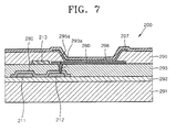
- FIG. 7 is a schematic cross-sectional view of an organic light emitting display device 200 according to another embodiment.
- the organic light emitting display device 200 is a top gate type organic light emitting display device.
- the structure of the top gate type organic light emitting display device 200 is described as follows with reference to FIG. 7.
- a buffer layer 292 is formed on a substrate 291.
- a first source electrode 211 and a first drain electrode 212 are formed on the buffer layer 292.
- a second source electrode, a second drain electrode, a data wiring layer, a driving wiring layer, and a second capacitor layer can also be formed on the buffer layer 292.
- the organic semiconductor layer 280 is patterned using a LAT method.
- the organic semiconductor layer 280 is patterned so that the patterned organic semiconductor layer completely covers each of the first source electrode 211 and the first drain electrode 212.
- the organic semiconductor layer 280 is patterned so as to completely cover other electrode wiring layers formed on the buffer layer 292, such as a second source electrode, a second drain electrode, a data wiring layer, a driving wiring layer, and a second capacitor layer.
- parts of the organic semiconductor layer to be removed are parts of the organic semiconductor layer not covering an electrode wiring layer formed on the buffer layer 292.
- a gate insulating layer 293 is further formed so as to cover the organic semiconductor layer 280, and a first gate electrode 213 and a pixel electrode 260 are formed on the gate insulating layer 293.
- a second gated electrode, a scan wiring layer, and a first capacitor layer are also formed on the gate insulating layer 293.
- a pixel definition layer 295 is formed on the gate insulating layer 293.
- An additional contact hole 293a is formed in the gate insulating layer 293 and the organic semiconductor layer 280 to electrically connect the pixel electrode 260 and the first drain electrode 212.
- An organic light emitting layer 296 and an opposite electrode 297 are stacked on the exposed pixel electrode 260 sequentially. After forming the top gate type organic light emitting display device 200, an upper part of the organic light emitting display device 200 is sealed to provide protection from the atmosphere.
- the structures of the first source electrode 211, the first drain electrode 212, the first gate electrode 213, the pixel electrode 260, the organic semiconductor layer 280, the substrate 291, the buffer layer 292, the gate insulating layer 293, the pixel definition layer 295, the organic light emitting layer 296, and the opposite electrode 297 illustrated in FIG. 7 are equivalent to the first source electrode 111, the first drain electrode 112, the first gate electrode 113, the pixel electrode 160, the organic semiconductor layer 180, the substrate 191, the buffer layer 192, the gate insulating layer 193, the pixel definition layer 195, the organic light emitting layer 1296, and the opposite electrode 197 of the organic light emitting display device 100 respectively, and thus detailed descriptions thereof has been omitted.
- the electrode wiring layers are not damaged during patterning of the organic semiconductor layer 280.
- the organic light emitting display device 200 As the structure, operation, and effect of the organic light emitting display device 200 other than described herein are the same as the structure, operation, and effect of the organic light emitting display device 100 illustrated in FIGS. 1 through 6, a detailed descriptions thereof has been omitted.
Abstract
Description
- The present invention relates to an organic thin film transistor (OTFT) having a patterned organic semiconductor layer designed to prevent damage to an underlying electrode wiring layer formed, and an organic light emitting display device including the OTFT.
- Active matrix (AM) organic light emitting display devices include a pixel circuit for each pixel. A pixel circuit is electrically connected to a scan line, a data line, and a power supply line and includes a thin film transistor (TFT) and a storage capacitor. Organic thin film transistors (OTFTs) use an organic layer as a semiconductor layer instead of using a silicon layer. OTFTs can operate at a low temperature and can be used as driving devices, and thus have been actively researched as possible switching elements of flexible organic light emitting display devices.
- An organic light emitting display device that uses OTFTs as switching devices includes an organic semiconductor layer and a plurality of electrode wiring layers. When patterning the organic semiconductor layer, sometimes the underlying electrode wiring layers can be damaged. In particular, when patterning, sometimes source and drain electrodes of OTFTs can be damaged.
- OTFTs include an organic semiconductor layer formed on the source and drain electrodes. In OTFTs, the organic semiconductor layer covers a portion of the source and drain electrodes because the organic semiconductor layer is patterned to form only a channel and not to completely cover the source and drain electrodes. Accordingly, when patterning an organic semiconductor layer of an OTFT, the organic semiconductor layer is blanket formed, and then parts of the organic semiconductor layer that will not become part of the channel are removed using a laser, etc. Since the source and drain electrodes and other electrode wiring layers can be damaged during this removal of the organic semiconductor layer, the OTFT can be defective. Wherefore, what is needed is a design for a design for an OTFT and a design for a display using the same that does not result in a damaged electrode layer.
- Accordingly, a first aspect of the present invention provides an organic thin film transistor as defined in the attached Claim 1. Preferred features are defined in the attached dependent Claims 2 to 6.
- In a further aspect of the present invention there is provided an organic light emitting display device as defined in the attached Claim 7. Preferred features are defined in the attached dependent Claims 8 to 12.
- A more complete appreciation of the invention, and many of the attendant advantages thereof, will be readily apparent as the same becomes better understood by reference to the following detailed description when considered in conjunction with the accompanying drawings in which like reference symbols indicate same or similar components, wherein:
- FIG. 1 is a view of a circuit diagram of a pixel circuit (PC) used in an organic light emitting display device according to an embodiment of the present invention;
- FIG. 2 is a detailed view of a circuit diagram of the PC of FIG. 1;
- FIG. 3 is a view of electrode wiring layers of a bottom gate type organic light emitting display device according to an embodiment of the present invention;
- FIG. 4 is a view of a patterned organic semiconductor layer formed on the electrode wiring layers of the bottom gate type organic light emitting display device of FIG. 3;
- FIG. 5 is a cross-sectional view of the bottom gate type organic light emitting display device taken along line V-V of FIG. 3;
- FIG. 6 is a cross-sectional view of the bottom gate type organic light emitting display device taken along line VI-VI of FIG. 3; and
- FIG. 7 is a schematic cross-sectional view of a top gate type organic light emitting display device according to another embodiment of the present invention.
- Turning now to the figures, FIG. 1 is a view of a circuit diagram of a pixel circuit (PC) used in an organic light emitting display device according to embodiment of the present invention. As illustrated in FIG. 1, each of a plurality of pixels in the organic light emitting display device includes a data line DATA, a scan line SCAN and an organic light-emitting element and a power supply line Vdd that supplies power to the OLED. The PC of each pixel is electrically connected to the data line DATA, the scan line SCAN and the power supply line Vdd and controls the light emission of the OLED.
- Turning now to FIG. 2, FIG. 2 is a detailed view of a detailed circuit diagram of the PC of FIG. 1. The PC includes a driving TFT M1, a switching TFT M2, and a single storage capacitor Cst. Referring to FIG. 2, each pixel of the organic light-emitting display device according to the present embodiment includes at least two thin film transistors, namely, the switching TFT M2 and the driving TFT M1, the storage capacitor Cst, and the OLED.
- The switching TFT M2 is turned on/off by a scan signal received by the scan line SCAN and delivers a data signal from the data line DATA to the storage capacitor Cst and the driving TFT M1. Further embodiments are not limited to the case in which the switching TFT M2 is a single TFT as illustrated in FIG. 2. In another embodiment, a switching device can include a plurality of TFTs and a capacitor. The pixel of FIG. 2 can further include a circuit which compensates for the Vth value of the driving TFT M1 or a circuit which compensates for the voltage drop in the power supply line Vdd.
- The driving TFT M1 determines the amount of current flowing into the OLED according to the data signal received through the switching TFT M2. The storage capacitor Cst stores the data signal received through the switching TFT M2 for one frame.
- Although the driving TFT M1 and the switching TFT M2 are illustrated as PMOS TFTs in FIG. 2, further embodiments are not limited thereto. At least one of the driving TFT M1 and the switching TFT M2 can be implemented as an NMOS TFT. In addition, the number of TFTs and the number of capacitors are not limited to those illustrated in FIG. 2. In other words, a greater number of TFTs and a greater number of capacitors than those illustrated in FIG. 2 can be included.
- Turning now to FIGS. 3 through 6, FIG. 3 is a view of electrode wiring layers of a bottom gate type organic light
emitting display device 100 according to one embodiment, FIG. 4 is a view of a patterned organic semiconductor layer formed on the electrode wiring layers of the bottom gate type organic lightemitting display device 100 of FIG. 3, FIG. 5 is a cross-sectional view of the bottom gate type organic lightemitting display device 100 taken along a line V-V of FIG. 3, and FIG. 6 is a cross-sectional view of the bottom gate type organic lightemitting display device 100 taken along a line VI-VI of FIG. 3. - Referring now to FIG. 3, driving TFT M1 includes a
first source electrode 111, afirst drain electrode 112 and afirst gate electrode 113. Switching TFT M2 includes asecond source electrode 121, asecond drain electrode 122 and asecond gate electrode 123. Adata wiring layer 130 constituting a data line DATA is electrically connected to thesecond source electrode 121. Ascan wiring layer 140 constituting the scan line SCAN is electrically connected to thesecond gate electrode 123. Adriving wiring layer 150 constituting the power supply line Vdd is electrically connected to thefirst source electrode 111. Apixel electrode 160 is electrically connected to thefirst drain electrode 112. In addition, afirst capacitor layer 171 included in a storage capacitor Cst is connected to thesecond drain electrode 122 through a contact hole (not shown). Asecond capacitor layer 172 is arranged so as to be electrically connected to thedriving wiring layer 150. - Here, the
first source electrode 111, thefirst drain electrode 112, thesecond source electrode 121, thesecond drain electrode 122, thedata wiring layer 130, thedriving electrode 150, and thesecond capacitor layer 172 are formed on agate insulating layer 193. Thefirst gate electrode 113, thesecond gate electrode 123, thescan wiring layer 140, and thefirst capacitor layer 171 are formed on abuffer layer 192. Thefirst source electrode 111, thefirst drain electrode 112, thesecond source electrode 121, thesecond drain electrode 122, thedata wiring layer 130, thedriving electrode 150, thesecond capacitor layer 172, thefirst gate electrode 113, thesecond gate electrode 123, thescan wiring layer 140, and thefirst capacitor layer 171 are all electrical conductors. - After each of the electrodes are formed, an organic semiconductor layer is formed on a
gate insulating layer 193. After forming the organic semiconductor layer, the organic semiconductor layer is patterned using a laser ablation (LAT) method. - When the organic semiconductor layer is patterned, parts of the organic semiconductor layer to be removed are denoted by the shaded area (P) of FIG. 4. By doing so, no metal is exposed so that there is no removal of any of the organic semiconductor layer that covers the electrode wiring layer. Specifically, each of the
first source electrode 111, thefirst drain electrode 112, thesecond source electrode 121, thesecond drain electrode 122, thedata wiring layer 130, thedriving wiring layer 150, and thesecond capacitor layer 172 formed on thegate insulating layer 193 are still totally covered with the organic semiconductor layer, even after the patterning of the organic semiconductor layer. - It is to be appreciated that the LAT process in the patterning of the organic semiconductor layer can damage an underlying electrode wiring layer, especially when the organic semiconductor layer is removed off an underlying electrode wiring layer. Therefore, the present embodiment avoids this damage to the electrode wiring layer by only removing portions of the organic semiconductor layer that do not lye on top of the electrode wiring layer.
- Turning now to FIGS. 5 and 6, FIGS. 5 and 6 each illustrate cross-sectional views of the bottom gate type organic light
emitting display device 100 including anorganic semiconductor layer 180 after the patterning as described above, according to an embodiment. Referring to FIG. 5, thebuffer layer 192 is formed on asubstrate 191. Thefirst gate electrode 113 is formed on thebuffer layer 192. After forming thefirst gate electrode 113, thegate insulating layer 193 is formed so as to cover thefirst gate electrode 113. - Here, the
substrate 191 can be a glass substrate, a plastic substrate or a metal substrate. The metal substrate can be formed of metal foil, for example, stainless steel, Ti, Mo, an Invar alloy, an Inconel alloy, a Kovar alloy, or the like. The plastic substrate can include a plastic film made out of either polyethersulphone (PES), polyacrylate (PAR), polyetherimide (PEI), polyethyelenen napthalate (PEN), polyethyeleneterepthalate (PET), polyphenylene sulfide (PPS), polyallylate, polyimide, polycarbonate (PC), cellulous triacetate (TAC) or cellulose acetate propinonate (CAP). - The
buffer layer 192 is formed of an organic compound and/or an inorganic compound, preferably, SiOx (x≥1) or SiNx (x≥1). Thegate insulating layer 193 can be an organic insulating layer, an inorganic insulating layer or an organic-inorganic hybrid layer, and can be formed as a single-layered or multi-layered structure. - Meanwhile, after forming the
gate insulating layer 193, thefirst source electrode 111 and thefirst drain electrode 112 are formed on thegate insulating layer 193. Theorganic semiconductor layer 180 is formed using the patterning as described above. Here, theorganic semiconductor layer 180 covers thefirst source electrode 111 and thefirst drain electrode 112 completely. - The
first source electrode 111, thefirst drain electrode 112 and thefirst gate electrode 113 are formed of materials having good electrical conductivity, such as a metal such as Ag, Mg, Al, Pt, Pd, Au, Ni, Nd, Ir, Cr, Li, Ca, a compound thereof, or the like. - The
organic semiconductor layer 180 can be formed of at least one of pentacene, tetracene, anthracene, naphthalene, α-6-thiophen, perylene and a derivative thereof, rubrene and a derivative thereof, coronene and a derivative thereof, perylene tetracarboxylic diimide and a derivative thereof, perylene tetracarboxylic dianhydride and a derivative thereof, polythiophene and a derivative thereof, polyparaphenylene vinylene and a derivative thereof, polyfluorene and a derivative thereof, polythiophene vynylene and a derivative thereof, polyparaphenylene and a derivative thereof, a polythiophene-heterocyclic aromatic copolymer and a derivative thereof, olignaphthalene and a derivative thereof, oligothiophene of α-5-thiophene and a derivative thereof, a metal-containing or metal-free phthalocyanine and a derivative thereof, pyromellitic dianhydride and a derivative thereof, pyromellitic diimide and a derivative thereof, perylene tetracarboxylic acid dianhydride and a derivative thereof, naphthalene tetracarboxylic acid diimide and a derivative thereof, naphthalene perylene tetracarboxylic acid dianhydride and a derivative thereof. - Referring now to FIG. 6, the
second capacitor layer 172 is formed on thegate insulating layer 193, wherein theorganic semiconductor layer 180 is formed using the patterning as described above to cover thesecond capacitor layer 172 completely. A planarized insulatinglayer 194 is further formed to cover theorganic semiconductor layer 180. Thepixel electrode 160 is formed on the planarized insulatinglayer 194 while electrically connecting to thefirst drain electrode 112 through acontact hole 194a. Thecontact hole 194a can be formed using a laser etching method, a photolithographic method, or the like. - After forming the
pixel electrode 160, apixel definition layer 195 is formed so as to cover thepixel electrode 160. Apredetermined opening 195a is formed in thepixel definition layer 195. Thepixel definition layer 195 can be an organic insulating layer, an inorganic insulating layer or an organic-inorganic hybrid layer, and can be formed as a single-layered or a multi-layered structure. - The organic insulating layer can be formed of polymer materials, for example, a general purpose compound (PMMA, PS), a polymer derivative including a phenol group, a acryl-based polymer, an imide-based polymer, an aryl ether-based, an amide-based polymer, a fluorine-based polymer, a p-xilylene-based polymer, a vinyl alcohol-based polymer, a blend thereof, or the like. The inorganic insulating layer can be SiO2, SiNx, SiON, Al2O3, TiO2, Ta2O5, HfO2, ZrO2, BST, PZT, or the like.
- The
pixel definition layer 195 can be formed using an ink jet printing method. First, some parts of thepixel electrode 160 are surface-treated. In cases where the adhesive force between an untreated substrate surface and the ink is good, a fluorine-based plasma is used to make portions of the substrate surface that corresponds to opening 195a water-repellant. Here, fluorine-based gases such as CF4 or C3F8 are used in the surface treatment with the fluorine-based plasma. Thepixel definition layer 195 is then formed by discharging a solution including insulating materials for thepixel definition layer 195 from an inkjet head. Theopening 195a exposing thepixel electrode 160 through thepixel definition layer 195 is formed on the surface-treated parts of thepixel electrode 160. - In cases where the adhesive force between the untreated substrate surface and an ink is poor, that is, the substrate surface is water-repellant, the
pixel definition layer 195 can be formed by surface-treating portions of the substrate surface that do not correspond to opening 195a with Ar and O2 plasmas. That is, by surface-treating the parts of the substrate surface except for thepixel electrode 160 corresponding to theopening 195a using Ar and O2 plasmas, the substrate surface is hydrophilized to increase the adhesive force. Next, when ink including insulating materials for forming thepixel definition layer 195 is discharged on the substrate surface, thepixel definition layer 195 is coated on only the surface-treated parts having the increased adhesive force. Accordingly, thepixel definition layer 195 is not formed on a surface of thepixel electrode 160 which is not surface-treated with plasma. Meanwhile, an organiclight emitting layer 196 and anopposite electrode 197 are stacked on the exposedpixel electrode 160 sequentially. Here, theopposite electrode 197 is formed to cover all the pixels, but the structure of theopposite electrode 197 is not limited thereto. That is, theopposite electrode 197 can be patterned. - When the
pixel electrode 160 is an anode electrode, theopposite electrode 197 is a cathode electrode, or vice versa. In the current embodiment, thepixel electrode 160 is an anode electrode. - When the organic light emitting
display device 100 is a bottom emission type organic light emitting display device, thepixel electrode 160 can be a transparent electrode, and theopposite electrode 197 can be a reflective electrode. Here, the transparent electrode has a high work function, and can be formed of transparent ITO, IZO, In2O3, ZnO, or the like. The reflective electrode constituting theopposite electrode 197 is formed of a metal such as Ag, Mg, Al, Pt, Pd, Au, Ni, Nd, Ir, Cr, Li, Ca or a compound thereof having a low work function. - When the organic light emitting
display device 100 is a top emission type organic light emitting display device, thepixel electrode 160 can be the reflective electrode, and theopposite electrode 197 can be the transparent electrode. Here, the reflective electrode constituting thepixel electrode 160 can be formed by forming a reflective layer with Ag, Mg, Al, Pt, Pd, Au, Ni, Nd, Ir, Cr, Li, Ca, a compound thereof, or the like, and forming ITO, IZO, ZnO, In2O3 or the like having a high work function on the reflective layer. The transparent electrode constituting theopposite electrode 197 is formed by depositing Ag, Mg, Al, Pt, Pd, Au, Ni, Nd, Ir, Cr, Li, Ca, a compound thereof, or the like having a low work function, and forming thereon a subsidiary electrode layer or a bus line with transparent materials such as ITO, IZO, ZnO, In2O3, and the like. - When the organic light emitting
display device 100 is a dual emission type organic light emitting display device, both thepixel electrode 160 and theopposite electrode 197 can be transparent electrodes. - Materials for forming the
pixel electrode 160 andopposite electrode 197 are not limited to the materials described above, that is, thepixel electrode 160 andopposite electrode 197 can be formed of electrically conductive materials, conductive pastes including conductive particles such as Ag, Mg, Cu, etc., or the like. When thepixel electrode 160 and theopposite electrode 197 are formed of conductive pastes, the conductive pastes can be printed using an ink jet printing method. After printing, the conductive pastes are sintered to form thepixel electrode 160 and theopposite electrode 197. - The organic
light emitting layer 196 can be a small molecular weight organic layer or a polymer organic layer. When the organiclight emitting layer 196 is a small molecular weight organic layer, a Hole Injection Layer (HIL), a Hole Transport Layer (HTL), an Emission Layer (EML), an Electron Transport Layer (ETL), an Electron Injection Layer (EIL), or the like are stacked to have a single or multi-layer structure. The organiclight emitting layer 196 can be formed of organic materials such as copper phthalocyanine (CuPc), N,N'-di(naphthalene-1-yl)-N,N'-diphenyl-benzidine (NPB), tris-8-hydroxyquinoline aluminum (Alq3), or the like, but materials for forming the organiclight emitting layer 196 are not limited thereto. The small molecular weight organic layer can be formed using a vapor deposition method. - The polymer organic layer can generally include a HTL and an EML. Here, the HTL can be formed of PEDOT. The EML can be formed of polymer organic materials such as Poly-Phenylenevinylene (PPV)-based materials, Polyfluorene-based materials, or the like using a screen printing method, an ink jet printing method, or the like.
- After the bottom gate type organic light emitting
display device 100 is formed, an upper part thereof is sealed to provide protection from the atmospheric. - According to the current embodiment, by patterning the
organic semiconductor layer 180 so as to completely cover the electrode wiring layers formed on thegate insulating layer 193, that is thefirst source electrode 111, thefirst drain electrode 112, thesecond source electrode 121, thesecond drain electrode 122, thedata wiring layer 130, the drivingwiring layer 150, and thesecond capacitor layer 172, the electrode wiring layers are not damaged during the patterning of theorganic semiconductor layer 180. - Turning now to FIG. 7, FIG. 7 is a schematic cross-sectional view of an organic light emitting
display device 200 according to another embodiment. The organic light emittingdisplay device 200 is a top gate type organic light emitting display device. The structure of the top gate type organic light emittingdisplay device 200 is described as follows with reference to FIG. 7. - First, a
buffer layer 292 is formed on asubstrate 291. Afirst source electrode 211 and afirst drain electrode 212 are formed on thebuffer layer 292. Although not illustrated in FIG. 7, a second source electrode, a second drain electrode, a data wiring layer, a driving wiring layer, and a second capacitor layer can also be formed on thebuffer layer 292. - After forming an
organic semiconductor layer 280 similar to theorganic layer 180 of the bottom gate type organic light emittingdisplay device 100, theorganic semiconductor layer 280 is patterned using a LAT method. Theorganic semiconductor layer 280 is patterned so that the patterned organic semiconductor layer completely covers each of thefirst source electrode 211 and thefirst drain electrode 212. Although not illustrated in FIG. 7, theorganic semiconductor layer 280 is patterned so as to completely cover other electrode wiring layers formed on thebuffer layer 292, such as a second source electrode, a second drain electrode, a data wiring layer, a driving wiring layer, and a second capacitor layer. - When the top gate type organic light emitting
display device 200 is patterned using the LAT method, since some parts of theorganic semiconductor layer 280 and electrodes under theorganic semiconductor layer 280 can be damaged, parts of the organic semiconductor layer to be removed are parts of the organic semiconductor layer not covering an electrode wiring layer formed on thebuffer layer 292. - Next, a
gate insulating layer 293 is further formed so as to cover theorganic semiconductor layer 280, and afirst gate electrode 213 and apixel electrode 260 are formed on thegate insulating layer 293. Although not illustrated in FIG. 7, a second gated electrode, a scan wiring layer, and a first capacitor layer are also formed on thegate insulating layer 293. - After forming the
first gate electrode 213, thepixel electrode 260, etc. on thegate insulating layer 293, apixel definition layer 295, through which anopening 295a is formed, is formed on thegate insulating layer 293. Anadditional contact hole 293a is formed in thegate insulating layer 293 and theorganic semiconductor layer 280 to electrically connect thepixel electrode 260 and thefirst drain electrode 212. - An organic
light emitting layer 296 and anopposite electrode 297 are stacked on the exposedpixel electrode 260 sequentially. After forming the top gate type organic light emittingdisplay device 200, an upper part of the organic light emittingdisplay device 200 is sealed to provide protection from the atmosphere. - The structures of the
first source electrode 211, thefirst drain electrode 212, thefirst gate electrode 213, thepixel electrode 260, theorganic semiconductor layer 280, thesubstrate 291, thebuffer layer 292, thegate insulating layer 293, thepixel definition layer 295, the organiclight emitting layer 296, and theopposite electrode 297 illustrated in FIG. 7 are equivalent to thefirst source electrode 111, thefirst drain electrode 112, thefirst gate electrode 113, thepixel electrode 160, theorganic semiconductor layer 180, thesubstrate 191, thebuffer layer 192, thegate insulating layer 193, thepixel definition layer 195, the organic light emitting layer 1296, and theopposite electrode 197 of the organic light emittingdisplay device 100 respectively, and thus detailed descriptions thereof has been omitted. - According to the current embodiment, by patterning the
organic semiconductor layer 280 so as to completely cover all the electrode wiring layers formed on thebuffer layer 292, that is thefirst source electrode 211, thefirst drain electrode 212, the second source electrode, the second drain electrode, the data wiring layer, the driving wiring layer, and the second capacitor, the electrode wiring layers are not damaged during patterning of theorganic semiconductor layer 280. - As the structure, operation, and effect of the organic light emitting
display device 200 other than described herein are the same as the structure, operation, and effect of the organic light emittingdisplay device 100 illustrated in FIGS. 1 through 6, a detailed descriptions thereof has been omitted. - Although the above-described embodiments apply to an organic light emitting display device, further embodiments apply to various kinds of flat display devices such as liquid crystal display devices, etc. in which an organic semiconductor layer can be used. As described above, by applying a patterned organic semiconductor layer for protecting electrode wiring layers formed before the organic semiconductor layer is patterned, the electrode wiring layers can be protected, and the quality of product can be improved.
- While the present invention has been particularly shown and described with reference to exemplary embodiments thereof, it will be understood by those of ordinary skill in the art that various changes in form and details can be made therein without departing from the scope of the present invention as defined by the following claims.
Claims (12)
- An organic thin film transistor, OTFT, comprising:a gate electrode;a source electrode and a drain electrode insulated from the gate electrode; andan organic semiconductor layer insulated from the gate electrode and in contact with the source and drain electrodes, wherein the organic semiconductor layer covers each of the source and drain electrodes.
- An organic thin film transistor according to claim 1, wherein the source and drain electrodes are insulated from the gate electrode by a gate insulating layer.
- An organic thin film transistor according to claim 1 or 2, wherein the organic semiconductor layer comprises a material selected from the group consisting of pentacene, tetracene, anthracene, naphthalene, α-6-thiophen, perylene and a derivative thereof, rubrene and a derivative thereof, coronene and a derivative thereof, perylene tetracarboxylic diimide and a derivative thereof, perylene tetracarboxylic dianhydride and a derivative thereof, polythiophene and a derivative thereof, polyparaphenylene vinylene and a derivative thereof, polyfluorene and a derivative thereof, polythiophene vynylene and a derivative thereof, polyparaphenylene and a derivative thereof, a polythiophene-heterocyclic aromatic copolymer and a derivative thereof, oligoacence of naphthalene and a derivative thereof, oligothiophene of α-5-thiophene and a derivative thereof, a metal-containing or metal-free phthalocyanine and a derivative thereof, pyromellitic dianhydride and a derivative thereof, pyromellitic diimide and a derivative thereof, perylene tetracarboxylic acid dianhydride and a derivative thereof, naphthalene tetracarboxylic acid diimide and a derivative thereof, naphthalene tetracarboxylic acid dianhydride and a derivative thereof.
- An organic thin film transistor according to any preceding claim, wherein the organic semiconductor layer completely covers each of the source electrode and the drain electrode.
- An organic thin film transistor according to any preceding claim, further comprising a wiring layer connected to the source and drain electrodes.
- An organic thin film transistor according to claim 5, wherein the organic semiconductor layer completely covers the wiring layer.
- An organic light emitting display device, comprising:a substrate;an electrical conductor arranged on the substrate;an organic semiconductor layer covering the electrical conductor; andan organic light-emitting element electrically connected to the electrical conductor.
- An organic light emitting display device according to claim 7, further comprising a pixel circuit electrically connected to the organic light-emitting element,
wherein the electrical conductor is at least one electrode wiring of the pixel circuit. - An organic light emitting display device according to claim 8, wherein the pixel circuit comprises an organic thin film transistor, a capacitor, a data wiring layer, a scan wiring layer and a driving wiring layer.
- An organic light emitting display device according to claim 9, wherein the organic thin film transistor comprises a gate electrode, and source and drain electrodes insulated from the gate electrode.
- An organic light emitting display device according to any one of claims 7 to 10, wherein the organic semiconductor layer comprises a material selected from the group consisting of pentacene, tetracene, anthracene, naphthalene, α-6-thiophen, perylene and a derivative thereof, rubrene and a derivative thereof, coronene and a derivative thereof, perylene tetracarboxylic diimide and a derivative thereof, perylene tetracarboxylic dianhydride and a derivative thereof, polythiophene and a derivative thereof, polyparaphenylene vinylene and a derivative thereof, polyfluorene and a derivative thereof, polythiophene vynylene and a derivative thereof, polyparaphenylene and a derivative thereof, a polythiophene-heterocyclic aromatic copolymer and a derivative thereof, oligoacence of naphthalene and a derivative thereof, oligothiophene of α-5-thiophene and a derivative thereof, a metal-containing or metal-free phthalocyanine and a derivative thereof, pyromellitic dianhydride and a derivative thereof, pyromellitic diimide and a derivative thereof, perylene tetracarboxylic acid dianhydride and a derivative thereof, naphthalene tetracarboxylic acid diimide and a derivative thereof, naphthalene tetracarboxylic acid dianhydride and a derivative thereof.
- An organic light emitting display device according to any one of claims 7 to 11, wherein the organic semiconductor layer completely covers the electrical conductor.
Applications Claiming Priority (1)
| Application Number | Priority Date | Filing Date | Title |
|---|---|---|---|
| KR1020060000156A KR100768199B1 (en) | 2006-01-02 | 2006-01-02 | Organic thin film transistor and organic light emitting display device comprising the same |
Publications (2)
| Publication Number | Publication Date |
|---|---|
| EP1804307A2 true EP1804307A2 (en) | 2007-07-04 |
| EP1804307A3 EP1804307A3 (en) | 2012-02-15 |
Family
ID=37891456
Family Applications (1)
| Application Number | Title | Priority Date | Filing Date |
|---|---|---|---|
| EP07250001A Withdrawn EP1804307A3 (en) | 2006-01-02 | 2007-01-02 | Organic thin film transistor and organic light emitting display device including the same |
Country Status (5)
| Country | Link |
|---|---|
| US (1) | US7687802B2 (en) |
| EP (1) | EP1804307A3 (en) |
| JP (1) | JP4742021B2 (en) |
| KR (1) | KR100768199B1 (en) |
| CN (1) | CN1996637B (en) |
Cited By (3)
| Publication number | Priority date | Publication date | Assignee | Title |
|---|---|---|---|---|
| DE102009007947A1 (en) * | 2009-02-06 | 2010-08-19 | Universität Stuttgart | Process for producing an active matrix OLED display |
| EP2312562A1 (en) * | 2008-07-30 | 2011-04-20 | Sumitomo Chemical Company, Limited | Display device and display device manufacturing method |
| EP2015379A3 (en) * | 2007-07-11 | 2011-05-11 | Ricoh Company, Ltd. | Organic transistor, organic transistor array, and display apparatus |
Families Citing this family (19)
| Publication number | Priority date | Publication date | Assignee | Title |
|---|---|---|---|---|
| KR20090037725A (en) * | 2007-10-12 | 2009-04-16 | 삼성전자주식회사 | Thin film transistor array panel, method for manufacturing the same and display appratus with the same |
| JP2010040897A (en) * | 2008-08-07 | 2010-02-18 | Sony Corp | Organic thin film transistor, production method thereof, and electronic device |
| KR101534009B1 (en) * | 2008-10-21 | 2015-07-07 | 삼성디스플레이 주식회사 | Thin film transistor substrate, method of manufacturing the same, and display apparatus having the same |
| FR2945669B1 (en) * | 2009-05-14 | 2011-12-30 | Commissariat Energie Atomique | ORGANIC FIELD EFFECT TRANSISTOR |
| KR20230165355A (en) | 2009-09-16 | 2023-12-05 | 가부시키가이샤 한도오따이 에네루기 켄큐쇼 | Display device |
| KR101082254B1 (en) * | 2009-11-04 | 2011-11-09 | 삼성모바일디스플레이주식회사 | Organic light emitting display device and method of manufacturing the same |
| CN106098788B (en) * | 2010-04-02 | 2020-10-16 | 株式会社半导体能源研究所 | Semiconductor device with a plurality of semiconductor chips |
| KR101207209B1 (en) * | 2011-02-07 | 2012-12-03 | 성균관대학교산학협력단 | Method for forming thin film encapsulation multilayer and method for fabricating flexible organic semiconductor device |
| KR101804360B1 (en) * | 2011-03-21 | 2017-12-05 | 삼성디스플레이 주식회사 | Organic light emitting display apparatus |
| JP6033071B2 (en) * | 2011-12-23 | 2016-11-30 | 株式会社半導体エネルギー研究所 | Semiconductor device |
| TWI455384B (en) * | 2012-03-01 | 2014-10-01 | Everlight Chem Ind Corp | Flexible organic thin film transistor |
| US9059427B2 (en) * | 2012-09-11 | 2015-06-16 | Apple Inc. | Device and method for top emitting AMOLED |
| JP6277625B2 (en) * | 2013-08-08 | 2018-02-14 | 大日本印刷株式会社 | Organic semiconductor device and manufacturing method thereof |
| JP6160361B2 (en) * | 2013-08-20 | 2017-07-12 | 大日本印刷株式会社 | Organic semiconductor device and manufacturing method thereof |
| JP6435651B2 (en) * | 2014-06-12 | 2018-12-12 | 大日本印刷株式会社 | Organic semiconductor device |
| CN108062932B (en) | 2017-12-20 | 2020-05-26 | 北京航空航天大学 | Pixel circuit with organic thin film transistor structure |
| KR102655343B1 (en) * | 2018-11-15 | 2024-04-04 | 엘지디스플레이 주식회사 | Display device and method of manufacturing the same |
| KR20210149957A (en) * | 2020-06-02 | 2021-12-10 | 삼성디스플레이 주식회사 | Display device and manufacturing method thereof |
| TWI756922B (en) * | 2020-11-17 | 2022-03-01 | 友達光電股份有限公司 | Organic semiconductor device |
Family Cites Families (9)
| Publication number | Priority date | Publication date | Assignee | Title |
|---|---|---|---|---|
| JP3850005B2 (en) | 1999-03-03 | 2006-11-29 | パイオニア株式会社 | Switching element and organic electroluminescence element display device |
| WO2001047044A2 (en) * | 1999-12-21 | 2001-06-28 | Plastic Logic Limited | Forming interconnects |
| SG114502A1 (en) * | 2000-10-24 | 2005-09-28 | Semiconductor Energy Lab | Light emitting device and method of driving the same |
| JP2004062161A (en) * | 2002-06-07 | 2004-02-26 | Seiko Epson Corp | Electro-optical device, its driving method and scanning line selecting method, and electronic equipment |
| JP2004241528A (en) * | 2003-02-05 | 2004-08-26 | Ricoh Co Ltd | Organic semiconductor device and display element having it |
| JP4325479B2 (en) * | 2003-07-17 | 2009-09-02 | セイコーエプソン株式会社 | Organic transistor manufacturing method, active matrix device manufacturing method, display device manufacturing method, and electronic device manufacturing method |
| JP4415653B2 (en) | 2003-11-19 | 2010-02-17 | セイコーエプソン株式会社 | Thin film transistor manufacturing method |
| KR100603349B1 (en) * | 2004-06-17 | 2006-07-20 | 삼성에스디아이 주식회사 | A thin film transistor, a method for manufacturing the same, and a flat panel display device having the same |
| KR100659054B1 (en) * | 2004-06-23 | 2006-12-21 | 삼성에스디아이 주식회사 | Active matrix type organic electroluminescence display device with organic thin film transistor and method of manufacturing the same |
-
2006
- 2006-01-02 KR KR1020060000156A patent/KR100768199B1/en not_active IP Right Cessation
- 2006-12-13 JP JP2006335718A patent/JP4742021B2/en not_active Expired - Fee Related
- 2006-12-28 US US11/646,493 patent/US7687802B2/en active Active
-
2007
- 2007-01-02 EP EP07250001A patent/EP1804307A3/en not_active Withdrawn
- 2007-01-02 CN CN2007100018611A patent/CN1996637B/en not_active Expired - Fee Related
Non-Patent Citations (1)
| Title |
|---|
| None * |
Cited By (6)
| Publication number | Priority date | Publication date | Assignee | Title |
|---|---|---|---|---|
| EP2015379A3 (en) * | 2007-07-11 | 2011-05-11 | Ricoh Company, Ltd. | Organic transistor, organic transistor array, and display apparatus |
| EP2312562A1 (en) * | 2008-07-30 | 2011-04-20 | Sumitomo Chemical Company, Limited | Display device and display device manufacturing method |
| EP2312562A4 (en) * | 2008-07-30 | 2013-10-16 | Sumitomo Chemical Co | Display device and display device manufacturing method |
| DE102009007947A1 (en) * | 2009-02-06 | 2010-08-19 | Universität Stuttgart | Process for producing an active matrix OLED display |
| US8314035B2 (en) | 2009-02-06 | 2012-11-20 | Universitaet Stuttgart | Method for the manufacture of an active matrix OLED display |
| DE102009007947B4 (en) * | 2009-02-06 | 2014-08-14 | Universität Stuttgart | Process for producing an active matrix OLED display |
Also Published As
| Publication number | Publication date |
|---|---|
| JP2007184574A (en) | 2007-07-19 |
| EP1804307A3 (en) | 2012-02-15 |
| US7687802B2 (en) | 2010-03-30 |
| KR100768199B1 (en) | 2007-10-17 |
| JP4742021B2 (en) | 2011-08-10 |
| CN1996637B (en) | 2010-11-24 |
| KR20070072719A (en) | 2007-07-05 |
| US20070152223A1 (en) | 2007-07-05 |
| CN1996637A (en) | 2007-07-11 |
Similar Documents
| Publication | Publication Date | Title |
|---|---|---|
| US7687802B2 (en) | Organic thin film transistor and organic light emitting display device including the same | |
| KR100683766B1 (en) | Flat panel display and method for fabricating the same | |
| US7719496B2 (en) | Organic thin film transistor, method of manufacturing the same, and flat panel display device with the organic thin film transistor | |
| KR100829743B1 (en) | Organic thin film transistor and method of manufacturing the same, flat display apparatus comprising the same | |
| KR100659061B1 (en) | Organic thin film transistor and Flat panel display with the same | |
| KR100603349B1 (en) | A thin film transistor, a method for manufacturing the same, and a flat panel display device having the same | |
| US8227795B2 (en) | Organic thin film transistor, flat panel display apparatus having the same, and a method of manufacturing organic thin film transistor | |
| JP4455517B2 (en) | Thin film transistor manufacturing method | |
| KR100626082B1 (en) | Flat panel display | |
| KR100670349B1 (en) | Flat panel display and method for fabricating the same | |
| KR100659096B1 (en) | Organic tft, flat panel display therewith, and manufacturing method of the organic tft | |
| KR100822209B1 (en) | Method of manufacturing organic emitting display apparatus | |
| KR100741099B1 (en) | Flat panel display and method for fabricating the same | |
| KR100637250B1 (en) | Organic light emitting display apparatus and method of manufacturing the same | |
| KR100777741B1 (en) | A method for preparing an organic thin film transistor and a flat panel display comprising the organic thin film transistor prepared by the method | |
| KR100592277B1 (en) | Thin film transistor, method of manufacturing same and flat panel display device having same | |
| KR101137382B1 (en) | Flat panel display apparatus | |
| KR100637251B1 (en) | Organic light emitting display apparatus and method of manufacturing the same | |
| KR100730189B1 (en) | Method of manufacturing organic thin film transistor, organic thin film transistor manufactured by the method, and a flat panel display comprising the same |
Legal Events
| Date | Code | Title | Description |
|---|---|---|---|
| PUAI | Public reference made under article 153(3) epc to a published international application that has entered the european phase |
Free format text: ORIGINAL CODE: 0009012 |
|
| 17P | Request for examination filed |
Effective date: 20070111 |
|
| AK | Designated contracting states |
Kind code of ref document: A2 Designated state(s): AT BE BG CH CY CZ DE DK EE ES FI FR GB GR HU IE IS IT LI LT LU LV MC NL PL PT RO SE SI SK TR |
|
| AX | Request for extension of the european patent |
Extension state: AL BA HR MK YU |
|
| RIN1 | Information on inventor provided before grant (corrected) |
Inventor name: SUH, MIN-CHUL,C/O SAMSUNG SDI CO., LTD. Inventor name: AHN, TAEKY.P. LEE, MOCK & PARTNERS Inventor name: KANG, TAE-MIN,C/O SAMSUNG SDI CO., LTD. |
|
| RAP1 | Party data changed (applicant data changed or rights of an application transferred) |
Owner name: SAMSUNG MOBILE DISPLAY CO., LTD. |
|
| RIC1 | Information provided on ipc code assigned before grant |
Ipc: H01L 27/32 20060101ALI20110810BHEP Ipc: H01L 51/05 20060101AFI20110810BHEP |
|
| PUAL | Search report despatched |
Free format text: ORIGINAL CODE: 0009013 |
|
| AK | Designated contracting states |
Kind code of ref document: A3 Designated state(s): AT BE BG CH CY CZ DE DK EE ES FI FR GB GR HU IE IS IT LI LT LU LV MC NL PL PT RO SE SI SK TR |
|
| AX | Request for extension of the european patent |
Extension state: AL BA HR MK RS |
|
| RIC1 | Information provided on ipc code assigned before grant |
Ipc: H01L 27/32 20060101ALI20120109BHEP Ipc: H01L 51/05 20060101AFI20120109BHEP |
|
| RAP1 | Party data changed (applicant data changed or rights of an application transferred) |
Owner name: SAMSUNG DISPLAY CO., LTD. |
|
| AKX | Designation fees paid |
Designated state(s): DE FR GB |
|
| 17Q | First examination report despatched |
Effective date: 20130905 |
|
| RAP1 | Party data changed (applicant data changed or rights of an application transferred) |
Owner name: SAMSUNG DISPLAY CO., LTD. |
|
| STAA | Information on the status of an ep patent application or granted ep patent |
Free format text: STATUS: THE APPLICATION IS DEEMED TO BE WITHDRAWN |
|
| 18D | Application deemed to be withdrawn |
Effective date: 20200219 |