EP1802005A2 - Système de transmission optique - Google Patents
Système de transmission optique Download PDFInfo
- Publication number
- EP1802005A2 EP1802005A2 EP07105784A EP07105784A EP1802005A2 EP 1802005 A2 EP1802005 A2 EP 1802005A2 EP 07105784 A EP07105784 A EP 07105784A EP 07105784 A EP07105784 A EP 07105784A EP 1802005 A2 EP1802005 A2 EP 1802005A2
- Authority
- EP
- European Patent Office
- Prior art keywords
- optical
- signal
- electrical
- bandwidth
- output
- Prior art date
- Legal status (The legal status is an assumption and is not a legal conclusion. Google has not performed a legal analysis and makes no representation as to the accuracy of the status listed.)
- Granted
Links
Images


Classifications
-
- H—ELECTRICITY
- H04—ELECTRIC COMMUNICATION TECHNIQUE
- H04B—TRANSMISSION
- H04B10/00—Transmission systems employing electromagnetic waves other than radio-waves, e.g. infrared, visible or ultraviolet light, or employing corpuscular radiation, e.g. quantum communication
- H04B10/50—Transmitters
- H04B10/516—Details of coding or modulation
- H04B10/5167—Duo-binary; Alternative mark inversion; Phase shaped binary transmission
-
- H—ELECTRICITY
- H04—ELECTRIC COMMUNICATION TECHNIQUE
- H04B—TRANSMISSION
- H04B10/00—Transmission systems employing electromagnetic waves other than radio-waves, e.g. infrared, visible or ultraviolet light, or employing corpuscular radiation, e.g. quantum communication
- H04B10/50—Transmitters
- H04B10/501—Structural aspects
- H04B10/503—Laser transmitters
- H04B10/505—Laser transmitters using external modulation
- H04B10/5055—Laser transmitters using external modulation using a pre-coder
Definitions
- the present invention relates to an optical transmission system, in particular, relates to such a system which generates high quality, high rate and bandwidth restricted optical signal free from degradation of signal quality in a transmission line.
- bandwidth restricted code such as an optical duobinary transmission system is useful as described in K. Yonenaga and S. Kuwano, IEEE J. Lightwave Technol., Vol.15, No.8, 1997 .
- Fig. 21 shows a block diagram of a prior optical duobinary transmitter.
- An input binary signal to be transmitted is applied to an input terminal 10, then, to a precoder 32 which effects code conversion, through an inverter 30 which inverts a binary signal.
- the precoder 32 includes an exclusive OR circuit 32a and a one bit delay circuit 32b as shown in Fig. 21.
- An output logic signal of the precoder 32 is kept when an input logic signal is 0, and an output logic signal is inverted when an input logic signal is 1.
- An output of the precoder 32 is applied to a differential distribution circuit 34 which provides a pair of NRZ (non-return to zero) signals in differential form.
- Each of the pair of NRZ signals is converted to a ternary duobinary signal by a low pass filter 100-1 or 100-2 which has 3 dB cut-off frequency approximate at the 1/4 frequency of signal clock frequency.
- a filter 100-1 or 100-2 which operates above is called a duobinary filter.
- An electrical-optical converter 110 is for instance implemented by a Mach Zender intensity modulator (MZ) of dual electrode drive type, having electrical-optical crystal such as Lithium-Niobate (LiNbO 3 ).
- MZ Mach Zender intensity modulator
- a pair of duobinary signals generated by duobinary filters 100-1 and 100-2 are applied to electrodes of the MZ modulator after amplification by amplifiers 102-1 and 102-2 up to half wavelength voltage.
- the numeral 18 is an optical output
- the numeral 36 is a light source of continuous light which is subject to be modulated by the MZ modulator 110.
- Fig. 22 shows operation of a MZ modulator.
- Fig. 22(a) shows waveform of electrical duobinary signal for driving a MZ modulator.
- a duobinary signal is a ternary signal having three levels +1, 0 and -1 as shown in Fig. 22(b).
- the transmission factor of a MZ modulator varies sinuously as shown in the optical transmission characteristic in Fig. 22(c) depending upon drive voltage which is voltage difference between two electrodes of the MZ modulator. When two electrodes are complementary driven, an undesired chirp in an output optical signal may be zero in principle. Therefore, when a D.C. bias voltage (B) is set so that the optical transmission factor is the minimum as shown in Fig.
- an optical phase of an optical output switches just when an input voltage crosses the bias voltage (B), and therefore, an optical duobinary signal which has binary intensity waveform is obtained.
- an optical duobinary signal is a binary intensity signal as shown in Fig. 22 (d) and Fig. 22 (e) in optically modulated form, it is essentially ternary duobinary signal if we consider optical phase (0, ⁇ ), and has the equivalent bandwidth as that of duobinary signal. Therefore, an optical duobinary signal has the advantages of both binary intensity modulation and ternary duobinary signal, so that demodulation is possible by binary intensity detection, and narrow-band characteristic of a duobinary signal is obtained.
- Fig. 23 shows a block diagram of a whole duobinary transmission system including an optical duobinary transmitter 120, a transmission line 124, optical amplifiers 122, and a receive system having an optical-electrical converter 126, a low pass filter 128, a decision circuit 130 and an binary data output terminal 132.
- An optical duobinary transmitter 120 in Fig. 23 may take the structure as shown for instance in Fig. 21.
- a signal is demodulated by merely detecting light intensity as is the case of detection of binary intensity modulation signal.
- Fig. 24 shows actually measured relations between chromatic dispersion and power penalty for 40 Gbit/s optical duobinary signal (white dot) and 40 Gbit/s binary NRZ intensity modulation signal (black dot).
- the horizontal axis shows chromatic dispersion value, and the vertical axis shows power penalty for bit error rate (BER) 10 -9 .
- a power penalty is defined as the increase of receiver sensitivity compared with that measured at the BER of 10 -9 when the chromatic dispersion is 0.
- a dispersion tolerance is defined so that it is the width of chromatic dispersion value which satisfies the power penalty less than 1 dB.
- an optical duobinary signal has the advantage that the restriction by chromatic dispersion is considerably decreased in high rate signal transmission which has severe effect of chromatic dispersion.
- a prior optical duobinary transmission system has the disadvantage that an optical transmitter is complicated and requests complicated signal process.
- an optical duobinary signal which is generated by a duobinary filter must be amplified up to the level which is enough for driving an optical modulator.
- voltage level requested for driving an optical modulator is several times as high as voltage level for operating a high rate digital integrated circuit. Therefore, an amplifier which drives an optical modulator is operated in the high power region where an output voltage is apt to saturate.
- a driver amplifier for driving an optical modulator must have fine linearity in gain characteristics.
- a driver amplifier for driving an optical modulator used in a conventional binary NRZ intensity modulation system is used for amplifying a ternary duobinary signal, a small distortion of waveform is emphasized, and severe inter-symbol interference is generated. Further, it might be possible that an inter-symbol interference is emphasized by reflection between a duobinary filter and an amplifier, and/or reflection between an amplifier and an optical modulator.
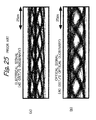
- Fig. 25(a) shows waveform of duobinary signal (electrical signal) of 40 Gbit/s generated by a prior driver
- Fig. 25(b) shows optical intensity waveforms modulated by said signal.
- an electrical signal for driving an optical modulator has asymmetrical pattern in eye apertures between upper eye opening and lower eye opening, and further an optical intensity signal modulated by said electrical signal is degraded in waveforms because of inter-symbol interference although an eye aperture is kept.
- An inter-symbol interference degrades receive sensitivity of optical duobinary signal, and dispersion tolerance so that distance for transmission is considerably decreased.
- an optical transmitter comprising bandwidth restriction means for restricting bandwidth of input electrical binary signal, an electrical-optical conversion means for converting electrical signal which is bandwidth restricted by said bandwidth restriction means to optical signal, an amplifier for amplifying an input signal of said electrical-optical conversion means so that said input signal has enough level for operating said electrical-optical conversion means, and said bandwidth restriction means being located between an output of said amplifier and an input of said electrical-optical conversion means.
- bandwidth restriction means which is implemented for instance by a low pass filter is located between an output of an amplifier for driving a modulator and an input of an optical modulator, therefore, said amplifier has only to amplify a binary NRZ signal so that inter-symbol interference problem is avoided even when it operates in saturation region.
- a waveform shaping means such as a low pass filter is implemented by a part of said amplifier or said optical modulator, thus, not only an optical transmitter is compact, but also harmful reflection between an amplifier and a filter, and/or a filter and an optical modulator is avoided so that an optical transmitter with high performance is obtained.
- Fig. 1 is a block diagram of a first embodiment of an optical transmitter according to the present invention.
- an optical transmitter comprises an input terminal 10 which receives an electrical binary data signal, a binary signal amplifier 12 for amplifying the binary data signal, a bandwidth restriction means 14 which is implemented by a low pass filter for restricting bandwidth of an output signal of the amplifier 12, an electrical-optical conversion means 16 for converting electrical signal of an output of the filter 14 to optical form, and an optical output terminal 18 coupled with an output of the electrical-optical converter 16.
- the feature in Fig. 1 is that the bandwidth restriction means 14 is located between the binary signal amplifier 12 and the electrical-optical conversion means 16, while the bandwidth restriction means in a prior art (Fig. 21) is located at an input side of an amplifier.
- the bandwidth restriction means 14 or the filter is equivalent to the circuit consisting of a one-bit delay which delays an input signal by one bit, and an adder which provides sum of an output of the one-bit delay and an input signal.
- An electrical-optical conversion means 16 may be either a semiconductor laser in which an optical source is directly modulated, or a combination of a continuous light source and an external modulator.
- An external modulator may be any type of modulator, for instance, a field absorption type modulator using a semiconductor, or a MZ (Mach Zehnder) type modulator using electrical-optical crystal such as LiNbO 3 .
- the spectrum of optical signal is designed according to a bandwidth restriction means 14.
- a bandwidth restriction means 14 As the spectrum of optical signal depends upon an input signal waveform applied to a binary signal amplifier 12, response characteristic of a binary signal amplifier 12 and an electrical-optical converter 16, the response characteristic of a bandwidth restriction means 14 is designed considering those conditions.
- an optical signal from an optical transmitter must satisfy the Nyquist criterion of zero inter-symbol interference.
- the amplitude spectrum decreases half at frequency f 0 /2 of that of D.C. component, and reaches zero at approximate f 0 .
- the maximum frequency of the signal spectrum which satisfies the Nyquist criterion I distributes between f 0 /2 and f 0 depending upon shape of spectrum.
- the maximum frequency f 0 of the signal spectrum is allowed so that it is realized by an actual low pass filter.
- a signal amplifier 12 which is apt to provide inter-symbol interference is located at an input side of a low pass filter 14, so that an output of the low pass filter 14 drives directly an electrical-optical converter 16 to provide an excellent light signal waveform.
- Fig. 3 shows a second embodiment of an optical transmitter which uses duobinary code according to the present invention.
- the bandwidth restriction code such as duobinary code which satisfies the Nyquist criterion II is used.
- the bandwidth restriction means 14b in the current embodiment is a duobinary filter which is a low pass filter having 3 dB cutoff frequency around f 0 /4.
- Fig. 4 shows a signal spectrum of an ideal duobinary signal.
- the maximum frequency of a duobinary signal spectrum is f 0 /2, however, as it is cutoff moderately, it may be implemented by using an actual filter.
- the current embodiment has a code inverter 30 and a precoder 32 before a binary signal amplifier 12.
- a code inverter 30 inverts an input code, 0 or 1, to 1 or 0.
- a precoder 32 comprises an exclusive-OR circuit 32a and a one-bit delay 32b which delays a signal by one bit duration or a period T. Inputs of the exclusive-OR circuit 32a are an output of the inverter 30 and an output of the one-bit delay 32b, and an input of the one-bit delay 32b is an output of the exclusive-OR circuit 32a.
- a ternary signal of an output of a duobinary filter 14b has a logical signal 1 corresponding to high level and low level, and logical signal 0 corresponding to intermediate level. Therefore, a receive side may correctly demodulate a receive signal by deciding whether a receive signal is at intermediate level (logical 0) or not (logical 1).
- an output (b) of an inverter 30 is an inverted form of (1,0,1,1,1,0,1) an output of a precoder 32 shown in (c) which is in NRZ form of (1,1,0,1,0,0,1)
- an output of a duobinary filter 14b is shown in (d) which is a ternary duobinary signal having level (0,+1,0,0,0,-1,0)
- an optical output of a converter 16 is shown in (e) which has (0,1,0,0,0,1,0) with a phase corresponding to the first 1 being opposite to that of the second 1.
- a signal amplifier which may cause inter-symbol interference is located before a duobinary filter, so that a distortion generated by an amplifier is removed by a duobinary filter and an output of the duobinary filter drives directly an electrical-optical converter to provide excellent optical signal waveform.
- Fig. 5 shows a third embodiment of an optical transmitter according to the present invention.
- a modified duobinary code which satisfies the Nyquist criterion III realizes bandwidth suppression similar to a duobinary code.
- a precoder in the current embodiment is a modified precoder 30' in which a delay circuit 32b' is two bits delay circuit instead of one bit delay circuit 32b in Fig. 3.
- the bandwidth restriction means in the current embodiment is a band pass filter 14c called a modified duobinary filter.
- Fig. 6 shows a spectrum of an ideal modified duobinary signal. The maximum frequency of an ideal modified duobinary signal spectrum is the same as that of a duobinary signal spectrum.
- the modified duobinary signal further suppresses D.C.
- a modified duobinary signal is a ternary signal as is the case of a duobinary signal, it needs a precoder as shown in Fig. 5, which is different from that of Fig. 3 for a duobinary signal. Because of the presence of a specific precoder, a ternary signal provided by a modified duobinary filter has a logical 1 corresponding to high level and low level, and a logical 0 corresponding to intermediate level. Therefore, a receive side may correctly demodulate a receive signal by deciding whether a receive signal is at an intermediate level or not.
- a signal shaped by a modified duobinary filter keeps waveform itself until it is transmitted into a transmission line through conversion into an optical signal, therefore, a signal amplifier which may cause inter-symbol interference is located before a modified duobinary filter.
- an electrical-optical converter is directly driven by an output of a modified duobinary filter so that an excellent optical waveform is obtained.
- Fig. 7 shows a fourth embodiment of an optical transmitter according to the present invention.
- Fig. 7 is similar to the embodiment of Fig. 3, and an electrical-optical converter is implemented by a Mach Zehnder modulator 16.
- An input signal applied to the Mach Zehnder modulator 16 is in differential form, so that a differential distributor 34 is provided to divide an output of the precoder 32 to two branches.
- the numeral 36 is an optical source which generates coherent light which is supplied to the Mach Zehnder modulator 16.
- Fig. 7 is an implementation of an optical transmitter which modulates a ternary duobinary signal into intensity and phase of light, and the logical operation of Fig. 7 is the same as that of Fig. 21.
- duobinary filters (14b-1, 14b-2) are located between amplifiers (12-1, 12-2) and a MZ light modulator 16. Because of that feature, the current embodiment provides optical signal which is free from inter-symbol interference as compared with that of a prior optical duobinary transmitter in Fig. 21.
- Fig. 8 shows measured waveforms of an electrical modulation signal of 40 Gbit/s, and a modulated optical signal of 40 Gbit/s.
- Fig. 8(a) shows waveform of electrical signal which is applied to a Mach Zehnder modulator, and has clear eye aperture on line Q-Q' having levels 1, 0 and -1.
- Fig. 8(b) is waveform of modulated optical signal having high level corresponding to electrical levels +1 and -1, and low level corresponding to electrical level 0.
- the waveforms according to the present invention have less inter-symbol interference and have large eye aperture (on line Q-Q'), as compared with those of a prior art.
- Fig. 9 shows a dispersion tolerance of 40 Gbit/s optical duobinary signal measured by using the optical transmitter in Fig. 7.
- the dispersion tolerance which satisfies power penalty less than 1 dB is 380 ps/nm, which almost coincides with the expected value by calculation. Therefore, an optical transmitter of the current embodiment realizes essentially an ideal optical duobinary signal.
- the dispersion tolerance of a prior optical transmitter for 40 Gbit/s optical duobinary signal is 200 ps/nm as shown in Fig. 24.
- the present optical transmitter is clearly better than a prior optical transmitter in view of dispersion tolerance.
- Fig. 10 shows a block diagram of a fifth embodiment of an optical transmitter according to the present invention.
- the feature of the current embodiment is that a binary signal amplifier 12 and a bandwidth restriction means 14 are integrated into a module 40 so that a connector between a binary signal amplifier 12 and a bandwidth restriction means 14 is removed.
- the current embodiment has the advantages that a number of components mounted in a transmitter is decreased, and that the effect of reflection between a binary signal amplifier 12 and a bandwidth restriction means 14 is avoided so that a signal free from inter-symbol interference is generated.
- Fig. 11 shows a block diagram of a sixth embodiment of an optical transmitter according to the present invention.
- the feature of the current embodiment is that a bandwidth restriction means 14 and an electrical-optical converter 16 are integrated into a module 42 so that a connector between a bandwidth restriction means 14 and an electrical-optical converter 16 is removed.
- the current embodiment has the advantages that a number of components mounted in a transmitter is decreased as is the case of the fifth embodiment, and that the effect of reflection between a bandwidth restriction means 14 and an electrical-optical converter 16 is avoided so that a signal free from inter-symbol interference is obtained. Further, when a binary signal amplifier 12 is mounted in the same module 42, an optical transmitter which is further compact and stable is obtained.
- Fig. 12 shows a seventh embodiment of an optical transmitter according to the present invention.
- the feature of the current embodiment is that the bandwidth restriction means and the electrical-optical converter in the sixth embodiment is implemented by a MZ light modulator 50 which uses a Z-cut Lithium-Niobate (LiNbO 3 ).
- a MZ light modulator using Lithium-Niobate takes shortened electrodes, travelling wave type electrodes, and/or specific shape of electrodes.
- the length and/or shape of electrodes are not designed for high speed operation, but designed to satisfy desired bandwidth restriction performance by using loss in an electrode, and phase mismatching between an electrical modulation signal and an optical wave which is subject to be modulated, so that a MZ light modulator doubles as a bandwidth restriction means.
- the loss in a travelling wave type electrode at f 0 /2 is always larger than the loss at frequency higher than f 0 /2, and modulation efficiency of said Mach Zehnder light intensity modulator at f 0 /2 is larger than that at frequency higher than f 0 /2, where f 0 is clock frequency of an electrical binary signal.
- modulation efficiency determined by the phase mismatching of a Mach Zehnder light intensity modulator at f 0 /2 is always larger than that at frequency higher than f 0 /2, where f 0 is clock frequency of an electrical binary signal.
- a numeral 10 is an input terminal of an electrical data signal
- 12 is an electrical amplifier
- 50 is an electrical-optical converter implemented by a Mach Zehnder light modulator.
- the numeral 36 is an optical source which generates an optical signal subject to be modulated by the modulator 50
- 18 is modulated optical signal.
- the numeral 52 is a D.C. bias terminal which accepts bias potential applied to the electrode 50a of the Mach Zehnder modulator 50
- 54 is an inductor
- 56 is a terminal resistor
- 58 is a capacitor.
- the other electrode 50b of the modulator 50 is grounded.
- An optical beam generated by the optical source 36 is separated into two beams travelling the waveguides p and q, respectively, in the modulator 50 and then two beams are combined into a single beam so that the beam is amplitude modulated by phase difference between two beams in respective waveguides.
- Fig. 13 shows the decrease of modulation efficiency caused by phase mismatching between the phase of electrical signal travelling an electrode, and the phase of optical signal travelling a waveguide. It is understood that the modulation efficiency decrease coefficient
- ⁇ m angular frequency of electrical signal (rad/s)
- ⁇ d interaction time (s) of an optical signal and an electrical signal
- c/n phase velocity (m/s) of an optical wave in an electrical-optical crystal
- c m phase velocity (m/s) of an electrical signal
- phase mismatching coefficient ⁇ is proportional to angular frequency ⁇ m of electrical modulation wave
- the modulation efficiency decreases depending upon the increase of the angular frequency of electrical modulation wave.
- the phase mismatching coefficient ⁇ is a function of interaction time ⁇ d of electrical modulation wave and optical wave to be modulated, and phase velocity c m of electrical modulation wave, therefore, the modulation frequency characteristic of the modulation efficiency decrease coefficient r is designed according to ⁇ d and c m .
- a MZ light modulator can double as a filter by designing modulation efficiency decrease coefficient r properly.
- Fig. 14 shows an eighth embodiment of an optical transmitter according to the present invention.
- the feature of the present embodiment is an optical duobinary transmitter which has a dual electrode type MZ light modulator 60 having LiNbO 3 , and each of said electrodes (61-1, 61-2) is used as a duobinary filter.
- a precoded binary NRZ signal in differential form is applied to a pair of electrodes (61-1, 61-2) of the MZ light modulator 60, so that the polarity of a signal applied to a first electrode 61-1 is opposite to the polarity of a signal applied to a second electrode 61-2.
- the electrodes function as a duobinary filter
- the electrodes are designed so that the duobinary filter has 3 dB cut-off frequency around the frequency of 1/4 of a signal clock frequency.
- the phase change in the modulated optical signal has waveforms of a ternary duobinary signal, and the MZ light modulator provides an optical duobinary signal in which the light intensity is the maximum for the maximum phase change and the minimum phase change, the light intensity is the minimum around the midpoint of the optical phase changes, and the phase of the optical signal of the maximum intensity for the maximum phase is opposite to that for the minimum phase.
- Fig. 15 shows a ninth embodiment of an optical transmitter according to the present invention.
- the feature of the current embodiment is that the travelling direction of electric modulation wave propagating on an electrode is opposite to the travelling direction of optical wave propagating in an optical waveguide in Lithium-Niobate crystal so that phase mismatching condition is generated to provide bandwidth restriction characteristic in electrodes.
- Other portions in Fig. 15 are the same as those in Fig. 14.
- optical wave generated by a light source 36 propagates in the figure from left to right, while electric wave of an output of amplifiers 12-1, and 12-2 propagate in the figure from right to left.
- the opposite travelling direction means that a sign of light velocity c/n in a waveguide and a sign of an electric modulation wave velocity c m are opposite to each other in the definition of the phase mismatching coefficient ⁇ in Fig. 13, therefore, the value (1-(c/n)c m ) is larger than 1, and the phase mismatching coefficient ⁇ is large.
- An eye aperture opens along a line R-R'. It is understood visually in Fig. 16 that the bandwidth is restricted by the phase mismatching between electrical modulation wave and light wave which is subject to be modulated, and a binary NRZ signal is converted into a ternary duobinary signal.
- a phase inverted optical duobinary signal is obtained by modifying only bias voltage of a MZ modulator in Fig. 16, and Fig. 17 shows the intensity waveforms of said phase inverted optical duobinary signal. It is understood in Fig. 17 that an eye aperture is kept as a binary signal.
- the drive voltage of the MZ modulator in Fig. 17 is half of the drive voltage requested for ordinary optical duobinary modulation, since Fig.
- Fig. 18 shows a tenth embodiment of an optical transmitter according to the present invention.
- an X-cut Lithium-Niobate MZ optical modulator is used, but not Z-cut.
- Lithium-Niobate is uni-axis crystal, having the highest modulation efficiency when electric field is applied in Z-axis direction, therefore, Z-cut crystal is usually used in an ordinary electric-optical modulator.
- Fig. 19 shows cross section (along A-A' in Fig. 15) of Z-cut Lithium-Niobate optical modulator 70.
- the numeral 71 is a substrate of Z-cut Lithium-Niobate, on which, through a silica buffer layer 72, ground electrodes 73-1, 73-2, 73-3, and a pair of signal electrodes 74-1 and 74-2 are deposited. Under the signal electrodes 74-1 and 74-1, a pair of waveguides 75-1 and 75-2 with titanium (Ti) diffused are provided.
- electric field E is applied perpendicular to a substrate surface in an optical waveguide as shown by an arrow 76, and a pair of electrodes 74-1, 74-2 must be driven complementary so that no chirp is provided, such as an optical duobinary modulation.
- Fig. 20 shows cross section (along B-B' in Fig. 18) of an X-cut Lithium-Niobate optical modulator 80 used in the embodiment of Fig. 18.
- the numeral 81 is a substrate of X-cut Lithium-Niobate, on which, through a silica buffer layer 82, ground electrodes 83-1 and 83-2, and a signal electrode 84 are deposited. In regions between signal electrodes and a ground electrode waveguide 85-1 and 85-2 with titanium diffused are provided.
- an electric field E is applied parallel to a substrate surface in an optical waveguide, as shown by an arrow 86.
- a signal electrode 84 is located at the center of two waveguides of a MZ modulator, and a pair of ground electrodes 83-1 and 83-2 are located on both ends of the substrate symmetrically to the signal electrode 84 (see Fig. 18), opposite electric fields are always applied to each of the waveguides. Therefore, a chirp is zero in principle when a single electrode MZ modulator is used.
- the current embodiment makes those electrodes having the bandwidth restriction performance, thus, an optical duobinary signal is generated with a simple structure of a MZ modulator.
- waveform shaping means such as a low pass filter is located between an electrical amplifier which drives an optical modulator, and an optical modulator, so that the electrical amplifier has only to amplify an electrical binary NRZ signal.
- a severe inter-symbol interference problem caused by the operation of the electrical amplifier in gain saturation region is avoided.
- a waveform shaping means such as a low pass filter is integrated with a driver amplifier or an optical modulator
- an optical transmitter may be compact and further harmful reflection is decreased between an amplifier and a filter, or between a filter and an optical modulator. Therefore, a bandwidth restricted optical signal close to ideal condition is generated. This is beneficial to make distance long, capacity large and cost low in an optical communication system.
Landscapes
- Physics & Mathematics (AREA)
- Electromagnetism (AREA)
- Engineering & Computer Science (AREA)
- Computer Networks & Wireless Communication (AREA)
- Signal Processing (AREA)
- Optics & Photonics (AREA)
- Optical Communication System (AREA)
- Optical Modulation, Optical Deflection, Nonlinear Optics, Optical Demodulation, Optical Logic Elements (AREA)
- Dc Digital Transmission (AREA)
Applications Claiming Priority (2)
| Application Number | Priority Date | Filing Date | Title |
|---|---|---|---|
| JP2000261114A JP3721062B2 (ja) | 2000-08-30 | 2000-08-30 | 光送信機 |
| EP01410109A EP1185006B1 (fr) | 2000-08-30 | 2001-08-29 | Emetteur optique avec limitation de la largeur de bande |
Related Parent Applications (2)
| Application Number | Title | Priority Date | Filing Date |
|---|---|---|---|
| EP01410109.1 Division | 2001-08-29 | ||
| EP01410109A Division EP1185006B1 (fr) | 2000-08-30 | 2001-08-29 | Emetteur optique avec limitation de la largeur de bande |
Publications (3)
| Publication Number | Publication Date |
|---|---|
| EP1802005A2 true EP1802005A2 (fr) | 2007-06-27 |
| EP1802005A3 EP1802005A3 (fr) | 2007-10-10 |
| EP1802005B1 EP1802005B1 (fr) | 2012-07-11 |
Family
ID=18749014
Family Applications (2)
| Application Number | Title | Priority Date | Filing Date |
|---|---|---|---|
| EP07105784A Expired - Lifetime EP1802005B1 (fr) | 2000-08-30 | 2001-08-29 | Système de transmission optique |
| EP01410109A Expired - Lifetime EP1185006B1 (fr) | 2000-08-30 | 2001-08-29 | Emetteur optique avec limitation de la largeur de bande |
Family Applications After (1)
| Application Number | Title | Priority Date | Filing Date |
|---|---|---|---|
| EP01410109A Expired - Lifetime EP1185006B1 (fr) | 2000-08-30 | 2001-08-29 | Emetteur optique avec limitation de la largeur de bande |
Country Status (3)
| Country | Link |
|---|---|
| US (2) | US7536112B2 (fr) |
| EP (2) | EP1802005B1 (fr) |
| JP (1) | JP3721062B2 (fr) |
Families Citing this family (32)
| Publication number | Priority date | Publication date | Assignee | Title |
|---|---|---|---|---|
| JP3721062B2 (ja) * | 2000-08-30 | 2005-11-30 | 日本電信電話株式会社 | 光送信機 |
| ATE260002T1 (de) * | 2002-03-04 | 2004-03-15 | Cit Alcatel | Optischer sender, system und verfahren zur übertragung von signalen mit hohen datenraten |
| GB2386779A (en) * | 2002-03-19 | 2003-09-24 | Denselight Semiconductors Pte | Multi-channel optical transmitter module |
| EP1349311A1 (fr) * | 2002-03-21 | 2003-10-01 | Alcatel | Compresseur temporel de paquets optiques à boucle de délais pour transmissions à haut-débits |
| KR100469725B1 (ko) * | 2002-09-30 | 2005-02-02 | 삼성전자주식회사 | 듀오바이너리 광 송신장치 |
| KR100469726B1 (ko) * | 2002-10-11 | 2005-02-02 | 삼성전자주식회사 | 이중 바이너리 방식의 광송신 장치 |
| KR100493095B1 (ko) * | 2002-10-16 | 2005-06-02 | 삼성전자주식회사 | 광 전송 시스템 |
| KR100480283B1 (ko) | 2002-11-19 | 2005-04-07 | 삼성전자주식회사 | 듀오바이너리 광 전송장치 |
| KR100469709B1 (ko) | 2002-11-22 | 2005-02-02 | 삼성전자주식회사 | 듀오바이너리 광 전송장치 |
| KR100566195B1 (ko) | 2003-08-27 | 2006-03-29 | 삼성전자주식회사 | 반도체 광 증폭기를 이용한 듀오바이너리 광 전송장치 |
| KR100557111B1 (ko) * | 2003-09-16 | 2006-03-03 | 삼성전자주식회사 | 듀오바이너리 광 전송장치 |
| EP1528697A1 (fr) * | 2003-10-30 | 2005-05-04 | Alcatel | Emetteur optique utilisant la modulation RZ-DPSK |
| US7508882B2 (en) * | 2003-12-04 | 2009-03-24 | Alcatel-Lucent Usa Inc. | Electrical backplane transmission using duobinary signaling |
| WO2005091534A1 (fr) * | 2004-03-24 | 2005-09-29 | Terasea Ltd. | Systeme de transmission duobinaire optique, et procede associe |
| DE602004003488T2 (de) * | 2004-07-13 | 2007-03-29 | Alcatel | Bandbegrenztes FSK Modulationsverfahren |
| KR100703267B1 (ko) | 2004-11-19 | 2007-04-03 | 삼성전자주식회사 | 색분산 내성이 강화된 이진 데이터 전기신호를 사용하는듀오바이너리 광송신기 |
| GB2428149B (en) * | 2005-07-07 | 2009-10-28 | Agilent Technologies Inc | Multimode optical fibre communication system |
| JP2007259286A (ja) * | 2006-03-24 | 2007-10-04 | Fujitsu Ltd | 光送信装置および光伝送システム |
| US7796842B2 (en) * | 2006-10-07 | 2010-09-14 | Lightwire, Inc. | AC-coupled differential drive circuit for opto-electronic modulators |
| WO2008152642A1 (fr) | 2007-06-13 | 2008-12-18 | Ramot At Tel Aviv University Ltd. | Modulateur numérique à analogique optique linéarisé |
| JP4884338B2 (ja) * | 2007-09-03 | 2012-02-29 | 日本電信電話株式会社 | 光変調器ドライバ調整装置及び調整方法 |
| JP2010028751A (ja) * | 2008-07-24 | 2010-02-04 | Toshiba Corp | コンプリメンタリー光配線装置 |
| JP2010136244A (ja) * | 2008-12-08 | 2010-06-17 | Toshiba Corp | 送信回路およびコンプリメンタリー光配線システム |
| WO2010134986A2 (fr) * | 2009-05-20 | 2010-11-25 | Neophotonics Corporation | Emetteurs-récepteurs/transpondeurs optiques à 40, 50 et 100 go/s dans des modules 300 pin et cfp msa |
| US20110052196A1 (en) * | 2009-08-27 | 2011-03-03 | Gnauck Alan H | Narrow-band DPSK apparatus, system, method |
| US20110206383A1 (en) * | 2010-02-25 | 2011-08-25 | Georgia Tech Research Corporation | Systems and methods for providing an optical information transmission system |
| DE102010048488B4 (de) * | 2010-10-14 | 2013-01-10 | Northrop Grumman Litef Gmbh | Digitaler Modulator |
| US20130177316A1 (en) * | 2012-01-06 | 2013-07-11 | Emcore Corporation | Optical communication system, and transmitter and receiver apparatus therefor |
| EP2843854B1 (fr) * | 2013-08-27 | 2018-04-04 | ADVA Optical Networking SE | Procédé, dispositif émetteur et récepteur pour transmettre un signal d'émission numérique binaire sur une liaison de transmission optique |
| US9450678B2 (en) * | 2013-10-14 | 2016-09-20 | Tyco Electronics Subsea Communications Llc | System and method using spectral shaping and expanded channel spacing |
| JP6597052B2 (ja) * | 2015-08-21 | 2019-10-30 | 住友大阪セメント株式会社 | 光変調器 |
| TWI578722B (zh) * | 2015-11-23 | 2017-04-11 | 財團法人資訊工業策進會 | Optical communication system and optical communication transmission device |
Citations (1)
| Publication number | Priority date | Publication date | Assignee | Title |
|---|---|---|---|---|
| EP1004920A2 (fr) | 1998-11-25 | 2000-05-31 | Fujitsu Limited | Modulateur optique et sa méthode de commande |
Family Cites Families (16)
| Publication number | Priority date | Publication date | Assignee | Title |
|---|---|---|---|---|
| US5271074A (en) * | 1991-11-18 | 1993-12-14 | Raytheon Company | Integrated optical waveguide apparatus |
| US5644664A (en) * | 1994-06-10 | 1997-07-01 | The United States Of America As Represented By The Secretary Of The Navy | Fiber optic digital transmission system |
| US5543952A (en) * | 1994-09-12 | 1996-08-06 | Nippon Telegraph And Telephone Corporation | Optical transmission system |
| JP3306573B2 (ja) | 1994-09-12 | 2002-07-24 | 日本電信電話株式会社 | 光送信装置および光伝送システム |
| JP3027944B2 (ja) * | 1996-08-16 | 2000-04-04 | 日本電気株式会社 | 光デュオバイナリ信号光の生成方法および光送信装置 |
| US5917638A (en) * | 1997-02-13 | 1999-06-29 | Lucent Technologies, Inc. | Duo-binary signal encoding |
| FR2781322B1 (fr) * | 1998-07-20 | 2000-09-08 | Alsthom Cge Alcatel | Dispositif d'emission de donnees optiques |
| DE69940873D1 (de) | 1998-07-29 | 2009-06-25 | Nippon Telegraph & Telephone | Optisches Übertragungssystem |
| US6415003B1 (en) * | 1998-09-11 | 2002-07-02 | National Semiconductor Corporation | Digital baseline wander correction circuit |
| JP4008617B2 (ja) * | 1999-03-30 | 2007-11-14 | 沖電気工業株式会社 | 光源の周波数安定化装置 |
| US6483953B1 (en) * | 1999-05-11 | 2002-11-19 | Jds Uniphase Corporation | External optical modulation using non-co-linear compensation networks |
| JP3910003B2 (ja) * | 2000-05-29 | 2007-04-25 | 富士通株式会社 | 光受信局、光通信システム及び分散制御方法 |
| US6728277B1 (en) * | 2000-08-28 | 2004-04-27 | Emcore Corporation | Envelope biasing for laser transmitters |
| JP3721062B2 (ja) * | 2000-08-30 | 2005-11-30 | 日本電信電話株式会社 | 光送信機 |
| KR100492971B1 (ko) * | 2002-10-31 | 2005-06-07 | 삼성전자주식회사 | 듀오바이너리 광 전송장치 |
| KR100520648B1 (ko) * | 2003-05-16 | 2005-10-13 | 삼성전자주식회사 | 반도체 광 증폭기를 이용한 듀오바이너리 광 전송장치 |
-
2000
- 2000-08-30 JP JP2000261114A patent/JP3721062B2/ja not_active Expired - Lifetime
-
2001
- 2001-08-28 US US09/939,716 patent/US7536112B2/en not_active Expired - Lifetime
- 2001-08-29 EP EP07105784A patent/EP1802005B1/fr not_active Expired - Lifetime
- 2001-08-29 EP EP01410109A patent/EP1185006B1/fr not_active Expired - Lifetime
-
2008
- 2008-04-21 US US12/081,733 patent/US7542631B2/en not_active Expired - Lifetime
Patent Citations (1)
| Publication number | Priority date | Publication date | Assignee | Title |
|---|---|---|---|---|
| EP1004920A2 (fr) | 1998-11-25 | 2000-05-31 | Fujitsu Limited | Modulateur optique et sa méthode de commande |
Non-Patent Citations (1)
| Title |
|---|
| ED L. WOOTEN ET AL., IEEE JOURNAL OF SELECTED TOPICS IN QUANTUM ELECTRONICS, vol. 6, no. 1, 2000, pages 69 - 82 |
Also Published As
| Publication number | Publication date |
|---|---|
| JP3721062B2 (ja) | 2005-11-30 |
| EP1185006A2 (fr) | 2002-03-06 |
| EP1802005A3 (fr) | 2007-10-10 |
| US20080205903A1 (en) | 2008-08-28 |
| EP1185006A3 (fr) | 2006-01-18 |
| EP1185006B1 (fr) | 2013-03-06 |
| US7542631B2 (en) | 2009-06-02 |
| US7536112B2 (en) | 2009-05-19 |
| EP1802005B1 (fr) | 2012-07-11 |
| US20020033984A1 (en) | 2002-03-21 |
| JP2002077059A (ja) | 2002-03-15 |
Similar Documents
| Publication | Publication Date | Title |
|---|---|---|
| EP1185006B1 (fr) | Emetteur optique avec limitation de la largeur de bande | |
| EP1612972B1 (fr) | Procédé et dispositif de génération de signaux CRZ-DPSK optiques | |
| US20030112487A1 (en) | Method and apparatus for transmitting a modulated optical signal | |
| EP0841587A2 (fr) | Modulateur optique du type Mach-Zehnder à modulation de fréquence parasite (chirp) contrôlable | |
| JP2000081597A (ja) | 光デ―タ送信装置 | |
| GB2329089A (en) | Optical transmission system with cross-phase modulation compensation | |
| JP3292826B2 (ja) | 光データ送信デバイス | |
| US7155071B2 (en) | Device for Mach-Zehnder modulator bias control for duobinary optical transmission and associated system and method | |
| US20030147656A1 (en) | Optical transmitter and optical fiber transmission system having the same | |
| US6606424B2 (en) | Apparatus and method for optical modulation and demodulation | |
| JP2000022640A (ja) | 光送信器及び光伝送システム | |
| EP1404036B1 (fr) | Dispositif de transmission optique duobinaire | |
| EP1617576B1 (fr) | Format de modulation FSK à largeur de bande limitée | |
| KR100492971B1 (ko) | 듀오바이너리 광 전송장치 | |
| JP2004312678A (ja) | デュオバイナリ光伝送装置 | |
| US20040240888A1 (en) | System and method for alternate mark inversion and duobinary optical transmission | |
| EP1411656A2 (fr) | Système de transmission optique duobinaire RZ avec suppression de porteuse | |
| US20020167703A1 (en) | Tandem filters for reducing intersymbol interference in optical communications systems | |
| Cartledge | Comparison of effective/spl alpha/-parameters for semiconductor Mach-Zehnder optical modulators | |
| EP1202476B1 (fr) | Système et émetteur pour la transmission de données optiques | |
| US7412173B2 (en) | Apparatus for generating optical carrier suppressed return-to-zero | |
| Mauro et al. | Advanced modulation formats for fiber optic communication systems | |
| JPH09275375A (ja) | 光通信装置 | |
| EP1528697A1 (fr) | Emetteur optique utilisant la modulation RZ-DPSK | |
| Paloi | Long-haul signal transmission using various modulator formats and frequency conversion |
Legal Events
| Date | Code | Title | Description |
|---|---|---|---|
| PUAI | Public reference made under article 153(3) epc to a published international application that has entered the european phase |
Free format text: ORIGINAL CODE: 0009012 |
|
| 17P | Request for examination filed |
Effective date: 20070405 |
|
| AC | Divisional application: reference to earlier application |
Ref document number: 1185006 Country of ref document: EP Kind code of ref document: P |
|
| AK | Designated contracting states |
Kind code of ref document: A2 Designated state(s): AT BE BG CH CY CZ DE DK EE ES FI FR GB GR HU IE IS IT LI LT LU LV MC MT NL PL PT RO SE SI SK TR |
|
| AX | Request for extension of the european patent |
Extension state: AL BA HR MK YU |
|
| PUAL | Search report despatched |
Free format text: ORIGINAL CODE: 0009013 |
|
| AK | Designated contracting states |
Kind code of ref document: A3 Designated state(s): AT BE BG CH CY CZ DE DK EE ES FI FR GB GR HU IE IS IT LI LT LU LV MC MT NL PL PT RO SE SI SK TR |
|
| AX | Request for extension of the european patent |
Extension state: AL BA HR MK YU |
|
| AKX | Designation fees paid |
Designated state(s): DE FR GB |
|
| 17Q | First examination report despatched |
Effective date: 20110818 |
|
| GRAP | Despatch of communication of intention to grant a patent |
Free format text: ORIGINAL CODE: EPIDOSNIGR1 |
|
| GRAS | Grant fee paid |
Free format text: ORIGINAL CODE: EPIDOSNIGR3 |
|
| GRAA | (expected) grant |
Free format text: ORIGINAL CODE: 0009210 |
|
| AC | Divisional application: reference to earlier application |
Ref document number: 1185006 Country of ref document: EP Kind code of ref document: P |
|
| AK | Designated contracting states |
Kind code of ref document: B1 Designated state(s): DE FR GB |
|
| REG | Reference to a national code |
Ref country code: GB Ref legal event code: FG4D |
|
| REG | Reference to a national code |
Ref country code: DE Ref legal event code: R096 Ref document number: 60146823 Country of ref document: DE Effective date: 20120906 |
|
| PLBE | No opposition filed within time limit |
Free format text: ORIGINAL CODE: 0009261 |
|
| STAA | Information on the status of an ep patent application or granted ep patent |
Free format text: STATUS: NO OPPOSITION FILED WITHIN TIME LIMIT |
|
| 26N | No opposition filed |
Effective date: 20130412 |
|
| REG | Reference to a national code |
Ref country code: DE Ref legal event code: R097 Ref document number: 60146823 Country of ref document: DE Effective date: 20130412 |
|
| REG | Reference to a national code |
Ref country code: FR Ref legal event code: PLFP Year of fee payment: 16 |
|
| REG | Reference to a national code |
Ref country code: FR Ref legal event code: PLFP Year of fee payment: 17 |
|
| REG | Reference to a national code |
Ref country code: FR Ref legal event code: PLFP Year of fee payment: 18 |
|
| REG | Reference to a national code |
Ref country code: DE Ref legal event code: R082 Ref document number: 60146823 Country of ref document: DE Representative=s name: KEIL & SCHAAFHAUSEN PATENTANWAELTE PARTGMBB, DE Ref country code: DE Ref legal event code: R082 Ref document number: 60146823 Country of ref document: DE Representative=s name: KEIL & SCHAAFHAUSEN PATENT- UND RECHTSANWAELTE, DE |
|
| PGFP | Annual fee paid to national office [announced via postgrant information from national office to epo] |
Ref country code: GB Payment date: 20200826 Year of fee payment: 20 Ref country code: FR Payment date: 20200821 Year of fee payment: 20 Ref country code: DE Payment date: 20200819 Year of fee payment: 20 |
|
| REG | Reference to a national code |
Ref country code: DE Ref legal event code: R071 Ref document number: 60146823 Country of ref document: DE |
|
| REG | Reference to a national code |
Ref country code: GB Ref legal event code: PE20 Expiry date: 20210828 |
|
| PG25 | Lapsed in a contracting state [announced via postgrant information from national office to epo] |
Ref country code: GB Free format text: LAPSE BECAUSE OF EXPIRATION OF PROTECTION Effective date: 20210828 |