EP1801883A1 - Photo sensor and organic light-emitting display using the same - Google Patents
Photo sensor and organic light-emitting display using the same Download PDFInfo
- Publication number
- EP1801883A1 EP1801883A1 EP06256521A EP06256521A EP1801883A1 EP 1801883 A1 EP1801883 A1 EP 1801883A1 EP 06256521 A EP06256521 A EP 06256521A EP 06256521 A EP06256521 A EP 06256521A EP 1801883 A1 EP1801883 A1 EP 1801883A1
- Authority
- EP
- European Patent Office
- Prior art keywords
- organic light
- photo
- photo sensor
- layer
- diode
- Prior art date
- Legal status (The legal status is an assumption and is not a legal conclusion. Google has not performed a legal analysis and makes no representation as to the accuracy of the status listed.)
- Ceased
Links
Images


Classifications
-
- H—ELECTRICITY
- H10—SEMICONDUCTOR DEVICES; ELECTRIC SOLID-STATE DEVICES NOT OTHERWISE PROVIDED FOR
- H10F—INORGANIC SEMICONDUCTOR DEVICES SENSITIVE TO INFRARED RADIATION, LIGHT, ELECTROMAGNETIC RADIATION OF SHORTER WAVELENGTH OR CORPUSCULAR RADIATION
- H10F39/00—Integrated devices, or assemblies of multiple devices, comprising at least one element covered by group H10F30/00, e.g. radiation detectors comprising photodiode arrays
- H10F39/10—Integrated devices
-
- H—ELECTRICITY
- H10—SEMICONDUCTOR DEVICES; ELECTRIC SOLID-STATE DEVICES NOT OTHERWISE PROVIDED FOR
- H10F—INORGANIC SEMICONDUCTOR DEVICES SENSITIVE TO INFRARED RADIATION, LIGHT, ELECTROMAGNETIC RADIATION OF SHORTER WAVELENGTH OR CORPUSCULAR RADIATION
- H10F55/00—Radiation-sensitive semiconductor devices covered by groups H10F10/00, H10F19/00 or H10F30/00 being structurally associated with electric light sources and electrically or optically coupled thereto
- H10F55/10—Radiation-sensitive semiconductor devices covered by groups H10F10/00, H10F19/00 or H10F30/00 being structurally associated with electric light sources and electrically or optically coupled thereto wherein the radiation-sensitive semiconductor devices control the electric light source, e.g. image converters, image amplifiers or image storage devices
- H10F55/17—Radiation-sensitive semiconductor devices covered by groups H10F10/00, H10F19/00 or H10F30/00 being structurally associated with electric light sources and electrically or optically coupled thereto wherein the radiation-sensitive semiconductor devices control the electric light source, e.g. image converters, image amplifiers or image storage devices wherein the radiation-sensitive semiconductor devices have potential barriers
-
- H—ELECTRICITY
- H10—SEMICONDUCTOR DEVICES; ELECTRIC SOLID-STATE DEVICES NOT OTHERWISE PROVIDED FOR
- H10F—INORGANIC SEMICONDUCTOR DEVICES SENSITIVE TO INFRARED RADIATION, LIGHT, ELECTROMAGNETIC RADIATION OF SHORTER WAVELENGTH OR CORPUSCULAR RADIATION
- H10F71/00—Manufacture or treatment of devices covered by this subclass
- H10F71/131—Recrystallisation; Crystallization of amorphous or microcrystalline semiconductors
-
- H—ELECTRICITY
- H10—SEMICONDUCTOR DEVICES; ELECTRIC SOLID-STATE DEVICES NOT OTHERWISE PROVIDED FOR
- H10K—ORGANIC ELECTRIC SOLID-STATE DEVICES
- H10K59/00—Integrated devices, or assemblies of multiple devices, comprising at least one organic light-emitting element covered by group H10K50/00
- H10K59/10—OLED displays
- H10K59/12—Active-matrix OLED [AMOLED] displays
- H10K59/13—Active-matrix OLED [AMOLED] displays comprising photosensors that control luminance
-
- H—ELECTRICITY
- H10—SEMICONDUCTOR DEVICES; ELECTRIC SOLID-STATE DEVICES NOT OTHERWISE PROVIDED FOR
- H10F—INORGANIC SEMICONDUCTOR DEVICES SENSITIVE TO INFRARED RADIATION, LIGHT, ELECTROMAGNETIC RADIATION OF SHORTER WAVELENGTH OR CORPUSCULAR RADIATION
- H10F55/00—Radiation-sensitive semiconductor devices covered by groups H10F10/00, H10F19/00 or H10F30/00 being structurally associated with electric light sources and electrically or optically coupled thereto
- H10F55/10—Radiation-sensitive semiconductor devices covered by groups H10F10/00, H10F19/00 or H10F30/00 being structurally associated with electric light sources and electrically or optically coupled thereto wherein the radiation-sensitive semiconductor devices control the electric light source, e.g. image converters, image amplifiers or image storage devices
- H10F55/15—Radiation-sensitive semiconductor devices covered by groups H10F10/00, H10F19/00 or H10F30/00 being structurally associated with electric light sources and electrically or optically coupled thereto wherein the radiation-sensitive semiconductor devices control the electric light source, e.g. image converters, image amplifiers or image storage devices wherein the radiation-sensitive devices and the electric light source are all semiconductor devices
- H10F55/155—Radiation-sensitive semiconductor devices covered by groups H10F10/00, H10F19/00 or H10F30/00 being structurally associated with electric light sources and electrically or optically coupled thereto wherein the radiation-sensitive semiconductor devices control the electric light source, e.g. image converters, image amplifiers or image storage devices wherein the radiation-sensitive devices and the electric light source are all semiconductor devices formed in, or on, a common substrate
-
- Y—GENERAL TAGGING OF NEW TECHNOLOGICAL DEVELOPMENTS; GENERAL TAGGING OF CROSS-SECTIONAL TECHNOLOGIES SPANNING OVER SEVERAL SECTIONS OF THE IPC; TECHNICAL SUBJECTS COVERED BY FORMER USPC CROSS-REFERENCE ART COLLECTIONS [XRACs] AND DIGESTS
- Y02—TECHNOLOGIES OR APPLICATIONS FOR MITIGATION OR ADAPTATION AGAINST CLIMATE CHANGE
- Y02E—REDUCTION OF GREENHOUSE GAS [GHG] EMISSIONS, RELATED TO ENERGY GENERATION, TRANSMISSION OR DISTRIBUTION
- Y02E10/00—Energy generation through renewable energy sources
- Y02E10/50—Photovoltaic [PV] energy
-
- Y—GENERAL TAGGING OF NEW TECHNOLOGICAL DEVELOPMENTS; GENERAL TAGGING OF CROSS-SECTIONAL TECHNOLOGIES SPANNING OVER SEVERAL SECTIONS OF THE IPC; TECHNICAL SUBJECTS COVERED BY FORMER USPC CROSS-REFERENCE ART COLLECTIONS [XRACs] AND DIGESTS
- Y02—TECHNOLOGIES OR APPLICATIONS FOR MITIGATION OR ADAPTATION AGAINST CLIMATE CHANGE
- Y02P—CLIMATE CHANGE MITIGATION TECHNOLOGIES IN THE PRODUCTION OR PROCESSING OF GOODS
- Y02P70/00—Climate change mitigation technologies in the production process for final industrial or consumer products
- Y02P70/50—Manufacturing or production processes characterised by the final manufactured product
Definitions
- the present invention relates to organic light-emitting displays.
- the present invention relates to an organic light-emitting display having a photo sensor capable of providing improved luminance control thereof.
- an organic light-emitting display is a flat display device where voltage may be applied to a plurality of layers interposed between two electrodes, i.e., an anode and a cathode, to combine electrons and holes to form images.
- the conventional organic light-emitting display may include a hole injection layer, a hole transport layer, at least one organic light-emitting layer, an electron injection layer, and an electron transport layer. Accordingly, holes may be injected into the hole injection layer from the anode electrode and transported into the organic light-emitting layer through the hole transport layer. Similarly, electrons from the cathode may be injected into the electron injection layer and transported to the organic light-emitting layer through the electron transport layer. The transported holes and electrons may be combined with one another in the organic light-emitting layer to form excitons, and thereby, emit visible light.
- Such a conventional organic light emitting layer of the organic light-emitting display may deteriorate over time and, thereby, reduce display luminance.
- the brightness of light emitted from the organic light emitting layer may deviate from the required brightness value, thereby reducing the image quality of the organic light emitting display and its overall lifespan.
- Attempts have been made to improve the brightness of the organic light-emitting display device by incorporating a photo diode therein, such that a constant electric signal from the photo diode may trigger constant luminance from the organic light-emitting display, regardless of the deterioration state of the organic light-emitting layer.
- a conventional photo diode may have a limited electric signal output, thereby limiting the luminance control efficiency, i.e., reducing the luminance adjustment range.
- an organic light-emitting display according to Claim 8.
- Preferred features of this aspect are set out in Claims 9 and 10.
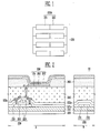
- FIG. 1 illustrates a plan view of a photo sensor according to an embodiment of the present invention
- FIG. 2 illustrates a cross-sectional view of an organic light-emitting display having the photo sensor illustrated in FIG. 1;
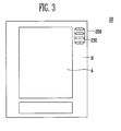
- FIG. 3 illustrates a plan view of an organic light-emitting display having the photo sensor illustrated in FIG. 1;
- FIG. 4 illustrates a plan view of a photo sensor according to another embodiment of the present invention.
- FIG. 5 illustrates a cross-sectional view of an organic light-emitting display having the photo sensor illustrated in FIG. 4;
- FIG. 6 illustrates a plan view of an organic light-emitting display having the photo sensor illustrated in FIG. 4;
- FIG. 7 illustrates a perspective view of an exemplary portable electronic device having an organic light-emitting display device according to an embodiment of the present invention.
- a photo sensor 230 may include a plurality of photo diodes 230A, i.e., at least two photo diodes 230A.
- Each photo diode 230A may have a first region 231 and a second region 232, such that the first and second regions 231 and 232 may be adjacent to one another.
- each photo diode 230A may be formed of amorphous silicon and crystallized by a predetermined thermal treatment, i.e., any appropriate heat treatment of amorphous silicon material as determined by a person skilled in the art, to form a polycrystalline silicon.
- a high concentration of N-type impurity ions may be implanted in the polycrystalline silicon of the first region 231 to form an N-type doping region 231, and a high concentration of P-type impurity ions may be implanted in the polycrystalline silicon of the second region 232 to form a P-type doping region 232.
- each photo diode 230A may be a PN-type photo diode, i.e., an N-type doping region 231 and a P-type doping region, while the N-type and P-type doping regions 231 and 232 may be positioned on a same plane, adjacent to one another.
- a current amount flowing through a photo diode may be proportional to an area of a photo diode when a current density is constant.
- I d J ⁇ A
- I d an electric current
- J is a current density
- A is an area of the photo diode.
- the plurality of photo diodes 230A of the photo sensor 230 may be connected to one another in parallel, such that a total area of the photo sensor 230 and the current therethrough may be increased, while the current value through each individual photo diode 230A may remain constant.
- Such a structure of photo diodes may facilitate current control through the photo sensor 230 and, thereby, enhance the control of electric signals, i.e., range of output current or voltage, generated by the photo sensor 230.
- a junction therebetween may become fully depleted, such that charges may be produced in response to light incident through a surface of the depletion region.
- the plurality of photo diodes 230A may output an electrical signal with respect to the produced charges and proportionately to the density of the light.
- an organic light-emitting display 20 includes a substrate 200, a thin film transistor 220, an organic light-emitting diode 250, and a photo sensor 230.
- the substrate 200 may be made of any insulating material, e.g., glass, plastic, silicon, synthetic resin, and so forth, as determined by one of ordinary skill in the art.
- the substrate 200 may be transparent, e.g., a glass substrate.
- the substrate 200 may be formed to have a pixel region A and a non-pixel region B therein, as illustrated in FIGS. 2-3, such that the pixel region A includes a central region of the substrate 200 that is capable of displaying images, e.g., an area including the organic light emitting diode 250, and the non-pixel region B includes a peripheral region of the substrate 200 surrounding the pixel region A that is not capable of displaying images, i.e., regions other than the pixel region A.
- the thin film transistor 220 of the organic light-emitting display 20 is formed in the pixel region A of the substrate 200 by crystallizing an amorphous silicon layer into a low temperature polysilicon (LTPS) via, for example, laser irradiation.
- the thin film transistor 220 includes a semiconductor layer 221, a gate electrode 222 with a predetermined pattern, and source/drain electrodes 223, wherein a gate insulating layer 221 a is disposed between the semiconductor layer 221 and the gate electrode 222 on the semiconductor layer 221 and an inter-dielectric layer 222a is disposed between the gate electrode 222 and the source/drain electrode 223.
- the gate insulating layer 221a is deposited on the substrate 200 and over the semiconductor layer 221 and the photo diode 220, as illustrated in FIG. 2, such that a portion of the gate insulating layer 221a is positioned on the substrate 200 between the semiconductor layer 221 of the thin film transistor 220 and the photo sensor 230 to separate therebetween.
- the source/drain electrodes 223 are disposed over the inter-dielectric layer 222a and are electrically connected with both sides of the semiconductor layer 221 via a contact hole 123a formed through the gate insulating layer 221a and the inter-dielectric layer 222a.
- the organic light-emitting diode 250 of the light-emitting display device 20 is formed on the substrate 200 and include a first electrode layer 251, a second electrode layer 253, and a light emitting layer 252 therebetween.
- the organic light-emitting diode 250 is electrically connected to the thin film transistor 220, i.e., any one of the source and drain electrodes 223, via a hole.
- the first electrode layer 251 of the organic light-emitting diode 250 may be made of any suitable transparent conductor, e.g., indium-tin-oxide (ITO), indium-zinc-oxide (IZO), zinc oxide (ZnO), and so forth.
- the second electrode layer 253 of the organic light-emitting diode 250 may be formed on the first electrode layer 251.
- the light emitting layer 252 of the organic light-emitting diode 250 is formed between the first and second electrode layers 251 and 253, respectively.
- the light emitting layer 252 may be formed to partially expose the first electrode layer 251.
- the light emitting layer 252 may include a hole injecting layer, a hole transport layer, an electron transport layer and an electron injecting layer. Accordingly, the light emitting layer 252 may generate light when holes and electron injected from the first and second electrode layers 251 and 253, respectively, are coupled therein.
- the photo sensor 230 of the light-emitting display device 20 may be any suitable optical sensor capable of receiving a light signal and converting the light signal into an electrical signal, e.g., current or voltage.
- the photo sensor may be a semiconductor device having an optical detecting function, e.g., a plurality of photo diodes with a light detecting function at a junction thereof.
- an optical detecting function e.g., a plurality of photo diodes with a light detecting function at a junction thereof.
- a conductivity of a plurality of photo diodes may be modulated with respect to a light signal detected therein
- a plurality of photo diodes functioning as a photo sensor may convert light signals into electrical signals with respect to changes of current flow therein as related to optical changes.
- the photo sensor 230 may be identical to the photo sensor 230 previously described with respect to FIG. 1, and therefore, its detailed structure and operation with respect to the N-type doping region 231 and P-type doping region 232 will not be repeated herein.
- the photo sensor 230 may include a plurality of photo diodes 230A formed of amorphous silicon in the non-pixel region B of the substrate 200, as illustrated in FIGS. 2-3, and crystallized as polycrystalline silicon through a predetermined heat treatment, i.e., any appropriate heat treatment of amorphous silicon material as determined by a person skilled in the art.
- the plurality of photo diodes 230A may be connected to one another in parallel, as illustrated in FIG. 3, thereby providing a constant current value through each photo diode 230A, while having increased photo sensor 230 area and current flow.
- a plurality of photo diodes 230A connected in parallel to one another and having a total area of W ⁇ L may include n individual photo diodes 230A, while each individual photo diode 230A may have an area of W/n ⁇ L.
- the photo sensor 230 absorbs light emitted from the organic light-emitting diode 250 and converts it into electrical signals.
- light absorbed by the photo sensor 230 i.e., actual luminance values of the organic light-emitting diode 250
- a predetermined luminance reference value Any deviation of the actual luminance values from the predetermined luminance reference value may be controlled by the photo sensor 230 via electrical signals, thereby facilitating constant luminance output from the organic light-emitting diode 250, i.e., light generated by the light emitting layer 252.
- electric signals generated by the photo sensor 230 may be inputted into a comparator for comparing actual luminance values with the predetermined luminance reference value. More specifically, when the electric signal outputted from the photo sensor 230, i.e., signals representing actual luminance values, is lower than the predetermined luminance reference value, the comparator may generate a control signal to increase the luminance of light emitted by the light-emitting layer 252 of the organic light-emitting diode 250. Similarly, when the electric signal outputted from the photo sensor 230 is higher than the predetermined luminance reference value, the comparator may generate a control signal to reduce the luminance of light emitted by the light-emitting layer 252 of the organic light-emitting diode 250.
- electric signals i.e., electric current or a voltage
- the photo sensor 230 may maintain constant luminance of light generated in the light-emitting layer 252 of the organic light-emitting diode 250.
- a light-emitting display device 20 may also include a planarization layer 240.
- the planarization layer 240 may be formed on the thin film transistor 220 by depositing a layer of an oxide, e.g., silicon oxide (SiO 2 ) or a nitride, e.g., silicon nitride (SiNx).
- the planarization layer 240 may be positioned between the thin film transistor 220 and the organic light emitting diode 250, and a portion of the planarization layer 240 may be etched to expose one of the source and drain electrodes 223 in order to provide a connection between the thin film transistor 220 and the first electrode 251 of the organic light-emitting diode 250.
- the light-emitting display device 20 may also include a pixel defining layer 260.
- the pixel defining film 260 may be formed on the planarization layer 240, such that the pixel defining film 260 may include an opening portion (not shown) to at least partially expose the first electrode layer 251 of the organic light emitting diode 250.
- the pixel defining layer 250 may be positioned between the first and second electrode layers 251 and 253 of the organic light emitting diode 250.
- the pixel defining film 260 may be made of an organic insulation material, e.g., acrylic organic compounds, polyamides, polyimides, and so forth.
- the light-emitting display device 20 may also include a buffer layer 210 on the substrate 200.
- the buffer layer 210 may be formed of a single layer of silicon oxide (SiO 2 ) or silicon nitride (SiN x ), or the buffer layer 210 may have a multi-layer structure.
- the buffer layer 210 may minimize diffusion of impurities into the thin film transistor 220 and the photo diode 230 during post-processing thereof.
- a photo sensor 330 includes a plurality of photo diodes 330A connected to one another in parallel and having a first region 331, a second region 333, and an intrinsic region 332, such that the first region 331, the second region 333, and the intrinsic region 332 are formed on one plane and positioned adjacent to one another, i.e., PIN-type photo diode.
- the intrinsic region 332 is positioned between the first and second regions 331 and 333.
- the photo sensor 330 is formed in a similar manner to the photo sensor 230 described previously with respect to FIG. 1, and therefore, the detailed description of forming N-type and P-type impurity regions therein, i.e., doping regions corresponding to the first and second regions 331 and 333, will not be repeated.
- the intrinsic region 332 of each photo diode 330A of the photo sensor 330 may be formed of polycrystalline silicon between the N-type doping region 331 and the P-type doping region 333, such that no impurities may be injected therein. Accordingly, when an anode voltage is applied to the P-type doping region 333 and a cathode voltage is applied to the N-type doping region 331 of each photo diode 330A, each respective intrinsic region 332 may become fully depleted and, thereby, absorb internal or external light. The intrinsic region 332 generates charges with respect to the absorbed light through its surface, and, subsequently, convert the charges into electric signals.
- the intrinsic region 332 increases the thickness of a depletion layer of each photo diode 3330A, thereby decreasing a capacitance thereof.
- Such a decrease in capacitance of each photo diode 330A increases the operation speed and decreases the power consumption thereof, as compared to a conventional photo sensor.
- the photo sensor 330 has a lower dark current, i.e., a current flow when a photo sensor is not exposed to light, as compared to the conventional photo sensor.
- an organic light-emitting display 30 includes a substrate 300 having a pixel region C and a non-pixel region D, a thin film transistor 320 on the pixel region C of the substrate 300, an organic light-emitting diode 350 electrically connected to the thin film transistor 320, and a photo sensor 330 having a plurality of photo diodes 330A at the non-pixel region D of the substrate 300. At least two of the photo diodes 330A are connected to one another in parallel, as illustrated in FIG. 6.
- the organic light-emitting display 300 further includes a buffer layer 310 deposited on the substrate 300, a planarization layer 340 deposited between the organic light emitting diode 350 and the thin film transistor 320, and a pixel defining film 360.
- the structures of the substrate 300, the thin film transistor 320, the organic light-emitting diode 350, the buffer layer 310, the planarization layer 340, and the pixel defining film 360 are similar to the respective structures of the substrate 200, the thin film transistor 220, the organic light-emitting diode 250, the buffer layer 210, the planarization layer 240, and the pixel defining film 260 described previously with respect to FIGS. 2-3 and, therefore, their detailed description will not be repeated hereinafter.
- the structure of the photo sensor 330 are identical to the structure of the photo sensor 330 previously described with respect to FIG. 4, and therefore, its detailed structure and operation will not be repeated herein.
- the organic light-emitting display device may be employed in any portable apparatus, e.g., a portable phone, a digital camera, a television, a view finder type and a monitor direct view type video tape recorder, a car navigation device, a pager, an electronic note, an electronic calculator, a word processor, a workstation, a videophone, a POS terminal, and any device having a touch panel.
- a portable phone e.g., a portable phone, a digital camera, a television, a view finder type and a monitor direct view type video tape recorder, a car navigation device, a pager, an electronic note, an electronic calculator, a word processor, a workstation, a videophone, a POS terminal, and any device having a touch panel.
- a portable phone 400 may include an organic light-emitting display panel 410 with the photo sensor (not shown) described previously with respect to FIGS. 1 and 4, a plurality of operation buttons 420, a receiving hole 430, and a transmitting hole 440.
- the embodiment of the portable phone 400 according to the present invention illustrated in FIG. 7 is advantageous because the photo sensor employed in the display panel 410 minimizes the necessity of installing a special opening portion for a mounting space. Further, the photo sensor in the portable phone 400 can detect an accurate amount of internal/external light absorbed therein, such that a displayed image may have an enhanced luminance control in terms of its surrounding ambient light.
- a structure of a photo sensor having a plurality of photo diodes connected to one another in parallel may be advantageous in improving luminance control of organic light emitting layers.
- current values through the photo sensor, i.e., plurality of photo diodes may be increased to compensate for deteriorated material of an organic light-emitting layer and provide constant luminance.
- an integration rate of the photo sensor is improved to increase the availability of the total design.
Landscapes
- Engineering & Computer Science (AREA)
- Microelectronics & Electronic Packaging (AREA)
- Electroluminescent Light Sources (AREA)
- Thin Film Transistor (AREA)
- Light Receiving Elements (AREA)
Abstract
Description
- The present invention relates to organic light-emitting displays. In particular, the present invention relates to an organic light-emitting display having a photo sensor capable of providing improved luminance control thereof.
- In general, an organic light-emitting display is a flat display device where voltage may be applied to a plurality of layers interposed between two electrodes, i.e., an anode and a cathode, to combine electrons and holes to form images. More particularly, the conventional organic light-emitting display may include a hole injection layer, a hole transport layer, at least one organic light-emitting layer, an electron injection layer, and an electron transport layer. Accordingly, holes may be injected into the hole injection layer from the anode electrode and transported into the organic light-emitting layer through the hole transport layer. Similarly, electrons from the cathode may be injected into the electron injection layer and transported to the organic light-emitting layer through the electron transport layer. The transported holes and electrons may be combined with one another in the organic light-emitting layer to form excitons, and thereby, emit visible light.
- Such a conventional organic light emitting layer of the organic light-emitting display may deteriorate over time and, thereby, reduce display luminance. In other words, once the organic light-emitting layer deteriorates, the brightness of light emitted from the organic light emitting layer may deviate from the required brightness value, thereby reducing the image quality of the organic light emitting display and its overall lifespan. Attempts have been made to improve the brightness of the organic light-emitting display device by incorporating a photo diode therein, such that a constant electric signal from the photo diode may trigger constant luminance from the organic light-emitting display, regardless of the deterioration state of the organic light-emitting layer. However, a conventional photo diode may have a limited electric signal output, thereby limiting the luminance control efficiency, i.e., reducing the luminance adjustment range.
- Accordingly, there exists a need for an organic light-emitting display device with a photo diode capable of controlling luminance thereof by efficient electric signals.
- According to a first aspect of the invention there is provided a photosensot according to Claim 1. Preferred features of this aspect are set out in Claims 2-7.
- According to a second aspect of the invention there is provided an organic light-emitting display according to Claim 8. Preferred features of this aspect are set out in Claims 9 and 10.
- According to a third aspect of the invention there is provided a portable electronic apparatus according to Claim 11.
- The above and other features and advantages of the present invention will become more apparent to those of ordinary skill in the art by describing in detail exemplary embodiments thereof with reference to the attached drawings, in which:
- FIG. 1 illustrates a plan view of a photo sensor according to an embodiment of the present invention;
- FIG. 2 illustrates a cross-sectional view of an organic light-emitting display having the photo sensor illustrated in FIG. 1;
- FIG. 3 illustrates a plan view of an organic light-emitting display having the photo sensor illustrated in FIG. 1;
- FIG. 4 illustrates a plan view of a photo sensor according to another embodiment of the present invention;
- FIG. 5 illustrates a cross-sectional view of an organic light-emitting display having the photo sensor illustrated in FIG. 4;
- FIG. 6 illustrates a plan view of an organic light-emitting display having the photo sensor illustrated in FIG. 4;
- FIG. 7 illustrates a perspective view of an exemplary portable electronic device having an organic light-emitting display device according to an embodiment of the present invention.
- The present invention will now be described more fully hereinafter with reference to the accompanying drawings, in which exemplary embodiments of the invention are illustrated. The invention may, however, be embodied in different forms and should not be construed as limited to the embodiments set forth herein. Rather, these embodiments are provided so that this disclosure will be thorough and complete, and will fully convey the scope of the invention to those skilled in the art.
- In the figures, the dimensions of layers and regions may be exaggerated for clarity of illustration. It will also be understood that when a layer or an element is referred to as being "on" another layer, element or substrate, it can be directly on the other layer, element or substrate, or intervening layers or elements may also be present. Further, it will be understood that when a layer or an element is referred to as being "under" another layer or element, it can be directly under, or one or more intervening layers or elements may also be present. In addition, it will also be understood that when a layer or an element is referred to as being "between" two layers or elements, it can be the only layer or element between the two layers or elements, or one or more intervening layers or elements may also be present. Like reference numerals refer to like elements throughout.
- Hereinafter, an embodiment of a photo sensor according to the present invention will be described in more detail below with reference to FIG. 1. As illustrated in FIG. 1, a
photo sensor 230 according to an embodiment of the present invention may include a plurality ofphoto diodes 230A, i.e., at least twophoto diodes 230A. Eachphoto diode 230A may have afirst region 231 and asecond region 232, such that the first andsecond regions - In particular, each
photo diode 230A may be formed of amorphous silicon and crystallized by a predetermined thermal treatment, i.e., any appropriate heat treatment of amorphous silicon material as determined by a person skilled in the art, to form a polycrystalline silicon. Next, a high concentration of N-type impurity ions may be implanted in the polycrystalline silicon of thefirst region 231 to form an N-type doping region 231, and a high concentration of P-type impurity ions may be implanted in the polycrystalline silicon of thesecond region 232 to form a P-type doping region 232. Accordingly, eachphoto diode 230A may be a PN-type photo diode, i.e., an N-type doping region 231 and a P-type doping region, while the N-type and P-type doping regions - In general, a current amount flowing through a photo diode may be proportional to an area of a photo diode when a current density is constant. In other words, and with respect to equation (1) below, the greater an area of a photo diode, the higher a current amount through it.

where Id is an electric current, J is a current density, and A is an area of the photo diode. However, formation of a photo diode in an organic light emitting display may restrict the area thereof. - Accordingly, the plurality of
photo diodes 230A of thephoto sensor 230 may be connected to one another in parallel, such that a total area of thephoto sensor 230 and the current therethrough may be increased, while the current value through eachindividual photo diode 230A may remain constant. Such a structure of photo diodes may facilitate current control through thephoto sensor 230 and, thereby, enhance the control of electric signals, i.e., range of output current or voltage, generated by thephoto sensor 230. In particular, when an anode voltage is applied to the P-type doping region 232 of thephoto diodes 230A, and a cathode voltage is applied to the N-type doping region 231 of thephoto diodes 230A, a junction therebetween may become fully depleted, such that charges may be produced in response to light incident through a surface of the depletion region. The plurality ofphoto diodes 230A may output an electrical signal with respect to the produced charges and proportionately to the density of the light. - An embodiment of the
photo sensor 230 in an organic light-emitting display will be described in more detail with respect to FIGS. 2-3. As illustrated in FIGS. 2-3, an organic light-emittingdisplay 20 includes asubstrate 200, athin film transistor 220, an organic light-emitting diode 250, and aphoto sensor 230. - The
substrate 200 may be made of any insulating material, e.g., glass, plastic, silicon, synthetic resin, and so forth, as determined by one of ordinary skill in the art. Preferably thesubstrate 200 may be transparent, e.g., a glass substrate. Additionally, thesubstrate 200 may be formed to have a pixel region A and a non-pixel region B therein, as illustrated in FIGS. 2-3, such that the pixel region A includes a central region of thesubstrate 200 that is capable of displaying images, e.g., an area including the organiclight emitting diode 250, and the non-pixel region B includes a peripheral region of thesubstrate 200 surrounding the pixel region A that is not capable of displaying images, i.e., regions other than the pixel region A. - The
thin film transistor 220 of the organic light-emittingdisplay 20 is formed in the pixel region A of thesubstrate 200 by crystallizing an amorphous silicon layer into a low temperature polysilicon (LTPS) via, for example, laser irradiation. Thethin film transistor 220 includes asemiconductor layer 221, agate electrode 222 with a predetermined pattern, and source/drain electrodes 223, wherein agate insulating layer 221 a is disposed between thesemiconductor layer 221 and thegate electrode 222 on thesemiconductor layer 221 and aninter-dielectric layer 222a is disposed between thegate electrode 222 and the source/drain electrode 223. Thegate insulating layer 221a is deposited on thesubstrate 200 and over thesemiconductor layer 221 and thephoto diode 220, as illustrated in FIG. 2, such that a portion of thegate insulating layer 221a is positioned on thesubstrate 200 between thesemiconductor layer 221 of thethin film transistor 220 and thephoto sensor 230 to separate therebetween. The source/drain electrodes 223 are disposed over theinter-dielectric layer 222a and are electrically connected with both sides of thesemiconductor layer 221 via acontact hole 123a formed through thegate insulating layer 221a and theinter-dielectric layer 222a. - The organic light-
emitting diode 250 of the light-emittingdisplay device 20 is formed on thesubstrate 200 and include afirst electrode layer 251, asecond electrode layer 253, and alight emitting layer 252 therebetween. The organic light-emittingdiode 250 is electrically connected to thethin film transistor 220, i.e., any one of the source and drainelectrodes 223, via a hole. - The
first electrode layer 251 of the organic light-emittingdiode 250 may be made of any suitable transparent conductor, e.g., indium-tin-oxide (ITO), indium-zinc-oxide (IZO), zinc oxide (ZnO), and so forth. Thesecond electrode layer 253 of the organic light-emittingdiode 250 may be formed on thefirst electrode layer 251. Thelight emitting layer 252 of the organic light-emittingdiode 250 is formed between the first and second electrode layers 251 and 253, respectively. In particular, thelight emitting layer 252 may be formed to partially expose thefirst electrode layer 251. Further, thelight emitting layer 252 may include a hole injecting layer, a hole transport layer, an electron transport layer and an electron injecting layer. Accordingly, thelight emitting layer 252 may generate light when holes and electron injected from the first and second electrode layers 251 and 253, respectively, are coupled therein. - The
photo sensor 230 of the light-emittingdisplay device 20 may be any suitable optical sensor capable of receiving a light signal and converting the light signal into an electrical signal, e.g., current or voltage. For example, the photo sensor may be a semiconductor device having an optical detecting function, e.g., a plurality of photo diodes with a light detecting function at a junction thereof. In other words, because electrons or holes may be generated by means of absorption of photons, and, therefore, a conductivity of a plurality of photo diodes may be modulated with respect to a light signal detected therein, a plurality of photo diodes functioning as a photo sensor may convert light signals into electrical signals with respect to changes of current flow therein as related to optical changes. - Accordingly, the
photo sensor 230 may be identical to thephoto sensor 230 previously described with respect to FIG. 1, and therefore, its detailed structure and operation with respect to the N-type doping region 231 and P-type doping region 232 will not be repeated herein. Thephoto sensor 230 may include a plurality ofphoto diodes 230A formed of amorphous silicon in the non-pixel region B of thesubstrate 200, as illustrated in FIGS. 2-3, and crystallized as polycrystalline silicon through a predetermined heat treatment, i.e., any appropriate heat treatment of amorphous silicon material as determined by a person skilled in the art. - In particular, formation of the plurality of
photo diodes 230A may be restricted in the non-pixel region B in terms of space. Therefore, according to an exemplary embodiment of the present invention, the plurality ofphoto diodes 230A may be connected to one another in parallel, as illustrated in FIG. 3, thereby providing a constant current value through eachphoto diode 230A, while having increasedphoto sensor 230 area and current flow. For example, a plurality ofphoto diodes 230A connected in parallel to one another and having a total area of W×L may include nindividual photo diodes 230A, while eachindividual photo diode 230A may have an area of W/n×L. - The
photo sensor 230 absorbs light emitted from the organic light-emittingdiode 250 and converts it into electrical signals. In particular, light absorbed by thephoto sensor 230, i.e., actual luminance values of the organic light-emittingdiode 250, is compared to a predetermined luminance reference value. Any deviation of the actual luminance values from the predetermined luminance reference value may be controlled by thephoto sensor 230 via electrical signals, thereby facilitating constant luminance output from the organic light-emittingdiode 250, i.e., light generated by thelight emitting layer 252. - For example, electric signals generated by the
photo sensor 230 may be inputted into a comparator for comparing actual luminance values with the predetermined luminance reference value. More specifically, when the electric signal outputted from thephoto sensor 230, i.e., signals representing actual luminance values, is lower than the predetermined luminance reference value, the comparator may generate a control signal to increase the luminance of light emitted by the light-emittinglayer 252 of the organic light-emittingdiode 250. Similarly, when the electric signal outputted from thephoto sensor 230 is higher than the predetermined luminance reference value, the comparator may generate a control signal to reduce the luminance of light emitted by the light-emittinglayer 252 of the organic light-emittingdiode 250. Alternatively, electric signals, i.e., electric current or a voltage, generated by thephoto sensor 230 with respect to an amount of light absorbed from the organic light-emittingdiode 250 may be supplied to a controller, so that the controller may output a respective control signal for controlling the luminance of the light-emittinglayer 252 with respect to the light emitted therefrom. Accordingly, thephoto sensor 230 may maintain constant luminance of light generated in the light-emittinglayer 252 of the organic light-emittingdiode 250. - A light-emitting
display device 20 according to an embodiment of the present invention may also include aplanarization layer 240. Theplanarization layer 240 may be formed on thethin film transistor 220 by depositing a layer of an oxide, e.g., silicon oxide (SiO2) or a nitride, e.g., silicon nitride (SiNx). In particular, theplanarization layer 240 may be positioned between thethin film transistor 220 and the organiclight emitting diode 250, and a portion of theplanarization layer 240 may be etched to expose one of the source and drainelectrodes 223 in order to provide a connection between thethin film transistor 220 and thefirst electrode 251 of the organic light-emittingdiode 250. - The light-emitting
display device 20 according to an embodiment of the present invention may also include apixel defining layer 260. Thepixel defining film 260 may be formed on theplanarization layer 240, such that thepixel defining film 260 may include an opening portion (not shown) to at least partially expose thefirst electrode layer 251 of the organiclight emitting diode 250. In particular, thepixel defining layer 250 may be positioned between the first and second electrode layers 251 and 253 of the organiclight emitting diode 250. Thepixel defining film 260 may be made of an organic insulation material, e.g., acrylic organic compounds, polyamides, polyimides, and so forth. - The light-emitting
display device 20 according to an embodiment of the present invention may also include abuffer layer 210 on thesubstrate 200. Thebuffer layer 210 may be formed of a single layer of silicon oxide (SiO2) or silicon nitride (SiNx), or thebuffer layer 210 may have a multi-layer structure. Thebuffer layer 210 may minimize diffusion of impurities into thethin film transistor 220 and thephoto diode 230 during post-processing thereof. - In another embodiment of the present invention, illustrated in FIG. 4, a
photo sensor 330 includes a plurality of photo diodes 330A connected to one another in parallel and having afirst region 331, asecond region 333, and anintrinsic region 332, such that thefirst region 331, thesecond region 333, and theintrinsic region 332 are formed on one plane and positioned adjacent to one another, i.e., PIN-type photo diode. In particular, theintrinsic region 332 is positioned between the first andsecond regions photo sensor 330 is formed in a similar manner to thephoto sensor 230 described previously with respect to FIG. 1, and therefore, the detailed description of forming N-type and P-type impurity regions therein, i.e., doping regions corresponding to the first andsecond regions - The
intrinsic region 332 of each photo diode 330A of thephoto sensor 330 may be formed of polycrystalline silicon between the N-type doping region 331 and the P-type doping region 333, such that no impurities may be injected therein. Accordingly, when an anode voltage is applied to the P-type doping region 333 and a cathode voltage is applied to the N-type doping region 331 of each photo diode 330A, each respectiveintrinsic region 332 may become fully depleted and, thereby, absorb internal or external light. Theintrinsic region 332 generates charges with respect to the absorbed light through its surface, and, subsequently, convert the charges into electric signals. Without intending to be bound by theory, it is believed that theintrinsic region 332 increases the thickness of a depletion layer of each photo diode 3330A, thereby decreasing a capacitance thereof. Such a decrease in capacitance of each photo diode 330A increases the operation speed and decreases the power consumption thereof, as compared to a conventional photo sensor. Additionally, thephoto sensor 330 has a lower dark current, i.e., a current flow when a photo sensor is not exposed to light, as compared to the conventional photo sensor. - Another embodiment of the
photo sensor 330 in an organic light-emitting display will be described in more detail with respect to FIGS. 5-6. As illustrated in FIGS. 5-6, an organic light-emittingdisplay 30 includes asubstrate 300 having a pixel region C and a non-pixel region D, athin film transistor 320 on the pixel region C of thesubstrate 300, an organic light-emittingdiode 350 electrically connected to thethin film transistor 320, and aphoto sensor 330 having a plurality of photo diodes 330A at the non-pixel region D of thesubstrate 300. At least two of the photo diodes 330A are connected to one another in parallel, as illustrated in FIG. 6. - The organic light-emitting
display 300 further includes abuffer layer 310 deposited on thesubstrate 300, aplanarization layer 340 deposited between the organiclight emitting diode 350 and thethin film transistor 320, and apixel defining film 360. - The structures of the
substrate 300, thethin film transistor 320, the organic light-emittingdiode 350, thebuffer layer 310, theplanarization layer 340, and thepixel defining film 360 are similar to the respective structures of thesubstrate 200, thethin film transistor 220, the organic light-emittingdiode 250, thebuffer layer 210, theplanarization layer 240, and thepixel defining film 260 described previously with respect to FIGS. 2-3 and, therefore, their detailed description will not be repeated hereinafter. Similarly, the structure of thephoto sensor 330 are identical to the structure of thephoto sensor 330 previously described with respect to FIG. 4, and therefore, its detailed structure and operation will not be repeated herein. - The organic light-emitting display device according to the embodiments previously described with respect to FIGS. 1-6 may be employed in any portable apparatus, e.g., a portable phone, a digital camera, a television, a view finder type and a monitor direct view type video tape recorder, a car navigation device, a pager, an electronic note, an electronic calculator, a word processor, a workstation, a videophone, a POS terminal, and any device having a touch panel.
- In particular, as illustrated in FIG. 7, a
portable phone 400 may include an organic light-emittingdisplay panel 410 with the photo sensor (not shown) described previously with respect to FIGS. 1 and 4, a plurality ofoperation buttons 420, a receivinghole 430, and a transmittinghole 440. - The embodiment of the
portable phone 400 according to the present invention illustrated in FIG. 7 is advantageous because the photo sensor employed in thedisplay panel 410 minimizes the necessity of installing a special opening portion for a mounting space. Further, the photo sensor in theportable phone 400 can detect an accurate amount of internal/external light absorbed therein, such that a displayed image may have an enhanced luminance control in terms of its surrounding ambient light. - In accordance with the present invention, a structure of a photo sensor having a plurality of photo diodes connected to one another in parallel may be advantageous in improving luminance control of organic light emitting layers. In particular, current values through the photo sensor, i.e., plurality of photo diodes, may be increased to compensate for deteriorated material of an organic light-emitting layer and provide constant luminance. Moreover, an integration rate of the photo sensor is improved to increase the availability of the total design.
- Embodiments of the present invention have been disclosed herein, and although specific terms are employed, they are used and are to be interpreted in a generic and descriptive sense only and not for purpose of limitation. Accordingly, it will be understood by those of ordinary skill in the art that various changes in form and details may be made without departing from the scope of the present invention as set forth in the following claims.
Claims (11)
- A photo sensor comprising a plurality of photo diodes connected to one another in parallel.
- A photo sensor according to claim 1, wherein each photo diode is a PIN photo diode.
- A photo sensor according to claim 2, wherein each PIN photo diode includes an intrinsic region between an N-type doping region and a P-type doping region.
- A photo sensor according to claim 1, wherein each photo diode is a PN diode.
- A photo sensor according to claim 4, wherein each PN photo diode includes an N-type doping region adjacent to a P-type doping region.
- A photo sensor according to claim 5, wherein the N-type doping region and the P-type doping region are on a same plane.
- A photo sensor according to any one of claims 1 to 5, wherein the plurality of photo diodes are capable of absorbing external light and outputting a corresponding electric signal.
- An organic light-emitting display, comprising:a substrate having a pixel region and a non-pixel region;a thin film transistor on the substrate;an organic light-emitting diode electrically connected to the thin film transistor; anda photo sensor according to any one of claims 1 to 7.
- An organic light-emitting display according to claim 8, wherein the photo sensor is positioned on the non-pixel region of the substrate.
- A organic light-emitting display according to claim 8 or 9, wherein the photo sensor is capable of receiving light from the organic light-emitting diode and generate a corresponding electric signal.
- A portable electronic apparatus, comprising an organic light-emitting display device according to any one of claims 8 to 10.
Applications Claiming Priority (2)
| Application Number | Priority Date | Filing Date | Title |
|---|---|---|---|
| KR1020050127228A KR100729047B1 (en) | 2005-12-21 | 2005-12-21 | OLED display having a photodiode |
| KR1020060109487A KR100821070B1 (en) | 2006-11-07 | 2006-11-07 | Photodiode and organic electroluminescent display using same |
Publications (1)
| Publication Number | Publication Date |
|---|---|
| EP1801883A1 true EP1801883A1 (en) | 2007-06-27 |
Family
ID=37888254
Family Applications (1)
| Application Number | Title | Priority Date | Filing Date |
|---|---|---|---|
| EP06256521A Ceased EP1801883A1 (en) | 2005-12-21 | 2006-12-21 | Photo sensor and organic light-emitting display using the same |
Country Status (3)
| Country | Link |
|---|---|
| US (1) | US8477125B2 (en) |
| EP (1) | EP1801883A1 (en) |
| JP (1) | JP2007173832A (en) |
Cited By (4)
| Publication number | Priority date | Publication date | Assignee | Title |
|---|---|---|---|---|
| EP2037502A2 (en) | 2007-09-14 | 2009-03-18 | Samsung Mobile Display Co., Ltd. | Light emitting display device and method of fabricating the same |
| CN101325181B (en) * | 2008-08-05 | 2010-06-09 | 友达光电股份有限公司 | Thin film transistor array substrate and manufacturing method thereof |
| EP2012361A3 (en) * | 2007-07-04 | 2010-08-18 | Samsung Mobile Display Co., Ltd. | Organic light emitting element and method of manufacturing the same |
| CN110366780A (en) * | 2017-01-15 | 2019-10-22 | 赛因托鲁株式会社 | photodetector array |
Families Citing this family (26)
| Publication number | Priority date | Publication date | Assignee | Title |
|---|---|---|---|---|
| KR100776498B1 (en) * | 2006-06-09 | 2007-11-16 | 삼성에스디아이 주식회사 | Organic electroluminescent display and manufacturing method thereof |
| TW200825563A (en) * | 2006-12-11 | 2008-06-16 | Innolux Display Corp | Light supply device and liquid crystal display device using the same |
| TWI355106B (en) * | 2007-05-07 | 2011-12-21 | Chunghwa Picture Tubes Ltd | Organic photodetector and fabricating method of or |
| KR100840099B1 (en) * | 2007-07-04 | 2008-06-19 | 삼성에스디아이 주식회사 | Manufacturing method of organic electroluminescent device provided with photo diamond |
| TWI344026B (en) * | 2007-07-18 | 2011-06-21 | Au Optronics Corp | A photo detector and a display panel having the same |
| CN100570878C (en) * | 2007-07-27 | 2009-12-16 | 友达光电股份有限公司 | Light sensor and display panel with the same |
| TWI353063B (en) * | 2007-07-27 | 2011-11-21 | Au Optronics Corp | Photo detector and method for fabricating the same |
| US8743077B1 (en) * | 2007-08-01 | 2014-06-03 | Sipix Imaging, Inc. | Front light system for reflective displays |
| KR100884458B1 (en) * | 2007-09-14 | 2009-02-20 | 삼성모바일디스플레이주식회사 | Organic electroluminescent device and manufacturing method thereof |
| KR100957948B1 (en) * | 2008-02-19 | 2010-05-13 | 삼성모바일디스플레이주식회사 | Optical sensor and flat panel display device using the same |
| US20100114679A1 (en) * | 2008-11-02 | 2010-05-06 | Yang Pan | Programmable advertising panel powered by solar cells and communiation means thereof |
| CN102810551B (en) * | 2012-07-03 | 2015-07-22 | 深圳市华星光电技术有限公司 | Display device and method for converting light energy to electric energy by display device |
| US9070648B2 (en) * | 2012-11-27 | 2015-06-30 | Apple Inc. | Electronic devices with display-integrated light sensors |
| US9935152B2 (en) | 2012-12-27 | 2018-04-03 | General Electric Company | X-ray detector having improved noise performance |
| CN103107172B (en) * | 2013-01-15 | 2015-10-21 | 深圳典邦科技有限公司 | The integrated back of the body of micro-display is according to the OLED image transceiver device of imageing sensor |
| US9917133B2 (en) | 2013-12-12 | 2018-03-13 | General Electric Company | Optoelectronic device with flexible substrate |
| US9257480B2 (en) | 2013-12-30 | 2016-02-09 | General Electric Company | Method of manufacturing photodiode detectors |
| EP3108286B1 (en) * | 2014-02-19 | 2024-01-10 | PA.Cotte Family Holding GmbH | Display device |
| DE102014009677A1 (en) * | 2014-02-19 | 2015-08-20 | Pierre-Alain Cotte | Display device with improved contrast |
| EP3117204B1 (en) | 2014-03-13 | 2021-06-16 | General Electric Company | Curved digital x-ray detector for weld inspection |
| ES2881685T3 (en) | 2016-03-02 | 2021-11-30 | Pa Cotte Family Holding Gmbh | Procedure for the manufacture of a display device and display device |
| WO2017214971A1 (en) * | 2016-06-17 | 2017-12-21 | Boe Technology Group Co., Ltd. | Touch display substrate, touch display apparatus having the same, pixel arrangement, and fabricating method thereof |
| CN106887212A (en) | 2017-03-28 | 2017-06-23 | 京东方科技集团股份有限公司 | A kind of OLED display and its brightness adjusting method |
| CN108073331A (en) * | 2018-02-26 | 2018-05-25 | 武汉华星光电技术有限公司 | The preparation method of array substrate, touching display screen and array substrate |
| US10796639B1 (en) * | 2019-09-27 | 2020-10-06 | Int Tech Co., Ltd. | Display device and method for calibrating the same |
| CN113964172B (en) * | 2021-11-23 | 2025-08-15 | 京东方科技集团股份有限公司 | Array substrate, manufacturing method thereof, display panel and display device |
Citations (11)
| Publication number | Priority date | Publication date | Assignee | Title |
|---|---|---|---|---|
| US20010052597A1 (en) * | 2000-06-20 | 2001-12-20 | U.S. Philips Corporation | Light-emitting matrix array display devices with light sensing elements |
| US20020180672A1 (en) * | 2000-01-11 | 2002-12-05 | Semiconductor Energy Laboratory Co., Ltd., A Japan Corporation | Semiconductor display device |
| WO2004019123A1 (en) * | 2002-08-24 | 2004-03-04 | Koninklijke Philips Electronics N.V. | Manufacture of electronic devices comprising thin-film circuit elements |
| EP1463117A2 (en) * | 2003-03-28 | 2004-09-29 | Eastman Kodak Company | Oled display with photosensor |
| WO2004109641A1 (en) * | 2003-06-11 | 2004-12-16 | Koninklijke Philips Electronics N.V. | Colour electroluminescent display devices |
| US20040263069A1 (en) * | 2003-06-27 | 2004-12-30 | Shunpei Yamazaki | Display device and electronic device |
| US20050035932A1 (en) * | 2003-06-30 | 2005-02-17 | Sanyo Electric Co., Ltd. | Electroluminescent display device and manufacturing method of the same |
| US20050093466A1 (en) * | 2003-09-30 | 2005-05-05 | Sanyo Electric Co., Ltd. | Electroluminescent display device |
| WO2005093838A1 (en) * | 2004-03-24 | 2005-10-06 | Koninklijke Philips Electronics N.V. | Electroluminescent display devices |
| US20050237317A1 (en) * | 2004-04-23 | 2005-10-27 | Eastman Kodak Company | OLED display and touch screen |
| US20050248264A1 (en) * | 2004-05-05 | 2005-11-10 | Eastman Kodak Company | OLED display with composite photosensor |
Family Cites Families (21)
| Publication number | Priority date | Publication date | Assignee | Title |
|---|---|---|---|---|
| US3812518A (en) * | 1973-01-02 | 1974-05-21 | Gen Electric | Photodiode with patterned structure |
| JPS5311358B2 (en) * | 1973-03-27 | 1978-04-20 | ||
| JPS61120466A (en) * | 1984-11-16 | 1986-06-07 | Fujitsu Ltd | Semiconductor light detecting element |
| JPH02143573A (en) * | 1988-11-25 | 1990-06-01 | Ricoh Co Ltd | Photoelectric conversion device |
| JPH039562A (en) * | 1989-06-07 | 1991-01-17 | Sharp Corp | Semiconductor device |
| JP3091882B2 (en) | 1990-11-26 | 2000-09-25 | 株式会社半導体エネルギー研究所 | Semiconductor device and manufacturing method thereof |
| JPH04296054A (en) | 1991-03-25 | 1992-10-20 | Shimadzu Corp | Photodiode |
| KR100550020B1 (en) | 1997-03-12 | 2006-10-31 | 세이코 엡슨 가부시키가이샤 | Pixel circuits, displays and electronics equipped with current-driven light emitting devices |
| US6111305A (en) * | 1997-10-09 | 2000-08-29 | Nippon Telegraph And Telephone Corporation | P-I-N semiconductor photodetector |
| JP4145495B2 (en) * | 2000-01-11 | 2008-09-03 | 株式会社半導体エネルギー研究所 | Display device, computer, video camera, digital camera, goggle type display, navigation system, sound playback device, game machine, portable information terminal, and image playback device |
| US6995753B2 (en) | 2000-06-06 | 2006-02-07 | Semiconductor Energy Laboratory Co., Ltd. | Display device and method of manufacturing the same |
| JP5110748B2 (en) | 2000-06-06 | 2012-12-26 | 株式会社半導体エネルギー研究所 | Display device |
| JP2002072963A (en) * | 2000-06-12 | 2002-03-12 | Semiconductor Energy Lab Co Ltd | Light emitting module, driving method thereof, and optical sensor |
| JP2002176162A (en) * | 2000-08-10 | 2002-06-21 | Semiconductor Energy Lab Co Ltd | Area sensor and display device provided with area sensor |
| GB2367945B (en) * | 2000-08-16 | 2004-10-20 | Secr Defence | Photodetector circuit |
| JP3942169B2 (en) * | 2002-08-29 | 2007-07-11 | 東北パイオニア株式会社 | Driving device and driving method of light emitting display panel |
| KR100961548B1 (en) | 2002-12-23 | 2010-06-07 | 매그나칩 반도체 유한회사 | Method for manufacturing a horizontal p-i-n diode |
| JP2004253646A (en) * | 2003-02-20 | 2004-09-09 | Toshiba Matsushita Display Technology Co Ltd | Method for manufacturing polycrystalline silicon film and method for manufacturing display device |
| JP2005128089A (en) * | 2003-10-21 | 2005-05-19 | Tohoku Pioneer Corp | Luminescent display device |
| GB2410826A (en) * | 2004-02-07 | 2005-08-10 | Sharp Kk | Active matrix liquid crystal display |
| JP4007336B2 (en) * | 2004-04-12 | 2007-11-14 | セイコーエプソン株式会社 | Pixel circuit driving method, pixel circuit, electro-optical device, and electronic apparatus |
-
2006
- 2006-12-20 US US11/641,842 patent/US8477125B2/en active Active
- 2006-12-21 EP EP06256521A patent/EP1801883A1/en not_active Ceased
- 2006-12-21 JP JP2006344356A patent/JP2007173832A/en active Pending
Patent Citations (11)
| Publication number | Priority date | Publication date | Assignee | Title |
|---|---|---|---|---|
| US20020180672A1 (en) * | 2000-01-11 | 2002-12-05 | Semiconductor Energy Laboratory Co., Ltd., A Japan Corporation | Semiconductor display device |
| US20010052597A1 (en) * | 2000-06-20 | 2001-12-20 | U.S. Philips Corporation | Light-emitting matrix array display devices with light sensing elements |
| WO2004019123A1 (en) * | 2002-08-24 | 2004-03-04 | Koninklijke Philips Electronics N.V. | Manufacture of electronic devices comprising thin-film circuit elements |
| EP1463117A2 (en) * | 2003-03-28 | 2004-09-29 | Eastman Kodak Company | Oled display with photosensor |
| WO2004109641A1 (en) * | 2003-06-11 | 2004-12-16 | Koninklijke Philips Electronics N.V. | Colour electroluminescent display devices |
| US20040263069A1 (en) * | 2003-06-27 | 2004-12-30 | Shunpei Yamazaki | Display device and electronic device |
| US20050035932A1 (en) * | 2003-06-30 | 2005-02-17 | Sanyo Electric Co., Ltd. | Electroluminescent display device and manufacturing method of the same |
| US20050093466A1 (en) * | 2003-09-30 | 2005-05-05 | Sanyo Electric Co., Ltd. | Electroluminescent display device |
| WO2005093838A1 (en) * | 2004-03-24 | 2005-10-06 | Koninklijke Philips Electronics N.V. | Electroluminescent display devices |
| US20050237317A1 (en) * | 2004-04-23 | 2005-10-27 | Eastman Kodak Company | OLED display and touch screen |
| US20050248264A1 (en) * | 2004-05-05 | 2005-11-10 | Eastman Kodak Company | OLED display with composite photosensor |
Cited By (8)
| Publication number | Priority date | Publication date | Assignee | Title |
|---|---|---|---|---|
| EP2012361A3 (en) * | 2007-07-04 | 2010-08-18 | Samsung Mobile Display Co., Ltd. | Organic light emitting element and method of manufacturing the same |
| US8592881B2 (en) | 2007-07-04 | 2013-11-26 | Samsung Display Co., Ltd. | Organic light emitting element and method of manufacturing the same |
| US9368558B2 (en) | 2007-07-04 | 2016-06-14 | Samsung Display Co., Ltd. | Organic light emitting element and method of manufacturing the same |
| EP2037502A2 (en) | 2007-09-14 | 2009-03-18 | Samsung Mobile Display Co., Ltd. | Light emitting display device and method of fabricating the same |
| EP2037502A3 (en) * | 2007-09-14 | 2012-10-10 | Samsung Display Co., Ltd. | Light emitting display device and method of fabricating the same |
| CN101325181B (en) * | 2008-08-05 | 2010-06-09 | 友达光电股份有限公司 | Thin film transistor array substrate and manufacturing method thereof |
| CN110366780A (en) * | 2017-01-15 | 2019-10-22 | 赛因托鲁株式会社 | photodetector array |
| CN110366780B (en) * | 2017-01-15 | 2023-04-25 | 赛因托鲁株式会社 | photodetector array |
Also Published As
| Publication number | Publication date |
|---|---|
| US20070138951A1 (en) | 2007-06-21 |
| JP2007173832A (en) | 2007-07-05 |
| US8477125B2 (en) | 2013-07-02 |
Similar Documents
| Publication | Publication Date | Title |
|---|---|---|
| US8477125B2 (en) | Photo sensor and organic light-emitting display using the same | |
| US7994517B2 (en) | Organic light-emitting display device and method for fabricating the same | |
| KR100840098B1 (en) | Organic electroluminescent device and manufacturing method thereof | |
| EP1865560B1 (en) | Organic light-emitting display device | |
| CN110349981B (en) | Light detection device of integrated infrared pixel of display screen | |
| TW201131752A (en) | Amoled display with optical feedback compensation | |
| US8022622B2 (en) | Organic light-emitting display device including a photo diode | |
| US20220005888A1 (en) | Array Substrate and Method for Manufacturing the Same, and Display Device | |
| KR100684675B1 (en) | Optical sensors and displays | |
| CN100511702C (en) | Organic light-emitting display device | |
| US20110102305A1 (en) | Light-emitting device | |
| US7915649B2 (en) | Light emitting display device and method of fabricating the same | |
| CN1996611A (en) | Organic electroluminescence display element and manufacturing method thereof | |
| CN1992296A (en) | Photo sensor and organic light-emitting display using the same | |
| US20200035746A1 (en) | Imaging panel | |
| CN101388405B (en) | Light emitting display device and method of fabricating the same | |
| CN101388402A (en) | Organic light emitting display and manufacturing method thereof | |
| KR100821070B1 (en) | Photodiode and organic electroluminescent display using same | |
| CN114551499B (en) | Display screen and electronic equipment | |
| KR100848337B1 (en) | Flat panel display | |
| KR100722111B1 (en) | OLED display having a photodiode | |
| US12310131B2 (en) | Photoelectric conversion panel | |
| KR100759689B1 (en) | Organic electroluminescent display |
Legal Events
| Date | Code | Title | Description |
|---|---|---|---|
| PUAI | Public reference made under article 153(3) epc to a published international application that has entered the european phase |
Free format text: ORIGINAL CODE: 0009012 |
|
| 17P | Request for examination filed |
Effective date: 20070109 |
|
| AK | Designated contracting states |
Kind code of ref document: A1 Designated state(s): AT BE BG CH CY CZ DE DK EE ES FI FR GB GR HU IE IS IT LI LT LU LV MC NL PL PT RO SE SI SK TR |
|
| AX | Request for extension of the european patent |
Extension state: AL BA HR MK YU |
|
| AKX | Designation fees paid |
Designated state(s): DE FR GB HU |
|
| 17Q | First examination report despatched |
Effective date: 20081219 |
|
| RAP1 | Party data changed (applicant data changed or rights of an application transferred) |
Owner name: SAMSUNG MOBILE DISPLAY CO., LTD. |
|
| RAP1 | Party data changed (applicant data changed or rights of an application transferred) |
Owner name: SAMSUNG DISPLAY CO., LTD. |
|
| STAA | Information on the status of an ep patent application or granted ep patent |
Free format text: STATUS: THE APPLICATION HAS BEEN REFUSED |
|
| 18R | Application refused |
Effective date: 20130124 |