EP1801874B1 - Packaged electronic device and semiconductor device with a back-side conductive layer - Google Patents
Packaged electronic device and semiconductor device with a back-side conductive layer Download PDFInfo
- Publication number
- EP1801874B1 EP1801874B1 EP06125848.9A EP06125848A EP1801874B1 EP 1801874 B1 EP1801874 B1 EP 1801874B1 EP 06125848 A EP06125848 A EP 06125848A EP 1801874 B1 EP1801874 B1 EP 1801874B1
- Authority
- EP
- European Patent Office
- Prior art keywords
- substrate
- conductive layer
- layer
- thickness
- high frequency
- Prior art date
- Legal status (The legal status is an assumption and is not a legal conclusion. Google has not performed a legal analysis and makes no representation as to the accuracy of the status listed.)
- Ceased
Links
Images



Classifications
-
- H—ELECTRICITY
- H10—SEMICONDUCTOR DEVICES; ELECTRIC SOLID-STATE DEVICES NOT OTHERWISE PROVIDED FOR
- H10W—GENERIC PACKAGES, INTERCONNECTIONS, CONNECTORS OR OTHER CONSTRUCTIONAL DETAILS OF DEVICES COVERED BY CLASS H10
- H10W42/00—Arrangements for protection of devices
- H10W42/20—Arrangements for protection of devices protecting against electromagnetic or particle radiation, e.g. light, X-rays, gamma-rays or electrons
-
- H—ELECTRICITY
- H10—SEMICONDUCTOR DEVICES; ELECTRIC SOLID-STATE DEVICES NOT OTHERWISE PROVIDED FOR
- H10W—GENERIC PACKAGES, INTERCONNECTIONS, CONNECTORS OR OTHER CONSTRUCTIONAL DETAILS OF DEVICES COVERED BY CLASS H10
- H10W42/00—Arrangements for protection of devices
- H10W42/20—Arrangements for protection of devices protecting against electromagnetic or particle radiation, e.g. light, X-rays, gamma-rays or electrons
- H10W42/281—Arrangements for protection of devices protecting against electromagnetic or particle radiation, e.g. light, X-rays, gamma-rays or electrons characterised by their materials
- H10W42/287—Arrangements for protection of devices protecting against electromagnetic or particle radiation, e.g. light, X-rays, gamma-rays or electrons characterised by their materials materials for magnetic shielding, e.g. ferromagnetic materials
-
- H—ELECTRICITY
- H10—SEMICONDUCTOR DEVICES; ELECTRIC SOLID-STATE DEVICES NOT OTHERWISE PROVIDED FOR
- H10W—GENERIC PACKAGES, INTERCONNECTIONS, CONNECTORS OR OTHER CONSTRUCTIONAL DETAILS OF DEVICES COVERED BY CLASS H10
- H10W44/00—Electrical arrangements for controlling or matching impedance
- H10W44/20—Electrical arrangements for controlling or matching impedance at high-frequency [HF] or radio frequency [RF]
-
- H—ELECTRICITY
- H10—SEMICONDUCTOR DEVICES; ELECTRIC SOLID-STATE DEVICES NOT OTHERWISE PROVIDED FOR
- H10W—GENERIC PACKAGES, INTERCONNECTIONS, CONNECTORS OR OTHER CONSTRUCTIONAL DETAILS OF DEVICES COVERED BY CLASS H10
- H10W76/00—Containers; Fillings or auxiliary members therefor; Seals
- H10W76/10—Containers or parts thereof
- H10W76/12—Containers or parts thereof characterised by their shape
-
- H—ELECTRICITY
- H10—SEMICONDUCTOR DEVICES; ELECTRIC SOLID-STATE DEVICES NOT OTHERWISE PROVIDED FOR
- H10W—GENERIC PACKAGES, INTERCONNECTIONS, CONNECTORS OR OTHER CONSTRUCTIONAL DETAILS OF DEVICES COVERED BY CLASS H10
- H10W76/00—Containers; Fillings or auxiliary members therefor; Seals
- H10W76/40—Fillings or auxiliary members in containers, e.g. centering rings
- H10W76/42—Fillings
- H10W76/43—Gaseous fillings
-
- H—ELECTRICITY
- H10—SEMICONDUCTOR DEVICES; ELECTRIC SOLID-STATE DEVICES NOT OTHERWISE PROVIDED FOR
- H10W—GENERIC PACKAGES, INTERCONNECTIONS, CONNECTORS OR OTHER CONSTRUCTIONAL DETAILS OF DEVICES COVERED BY CLASS H10
- H10W76/00—Containers; Fillings or auxiliary members therefor; Seals
- H10W76/60—Seals
-
- H—ELECTRICITY
- H10—SEMICONDUCTOR DEVICES; ELECTRIC SOLID-STATE DEVICES NOT OTHERWISE PROVIDED FOR
- H10W—GENERIC PACKAGES, INTERCONNECTIONS, CONNECTORS OR OTHER CONSTRUCTIONAL DETAILS OF DEVICES COVERED BY CLASS H10
- H10W72/00—Interconnections or connectors in packages
- H10W72/01—Manufacture or treatment
- H10W72/012—Manufacture or treatment of bump connectors, dummy bumps or thermal bumps
- H10W72/01231—Manufacture or treatment of bump connectors, dummy bumps or thermal bumps using blanket deposition
- H10W72/01233—Manufacture or treatment of bump connectors, dummy bumps or thermal bumps using blanket deposition in liquid form, e.g. spin coating, spray coating or immersion coating
- H10W72/01235—Manufacture or treatment of bump connectors, dummy bumps or thermal bumps using blanket deposition in liquid form, e.g. spin coating, spray coating or immersion coating by plating, e.g. electroless plating or electroplating
-
- H—ELECTRICITY
- H10—SEMICONDUCTOR DEVICES; ELECTRIC SOLID-STATE DEVICES NOT OTHERWISE PROVIDED FOR
- H10W—GENERIC PACKAGES, INTERCONNECTIONS, CONNECTORS OR OTHER CONSTRUCTIONAL DETAILS OF DEVICES COVERED BY CLASS H10
- H10W72/00—Interconnections or connectors in packages
- H10W72/01—Manufacture or treatment
- H10W72/013—Manufacture or treatment of die-attach connectors
- H10W72/01331—Manufacture or treatment of die-attach connectors using blanket deposition
-
- H—ELECTRICITY
- H10—SEMICONDUCTOR DEVICES; ELECTRIC SOLID-STATE DEVICES NOT OTHERWISE PROVIDED FOR
- H10W—GENERIC PACKAGES, INTERCONNECTIONS, CONNECTORS OR OTHER CONSTRUCTIONAL DETAILS OF DEVICES COVERED BY CLASS H10
- H10W72/00—Interconnections or connectors in packages
- H10W72/01—Manufacture or treatment
- H10W72/0198—Manufacture or treatment batch processes
-
- H—ELECTRICITY
- H10—SEMICONDUCTOR DEVICES; ELECTRIC SOLID-STATE DEVICES NOT OTHERWISE PROVIDED FOR
- H10W—GENERIC PACKAGES, INTERCONNECTIONS, CONNECTORS OR OTHER CONSTRUCTIONAL DETAILS OF DEVICES COVERED BY CLASS H10
- H10W72/00—Interconnections or connectors in packages
- H10W72/20—Bump connectors, e.g. solder bumps or copper pillars; Dummy bumps; Thermal bumps
- H10W72/251—Materials
- H10W72/252—Materials comprising solid metals or solid metalloids, e.g. PbSn, Ag or Cu
-
- H—ELECTRICITY
- H10—SEMICONDUCTOR DEVICES; ELECTRIC SOLID-STATE DEVICES NOT OTHERWISE PROVIDED FOR
- H10W—GENERIC PACKAGES, INTERCONNECTIONS, CONNECTORS OR OTHER CONSTRUCTIONAL DETAILS OF DEVICES COVERED BY CLASS H10
- H10W72/00—Interconnections or connectors in packages
- H10W72/20—Bump connectors, e.g. solder bumps or copper pillars; Dummy bumps; Thermal bumps
- H10W72/29—Bond pads specially adapted therefor
-
- H—ELECTRICITY
- H10—SEMICONDUCTOR DEVICES; ELECTRIC SOLID-STATE DEVICES NOT OTHERWISE PROVIDED FOR
- H10W—GENERIC PACKAGES, INTERCONNECTIONS, CONNECTORS OR OTHER CONSTRUCTIONAL DETAILS OF DEVICES COVERED BY CLASS H10
- H10W72/00—Interconnections or connectors in packages
- H10W72/50—Bond wires
- H10W72/59—Bond pads specially adapted therefor
-
- H—ELECTRICITY
- H10—SEMICONDUCTOR DEVICES; ELECTRIC SOLID-STATE DEVICES NOT OTHERWISE PROVIDED FOR
- H10W—GENERIC PACKAGES, INTERCONNECTIONS, CONNECTORS OR OTHER CONSTRUCTIONAL DETAILS OF DEVICES COVERED BY CLASS H10
- H10W90/00—Package configurations
- H10W90/701—Package configurations characterised by the relative positions of pads or connectors relative to package parts
- H10W90/721—Package configurations characterised by the relative positions of pads or connectors relative to package parts of bump connectors
- H10W90/724—Package configurations characterised by the relative positions of pads or connectors relative to package parts of bump connectors between a chip and a stacked insulating package substrate, interposer or RDL
Definitions
- This invention generally relates to an electronic device and a semiconductor device, and in particular, relates to an electronic device and a semiconductor device using a high frequency wave in a package.
- radio wave such as a microwave or a milliwave (high frequency wave) is used in a communication field including a cellular phone.
- the high frequency wave is used for a radar or the like measuring a distance between two cars.
- a high-frequency-wave semiconductor device is often downsized, and is often mounted face down in order to restrain a loss of a signal.
- the high-frequency-wave semiconductor device is used for an electronic device using a high frequency wave.
- the face-down mounting is a method of mounting a face, where a circuit portion using a high frequency wave is provided, on a wiring pattern of a package acting as a substrate mounted portion.
- the face, where the circuit portion using the high frequency wave is provided is referred to a front face and, a face backside of the front face is referred to a back face.
- the circuit portion is a circuit where an active device or a passive device are provided, the active device including such as a transistor or a diode, the passive device including such as a capacitor, a diode, or a wiring pattern.
- the circuit portion is a portion where a stand-alone device is provided.
- Japanese Patent Application Publication No. 9-102705 discloses an art (hereinafter referred to a conventional embodiment 1) where a dielectric substrate is provided in order to absorb an unnecessary electrical wave generated from a microwave integrated circuit mounted in a chassis, the dielectric substrate having a resistive layer on a face thereof facing to the microwave integrated circuit.
- Japanese Patent Application Publication No. 2005-217222 discloses an art (hereinafter referred to a conventional embodiment 2) where a shield layer is provided on a back face of an analog element mounted face down in order to limit a noise fed into the analog element, the shield layer being composed of a soft magnetic material.
- a high frequency wave generated in the circuit portion is reflected in a package and fed into the circuit portion as a reflection wave.
- a high frequency wave in a range 60 GHz to 80 GHz goes straight.
- a reflection wave reflected in the package interferes a signal in the circuit portion.
- the high frequency wave from a circuit portion, which is provided on a substrate mounted face down, is reflected at a back face of the substrate.
- the high frequency wave is reflected at an interface between the substrate and the soft magnetic material.
- the high frequency wave emitted from the circuit portion is reflected and goes to the circuit portion.
- US 2002/0030267 A1 discloses a compound semiconductor device configured to reduce the restriction on the arrangement of elements constituting the integrated circuit, and also suppressing variation in an inductance component in a high frequency transmission system.
- FR 2784768 A1 discloses a chip for a portable object in particular in card format, comprising a silicon substrate layer at the active surface of which are integrated circuits defining a central processing unit and storage units. The arrangement further comprises physical means for protection against the action of electromagnetic radiation.
- WO 98/20561 A1 discloses a combination of a low resistivity or electrically conducting silicon layer that is transparent to long or short wavelength photons and is attached to the backside of a photon-sensitive layer of silicon, such as a silicon wafer or chip.
- the present invention provides a semiconductor device mounted face down and an electronic device including the semiconductor device that are capable of limiting a reflection of a high frequency wave generated in a circuit portion at a back face of a substrate.
- an electronic device including a substrate, a conductive layer and a substrate mounted portion.
- the substrate has a circuit portion used from 60 GHz to 80 GHz.
- the conductive layer is provided directly on a face of the substrate that is opposite side of the circuit portion.
- the face having the circuit portion of the substrate is mounted face down on the substrate mounted portion.
- a thickness of the conductive layer is a thickness where a sheet resistance of the conductive layer is 1/4 to 4 times of a resistance component of an impedance of the substrate.
- a semiconductor device including a substrate, a conductive layer and a face-down mounting portion.
- the substrate has a circuit portion used from 60 GHz to 80 GHz.
- the conductive layer is provided directly on a face of the substrate that is opposite side of the circuit portion.
- the face-down mounting portion for a face-down mounting is provided on the face having the circuit portion of the substrate.
- the substrate is one of a GaAs substrate, a Si substrate, a SiC substrate, a sapphire substrate and a GaN substrate.
- the conductive layer is one of a NiCr layer of 4 nm to 70 nm thickness, a TaN layer of 10 nm to 200 nm thickness, an ITO layer of 10 nm to 160 nm thickness, in a case where the substrate is the GaAs substrate.
- the conductive layer is one of a NiCr layer of 3 nm to 65 nm thickness, a TaN layer of 10 nm to 180 nm thickness, an ITO layer of 5 nm to 140 nm thickness, in a case where the substrate is the Si substrate.
- the conductive layer is one of a NiCr layer of 3 nm to 63 nm thickness, a TaN layer of 7 nm to 160 nm thickness, an ITO layer of 5 nm to 140 nm thickness, in a case where the substrate is the SiC substrate.
- the conductive layer is one of a NiCr layer of 3 nm to 63 nm thickness, a TaN layer of 7 nm to 160 nm thickness, an ITO layer of 5 nm to 140 nm thickness, in a case where the substrate is the sapphire substrate.
- the conductive layer is one of a NiCr layer of 3 nm to 68 nm thickness, a TaN layer of 10 nm to 180 nm thickness, an ITO layer of 5 nm to 140 nm thickness, in a case where the substrate is the GaN substrate.
- a semiconductor device including a substrate, a conductive layer and a face-down mounting portion.
- the substrate has a circuit portion used from 60 GHz to 80 GHz.
- the conductive layer is provided directly on a face of the substrate that is opposite side of the circuit portion.
- the face-down mounting portion for a face-down mounting is provided on the face having the circuit portion of the substrate.
- a thickness of the conductive layer is a thickness where a sheet resistance of the conductive layer is 1/4 to 4 times of a resistance component of an impedance of the substrate.
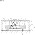
- FIG. 1 illustrates a schematic cross sectional view accounting a problem of an electronic device that includes a high-frequency-wave semiconductor device 28 mounted face down.
- a circuit portion 14 is provided on a substrate 10 such as a GaAs substrate.
- a metal bump 16 is provided on a face on which the circuit portion 14 is provided, the metal bump 16 being a face-down mounting portion electrically coupled to the circuit portion 14.
- the semiconductor device 28 is mounted in a package 20 as a substrate mounted portion.
- the package 20 includes a package substrate 22 having a wiring pattern and a chassis 24 covered with metal.
- the metal bump 16 provided on the substrate 10 is coupled to a wiring pattern (not shown) of the package substrate 22.
- a face of the substrate 10, on which the circuit portion 14 is provided, is mounted face down on the package substrate 22. That is, the substrate 10 is mounted face down in the package 20.
- the substrate 10 and the package 20 are coupled to each other through the metal bump 16. That is, the substrate 10 is mounted flip-chip in the package 20.
- the package 20 has a terminal (not shown) outside thereof.
- the wiring pattern is electrically coupled to the terminal. Air or an inert gas 26 is filled in the package 20.
- Z indicates the impedance of the medium.
- ⁇ 0 indicates a dielectric constant in a vacuum (air).
- ⁇ 0 indicates a magnetic permeability in the vacuum.
- ⁇ indicates a relative dielectric constant,
- ⁇ indicates a relative magnetic permeability.
- a reflection coefficient, in a case where a high frequency wave propagates from a medium 1 to a medium 2, is shown as following Expression 2.
- S Z L ⁇ Z C Z L + Z C
- S indicates a reflection coefficient.
- Z C indicates an impedance of the medium 1.
- Z L indicates an impedance of the medium 2.
- the resistance component of the impedance in a vacuum is approximately 377 ⁇ .
- Air or an inert gas 26 is filled in the package 20.
- the impedance does not differ in cases of in a vacuum, air, an inert gas or other gas.
- the package 20 may be vacuum-sealed or may be filled with a gas.
- the impedance in the vacuum is used as the impedance in air.
- the relative dielectric constant of the substrate 10 is, for example, 13.1 in a case where the substrate 10 is composed of GaAs.
- the resistance component of the impedance of the GaAs substrate is 104 ⁇ .
- a high frequency wave 51 from the circuit portion 14 is reflected at the back face of the substrate 10.
- the reflected wave is referred to a high frequency wave 52.
- the high frequency wave 52 goes to the circuit portion 14.
- the rest of the high frequency wave 51 transmits the interface between the substrate 10 and the air 26.
- the transmission wave is referred to a high frequency wave 53.
- Approximately 100% of the high frequency wave 53 is reflected at the upper face of the chassis 24.
- the reflected wave is referred to a high frequency wave 54.
- a part of the high frequency wave 54 is reflected at the interface between the air 26 and the substrate 10.
- the reflected wave is referred to a high frequency wave 56.
- the rest of the high frequency wave 54 transmits the interface between the air 26 and the substrate 10, and goes to the circuit portion 14 as a high frequency wave 55.
- the most part of the high frequency wave 51, the high frequency waves 52 and 55 goes to the circuit portion 14 as a reflected wave.
- FIG. 2 illustrates a cross sectional view of an electronic device for examination.
- the electronic device includes the high-frequency-wave semiconductor device 28.
- the conductive layer 12 is provided at a face of the substrate 10 (a back face) that is opposite side of a face on which the circuit portion 14 is provided in the electronic device in FIG. 2 .
- the same components have the same reference numerals in order to avoid a duplicated explanation.
- a sheet resistance of the conductive layer 12 is an impedance.
- the reflectivity of the high frequency wave from the circuit portion 14 at the interface between the substrate 10 and the conductive layer 12 is calculated with the Expression 1.
- the sheet resistance of the conductive layer 12 is approximately same as the resistance component of the impedance of the substrate 10, almost all of a high frequency wave 61 from the circuit portion 14 is not reflected at the interface between the substrate 10 and the conductive layer 12 as shown in FIG. 2 .
- the high frequency wave 61 is attenuated as transmitting the conductive layer 12. A part of the high frequency wave 61 is reflected at the interface between the conductive layer 12 and the air 26. The reflected wave is referred to a high frequency wave 62. The high frequency wave 62 is attenuated in the conductive layer 12. The rest of the high frequency wave 61 transmits the interface between the conductive layer 12 and the air 26. The transmission wave is referred to a high frequency wave 63. The high frequency wave 63 is reflected at the chassis 24. The reflected wave is referred to a high frequency wave 64. A part of the high frequency wave 64 is reflected at the interface between the air 26 and the conductive layer 12. The reflected wave is referred to a high frequency wave 66.
- the rest of the high frequency wave 64 transmits the interface between the air 26 and the conductive layer 12.
- the transmission wave is referred to a high frequency wave 65.
- the high frequency wave 65 goes to the circuit portion 14. In this case, the high frequency wave 65 is attenuated in the conductive layer 12.
- the high frequency waves 62 and 65 transmit the conductive layer 12 twice and goes to the circuit portion 14. Therefore, the high frequency waves 62 and 65 are attenuated in the conductive layer 12.
- the inventor has thought that in the structure shown in FIG. 2 it is possible to restrain the affection of the reflected wave of the high frequency wave to the circuit portion 14, the high frequency wave being from the circuit portion 14. A description will be given of examples based on the principle.
- the manufacturing cost increases when the thickness of the conductive layer 12 is excessive.
- the electrical resistivity of the conductive layer 12 is important in order to effectively limit the reflection in the thin conductive layer 12.
- NiCr nickel-chrome
- TaN tantalum nitride
- ITO indium tin oxide
- a NiCr layer, a TaN layer and an ITO layer were used as the conductive layer 12.
- GaAs gallium arsenide
- Si silicon
- SiC silicon carbide
- sapphire Al 2 O 3
- GaN gallium nitride
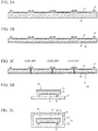
- FIG. 3A through FIG. 3E illustrate a cross sectional view of a semiconductor device showing a manufacturing process thereof, the semiconductor device being in accordance with one of the first examples.
- the substrate 10 is composed of GaAs and the conductive layer 12 is composed of NiCr in the semiconductor device.
- a 76 GHz amplifier as the circuit portion 14 was manufactured on the substrate 10 composed of GaAs.
- the metal bump 16 was formed electrically coupled to the circuit portion 14.
- the metal bump 16 was formed by plating with Au.
- the back face of the substrate 10 was grinded.
- a NiCr layer as the conductive layer 12 was formed on the back face of the substrate 10 by a sputtering.
- the substrate 10 and the conductive layer 12 were cut-off with a dicing into a chip as the high-frequency-wave semiconductor device 28.
- the conductive layer 12 is electrically separated from the circuit portion 14.
- the NiCr layer may be formed by an evaporation method in FIG. 3B .
- the semiconductor device 28 was mounted face down on the package substrate 22 so that the metal bump 16 was electrically coupled to the wiring pattern of the package substrate 22.
- the chassis 24 was bonded to the package substrate 22.
- the package 20 was filled with air 26.
- the conductive layer 12 is not coupled to the package 20. That is, the conductive layer 12 is electrically separated from the package 20. Thus the conductive layer 12 is electrically shut away. It is possible to restrain that the capacitance of the circuit portion 14 increases.
- the conductive layer 12 is electrically separated from the grand of the package 20. Thus it is possible to further restrain that the capacitance of the circuit portion 14 increases.
- the electronic device in accordance with the first example was manufactured, the electronic device having the substrate 10 composed of GaAs and the conductive layer 12 composed of NiCr.
- the package 20 may be filled with the inert gas. In this case, it is possible to restrain an oxidization of the semiconductor device 28.
- the electronic device having the GaAs substrate and the NiCr substrate was used and an isolation quality at 76 GHz was measured.
- the isolation quality is referred to an electrical power ratio of output signals: one of the signals is an output signal in a case where an input signal at 76 GHz is fed into the amplifier and a power supply voltage is applied to the amplifier, the other is an output signal in a case where the input signal is fed into the amplifier and the power supply voltage is not applied to the amplifier.
- a vector network analyzer was used for measuring the isolation quality. When the reflectivity of the high frequency wave from the circuit portion 14 is high, the reflection wave of the input signal is output as an output signal in the case where the power supply voltage is not applied to the amplifier. And the isolation quality is degraded.
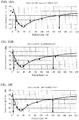
- FIG. 4A illustrates the isolation quality according to the thickness of the conductive layer 12.
- the dots indicate a measured value.
- the curved line is a line where the measured values are fitted.
- the isolation quality of the electronic device in accordance with the first example is most favorable when the thickness of the conductive layer 12 is approximately 18 nm, and is reduced when the thickness is thinner or thicker. It is thought that the isolation quality is most favorable when the thickness of the conductive layer 12 is a value in a case where the sheet resistance of the conductive layer 12 corresponds to the resistance component of the impedance of the substrate 10. When the thickness of the conductive layer 12 gets thicker, the isolation quality is approximately constant of -40 dBm.
- the thickness of the conductive layer 12 is within a range where the isolation quality is less than -40 dBm, in order to limit the reflection of the high frequency wave. Therefore, it is preferable that the thickness of the conductive layer 12 provided on the back face of the GaAs substrate is 4 nm to 70 nm in order to limit the reflection of the high frequency wave. It is preferable that the thickness of the conductive layer 12 is 6 nm to 36 nm in order to reduce the isolation quality less than -50 dBm. That is, the thickness of the conductive layer 12 is preferably 1/4 to 4 times, more preferably 1/3 to 2 times, of the thickness in the case where the sheet resistance of the conductive layer 12 corresponds to the resistance component of the impedance of the substrate 10.
- FIG. 5 illustrates a measured isolation quality in a case where the input signals fed into the amplifier are of 60 GHz and 80 GHz.
- the isolation quality approximately corresponds to that in a case of FIG. 4A , even if the frequency of the input signal is changed.
- FIG. 6 illustrates a block diagram of a 76 GHz car radar including the amplifier having the GaAs substrate and the NiCr layer in accordance with the first example.
- a 76 GHz signal generated in an oscillator 30 is amplified in a transmitter amplifier 36, and is output from a transmission antenna 38 as a high frequency wave of 76 GHz.
- the high frequency wave is, for example, reflected at a car 42 and fed into a reception antenna 40.
- a received signal is amplified in a receiver amplifier 34 and is converted into an intermediate frequency in a mixer 32.
- a low-intensity high frequency wave being pretty close to the emitted high frequency wave, is detected and amplified. Therefore, in a case where the circuit portion 14 has a circuit using a high frequency wave used for the radar system, a high frequency wave reflected at the car 42 is reflected in the package, goes to the circuit portion 14, and is indistinguishable from a high frequency wave that is emitted from the circuit portion 14. And a malfunction is possibly occurred. It is thus possible to restrain the malfunction when the embodiment is applied to the circuit.
- a high frequency wave emitted from the transmitter amplifier 36 is reflected in the package and goes to the receiver amplifier 34 in a case where the transmitter amplifier 36 and the receiver amplifier 34 are provided on a GaAs substrate as an MMIC 31, that is, in a case where the circuit portion 14 has a transmission amplifier and a reception amplifier of the radar system. Therefore, the malfunction is occurred easily. However, it is possible to restrain the malfunction if the embodiment is applied.
- the isolation qualities of the amplifiers were measured, the amplifiers having a NiCr layer, a TaN layer or an ITO layer provided on a GaAs substrate, a Si substrate, a SiC substrate, a sapphire substrate or a GaN substrate. It is thought that other amplifiers not having the GaAs substrate and the NiCr layer has little dependence on frequency of an input signal in the isolation quality, as is in the case of FIG. 5 . So, the isolation qualities were measured in cases where an input signal of 76 GHz is fed into the amplifier provided on the GaAs substrate and an input signal of 2 GHz is fed into the amplifiers provided on other substrates.
- FIG. 4B, FIG. 4C , FIG. 7A and FIG. 7B illustrate an isolation quality when the NiCr layer is provided on the Si substrate, the SiC substrate, the sapphire substrate and the GaN substrate.
- the isolation qualities are less than -40 dBm when the thickness of the NiCr layer is 3 nm to 65 nm, 3 nm to 63 nm, 3 nm to 63 nm and 3 nm to 68 nm in the cases of the Si substrate, the SiC substrate, the sapphire substrate and the GaN substrate respectively.
- FIG. 8A, FIG. 8B, FIG. 8C , FIG. 9A and FIG. 9B illustrate an isolation quality of the amplifiers in the cases where the TaN layer is provided on the GaAs substrate, Si substrate, the SiC substrate, the sapphire substrate and the GaN substrate respectively.
- the isolation qualities are less than -40 dBm when the thickness of the TaN layer is 10 nm to 200 nm, 10 nm to 180 nm, 7 nm to 160 nm, 7 nm to 160 nm and 10 nm to 180 nm in the cases of the GaAs substrate, the Si substrate, the SiC substrate, the sapphire substrate and the GaN substrate respectively.
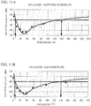
- FIG. 10A, FIG. 10B, FIG. 10C , FIG. 11A and FIG. 11B illustrate an isolation quality of the amplifiers in the cases where the ITO layer is provided on the GaAs substrate, Si substrate, the SiC substrate, the sapphire substrate and the GaN substrate respectively.
- the isolation qualities are less than -40 dBm when the thickness of the ITO layer is 10 nm to 160 nm, 5 nm to 140 nm, 5 nm to 140 nm, 5 nm to 140 nm and 5 nm to 140 nm in the cases of the GaAs substrate, the Si substrate, the SiC substrate, the sapphire substrate and the GaN substrate respectively.
- the thickness of the conductive layer 12 is 1/4 to 4 times of the thickness in the case where the sheet resistance of the conductive layer 12 corresponds to the resistance component of the impedance of the substrate 10. It is preferable that the thickness of the conductive layer 12 is 1/3 to 2 times of the thickness in the case. And the thickness of the conductive layer 12 may be 3 nm to 200 nm, when the resistivity of the conductive layer 12 is 1.0 X 10 -6 ⁇ m to 2.5 X 10 -6 ⁇ m. It is possible to restrain the separation of the conductive layer 12, the increase of the manufacturing cost and the difficulty of controlling the thickness.
- the conductive layer 12 is effective when the conductive layer 12 is provided on at least a part of the back face of the substrate 10. And it is possible to effectively restrain the reflection at the interface between the substrate 10 and the conductive layer 12 when the conductive layer 12 is provided on the whole area of the back face of the substrate 10. And it is possible to more effectively restrain the reflection at the interface between the substrate 10 and the conductive layer 12 when the conductive layer 12 is provided directly on the substrate 10.
- the package 20 is effective when the substrate 10 can be mounted thereon.
- the package 20 may be a multilayer wiring substrate as a motherboard.
Landscapes
- Semiconductor Integrated Circuits (AREA)
- Structure Of Printed Boards (AREA)
Description
- This invention generally relates to an electronic device and a semiconductor device, and in particular, relates to an electronic device and a semiconductor device using a high frequency wave in a package.
- Recently, radio wave such as a microwave or a milliwave (high frequency wave) is used in a communication field including a cellular phone. The high frequency wave is used for a radar or the like measuring a distance between two cars. A high-frequency-wave semiconductor device is often downsized, and is often mounted face down in order to restrain a loss of a signal. The high-frequency-wave semiconductor device is used for an electronic device using a high frequency wave.
- The face-down mounting is a method of mounting a face, where a circuit portion using a high frequency wave is provided, on a wiring pattern of a package acting as a substrate mounted portion. Hereinafter, the face, where the circuit portion using the high frequency wave is provided, is referred to a front face and, a face backside of the front face is referred to a back face. The circuit portion is a circuit where an active device or a passive device are provided, the active device including such as a transistor or a diode, the passive device including such as a capacitor, a diode, or a wiring pattern. Or the circuit portion is a portion where a stand-alone device is provided.
- In a high-frequency-wave semiconductor device, there are problems caused by a high frequency wave generated in the circuit portion. Japanese Patent Application Publication No.
9-102705 2005-217222 - In an electronic device having a high-frequency-wave semiconductor device, a high frequency wave generated in the circuit portion is reflected in a package and fed into the circuit portion as a reflection wave. In particular, a high frequency wave in a
range 60 GHz to 80 GHz goes straight. And a reflection wave reflected in the package interferes a signal in the circuit portion. The high frequency wave from a circuit portion, which is provided on a substrate mounted face down, is reflected at a back face of the substrate. Thus, in a structure of theconventional embodiment 1, it is not possible to restrain that the high frequency wave emitted from the circuit portion is reflected at an interface between the substrate and the air and goes to the circuit portion. In a structure of theconventional embodiment 2, the high frequency wave is reflected at an interface between the substrate and the soft magnetic material. Thus, it is not sufficiently restrained that the high frequency wave emitted from the circuit portion is reflected and goes to the circuit portion. In addition, it is necessary to form a soft magnetic material of a few hundreds µm on a back face of the substrate. And the manufacturing cost increases.
US 2002/0030267 A1 discloses a compound semiconductor device configured to reduce the restriction on the arrangement of elements constituting the integrated circuit, and also suppressing variation in an inductance component in a high frequency transmission system.
FR 2784768 A1 WO 98/20561 A1 - The present invention provides a semiconductor device mounted face down and an electronic device including the semiconductor device that are capable of limiting a reflection of a high frequency wave generated in a circuit portion at a back face of a substrate.
- The invention is defined in any independent claim. Optional embodiments are set out in the dependent claims.
- With the above-mentioned configuration, it is possible to limit a reflection of a high frequency wave at an interface between the substrate and the conductive layer, in a high-frequency-wave electronic device mounted face down. It is possible to form the conductive layer easily, and to reduce a manufacturing cost.
- According to another aspect of the present invention, which is not specifically claimed, there is provided an electronic device including a substrate, a conductive layer and a substrate mounted portion. The substrate has a circuit portion used from 60 GHz to 80 GHz. The conductive layer is provided directly on a face of the substrate that is opposite side of the circuit portion. The face having the circuit portion of the substrate is mounted face down on the substrate mounted portion. A thickness of the conductive layer is a thickness where a sheet resistance of the conductive layer is 1/4 to 4 times of a resistance component of an impedance of the substrate.
- With the above-mentioned configuration, it is possible to limit a reflection of a high frequency wave at an interface between the substrate and the conductive layer, in a high-frequency-wave electronic device mounted face down.
- According to another aspect of the present invention, which is not specifically claimed, there is provided a semiconductor device including a substrate, a conductive layer and a face-down mounting portion. The substrate has a circuit portion used from 60 GHz to 80 GHz. The conductive layer is provided directly on a face of the substrate that is opposite side of the circuit portion. The face-down mounting portion for a face-down mounting is provided on the face having the circuit portion of the substrate. The substrate is one of a GaAs substrate, a Si substrate, a SiC substrate, a sapphire substrate and a GaN substrate. The conductive layer is one of a NiCr layer of 4 nm to 70 nm thickness, a TaN layer of 10 nm to 200 nm thickness, an ITO layer of 10 nm to 160 nm thickness, in a case where the substrate is the GaAs substrate. The conductive layer is one of a NiCr layer of 3 nm to 65 nm thickness, a TaN layer of 10 nm to 180 nm thickness, an ITO layer of 5 nm to 140 nm thickness, in a case where the substrate is the Si substrate. The conductive layer is one of a NiCr layer of 3 nm to 63 nm thickness, a TaN layer of 7 nm to 160 nm thickness, an ITO layer of 5 nm to 140 nm thickness, in a case where the substrate is the SiC substrate. The conductive layer is one of a NiCr layer of 3 nm to 63 nm thickness, a TaN layer of 7 nm to 160 nm thickness, an ITO layer of 5 nm to 140 nm thickness, in a case where the substrate is the sapphire substrate. The conductive layer is one of a NiCr layer of 3 nm to 68 nm thickness, a TaN layer of 10 nm to 180 nm thickness, an ITO layer of 5 nm to 140 nm thickness, in a case where the substrate is the GaN substrate.
- With the above-mentioned configuration, it is possible to limit a reflection of a high frequency wave at an interface between the substrate and the conductive layer, in a high-frequency-wave semiconductor device to be 9mounted face down. It is possible to form the conductive layer easily, and to reduce a manufacturing cost.
- According to another aspect of the present invention, which is not specifically claimed, there is provided a semiconductor device including a substrate, a conductive layer and a face-down mounting portion. The substrate has a circuit portion used from 60 GHz to 80 GHz. The conductive layer is provided directly on a face of the substrate that is opposite side of the circuit portion. The face-down mounting portion for a face-down mounting is provided on the face having the circuit portion of the substrate. A thickness of the conductive layer is a thickness where a sheet resistance of the conductive layer is 1/4 to 4 times of a resistance component of an impedance of the substrate.
- With the above-mentioned configuration, it is possible to limit a reflection of a high frequency wave at an interface between the substrate and the conductive layer, in a high-frequency-wave semiconductor device mounted face down.
- Preferred embodiments of the present invention will be described in detail with reference to the following drawings, wherein:
-
FIG. 1 illustrates a schematic cross sectional view accounting a problem of a high-frequency-wave semiconductor device mounted face down; -
FIG. 2 illustrates a principle of the invention and a cross sectional view ofFIG. 1 ; -
FIG. 3A through FIG. 3E illustrate a cross sectional view of a semiconductor device in accordance with a first example showing a manufacturing process thereof; -
FIG. 4A through FIG. 4C illustrate an isolation quality of amplifiers when a NiCr layer is provided on a GaAs substrate, a Si substrate and a SiC substrate respectively; -
FIG. 5 illustrates an isolation quality of an amplifier at each of frequencies in a case where a NiCr layer is provided on a GaAs substrate; -
FIG. 6 illustrates a block diagram in a case where a NiCr layer is provided on a GaAs substrate; -
FIG. 7A and FIG. 7B illustrate an isolation quality of amplifiers when a NiCr layer is provided on a sapphire substrate and a GaN substrate respectively; -
FIG. 8A through FIG. 8C illustrate an isolation quality of amplifiers in cases where a TaN layer is provided on a GaAs substrate, a Si substrate and a SiC substrate respectively; -
FIG. 9A and FIG. 9B illustrate an isolation quality of amplifiers in cases where a TaN layer is provided on a sapphire substrate and a GaN substrate respectively; -
FIG. 10A through FIG. 10C illustrate an isolation quality of amplifiers in cases where an ITO layer is provided on a GaAs substrate, a Si substrate and a SiC substrate respectively; and -
FIG. 11A and FIG. 11B illustrate an isolation quality of amplifiers in cases where an ITO layer is provided on a sapphire substrate and a GaN substrate respectively. - A description will now be given, with reference to the accompanying drawings, of embodiments of the present invention.
-
FIG. 1 illustrates a schematic cross sectional view accounting a problem of an electronic device that includes a high-frequency-wave semiconductor device 28 mounted face down. In thesemiconductor device 28, acircuit portion 14 is provided on asubstrate 10 such as a GaAs substrate. Ametal bump 16 is provided on a face on which thecircuit portion 14 is provided, themetal bump 16 being a face-down mounting portion electrically coupled to thecircuit portion 14. Thesemiconductor device 28 is mounted in apackage 20 as a substrate mounted portion. Thepackage 20 includes apackage substrate 22 having a wiring pattern and achassis 24 covered with metal. Themetal bump 16 provided on thesubstrate 10 is coupled to a wiring pattern (not shown) of thepackage substrate 22. A face of thesubstrate 10, on which thecircuit portion 14 is provided, is mounted face down on thepackage substrate 22. That is, thesubstrate 10 is mounted face down in thepackage 20. Thesubstrate 10 and thepackage 20 are coupled to each other through themetal bump 16. That is, thesubstrate 10 is mounted flip-chip in thepackage 20. Thepackage 20 has a terminal (not shown) outside thereof. The wiring pattern is electrically coupled to the terminal. Air or aninert gas 26 is filled in thepackage 20. - A description will be given of a reflection at a back face of the
substrate 10 of the electronic device shown inFIG. 1 . An impedance in a medium such as thesubstrate 10 is shown as followingExpression 1.
- Here, "Z" indicates the impedance of the medium. "ε0" indicates a dielectric constant in a vacuum (air). "µ0" indicates a magnetic permeability in the vacuum. "ε" indicates a relative dielectric constant, "µ" indicates a relative magnetic permeability.
- A reflection coefficient, in a case where a high frequency wave propagates from a medium 1 to a
medium 2, is shown as followingExpression 2.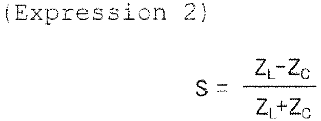
- Here, "S" indicates a reflection coefficient. "ZC" indicates an impedance of the
medium 1. "ZL" indicates an impedance of themedium 2. - The resistance component of the impedance in a vacuum is approximately 377 Ω. Air or an
inert gas 26 is filled in thepackage 20. The impedance does not differ in cases of in a vacuum, air, an inert gas or other gas. Thepackage 20 may be vacuum-sealed or may be filled with a gas. The impedance in the vacuum is used as the impedance in air. - A description will be given supposing that the
package 20 is filled with air. The relative dielectric constant of thesubstrate 10 is, for example, 13.1 in a case where thesubstrate 10 is composed of GaAs. In this case, the resistance component of the impedance of the GaAs substrate is 104 Ω. These values are assigned to the parameters of theExpression 2. And it is resulted that approximately 50% of the high frequency wave propagating into air from the GaAs substrate is reflected at an interface between thesubstrate 10 and theair 26. - Thus approximately 50% of a
high frequency wave 51 from thecircuit portion 14 is reflected at the back face of thesubstrate 10. The reflected wave is referred to ahigh frequency wave 52. Thehigh frequency wave 52 goes to thecircuit portion 14. The rest of thehigh frequency wave 51 transmits the interface between thesubstrate 10 and theair 26. The transmission wave is referred to ahigh frequency wave 53. Approximately 100% of thehigh frequency wave 53 is reflected at the upper face of thechassis 24. The reflected wave is referred to ahigh frequency wave 54. A part of thehigh frequency wave 54 is reflected at the interface between theair 26 and thesubstrate 10. The reflected wave is referred to ahigh frequency wave 56. The rest of thehigh frequency wave 54 transmits the interface between theair 26 and thesubstrate 10, and goes to thecircuit portion 14 as ahigh frequency wave 55. As mentioned above, the most part of thehigh frequency wave 51, the high frequency waves 52 and 55, goes to thecircuit portion 14 as a reflected wave. - There is a method of forming a thick
conductive layer 12 on the back face of thesubstrate 10, beside the methods in accordance with theconventional embodiments conductive layer 12 to be thick causes the increase of the manufacturing cost. So, it is examined whether a thin conductive layer limits the reflection of the high frequency wave effectively. -
FIG. 2 illustrates a cross sectional view of an electronic device for examination. The electronic device includes the high-frequency-wave semiconductor device 28. Being different fromFIG. 1 , theconductive layer 12 is provided at a face of the substrate 10 (a back face) that is opposite side of a face on which thecircuit portion 14 is provided in the electronic device inFIG. 2 . The same components have the same reference numerals in order to avoid a duplicated explanation. - It is supposed that a sheet resistance of the
conductive layer 12 is an impedance. And the reflectivity of the high frequency wave from thecircuit portion 14 at the interface between thesubstrate 10 and theconductive layer 12 is calculated with theExpression 1. When the sheet resistance of theconductive layer 12 is approximately same as the resistance component of the impedance of thesubstrate 10, almost all of ahigh frequency wave 61 from thecircuit portion 14 is not reflected at the interface between thesubstrate 10 and theconductive layer 12 as shown inFIG. 2 . - The
high frequency wave 61 is attenuated as transmitting theconductive layer 12. A part of thehigh frequency wave 61 is reflected at the interface between theconductive layer 12 and theair 26. The reflected wave is referred to ahigh frequency wave 62. Thehigh frequency wave 62 is attenuated in theconductive layer 12. The rest of thehigh frequency wave 61 transmits the interface between theconductive layer 12 and theair 26. The transmission wave is referred to ahigh frequency wave 63. Thehigh frequency wave 63 is reflected at thechassis 24. The reflected wave is referred to ahigh frequency wave 64. A part of thehigh frequency wave 64 is reflected at the interface between theair 26 and theconductive layer 12. The reflected wave is referred to ahigh frequency wave 66. The rest of thehigh frequency wave 64 transmits the interface between theair 26 and theconductive layer 12. The transmission wave is referred to ahigh frequency wave 65. Thehigh frequency wave 65 goes to thecircuit portion 14. In this case, thehigh frequency wave 65 is attenuated in theconductive layer 12. - As mentioned above, the high frequency waves 62 and 65 transmit the
conductive layer 12 twice and goes to thecircuit portion 14. Therefore, the high frequency waves 62 and 65 are attenuated in theconductive layer 12. The inventor has thought that in the structure shown inFIG. 2 it is possible to restrain the affection of the reflected wave of the high frequency wave to thecircuit portion 14, the high frequency wave being from thecircuit portion 14. A description will be given of examples based on the principle. - The manufacturing cost increases when the thickness of the
conductive layer 12 is excessive. The electrical resistivity of theconductive layer 12 is important in order to effectively limit the reflection in the thinconductive layer 12. NiCr (nickel-chrome), TaN (tantalum nitride) and ITO (indium tin oxide) having a resistivity of 1. 0X 10-6 Ωm, 2.5 X 10⁻⁶ Ωm and 2.0 X 10⁻⁶ Ωm respectively were selected, as a conductive material having a resistivity of approximately 1.0 X 10⁻⁶ Ωm. A NiCr layer, a TaN layer and an ITO layer were used as theconductive layer 12. A gallium arsenide (GaAs) substrate, a silicon (Si) substrate, a silicon carbide (SiC) substrate, a sapphire (Al2O3) substrate and a gallium nitride (GaN) substrate having a relative dielectric permeability of 13.1, 10.9, 10, 10 and 12.2 respectively were used as thesubstrate 10. And an amplifier was manufactured. -
FIG. 3A through FIG. 3E illustrate a cross sectional view of a semiconductor device showing a manufacturing process thereof, the semiconductor device being in accordance with one of the first examples. Thesubstrate 10 is composed of GaAs and theconductive layer 12 is composed of NiCr in the semiconductor device. - As shown in
FIG. 3A , a 76 GHz amplifier as thecircuit portion 14 was manufactured on thesubstrate 10 composed of GaAs. Themetal bump 16 was formed electrically coupled to thecircuit portion 14. Themetal bump 16 was formed by plating with Au. As shown inFIG. 3B , the back face of thesubstrate 10 was grinded. And a NiCr layer as theconductive layer 12 was formed on the back face of thesubstrate 10 by a sputtering. - As shown in
FIG. 3C , thesubstrate 10 and theconductive layer 12 were cut-off with a dicing into a chip as the high-frequency-wave semiconductor device 28. In thesemiconductor device 28, theconductive layer 12 is electrically separated from thecircuit portion 14. Thus theconductive layer 12 is electrically shut away. And it is restrained that the capacitance of thecircuit portion 14 increases. The NiCr layer may be formed by an evaporation method inFIG. 3B . - As shown in
FIG. 3D , thesemiconductor device 28 was mounted face down on thepackage substrate 22 so that themetal bump 16 was electrically coupled to the wiring pattern of thepackage substrate 22. As shown inFIG. 3E , thechassis 24 was bonded to thepackage substrate 22. Thepackage 20 was filled withair 26. Theconductive layer 12 is not coupled to thepackage 20. That is, theconductive layer 12 is electrically separated from thepackage 20. Thus theconductive layer 12 is electrically shut away. It is possible to restrain that the capacitance of thecircuit portion 14 increases. Theconductive layer 12 is electrically separated from the grand of thepackage 20. Thus it is possible to further restrain that the capacitance of thecircuit portion 14 increases. With the processes, the electronic device in accordance with the first example was manufactured, the electronic device having thesubstrate 10 composed of GaAs and theconductive layer 12 composed of NiCr. Thepackage 20 may be filled with the inert gas. In this case, it is possible to restrain an oxidization of thesemiconductor device 28. - The electronic device having the GaAs substrate and the NiCr substrate was used and an isolation quality at 76 GHz was measured. In this case, the thickness of the NiCr layer as the
conductive layer 12 was changed. The isolation quality is referred to an electrical power ratio of output signals: one of the signals is an output signal in a case where an input signal at 76 GHz is fed into the amplifier and a power supply voltage is applied to the amplifier, the other is an output signal in a case where the input signal is fed into the amplifier and the power supply voltage is not applied to the amplifier. A vector network analyzer was used for measuring the isolation quality. When the reflectivity of the high frequency wave from thecircuit portion 14 is high, the reflection wave of the input signal is output as an output signal in the case where the power supply voltage is not applied to the amplifier. And the isolation quality is degraded. -
FIG. 4A illustrates the isolation quality according to the thickness of theconductive layer 12. The dots indicate a measured value. The curved line is a line where the measured values are fitted. As shown inFIG. 4A , the isolation quality of the electronic device in accordance with the first example is most favorable when the thickness of theconductive layer 12 is approximately 18 nm, and is reduced when the thickness is thinner or thicker. It is thought that the isolation quality is most favorable when the thickness of theconductive layer 12 is a value in a case where the sheet resistance of theconductive layer 12 corresponds to the resistance component of the impedance of thesubstrate 10. When the thickness of theconductive layer 12 gets thicker, the isolation quality is approximately constant of -40 dBm. - Accordingly, it is necessary that the thickness of the
conductive layer 12 is within a range where the isolation quality is less than -40 dBm, in order to limit the reflection of the high frequency wave. Therefore, it is preferable that the thickness of theconductive layer 12 provided on the back face of the GaAs substrate is 4 nm to 70 nm in order to limit the reflection of the high frequency wave. It is preferable that the thickness of theconductive layer 12 is 6 nm to 36 nm in order to reduce the isolation quality less than -50 dBm. That is, the thickness of theconductive layer 12 is preferably 1/4 to 4 times, more preferably 1/3 to 2 times, of the thickness in the case where the sheet resistance of theconductive layer 12 corresponds to the resistance component of the impedance of thesubstrate 10. -
FIG. 5 illustrates a measured isolation quality in a case where the input signals fed into the amplifier are of 60 GHz and 80 GHz. As shown inFIG. 5 , the isolation quality approximately corresponds to that in a case ofFIG. 4A , even if the frequency of the input signal is changed. There is little dependence on frequency, in the thickness of theconductive layer 12 for limiting the reflection of the high frequency wave. It is possible to limit the reflection of the high frequency wave at the interface between thesubstrate 10 and theconductive layer 12, in a case where thecircuit portion 14 uses the high frequency waves within arange 60 GHz to 80 GHz. -
FIG. 6 illustrates a block diagram of a 76 GHz car radar including the amplifier having the GaAs substrate and the NiCr layer in accordance with the first example. A 76 GHz signal generated in anoscillator 30 is amplified in atransmitter amplifier 36, and is output from atransmission antenna 38 as a high frequency wave of 76 GHz. The high frequency wave is, for example, reflected at acar 42 and fed into areception antenna 40. A received signal is amplified in areceiver amplifier 34 and is converted into an intermediate frequency in amixer 32. - In the radar system mentioned above, a low-intensity high frequency wave, being pretty close to the emitted high frequency wave, is detected and amplified. Therefore, in a case where the
circuit portion 14 has a circuit using a high frequency wave used for the radar system, a high frequency wave reflected at thecar 42 is reflected in the package, goes to thecircuit portion 14, and is indistinguishable from a high frequency wave that is emitted from thecircuit portion 14. And a malfunction is possibly occurred. It is thus possible to restrain the malfunction when the embodiment is applied to the circuit. In particularly, a high frequency wave emitted from thetransmitter amplifier 36 is reflected in the package and goes to thereceiver amplifier 34 in a case where thetransmitter amplifier 36 and thereceiver amplifier 34 are provided on a GaAs substrate as anMMIC 31, that is, in a case where thecircuit portion 14 has a transmission amplifier and a reception amplifier of the radar system. Therefore, the malfunction is occurred easily. However, it is possible to restrain the malfunction if the embodiment is applied. - Similarly, the isolation qualities of the amplifiers were measured, the amplifiers having a NiCr layer, a TaN layer or an ITO layer provided on a GaAs substrate, a Si substrate, a SiC substrate, a sapphire substrate or a GaN substrate. It is thought that other amplifiers not having the GaAs substrate and the NiCr layer has little dependence on frequency of an input signal in the isolation quality, as is in the case of
FIG. 5 . So, the isolation qualities were measured in cases where an input signal of 76 GHz is fed into the amplifier provided on the GaAs substrate and an input signal of 2 GHz is fed into the amplifiers provided on other substrates. -
FIG. 4B, FIG. 4C ,FIG. 7A and FIG. 7B illustrate an isolation quality when the NiCr layer is provided on the Si substrate, the SiC substrate, the sapphire substrate and the GaN substrate. As shown in the figures, the isolation qualities are less than -40 dBm when the thickness of the NiCr layer is 3 nm to 65 nm, 3 nm to 63 nm, 3 nm to 63 nm and 3 nm to 68 nm in the cases of the Si substrate, the SiC substrate, the sapphire substrate and the GaN substrate respectively. -
FIG. 8A, FIG. 8B, FIG. 8C ,FIG. 9A and FIG. 9B illustrate an isolation quality of the amplifiers in the cases where the TaN layer is provided on the GaAs substrate, Si substrate, the SiC substrate, the sapphire substrate and the GaN substrate respectively. As shown in the figures, the isolation qualities are less than -40 dBm when the thickness of the TaN layer is 10 nm to 200 nm, 10 nm to 180 nm, 7 nm to 160 nm, 7 nm to 160 nm and 10 nm to 180 nm in the cases of the GaAs substrate, the Si substrate, the SiC substrate, the sapphire substrate and the GaN substrate respectively. -
FIG. 10A, FIG. 10B, FIG. 10C ,FIG. 11A and FIG. 11B illustrate an isolation quality of the amplifiers in the cases where the ITO layer is provided on the GaAs substrate, Si substrate, the SiC substrate, the sapphire substrate and the GaN substrate respectively. As shown in the figures, the isolation qualities are less than -40 dBm when the thickness of the ITO layer is 10 nm to 160 nm, 5 nm to 140 nm, 5 nm to 140 nm, 5 nm to 140 nm and 5 nm to 140 nm in the cases of the GaAs substrate, the Si substrate, the SiC substrate, the sapphire substrate and the GaN substrate respectively. - As mentioned above, in a case where the GaAs substrate is not used for the
substrate 10 and the NiCr layer is not used for theconductive layer 12, it is possible to limit the reflection of the high frequency wave emitted from thecircuit portion 14 when the thickness of theconductive layer 12 is 1/4 to 4 times of the thickness in the case where the sheet resistance of theconductive layer 12 corresponds to the resistance component of the impedance of thesubstrate 10. It is preferable that the thickness of theconductive layer 12 is 1/3 to 2 times of the thickness in the case. And the thickness of theconductive layer 12 may be 3 nm to 200 nm, when the resistivity of theconductive layer 12 is 1.0 X 10⁻⁶ Ωm to 2.5 X 10⁻⁶ Ωm. It is possible to restrain the separation of theconductive layer 12, the increase of the manufacturing cost and the difficulty of controlling the thickness. - The
conductive layer 12 is effective when theconductive layer 12 is provided on at least a part of the back face of thesubstrate 10. And it is possible to effectively restrain the reflection at the interface between thesubstrate 10 and theconductive layer 12 when theconductive layer 12 is provided on the whole area of the back face of thesubstrate 10. And it is possible to more effectively restrain the reflection at the interface between thesubstrate 10 and theconductive layer 12 when theconductive layer 12 is provided directly on thesubstrate 10. - The case, where the
package 20 is composed of thepackage substrate 22 and thechassis 24, is mentioned above. Thepackage 20 is effective when thesubstrate 10 can be mounted thereon. Thepackage 20 may be a multilayer wiring substrate as a motherboard. The case, where themetal bump 16 is a face-down mounting portion. The effect of the present invention is obtained when a face-down mounting portion is provided.
Claims (4)
- An electronic device comprising:a semiconductor device (28) including a substrate (10) having: a circuit portion (14) provided on a face and configured to use high frequency waves within a range of 60 GHz to 80 GHz and a metal bump (16) provided on this face which electrically couples to the circuit portion, and a conductive layer (12) provided directly on another face of the substrate (10) that is an opposite side of the substrate (10) to the face; anda package (20) including a package substrate (22) having a wiring pattern and a chassis (24) covered with metal, the package substrate (22) having the semiconductor device (28) mounted face down thereon, the metal bump (16) being coupled to the wiring pattern of the package substrate (22) and the chassis (24) facing the conductive layer (12), wherein:the substrate (10) is one of a GaAs substrate, a Si substrate, a SiC substrate, a sapphire substrate and a GaN substrate;the conductive layer (12) is one of a NiCr layer with a thickness of 4 nm to 70 nm, a TaN layer with a thickness of 10 nm to 200 nm, an ITO layer with a thickness of 10 nm to 160 nm, in a case where the substrate (10) is the GaAs substrate (10);the conductive layer (12) is one of a NiCr layer with a thickness of 3 nm to 65 nm, a TaN layer with a thickness of 10 nm to 180 nm, an ITO layer with a thickness of 5 nm to 140 nm, in a case where the substrate (10) is the Si substrate;the conductive layer (12) is one of a NiCr layer with a thickness of 3 nm to 63 nm, a TaN layer with a thickness of 7 nm to 160 nm, an ITO layer with a thickness of 5 nm to 140 nm, in a case where the substrate (10) is the SiC substrate;the conductive layer (12) is one of a NiCr layer with a thickness of 3 nm to 63 nm, a TaN layer with a thickness of 7 nm to 160 nm, an ITO layer with a thickness of 5 nm to 140 nm, in a case where the substrate (10) is the sapphire substrate; andthe conductive layer (12) is one of a NiCr layer with a thickness of 3 nm to 68 nm, a TaN layer with a thickness of 10 nm to 180 nm, an ITO layer with a thickness of 5 nm to 140 nm, in a case where the substrate (10) is the GaN substrate, andwherein the conductive layer (12) has a resistivity of 1.0 X 10⁻⁶ Ωm to 2.5 X 10⁻⁶ Ωm.
- The electronic device as claimed in claim 1, wherein the conductive layer (12) is provided on a whole area of the other face of the substrate (10) that is the opposite side of the face where the circuit portion (14) is provided.
- The electronic device as claimed in claim 1, wherein the conductive layer (12) is electrically separated from the substrate mounted portion (20).
- The electronic device as claimed in claim 1, wherein the conductive layer (12) is exposed to a vacuum (26) or a gas (26).
Applications Claiming Priority (1)
| Application Number | Priority Date | Filing Date | Title |
|---|---|---|---|
| JP2005362649A JP4680763B2 (en) | 2005-12-16 | 2005-12-16 | Electronic device and semiconductor device |
Publications (3)
| Publication Number | Publication Date |
|---|---|
| EP1801874A2 EP1801874A2 (en) | 2007-06-27 |
| EP1801874A3 EP1801874A3 (en) | 2013-05-01 |
| EP1801874B1 true EP1801874B1 (en) | 2019-03-06 |
Family
ID=37836771
Family Applications (1)
| Application Number | Title | Priority Date | Filing Date |
|---|---|---|---|
| EP06125848.9A Ceased EP1801874B1 (en) | 2005-12-16 | 2006-12-11 | Packaged electronic device and semiconductor device with a back-side conductive layer |
Country Status (3)
| Country | Link |
|---|---|
| US (1) | US7550831B2 (en) |
| EP (1) | EP1801874B1 (en) |
| JP (1) | JP4680763B2 (en) |
Families Citing this family (3)
| Publication number | Priority date | Publication date | Assignee | Title |
|---|---|---|---|---|
| US9576868B2 (en) * | 2012-07-30 | 2017-02-21 | General Electric Company | Semiconductor device and method for reduced bias temperature instability (BTI) in silicon carbide devices |
| JP5951156B2 (en) | 2014-03-26 | 2016-07-13 | 三菱電機株式会社 | Surface mount high frequency circuit |
| CN111146094B (en) * | 2019-12-04 | 2021-08-31 | 中国电子科技集团公司第十三研究所 | Gallium nitride power module packaging method and pressure device |
Family Cites Families (11)
| Publication number | Priority date | Publication date | Assignee | Title |
|---|---|---|---|---|
| JP3328102B2 (en) * | 1995-05-08 | 2002-09-24 | 松下電器産業株式会社 | Surface acoustic wave device and method of manufacturing the same |
| JPH09102705A (en) | 1995-10-06 | 1997-04-15 | Toshiba Corp | Microwave circuit device |
| JP4446292B2 (en) * | 1996-11-01 | 2010-04-07 | ローレンス バークレイ ラボラトリー | Photon sensing element and device using the same |
| JPH11195731A (en) * | 1997-10-30 | 1999-07-21 | Matsushita Electric Ind Co Ltd | Semiconductor device |
| FR2784768A1 (en) * | 1998-10-16 | 2000-04-21 | Schlumberger Ind Sa | Protecting integrated circuits on cards from the effects of electromagnetic radiation by using silica doped with Phosphorus or Boron or an irregular surface or metallic screening |
| JP3470052B2 (en) * | 1998-12-01 | 2003-11-25 | 京セラ株式会社 | Connection structure for high frequency components |
| JP3462166B2 (en) * | 2000-09-08 | 2003-11-05 | 富士通カンタムデバイス株式会社 | Compound semiconductor device |
| JP2005287055A (en) * | 2002-08-01 | 2005-10-13 | Matsushita Electric Ind Co Ltd | Transmission line and semiconductor integrated circuit device |
| JP4161911B2 (en) | 2004-01-30 | 2008-10-08 | ソニー株式会社 | Integrated circuit device |
| KR100855819B1 (en) * | 2004-10-08 | 2008-09-01 | 삼성전기주식회사 | MEMS package with metal sealing member |
| TWI241696B (en) * | 2004-11-26 | 2005-10-11 | Delta Electronics Inc | Chip package structure |
-
2005
- 2005-12-16 JP JP2005362649A patent/JP4680763B2/en not_active Expired - Fee Related
-
2006
- 2006-12-11 EP EP06125848.9A patent/EP1801874B1/en not_active Ceased
- 2006-12-13 US US11/637,878 patent/US7550831B2/en active Active
Non-Patent Citations (1)
| Title |
|---|
| None * |
Also Published As
| Publication number | Publication date |
|---|---|
| EP1801874A3 (en) | 2013-05-01 |
| US20070138622A1 (en) | 2007-06-21 |
| EP1801874A2 (en) | 2007-06-27 |
| US7550831B2 (en) | 2009-06-23 |
| JP2007165739A (en) | 2007-06-28 |
| JP4680763B2 (en) | 2011-05-11 |
Similar Documents
| Publication | Publication Date | Title |
|---|---|---|
| US12334902B2 (en) | Acoustic wave device with transverse mode suppression | |
| US12255613B2 (en) | Multi-layer piezoelectric substrate with conductive layer | |
| US20210058057A1 (en) | Multilayer piezoelectric substrate | |
| US12341487B2 (en) | Multilayer piezoelectric substrate for acoustic wave device | |
| US7750862B2 (en) | Broadband antenna for a transponder of a radio frequency identification system | |
| US20190229425A1 (en) | Combining Power Amplifiers at Millimeter Wave Frequencies | |
| US20220077840A1 (en) | Multi-layer piezoelectric substrate with controllable delta temperature coefficient of frequency | |
| US20120013421A1 (en) | Waveguide Structure, High Frequency Module Including Waveguide Structure, and Radar Apparatus | |
| US20050075080A1 (en) | Inter-chip and intra-chip wireless communications systems | |
| US8144059B2 (en) | Active dielectric resonator antenna | |
| US7566952B2 (en) | On-chip circuit pad structure | |
| JP2008089614A (en) | Radar sensor | |
| US8981872B2 (en) | Antenna duplexer with high GPS suppression | |
| US20230344407A1 (en) | Acoustic wave device having mass loading strip with buffer layer | |
| US7550831B2 (en) | Electronic device and semiconductor device | |
| EP3762995B1 (en) | Thin film surface mountable high frequency coupler | |
| US7304551B2 (en) | Branching filter and communication device | |
| US6642617B2 (en) | Semiconductor device | |
| US20250317123A1 (en) | Multi-layer piezoelectric substrate surface acoustic wave device with phase cancelling circuit | |
| US20250132744A1 (en) | Acoustic wave device and fabricating method thereof | |
| US20250211203A1 (en) | Fundamental tone mitigation for second overtone bulk acoustic wave resonator | |
| US20250274095A1 (en) | Multi-terminal bulk acoustic wave resonator utilizing overtone modes | |
| He et al. | Improvement of integrated dipole antenna performance using diamond for intra-chip wireless interconnection | |
| JPH0758586A (en) | High frequency circuit device | |
| Kikkawa et al. | Wireless Interconnection on Si LSI using Integrated Antenna |
Legal Events
| Date | Code | Title | Description |
|---|---|---|---|
| PUAI | Public reference made under article 153(3) epc to a published international application that has entered the european phase |
Free format text: ORIGINAL CODE: 0009012 |
|
| AK | Designated contracting states |
Kind code of ref document: A2 Designated state(s): AT BE BG CH CY CZ DE DK EE ES FI FR GB GR HU IE IS IT LI LT LU LV MC NL PL PT RO SE SI SK TR |
|
| AX | Request for extension of the european patent |
Extension state: AL BA HR MK YU |
|
| PUAL | Search report despatched |
Free format text: ORIGINAL CODE: 0009013 |
|
| AK | Designated contracting states |
Kind code of ref document: A3 Designated state(s): AT BE BG CH CY CZ DE DK EE ES FI FR GB GR HU IE IS IT LI LT LU LV MC NL PL PT RO SE SI SK TR |
|
| AX | Request for extension of the european patent |
Extension state: AL BA HR MK RS |
|
| RIC1 | Information provided on ipc code assigned before grant |
Ipc: H01L 23/552 20060101AFI20130325BHEP Ipc: H01L 23/04 20060101ALI20130325BHEP Ipc: H01L 23/66 20060101ALI20130325BHEP Ipc: H01L 23/20 20060101ALI20130325BHEP Ipc: H01L 23/10 20060101ALI20130325BHEP |
|
| 17P | Request for examination filed |
Effective date: 20131028 |
|
| RBV | Designated contracting states (corrected) |
Designated state(s): AT BE BG CH CY CZ DE DK EE ES FI FR GB GR HU IE IS IT LI LT LU LV MC NL PL PT RO SE SI SK TR |
|
| AKX | Designation fees paid |
Designated state(s): DE FR GB |
|
| 17Q | First examination report despatched |
Effective date: 20131211 |
|
| STAA | Information on the status of an ep patent application or granted ep patent |
Free format text: STATUS: EXAMINATION IS IN PROGRESS |
|
| GRAP | Despatch of communication of intention to grant a patent |
Free format text: ORIGINAL CODE: EPIDOSNIGR1 |
|
| STAA | Information on the status of an ep patent application or granted ep patent |
Free format text: STATUS: GRANT OF PATENT IS INTENDED |
|
| INTG | Intention to grant announced |
Effective date: 20180928 |
|
| RAP1 | Party data changed (applicant data changed or rights of an application transferred) |
Owner name: SUMITOMO ELECTRIC DEVICE INNOVATIONS, INC. |
|
| RIN1 | Information on inventor provided before grant (corrected) |
Inventor name: NUNOKAWA, MITSUJI |
|
| GRAS | Grant fee paid |
Free format text: ORIGINAL CODE: EPIDOSNIGR3 |
|
| GRAA | (expected) grant |
Free format text: ORIGINAL CODE: 0009210 |
|
| STAA | Information on the status of an ep patent application or granted ep patent |
Free format text: STATUS: THE PATENT HAS BEEN GRANTED |
|
| AK | Designated contracting states |
Kind code of ref document: B1 Designated state(s): DE FR GB |
|
| REG | Reference to a national code |
Ref country code: GB Ref legal event code: FG4D |
|
| REG | Reference to a national code |
Ref country code: DE Ref legal event code: R096 Ref document number: 602006057542 Country of ref document: DE |
|
| REG | Reference to a national code |
Ref country code: DE Ref legal event code: R097 Ref document number: 602006057542 Country of ref document: DE |
|
| PLBE | No opposition filed within time limit |
Free format text: ORIGINAL CODE: 0009261 |
|
| STAA | Information on the status of an ep patent application or granted ep patent |
Free format text: STATUS: NO OPPOSITION FILED WITHIN TIME LIMIT |
|
| 26N | No opposition filed |
Effective date: 20191209 |
|
| P01 | Opt-out of the competence of the unified patent court (upc) registered |
Effective date: 20230515 |
|
| PGFP | Annual fee paid to national office [announced via postgrant information from national office to epo] |
Ref country code: GB Payment date: 20231102 Year of fee payment: 18 |
|
| PGFP | Annual fee paid to national office [announced via postgrant information from national office to epo] |
Ref country code: FR Payment date: 20231108 Year of fee payment: 18 Ref country code: DE Payment date: 20231031 Year of fee payment: 18 |
|
| REG | Reference to a national code |
Ref country code: DE Ref legal event code: R119 Ref document number: 602006057542 Country of ref document: DE |
|
| GBPC | Gb: european patent ceased through non-payment of renewal fee |
Effective date: 20241211 |
|
| PG25 | Lapsed in a contracting state [announced via postgrant information from national office to epo] |
Ref country code: DE Free format text: LAPSE BECAUSE OF NON-PAYMENT OF DUE FEES Effective date: 20250701 |
|
| PG25 | Lapsed in a contracting state [announced via postgrant information from national office to epo] |
Ref country code: GB Free format text: LAPSE BECAUSE OF NON-PAYMENT OF DUE FEES Effective date: 20241211 |
|
| PG25 | Lapsed in a contracting state [announced via postgrant information from national office to epo] |
Ref country code: FR Free format text: LAPSE BECAUSE OF NON-PAYMENT OF DUE FEES Effective date: 20241231 |