EP1796212A1 - Patch antenna - Google Patents
Patch antenna Download PDFInfo
- Publication number
- EP1796212A1 EP1796212A1 EP06025245A EP06025245A EP1796212A1 EP 1796212 A1 EP1796212 A1 EP 1796212A1 EP 06025245 A EP06025245 A EP 06025245A EP 06025245 A EP06025245 A EP 06025245A EP 1796212 A1 EP1796212 A1 EP 1796212A1
- Authority
- EP
- European Patent Office
- Prior art keywords
- conductor
- short
- radiating
- feeding
- radiating conductor
- Prior art date
- Legal status (The legal status is an assumption and is not a legal conclusion. Google has not performed a legal analysis and makes no representation as to the accuracy of the status listed.)
- Granted
Links
- 239000004020 conductor Substances 0.000 claims abstract description 151
- 239000000758 substrate Substances 0.000 claims abstract description 19
- 230000000149 penetrating effect Effects 0.000 claims description 3
- 230000005284 excitation Effects 0.000 description 5
- 238000004519 manufacturing process Methods 0.000 description 5
- 230000005855 radiation Effects 0.000 description 5
- 230000010287 polarization Effects 0.000 description 4
- 238000009826 distribution Methods 0.000 description 3
- 238000000034 method Methods 0.000 description 3
- 230000001737 promoting effect Effects 0.000 description 3
- 238000010586 diagram Methods 0.000 description 2
- 230000005611 electricity Effects 0.000 description 2
- 230000002708 enhancing effect Effects 0.000 description 2
- 230000015572 biosynthetic process Effects 0.000 description 1
- 230000006866 deterioration Effects 0.000 description 1
Images

Classifications
-
- H—ELECTRICITY
- H01—ELECTRIC ELEMENTS
- H01Q—ANTENNAS, i.e. RADIO AERIALS
- H01Q9/00—Electrically-short antennas having dimensions not more than twice the operating wavelength and consisting of conductive active radiating elements
- H01Q9/04—Resonant antennas
- H01Q9/0407—Substantially flat resonant element parallel to ground plane, e.g. patch antenna
- H01Q9/0428—Substantially flat resonant element parallel to ground plane, e.g. patch antenna radiating a circular polarised wave
-
- H—ELECTRICITY
- H01—ELECTRIC ELEMENTS
- H01Q—ANTENNAS, i.e. RADIO AERIALS
- H01Q1/00—Details of, or arrangements associated with, antennas
- H01Q1/36—Structural form of radiating elements, e.g. cone, spiral, umbrella; Particular materials used therewith
- H01Q1/38—Structural form of radiating elements, e.g. cone, spiral, umbrella; Particular materials used therewith formed by a conductive layer on an insulating support
-
- H—ELECTRICITY
- H01—ELECTRIC ELEMENTS
- H01Q—ANTENNAS, i.e. RADIO AERIALS
- H01Q9/00—Electrically-short antennas having dimensions not more than twice the operating wavelength and consisting of conductive active radiating elements
- H01Q9/04—Resonant antennas
- H01Q9/0407—Substantially flat resonant element parallel to ground plane, e.g. patch antenna
- H01Q9/0421—Substantially flat resonant element parallel to ground plane, e.g. patch antenna with a shorting wall or a shorting pin at one end of the element
Definitions
- the present invention relates to a planar-feed-type patch antenna capable of feeding electricity to a radiating conductor in the same plane as the radiating conductor is disposed, and more particularly, it relates to a patch antenna operated as a circularly polarized antenna.
- a planar-feed-type patch antenna typically has a radiating conductor and an impedance matching circuit disposed on one surface of a dielectric substrate, and a ground conductor disposed on the other surface of the dielectric substrate in at least a region opposing the radiating conductor.
- a feed signal is applied to a certain position at an edge of the radiating conductor via the impedance matching circuit.
- the impedance matching circuit since the impedance matching circuit is provided in the configuration, the patch antenna may be consequently of large size.
- a patch antenna in which a pair of slits are formed at edges of the radiating conductor, and a feeding section is provided within a band-like region interposed between the slits, so that electricity may be fed directly to the feeding section (for example, see Japanese Unexamined Patent Application Publication No. 5-259731 , pages 2 to 4, Fig. 2).
- the above-mentioned known patch antenna is used for linear polarization, and impedance may be adjusted by properly determining the depth of the pair of slits sandwiching the feeding section. Accordingly, additional provision of the impedance matching circuit is not necessary, thereby promoting reduction in size of the patch antenna.
- the method of adjusting the impedance according to the formation of the slits at the edges of the radiating conductor would not cause any problem when it is applied to a linearly polarized antenna.
- the method when the method is applied to a circularly polarized antenna, it may be difficult to obtain a good axial ratio characteristic, inevitably causing deterioration in radiation gain.
- the known method when the known method is applied to the circularly polarized antenna, it is necessary to form slits not only in the vicinity of the feeding section of the radiating conductor for the impedance adjustment, but also at other edges extending in a direction orthogonal to the former slits, for compensation.
- an object of the present invention is to provide a planar-feed-type patch antenna for circular polarization providing a good axial ratio characteristic and being of reduced size.
- a patch antenna includes: a ground conductor; a radiating conductor which is loaded with a degeneracy splitting element and disposed so as to oppose the ground conductor with a predetermined distance therebetween; a feeding conductor which extends from the radiating conductor outward in the radial direction of the radiating conductor so that a tip of the feeding conductor functions as a feeding section; and a short-circuit conductor which is disposed to connect the radiating conductor to the ground conductor at a predetermined position in a region of the radiating conductor opposite to the feeding conductor.
- a 0 ⁇ impedance point, at which voltage becomes zero in feeding, is provided at a location deviated from the center of the radiating conductor and at which the radiating conductor is connected to the short-circuit conductor, and distributions of voltage and current would be largely different from those in a case where the short-circuit conductor is not provided. Accordingly, it is possible to set the feeding section with an impedance of 50 ⁇ in the feeding conductor extending outward from the radiating conductor.
- the number of the short-circuit conductors is appropriately determined on the basis of the location on the radiating conductor at which the short-circuit conductor is connected. For example, when the short-circuit conductor is connected to the radiating conductor at the predetermined position disposed on an extension of a line connecting the center of the radiating conductor and the feeding conductor, the short-circuit conductor is required to be provided only at this one location, thereby facilitating manufacturing.
- the short-circuit conductors are provided at these two locations, and accordingly, it becomes possible to adjust the resonance characteristics appropriately for both of the two excitation modes which are electrically and spatially orthogonal to each other, thereby further enhancing improvement of the axial ratio characteristic.
- the radiating conductor and the feeding conductor may be disposed on one surface of a dielectric substrate, whereas the ground conductor may be disposed on the other surface of the dielectric substrate, and the short-circuit conductor is provided in a through hole penetrating through the dielectric substrate.
- This configuration is preferable because it may provide a patch antenna having a simple structure and promoting mass production.
- the patch antenna according to the present invention it is possible to set the feeding section with the impedance of 50 ⁇ in the feeding conductor extending outward in the radial direction from the radiating conductor, by connecting the short-circuit conductor to the radiating conductor at the predetermined position deviated from the center of the radiating conductor, in the radiating conductor loaded with the degeneracy splitting element. Accordingly, there may be provided a patch antenna that is preferable for achieving reduction in size and does not need the impedance matching circuit even though the slits are not formed in the radiating conductor.
- the radiating conductor may be easily designed to be of a shape having a good axial ratio characteristic, thereby facilitating manufacturing of a patch antenna for circular polarization which may secure a necessary amount of radiation gain.
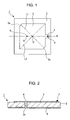
- Fig. 1 is a plan view showing a patch antenna according to a first embodiment of the present invention
- Fig. 2 is a cross sectional view of the patch antenna
- Fig. 3 is a characteristic diagram showing radiation gain of the patch antenna in an elevation angle direction.
- a patch antenna 1 shown in these drawings generally includes a dielectric substrate 2, a radiating conductor 3 and a feeding conductor 4 disposed on the top surface of the dielectric substrate 2, a ground conductor 5 disposed on the bottom surface of the dielectric substrate 2, and a short-circuit conductor 6 provided in a through hole 2a penetrating through the dielectric substrate 2.
- the radiating conductor 3 is patterned to be substantially square-shaped, and two corners corresponding to either end of one diagonal L1 of the square are cut so as to remove triangular portions and loaded with degeneracy splitting elements 3a.
- the feeding conductor 4 extends outward in the radial direction of the radiating conductor 3 to be projected from a position in the middle of an edge of the radiating conductor 3 by a certain distance, and a tip of the feeding conductor 4 functions as a feeding section F, whereby a planar-feed-type patch antenna is configured.
- the ground conductor 5 is disposed substantially over the bottom surface of the dielectric substrate 2, and the radiating conductor 3 opposes the ground conductor 5 with the dielectric substrate 2 interposed therebetween. This provides a structure of a dielectric patch antenna.
- An upper end of the short-circuit conductor 6 is connected to the radiating conductor 3 at a predetermined position thereof, and a lower end thereof is connected to the ground conductor 5.
- a short-circuit point S that is a connection location on the radiating conductor 3 connected to the short-circuit conductor 6 is electrically connected to the ground conductor 5 via the short-circuit conductor 6.
- the short-circuit point S is set on an extension of a line P connecting the center O of the radiating conductor 3 and the feeding conductor 4 (feeding section F), namely, it is set at a position deviated toward the side opposite the feeding conductor 4 by a predetermined distance from the center O of the radiating conductor 3.
- the patch antenna 1 is designed such that a length of the one diagonal L1 of the radiating conductor 3 (a distance between the pair of degeneracy splitting elements 3a and 3a) is shorter than a length of the other diagonal L2 by a certain distance, and a phase difference of about 90 degrees is generated between an excitation mode along the diagonal L1 and an excitation mode along the diagonal L2. Accordingly, the patch antenna 1 is_operated as a one-point feed type, circularly polarized antenna, by applying a feed signal at a predetermined frequency to the feeding section F.
- the radiating conductor 3 has a 0 ⁇ impedance point, at which voltage becomes zero in feeding, provided at the connection location (short-circuit point S) at which the radiating conductor 3 is connected to the short-circuit conductor 6 and the connection location is deviated from the center O of the radiating conductor 3, distributions of voltage and current of the radiating conductor 3 would be largely different from those in a case where the short-circuit conductor 6 is not provided.
- a current distribution curve of the radiating conductor 3 extending along the left-right direction shown in Fig. 2 reaches the maximum value in the vicinity of the short-circuit point S, but varies relatively gently.
- the patch antenna 1 may have the feeding section F with the impedance of 50 ⁇ in the feeding conductor 4 extending outward from the radiating conductor 3. Owing to this, feeding with achievement of impedance matching is available if a coaxial cable or the like with a characteristic impedance of 50 ⁇ is connected to the feeding section F.
- the patch antenna 1 may set the feeding section F with the impedance of 50 ⁇ in the feeding conductor 4 extending outward in the radial direction from the radiating conductor 3. Consequently, the patch antenna may be reduced in size since the impedance matching circuit is not necessary even though the slits are not formed in the radiating conductor 3.
- the radiating conductor 3 since it is not necessary to form the slits in the radiating conductor 3, the radiating conductor 3 may be easily designed to be of a shape having a good axial ratio characteristic, thereby easily securing a necessary amount of radiation gain. For example, a gain at the elevation angle of 90 degrees is as good as about 2.4 dBic.
- the short-circuit conductor 6 is only required to be provided at one location of the dielectric substrate 2 in the through hole 2a, thereby simplifying the structure, facilitating manufacturing, and promoting easy mass production.
- Fig. 4 is a plan view showing a patch antenna according to a second embodiment. Like numbers refer to like components shown in Fig. 1, and the description thereof is omitted.
- a patch antenna 10 shown in Fig. 4 is different from the one described in the first embodiment in that two short-circuit conductors are connected to the radiating conductor 3 at two locations.
- a short-circuit point S1 disposed on the one diagonal L1 of the radiating conductor 3 is connected to an upper end of a first short-circuit conductor 11, and a short-circuit point S2 disposed on the other diagonal L2 is connected to an upper end of a second short-circuit conductor 12.
- Both lower ends of the short-circuit conductors 11 and 12 are connected to the ground conductor (not shown) at the bottom surface of the dielectric substrate 2.
- the short-circuit point S1 and the short-circuit point S2 are separately provided at the two locations in the radiating conductor 3, it becomes possible to adjust the resonance characteristics appropriately for both of the two excitation modes which are electrically and spatially orthogonal to each other, thereby further enhancing improvement of the axial ratio characteristic.
Landscapes
- Waveguide Aerials (AREA)
Abstract
Description
- The present invention relates to a planar-feed-type patch antenna capable of feeding electricity to a radiating conductor in the same plane as the radiating conductor is disposed, and more particularly, it relates to a patch antenna operated as a circularly polarized antenna.
- A planar-feed-type patch antenna typically has a radiating conductor and an impedance matching circuit disposed on one surface of a dielectric substrate, and a ground conductor disposed on the other surface of the dielectric substrate in at least a region opposing the radiating conductor. A feed signal is applied to a certain position at an edge of the radiating conductor via the impedance matching circuit. However, since the impedance matching circuit is provided in the configuration, the patch antenna may be consequently of large size.
- Heretofore, there is known a patch antenna in which a pair of slits are formed at edges of the radiating conductor, and a feeding section is provided within a band-like region interposed between the slits, so that electricity may be fed directly to the feeding section (for example, see
Japanese Unexamined Patent Application Publication No. 5-259731 pages 2 to 4, Fig. 2). The above-mentioned known patch antenna is used for linear polarization, and impedance may be adjusted by properly determining the depth of the pair of slits sandwiching the feeding section. Accordingly, additional provision of the impedance matching circuit is not necessary, thereby promoting reduction in size of the patch antenna. - As described in the related art, the method of adjusting the impedance according to the formation of the slits at the edges of the radiating conductor would not cause any problem when it is applied to a linearly polarized antenna. However, when the method is applied to a circularly polarized antenna, it may be difficult to obtain a good axial ratio characteristic, inevitably causing deterioration in radiation gain. In particular, when the known method is applied to the circularly polarized antenna, it is necessary to form slits not only in the vicinity of the feeding section of the radiating conductor for the impedance adjustment, but also at other edges extending in a direction orthogonal to the former slits, for compensation. However, when the number and variety of the slits formed in the radiating conductor increase, it may be difficult to adjust resonance characteristics appropriately for both of the two excitation modes which are electrically and spatially orthogonal to each other, and accordingly, the axial ratio characteristic of the circular polarization may be deteriorated.
- In light of the above-described circumstances of the related art, an object of the present invention is to provide a planar-feed-type patch antenna for circular polarization providing a good axial ratio characteristic and being of reduced size.
- To attain the above-described object, a patch antenna according to an aspect of the present invention includes: a ground conductor; a radiating conductor which is loaded with a degeneracy splitting element and disposed so as to oppose the ground conductor with a predetermined distance therebetween; a feeding conductor which extends from the radiating conductor outward in the radial direction of the radiating conductor so that a tip of the feeding conductor functions as a feeding section; and a short-circuit conductor which is disposed to connect the radiating conductor to the ground conductor at a predetermined position in a region of the radiating conductor opposite to the feeding conductor.
- With the radiating conductor of the patch antenna configured as described above, a 0 Ω impedance point, at which voltage becomes zero in feeding, is provided at a location deviated from the center of the radiating conductor and at which the radiating conductor is connected to the short-circuit conductor, and distributions of voltage and current would be largely different from those in a case where the short-circuit conductor is not provided. Accordingly, it is possible to set the feeding section with an impedance of 50 Ω in the feeding conductor extending outward from the radiating conductor. Owing to this, feeding with achievement of impedance matching is available if a coaxial cable or the like with a characteristic impedance of 50 Ω is connected to the feeding section disposed in the feeding conductor, and the patch antenna may be of reduced size even though the slits are not formed in the radiating conductor. In addition, since it is not necessary to form the slits in the radiating conductor, it is easy to design the radiating conductor to be of a shape having a good axial ratio characteristic.
- In the above-described configuration, the number of the short-circuit conductors is appropriately determined on the basis of the location on the radiating conductor at which the short-circuit conductor is connected. For example, when the short-circuit conductor is connected to the radiating conductor at the predetermined position disposed on an extension of a line connecting the center of the radiating conductor and the feeding conductor, the short-circuit conductor is required to be provided only at this one location, thereby facilitating manufacturing. Alternatively, when a first short-circuit conductor is connected to the radiating conductor at a predetermined position on a first line connecting the center of the radiating conductor and the degeneracy splitting element, and a second short-circuit conductor is connected to the radiating conductor at a predetermined position on a second line orthogonal to the first line and passing through the center of the radiating conductor, the short-circuit conductors are provided at these two locations, and accordingly, it becomes possible to adjust the resonance characteristics appropriately for both of the two excitation modes which are electrically and spatially orthogonal to each other, thereby further enhancing improvement of the axial ratio characteristic.
- In addition, in the above-described configuration, the radiating conductor and the feeding conductor may be disposed on one surface of a dielectric substrate, whereas the ground conductor may be disposed on the other surface of the dielectric substrate, and the short-circuit conductor is provided in a through hole penetrating through the dielectric substrate. This configuration is preferable because it may provide a patch antenna having a simple structure and promoting mass production.
- With the patch antenna according to the present invention, it is possible to set the feeding section with the impedance of 50 Ω in the feeding conductor extending outward in the radial direction from the radiating conductor, by connecting the short-circuit conductor to the radiating conductor at the predetermined position deviated from the center of the radiating conductor, in the radiating conductor loaded with the degeneracy splitting element. Accordingly, there may be provided a patch antenna that is preferable for achieving reduction in size and does not need the impedance matching circuit even though the slits are not formed in the radiating conductor. In addition, since it is not necessary to form the slits in the radiating conductor, the radiating conductor may be easily designed to be of a shape having a good axial ratio characteristic, thereby facilitating manufacturing of a patch antenna for circular polarization which may secure a necessary amount of radiation gain.
-
- Fig. 1 is a plan view showing a patch antenna according to a first embodiment of the present invention;
- Fig. 2 is a cross sectional view of the patch antenna;
- Fig. 3 is a characteristic diagram showing radiation gain of the patch antenna in an elevation angle direction; and
- Fig. 4 is a plan view showing a patch antenna according to a second embodiment of the present invention.
- For describing an embodiment of the present invention with reference to the attached drawings, Fig. 1 is a plan view showing a patch antenna according to a first embodiment of the present invention, Fig. 2 is a cross sectional view of the patch antenna, and Fig. 3 is a characteristic diagram showing radiation gain of the patch antenna in an elevation angle direction.
- A patch antenna 1 shown in these drawings generally includes a
dielectric substrate 2, aradiating conductor 3 and afeeding conductor 4 disposed on the top surface of thedielectric substrate 2, aground conductor 5 disposed on the bottom surface of thedielectric substrate 2, and a short-circuit conductor 6 provided in a throughhole 2a penetrating through thedielectric substrate 2. Theradiating conductor 3 is patterned to be substantially square-shaped, and two corners corresponding to either end of one diagonal L1 of the square are cut so as to remove triangular portions and loaded withdegeneracy splitting elements 3a. Thefeeding conductor 4 extends outward in the radial direction of theradiating conductor 3 to be projected from a position in the middle of an edge of theradiating conductor 3 by a certain distance, and a tip of thefeeding conductor 4 functions as a feeding section F, whereby a planar-feed-type patch antenna is configured. Theground conductor 5 is disposed substantially over the bottom surface of thedielectric substrate 2, and theradiating conductor 3 opposes theground conductor 5 with thedielectric substrate 2 interposed therebetween. This provides a structure of a dielectric patch antenna. An upper end of the short-circuit conductor 6 is connected to theradiating conductor 3 at a predetermined position thereof, and a lower end thereof is connected to theground conductor 5. Thus, a short-circuit point S that is a connection location on theradiating conductor 3 connected to the short-circuit conductor 6 is electrically connected to theground conductor 5 via the short-circuit conductor 6. The short-circuit point S is set on an extension of a line P connecting the center O of theradiating conductor 3 and the feeding conductor 4 (feeding section F), namely, it is set at a position deviated toward the side opposite thefeeding conductor 4 by a predetermined distance from the center O of theradiating conductor 3. - The patch antenna 1 is designed such that a length of the one diagonal L1 of the radiating conductor 3 (a distance between the pair of
degeneracy splitting elements radiating conductor 3 has a 0 Ω impedance point, at which voltage becomes zero in feeding, provided at the connection location (short-circuit point S) at which theradiating conductor 3 is connected to the short-circuit conductor 6 and the connection location is deviated from the center O of theradiating conductor 3, distributions of voltage and current of theradiating conductor 3 would be largely different from those in a case where the short-circuit conductor 6 is not provided. For example, a current distribution curve of theradiating conductor 3 extending along the left-right direction shown in Fig. 2 reaches the maximum value in the vicinity of the short-circuit point S, but varies relatively gently. Thus, the patch antenna 1 may have the feeding section F with the impedance of 50 Ω in thefeeding conductor 4 extending outward from theradiating conductor 3. Owing to this, feeding with achievement of impedance matching is available if a coaxial cable or the like with a characteristic impedance of 50 Ω is connected to the feeding section F. - The patch antenna 1 according to the present embodiment may set the feeding section F with the impedance of 50 Ω in the
feeding conductor 4 extending outward in the radial direction from theradiating conductor 3. Consequently, the patch antenna may be reduced in size since the impedance matching circuit is not necessary even though the slits are not formed in theradiating conductor 3. In addition, since it is not necessary to form the slits in theradiating conductor 3, theradiating conductor 3 may be easily designed to be of a shape having a good axial ratio characteristic, thereby easily securing a necessary amount of radiation gain. For example, a gain at the elevation angle of 90 degrees is as good as about 2.4 dBic. Further, the short-circuit conductor 6 is only required to be provided at one location of thedielectric substrate 2 in the throughhole 2a, thereby simplifying the structure, facilitating manufacturing, and promoting easy mass production. - Fig. 4 is a plan view showing a patch antenna according to a second embodiment. Like numbers refer to like components shown in Fig. 1, and the description thereof is omitted.
- A
patch antenna 10 shown in Fig. 4 is different from the one described in the first embodiment in that two short-circuit conductors are connected to theradiating conductor 3 at two locations. In particular, with thepatch antenna 10, a short-circuit point S1 disposed on the one diagonal L1 of theradiating conductor 3 is connected to an upper end of a first short-circuit conductor 11, and a short-circuit point S2 disposed on the other diagonal L2 is connected to an upper end of a second short-circuit conductor 12. Both lower ends of the short-circuit conductors dielectric substrate 2. Since the short-circuit point S1 and the short-circuit point S2 are separately provided at the two locations in theradiating conductor 3, it becomes possible to adjust the resonance characteristics appropriately for both of the two excitation modes which are electrically and spatially orthogonal to each other, thereby further enhancing improvement of the axial ratio characteristic.
Claims (4)
- A patch antenna comprising:a ground conductor;a radiating conductor which is loaded with a degeneracy splitting element and disposed so as to oppose the ground conductor with a predetermined distance therebetween;a feeding conductor which extends from the radiating conductor outward in the radial direction of the radiating conductor so that a tip of the feeding conductor functions as a feeding section; anda short-circuit conductor which is disposed to connect the radiating conductor to the ground conductor at a predetermined position in a region of the radiating conductor opposite to the feeding conductor.
- The patch antenna according to Claim 1, wherein the short-circuit conductor is connected to the radiating conductor at the predetermined position disposed on an extension of a line connecting the center of the radiating conductor and the feeding conductor.
- The patch antenna according to Claim 1, wherein a first short-circuit conductor is connected to the radiating conductor at a predetermined position on a first line connecting the center of the radiating conductor and the degeneracy splitting element, and a second short-circuit conductor is connected to the radiating conductor at a predetermined position on a second line orthogonal to the first line and passing through the center of the radiating conductor.
- The patch antenna according to any one of Claims 1 through 3, wherein the radiating conductor and the feeding conductor are disposed on one surface of a dielectric substrate, whereas the ground conductor is disposed on the other surface of the dielectric substrate, and the short-circuit conductor is provided in a through hole penetrating through the dielectric substrate.
Applications Claiming Priority (1)
| Application Number | Priority Date | Filing Date | Title |
|---|---|---|---|
| JP2005355070A JP2007159031A (en) | 2005-12-08 | 2005-12-08 | Patch antenna |
Publications (2)
| Publication Number | Publication Date |
|---|---|
| EP1796212A1 true EP1796212A1 (en) | 2007-06-13 |
| EP1796212B1 EP1796212B1 (en) | 2009-07-22 |
Family
ID=37763924
Family Applications (1)
| Application Number | Title | Priority Date | Filing Date |
|---|---|---|---|
| EP20060025245 Expired - Fee Related EP1796212B1 (en) | 2005-12-08 | 2006-12-06 | Patch antenna |
Country Status (4)
| Country | Link |
|---|---|
| EP (1) | EP1796212B1 (en) |
| JP (1) | JP2007159031A (en) |
| DE (1) | DE602006007936D1 (en) |
| SG (1) | SG133500A1 (en) |
Cited By (5)
| Publication number | Priority date | Publication date | Assignee | Title |
|---|---|---|---|---|
| CN104868239A (en) * | 2015-04-22 | 2015-08-26 | 哈尔滨工业大学 | Single-feed circular slit loading broadband circular polarization microstrip antenna |
| WO2018011635A1 (en) * | 2016-07-14 | 2018-01-18 | Alcatel Lucent | Microstrip antenna, antenna array and method of manufacturing microstrip antenna |
| CN111916905A (en) * | 2020-07-27 | 2020-11-10 | 华南理工大学 | Wearable dual-frequency dual-polarized antenna and wearable terminal equipment |
| CN113711441A (en) * | 2019-04-26 | 2021-11-26 | 日本电业工作株式会社 | Antenna device |
| CN119253262A (en) * | 2024-11-20 | 2025-01-03 | 安徽雷图科技有限公司 | A Ku-band microstrip phased array antenna unit |
Families Citing this family (1)
| Publication number | Priority date | Publication date | Assignee | Title |
|---|---|---|---|---|
| US20180175493A1 (en) * | 2016-12-15 | 2018-06-21 | Nanning Fugui Precision Industrial Co., Ltd. | Antenna device and electronic device using the same |
Citations (5)
| Publication number | Priority date | Publication date | Assignee | Title |
|---|---|---|---|---|
| US4095227A (en) | 1976-11-10 | 1978-06-13 | The United States Of America As Represented By The Secretary Of The Navy | Asymmetrically fed magnetic microstrip dipole antenna |
| FR2552937A1 (en) * | 1983-10-04 | 1985-04-05 | Dassault Electronique | RADIANT DEVICE WITH MICROBAND STRUCTURE WITH INTERFERENCE ELEMENT |
| WO2001031739A1 (en) * | 1999-10-08 | 2001-05-03 | Antennas America, Inc. | Compact microstrip antenna for gps applications |
| EP1241733A1 (en) | 2001-03-15 | 2002-09-18 | Alcatel | PIFA antenna with slots |
| US20040196200A1 (en) * | 2003-04-04 | 2004-10-07 | Sievenpiper Daniel F. | Low-profile antenna |
Family Cites Families (7)
| Publication number | Priority date | Publication date | Assignee | Title |
|---|---|---|---|---|
| US6140965A (en) * | 1998-05-06 | 2000-10-31 | Northrop Grumman Corporation | Broad band patch antenna |
| US5969681A (en) * | 1998-06-05 | 1999-10-19 | Ericsson Inc. | Extended bandwidth dual-band patch antenna systems and associated methods of broadband operation |
| US6346913B1 (en) * | 2000-02-29 | 2002-02-12 | Lucent Technologies Inc. | Patch antenna with embedded impedance transformer and methods for making same |
| JP2003243926A (en) * | 2002-02-15 | 2003-08-29 | Alps Electric Co Ltd | Patch antenna |
| JP2004165980A (en) * | 2002-11-13 | 2004-06-10 | Alps Electric Co Ltd | Patch antenna |
| US6977613B2 (en) * | 2003-12-30 | 2005-12-20 | Hon Hai Precision Ind. Co., Ltd. | High performance dual-patch antenna with fast impedance matching holes |
| JP3983224B2 (en) * | 2004-01-16 | 2007-09-26 | アルプス電気株式会社 | Patch antenna |
-
2005
- 2005-12-08 JP JP2005355070A patent/JP2007159031A/en not_active Withdrawn
-
2006
- 2006-11-29 SG SG200608346-3A patent/SG133500A1/en unknown
- 2006-12-06 EP EP20060025245 patent/EP1796212B1/en not_active Expired - Fee Related
- 2006-12-06 DE DE200660007936 patent/DE602006007936D1/en active Active
Patent Citations (5)
| Publication number | Priority date | Publication date | Assignee | Title |
|---|---|---|---|---|
| US4095227A (en) | 1976-11-10 | 1978-06-13 | The United States Of America As Represented By The Secretary Of The Navy | Asymmetrically fed magnetic microstrip dipole antenna |
| FR2552937A1 (en) * | 1983-10-04 | 1985-04-05 | Dassault Electronique | RADIANT DEVICE WITH MICROBAND STRUCTURE WITH INTERFERENCE ELEMENT |
| WO2001031739A1 (en) * | 1999-10-08 | 2001-05-03 | Antennas America, Inc. | Compact microstrip antenna for gps applications |
| EP1241733A1 (en) | 2001-03-15 | 2002-09-18 | Alcatel | PIFA antenna with slots |
| US20040196200A1 (en) * | 2003-04-04 | 2004-10-07 | Sievenpiper Daniel F. | Low-profile antenna |
Non-Patent Citations (2)
| Title |
|---|
| WEN-SHYANG CHEN: "Inset-microstripline-fed circularly polarized microstrip antennas", ANTENNAS AND PROPAGATION SOCIETY, 1999. IEEE INTERNATIONAL SYMPOSIUM 1999 ORLANDO, FL, USA 11-16 JULY 1999, PISCATAWAY, NJ, USA,IEEE, US, vol. 1, 11 July 1999 (1999-07-11), pages 260 - 263, XP010348247, ISBN: 0-7803-5639-X * |
| WEN-SHYANG CHEN: "Inset-microstripline-fed circularly polarized microstrip antennas", ANTENNAS AND PROPAGATION SOCIETY, vol. 1, 11 July 1999 (1999-07-11), pages 260 - 263 |
Cited By (7)
| Publication number | Priority date | Publication date | Assignee | Title |
|---|---|---|---|---|
| CN104868239A (en) * | 2015-04-22 | 2015-08-26 | 哈尔滨工业大学 | Single-feed circular slit loading broadband circular polarization microstrip antenna |
| WO2018011635A1 (en) * | 2016-07-14 | 2018-01-18 | Alcatel Lucent | Microstrip antenna, antenna array and method of manufacturing microstrip antenna |
| CN107623187A (en) * | 2016-07-14 | 2018-01-23 | 上海诺基亚贝尔股份有限公司 | Microstrip antenna, aerial array and microstrip antenna manufacture method |
| CN113711441A (en) * | 2019-04-26 | 2021-11-26 | 日本电业工作株式会社 | Antenna device |
| CN111916905A (en) * | 2020-07-27 | 2020-11-10 | 华南理工大学 | Wearable dual-frequency dual-polarized antenna and wearable terminal equipment |
| CN111916905B (en) * | 2020-07-27 | 2025-05-13 | 华南理工大学 | A wearable dual-frequency dual-polarization antenna and a wearable terminal device |
| CN119253262A (en) * | 2024-11-20 | 2025-01-03 | 安徽雷图科技有限公司 | A Ku-band microstrip phased array antenna unit |
Also Published As
| Publication number | Publication date |
|---|---|
| SG133500A1 (en) | 2007-07-30 |
| JP2007159031A (en) | 2007-06-21 |
| DE602006007936D1 (en) | 2009-09-03 |
| EP1796212B1 (en) | 2009-07-22 |
Similar Documents
| Publication | Publication Date | Title |
|---|---|---|
| US6326923B2 (en) | Small-sized circular polarized wave microstrip antenna providing desired resonance frequency and desired axis ratio | |
| US7075486B2 (en) | Circularly polarized wave antenna made of sheet metal with high reliability | |
| US4843400A (en) | Aperture coupled circular polarization antenna | |
| US20050116875A1 (en) | Antenna device suitable for miniaturization | |
| US8098203B2 (en) | Antenna and communication device having the same | |
| JP2005079970A (en) | Antenna system | |
| CN1722518A (en) | Differentially fed multilayer antenna | |
| JP6658439B2 (en) | Antenna device | |
| EP1513223A1 (en) | Dual-band antenna with adjustable resonant frequency, and method for adjusting resonant frequency | |
| EP3518344A1 (en) | Antenna device | |
| KR20200035161A (en) | Array antenna device | |
| US20130120198A1 (en) | Antenna device | |
| EP1796212B1 (en) | Patch antenna | |
| JP4418375B2 (en) | Antenna device | |
| US6437744B1 (en) | Circularly polarized wave antenna device | |
| JP4103936B2 (en) | Antenna structure and wireless communication device including the same | |
| JP2026065121A (en) | Antenna equipment | |
| US20230145638A1 (en) | Antenna device | |
| JP4265654B2 (en) | Circularly polarized microstrip antenna and wireless communication device including the same | |
| JPH07307613A (en) | Circular polarized wave microstrip antenna | |
| KR20100041608A (en) | Circular polarization dielectric resonator antenna | |
| JP4336259B2 (en) | Circularly polarized microstrip antenna and multifrequency antenna | |
| JP2007208692A (en) | Patch antenna | |
| JP6314722B2 (en) | Circularly polarized patch antenna and integrated antenna device | |
| JPS61218206A (en) | Dipole connection type folded antenna |
Legal Events
| Date | Code | Title | Description |
|---|---|---|---|
| PUAI | Public reference made under article 153(3) epc to a published international application that has entered the european phase |
Free format text: ORIGINAL CODE: 0009012 |
|
| AK | Designated contracting states |
Kind code of ref document: A1 Designated state(s): AT BE BG CH CY CZ DE DK EE ES FI FR GB GR HU IE IS IT LI LT LU LV MC NL PL PT RO SE SI SK TR |
|
| AX | Request for extension of the european patent |
Extension state: AL BA HR MK YU |
|
| 17P | Request for examination filed |
Effective date: 20070822 |
|
| AKX | Designation fees paid |
Designated state(s): DE FR GB |
|
| 17Q | First examination report despatched |
Effective date: 20080724 |
|
| GRAP | Despatch of communication of intention to grant a patent |
Free format text: ORIGINAL CODE: EPIDOSNIGR1 |
|
| GRAS | Grant fee paid |
Free format text: ORIGINAL CODE: EPIDOSNIGR3 |
|
| GRAA | (expected) grant |
Free format text: ORIGINAL CODE: 0009210 |
|
| AK | Designated contracting states |
Kind code of ref document: B1 Designated state(s): DE FR GB |
|
| REG | Reference to a national code |
Ref country code: GB Ref legal event code: FG4D |
|
| REF | Corresponds to: |
Ref document number: 602006007936 Country of ref document: DE Date of ref document: 20090903 Kind code of ref document: P |
|
| PGFP | Annual fee paid to national office [announced via postgrant information from national office to epo] |
Ref country code: FR Payment date: 20091120 Year of fee payment: 4 |
|
| PLBE | No opposition filed within time limit |
Free format text: ORIGINAL CODE: 0009261 |
|
| STAA | Information on the status of an ep patent application or granted ep patent |
Free format text: STATUS: NO OPPOSITION FILED WITHIN TIME LIMIT |
|
| 26N | No opposition filed |
Effective date: 20100423 |
|
| PGFP | Annual fee paid to national office [announced via postgrant information from national office to epo] |
Ref country code: DE Payment date: 20091130 Year of fee payment: 4 |
|
| GBPC | Gb: european patent ceased through non-payment of renewal fee |
Effective date: 20101206 |
|
| REG | Reference to a national code |
Ref country code: FR Ref legal event code: ST Effective date: 20110831 |
|
| PG25 | Lapsed in a contracting state [announced via postgrant information from national office to epo] |
Ref country code: FR Free format text: LAPSE BECAUSE OF NON-PAYMENT OF DUE FEES Effective date: 20110103 |
|
| PG25 | Lapsed in a contracting state [announced via postgrant information from national office to epo] |
Ref country code: GB Free format text: LAPSE BECAUSE OF NON-PAYMENT OF DUE FEES Effective date: 20101206 Ref country code: DE Free format text: LAPSE BECAUSE OF NON-PAYMENT OF DUE FEES Effective date: 20110701 |
|
| REG | Reference to a national code |
Ref country code: DE Ref legal event code: R119 Ref document number: 602006007936 Country of ref document: DE Effective date: 20110701 |