EP1793412A1 - Filament lamp - Google Patents
Filament lamp Download PDFInfo
- Publication number
- EP1793412A1 EP1793412A1 EP06024647A EP06024647A EP1793412A1 EP 1793412 A1 EP1793412 A1 EP 1793412A1 EP 06024647 A EP06024647 A EP 06024647A EP 06024647 A EP06024647 A EP 06024647A EP 1793412 A1 EP1793412 A1 EP 1793412A1
- Authority
- EP
- European Patent Office
- Prior art keywords
- filament
- lamp
- insulator
- bulb
- treated
- Prior art date
- Legal status (The legal status is an assumption and is not a legal conclusion. Google has not performed a legal analysis and makes no representation as to the accuracy of the status listed.)
- Granted
Links
Images



Classifications
-
- H—ELECTRICITY
- H01—ELECTRIC ELEMENTS
- H01K—ELECTRIC INCANDESCENT LAMPS
- H01K5/00—Lamps for general lighting
- H01K5/02—Lamps for general lighting with connections made at opposite ends, e.g. tubular lamp with axially arranged filament
-
- H—ELECTRICITY
- H01—ELECTRIC ELEMENTS
- H01K—ELECTRIC INCANDESCENT LAMPS
- H01K1/00—Details
- H01K1/38—Seals for leading-in conductors
-
- H—ELECTRICITY
- H01—ELECTRIC ELEMENTS
- H01J—ELECTRIC DISCHARGE TUBES OR DISCHARGE LAMPS
- H01J5/00—Details relating to vessels or to leading-in conductors common to two or more basic types of discharge tubes or lamps
- H01J5/32—Seals for leading-in conductors
Definitions
- the invention relates to a filament lamp.
- the invention relates especially to a filament lamp for irradiation of an article to be treated with light which is emitted for purposes of heating of the article to be treated.
- heat treatment is used in different processes, such as a layer formation, oxidation-diffusion, diffusion of impurities, nitriding, layer stabilization, silicide formation, crystallization, ion implantation activation and the like.
- RTP rapid thermal processing
- the temperature of the article to be treated such as a semiconductor wafer or the like
- a heat treatment device of the light irradiation type (hereinafter also called only a heating device) using light irradiation from a light source, such as a filament lamp or the like, is widely used.
- a filament lamp in which there is a filament within a bulb of transparent material is a typical lamp in which light can be used to produce heat since, in this connection, at least 90 % of the input power is converted to heat and since heating is possible without contact with the article to be treated.
- the temperature of the article to be treated can be raised/lowered more quickly than in a resistance heating process.
- the temperature of the article to be treated can be raised to at least 1000 °C in from ten to a few dozen seconds. After light irradiation has been stopped, the article to be treated is rapidly cooled. This heat treatment of the light irradiation type is normally done several times.
- the article to be treated is, for example, a semiconductor wafer (silicon wafer)
- a nonuniformity occurs as the semiconductor wafer is heated to at least 1050 °C
- a phenomenon called slip occurs in the semiconductor wafer, i.e., a defect of crystal transition, by which the danger arises that scrap will be formed.
- RTP of a semiconductor wafer is carried out using a heat treatment device of the light irradiation type, heating must be performed, a high temperature maintained and then cooling must produced such that the temperature distribution of the overall surface of the semiconductor wafer becomes uniform. This means that, in RTP, there is a need for very precise temperature uniformity of the article to be treated.
- the temperature of the semiconductor wafer does not become uniform even if light irradiation is performed such that the irradiance becomes uniform on the entire surface of the semiconductor wafer.
- the temperature of the peripheral region of the semiconductor wafer is low. This is because in the peripheral region of the semiconductor wafer heat is radiated from the semiconductor wafer side. As a result of this heat release, a temperature distribution forms in the semiconductor wafer.
- a semiconductor wafer slip occurs when a nonuniformity in the temperature distribution of the semiconductor wafer arises in the heating of the semiconductor wafer to at least 1050 °C.
- Patent document 1 JP HEI 7-37833 A discloses a conventional heating device in which light emitted by a filament lamp is used to heat a glass substrate and a semiconductor wafer.
- This heating device has the arrangement shown in Figure 6 in which in a chamber of transparent material there is the article to be treated and on a top step and a bottom step, therefore on two steps outside of this chamber there are several opposed filament lamps at top and bottom, and moreover, crossing one another, and in which the article to be treated is irradiated with light from both sides and heated.
- Figure 7 is a perspective in which the above described device is shown simplified and the filament lamps located on the top step and bottom step, therefore on the two steps, for heating and the article to be treated are shown.
- the filament lamps for heating which are located on the top step and the bottom step, therefore on the two steps are arranged such that the bulb axes cross.
- the article to be treated can therefore be heated uniformly.
- this device can prevent a temperature drop by the action of heat radiation in the peripheral area of the article to be treated.
- the lamp output of the filament lamps for heating L1, L2 located on the two sides of the top step is made larger than the lamp output of a lamp L3 for heating located in the middle area.
- the lamp output of the filament lamps for heating L4, L5 located on the two sides of the bottom step is made larger than the lamp output of a lamp L6 for heating located in the middle area. In this way, the amount of temperature drop by the action of heat radiation in the peripheral area of the article to be treated can be equalized, the temperature difference between the middle area and the peripheral area of the article to be treated can be reduced and the temperature distribution of the article to be treated can be made uniform.
- the article to be treated is a semiconductor wafer
- a film of a metal oxide or the like is formed on the surface of the semiconductor by a sputtering process or the like, or foreign ion material is doped by ion implantation.
- the layer thickness of this metal oxide or the density of the foreign ions on the wafer surface has a local distribution which is not always centrosymmetric to the middle of the semiconductor wafer.
- the density of foreign ions there is a case according to Figure 7 in which the density of foreign ions changes in a narrow, special region which is not centrosymmetric to the middle of the semiconductor wafer.
- the above described conventional heating device makes it possible to relatively easily equalize the effect of the temperature drop by heat radiation in the peripheral area of the region to be treated, to prevent a temperature drop in the peripheral area and to make the temperature distribution of the article to be treated uniform in a certain narrow region with a total length which is less than the emission length of the lamp, however, as is shown, for example, in Figure 7, a region outside of the above described certain region is also irradiated with light, even if light irradiation is performed with an intensity which corresponds to the property of this certain region. Therefore, control cannot be exercised in such a manner that the above described certain region and the other region are shifted into suitable temperature state.
- a heat treatment device in which there are a first lamp unit and a second lamp unit in the lamp housing.
- first lamp unit several U-shaped double-end lamps in which there are feed devices for the filaments on the two ends of the bulb are arranged perpendicular and parallel to the page of the drawing.
- second lamp unit several straight, double-end lamps which are located under the first lamp unit and in which on the two ends of the bulb there are feed devices for the filaments are located along the page of the drawings in the direction perpendicular to the page of the drawing.
- an article such as a semiconductor wafer or the like, which is located underneath the second lamp unit, is heat treated.
- this heat treatment device yields a device which exercises control such that the U-shaped lamps of the first lamp unit which are located above the connecting part have a high output in order to increase the temperature of the connecting part on a support ring on which the article to be treated is placed, this connecting part having a tendency to have a lower temperature than the remaining region.
- the heating area of the semiconductor wafer as the article to be treated is divided into several zones which are centrosymmetric and concentric.
- artificial illuminance distribution patterns are formed which correspond to the respective zone and which are centrosymmetric to the middle of the semiconductor.
- heating is carried out according to the temperature change of the respective zone.
- the semiconductor wafer which constitutes the article to be treated is rotated to suppress the effect of the scattering of the illuminance of the lamp radiation. This means that the respective concentrically arranged zone can be heat treated at an individual illuminance.
- a U-shaped lamp is formed of a horizontal region and a pair of vertical regions.
- the individual lamps are apart from one another over a space which cannot be ignored. Therefore, it can be imagined that a temperature distribution forms in the region which is located directly underneath this space.
- FIG. 9 is a schematic perspective view of the basic arrangement of a filament lamp as disclosed in commonly-owned, co-pending U.S. Patent Application 11/362,788 (Patent Application Publication 2006/0197454 A1) relative to which one of the inventors of the present invention is a co-inventor and constitutes a precursor to the present invention.
- This filament lamp has several filaments in a bulb and separate control of emission and the like of the each filament is possible.
- a heat treatment device of the light irradiation type with light source parts in which these filament lamps are arranged parallel to one another compared to the case of using a conventional filament lamp with a single filament in the bulb several filaments can be supplied individually.
- each filament body is arranged such that, in an arrangement of several filament bodies in the bulb, the filaments are arranged in rows in the lengthwise direction of the bulb.
- an insulator for example, of silica glass between the filaments which are arranged in rows in the lengthwise direction of the bulb.
- a lead which borders one end of a filament in one of the filament bodies passes through a through opening in the insulator.
- the outside of the point which is opposite the filament of the other filament body is covered with an insulating tube and is electrically connected to a metal foil which has been inserted in the hermetically sealed portion on one side of the end of the bulb.
- the lead which borders the other end of the filament in one of the filament bodies is electrically connected to a metal foil which is inserted in the hermetically sealed portion on the side of the other end of the bulb.
- one lead which borders one end of a filament in the other filament body passes through the through opening in the insulator.
- the outside of the point which is opposite the filament of the one filament body is covered with an insulating tube and is electrically connected to a metal foil which is inserted in the hermetically sealed portion on one side of the end of the bulb.
- the lead which borders the other end of the filament in the other filament body is electrically connected to a metal foil which has been inserted in the hermetically sealed portion on the side of the one end of the bulb.
- An outer lead is connected to the end of the metal foil which is inserted in the hermetically sealed portion which is opposite the end to which the filament body is connected, such that the outer lead projects to the outside from the hermetically sealed portion.
- Two outer leads are therefore connected via the metal foil to the respective filament body.
- a feed device is connected to each filament via the outer leads. In this way, in the filament lamp, each filament of the respective filament body can be supplied individually.
- the filament lamp shown in Figure 9 had the following disadvantages.
- the two ends of the filament lamp are hermetically terminated by a pinch seal.
- the pinch seal takes place, for example, by the outer leads being attached to the metal foils after welding of the outer leads and the leads of the filament body, the end of the bulb on which the metal foils are located being burned with a torch, and the metal foils being clamped from both sides by the metal shape which was produced in the form of the desired sealing area.
- the inventors conducted numerous studies to devise a filament lamp which has high reliability by its having a sealing arrangement in which these disadvantages, such as poor sealing and the like, do not occur, and thus they have completed the invention, as is described below.
- a primary object of the invention is to devise a filament lamp in which the article to be treated can be uniformly heated and in which, moreover, it can be used for a heat treatment device of the light irradiation type which can be made smaller, even if the distribution of the degree of the local temperature change on the substrate-like article to be heat-treated is asymmetrical to the substrate shape, or also in the case in which the degree of the local temperature change differs in certain regions.
- the inventors have invented a filament lamp with a completely different arrangement than a conventional arrangement and a heat treatment device of the light irradiation type using this filament lamp.
- This heat treatment device of the light irradiation type makes it possible to overcome the above described disadvantages of the conventional heat treatment device of the light irradiation type.
- a primary object of the invention lies especially in devising a filament lamp which acquires high reliability in that the disadvantage of poor sealing or the like does not arise for a filament lamp used for the above described heat treatment device of the light irradiation type even in the case of inserting a host of metal foils into a hermetically sealed portion.
- a filament lamp in which within the bulb several filament bodies, in which one filament and leads for supply of power to this filament are connected to one another, and in which on at least one end of the bulb there is a hermetically sealed portion in which there are several electrically conductive components which are each electrically connected to the several filament bodies, in that there is a rod-shaped insulator in the hermetically sealed portion for sealing, that moreover the several electrically conductive components are arranged spaced relative to one another in the outside periphery of the insulator for sealing, and that the bulb and the insulator are sealed at the hermetically sealed portion for sealing via the electrically conductive components.
- the object is furthermore achieved in accordance with the invention in the above described filament lamp in that the above described electrically conductive components have at least metal foils which are electrically connected to the filament bodies, and have outer leads which are electrically connected to these metal foils, and that in the insulator for sealing, positioning openings for the above described outer leads are formed.
- the "positioning openings" comprise openings and depressions which have a bottom.
- the object is furthermore achieved in accordance with the invention in that a tapering area is formed on the end at least on one side of the respective filament body of the insulator for sealing.
- the object is furthermore achieved in accordance with the invention in that the bulb has two opposite ends, each having a hermetically sealed portion and a rod-shaped sealing insulator located therein, with the several electrically conductive components being arranged spaced relative to one another in the outside peripheries of each of the insulators.
- the filament lamp in accordance with the invention within the bulb, several filament bodies in which one filament and leads for supplying power to this filament are connected to one another, and on at least one end of the bulb there is a hermetically sealed portion in which several electrically conductive components are located, which are each electrically connected to one of the several filament bodies, in the hermetically sealed portion a rod-shaped insulator for sealing is located, moreover the several electrically conductive components are located in the outer periphery of the insulator at a distance from one another, and the bulb and the insulator for sealing are hermetically sealed via the electrically conductive components between the two.
- This arrangement enables a host of metal foils to be arranged on the same periphery at distances to one another.
- the size of the hermetically sealed portion can be reduced, by which the disadvantage of poor sealing or the like never occurs and by which a filament lamp with high reliability can be devised.
- the positions of the outer leads can be positioned at defined positions.
- the thickness of the silica glass comprising the bulb and insulator for sealing can be increased. In this way the reliability of sealing can be increased.
- the lamp units as light source parts are arranged by a parallel arrangement of several filament lamps which were described above, by which setting of the intensity distribution of the light emitted from the light source parts of the filament lamps can also be controlled in the axial direction of the bulb, while setting the intensity distribution of the light emitted from the light source part of the conventional filament lamp with a single filament in the bulb could only be controlled in the direction perpendicular to the axial direction of the bulb.
- filament lamps are used in which the distance between the respective filaments to be arranged in the bulb can be reduced to an extreme degree, the effect of the distance between the filaments which is a not an emitting space can be reduced to a minimum, by which it becomes possible to make unwanted scattering of the distribution of the illuminance on the article to be treated extremely small. Since, in the vertical direction of the heating device, there is no vertical part of the lamp, the space corresponding to this within the lamp unit is no longer required, by which the heating device can be made smaller.
- Figures 1(a) is a schematic perspective view of one embodiment of a filament lamp in accordance with the invention & Fig. 1(b) is a sectional view taken along line A-A' in Fig. 1(a);
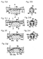
- Figures 2(a) to 2(g) each show an enlarged cross section of the vicinity of the insulator for sealing in accordance with the invention, Figs. 2(a), (c), (f), & (g) being partial longitudinal sections and Figs. 2(b), (d) and (e) being transverse sectional views;
- Figure 3 is a view similar to that of Fig. 1(a), but showing another embodiment of a filament lamp in accordance with the invention
- Figure 4 is a schematic sectional view of the arrangement of one example of a heating device into which filament lamps in accordance with the invention are installed;
- Figure 5 is a top view of the arrangement of one example of the respective filament lamp in the first lamp unit and the second lamp unit as shown in Figure 4;
- Figure 6 is a sectional view of a conventional heating device
- FIG 7 is a perspective view in which the heating device shown in Figure 6 is shown simplified, and in which heating filament lamps which are located on the top step and bottom step, and the article to be treated are shown;
- Figure 8 is a schematic cross-sectional view of a conventional heating device in a front view
- Figure 9 is a schematic perspective view of a commonly-owned precursor to the filament lamp of the present invention.
- Figures 1(a) & 1(b) show an embodiment of a filament lamp in accordance with the invention which is comprised of bulb 11 made of a transparent material such as, for example, silica glass or the like.
- the bulb has an oblong cross-sectional shape, but a circular shape can also be used.
- the term "oblong” is to be understood as encompassing all shapes in which the length a in the lengthwise direction is greater than the length b in the direction perpendicular to the lengthwise direction the cross-sectional shape, as is shown in Figure 1(b).
- the bulb 11 is filled with a halogen gas, and furthermore, there are three filament bodies 13a, 13b, and 13c in it.
- rod-shaped insulators 12a, 12b for sealing On the inside in the vicinity of the two ends.
- Electrically conductive components 150a, 150b, 150c are each electrically connected to the filament bodies 13a, 13b, 13c to at one end of the lamp, while electrically conductive components 150d, 150e, 150f are electrically connected to at the other end.
- the electrically conductive component 150a is formed of an inner lead 15a which is electrically connected to a lead 132b described below, of a metal foil 18a which is electrically connected to the inner lead 15a, and of an outer lead 17a which is electrically connected to the metal foil 18a.
- the other electrically conductive components 150b &150f, like 150a, each are comprised of an inner lead, a metal foil and an outer lead.
- the lead 132b can be directly connected to the metal foil 18a without using the inner lead. That is, the above described electrically conductive component 150a can also be comprised of a metal foil 18a which is electrically connected to the lead 132b and of an outer lead 17a which is electrically connected to the metal foil 18a. The same as for 150a, also applies to the other electrically conductive components 150b, 150f.
- the electrically conductive components of the filament lamp in accordance with the invention have both the function of supply of the filament bodies by presence between the two, i.e., the filament bodies and the feed device described below, and by the electrical leads to the two, as well as the function of the hermetic sealing described below by presence between the two, i.e., the bulbs and the insulators for sealing.
- the bulb and the insulators for sealing are hermetically sealed to one another via the metal foils.
- the electrically conductive components need not always be formed of inner leads, metal foils and outer leads, i.e., of three parts, but, for example, an electrically conductive component can be used in which the inner lead, as was described above, is omitted, and in which the lead of a filament body described below and the metal foil are electrically connected to one another. Furthermore, an arrangement can be undertaken in which a rod-shaped body or a metal foil which is routed out of the bulb is connected to the respective filament body, and in which part of this rod-shaped body or the metal foil is sealed.
- the metal foils 18a, 18b, 18c are arranged parallel to one another essentially at the same distance on the peripheral surface along the lengthwise direction of the insulator 12a.
- the metal foil 18a is connected to the inner lead 15a and the outer lead 17a.
- the metal foil 18b is connected to the inner lead 15b and the outer lead 17b.
- the metal foil 8c is connected to the inner lead 15c and the outer lead 17c.
- the metal foils 18d, 18e, 18f are arranged parallel to one another essentially with the same distance on the peripheral surface along the lengthwise direction of the insulator 12b.
- the metal foil 18d is connected to the inner lead 15d and the outer lead 17d.
- the metal foil 18e is connected to the inner lead 15e and the outer lead 17e.
- the metal foil 18f is connected to the inner lead 15f and the outer lead 17f.
- the filament body 13a is formed of a filament 131a, a lead 132a which is connected to one end of the filament 131a, and a lead 133a which is connected to the other end of the filament 131a.
- the filament body 13b is formed of a filament 131b, a lead 132b and a lead 133b.
- the filament body 13c is formed of a filament 131c, a lead 132c and a lead 133c.
- the filaments 131a, 131b and 131c are preferably coaxially arranged, but they need not be coaxially arranged; however, in the case in which the positional deviation of the filaments from one another can be equalized by simultaneous use of optical elements, such as a reflector and the like, when the distance between the article to be treated and the lamp is relatively large, when the position deviation of the filaments from one another compared to the distance between the article to be treated and the lamp is relatively small, and therefore the distribution of the illuminance is not affected, or in similar cases.
- the filaments 131 a, 131 b and 131 c are supported without contact with the bulb 11 by a spiral anchor 19 which is clamped between the inside wall of the bulb 11 and the insulating tube 18.
- the anchor 19 is used to prevent this problem from occurring.
- the anchor also has a certain elasticity so that in the production of the filament lamp several filament bodies are easily inserted into the bulb.
- separating boards 14a, 14b, 14c, 14d made of silica glass.
- the insulators 14a, 14b, 14c, 14d are used to prevent contacts with the filament bodies 13a, 13b 13c and each have three through openings.
- the lead 132a for the filament body 13a is inserted into a through opening 141a in the separating board 14a and is connected to the inner lead 15c in the insulator 12a.
- the lead 133a in the filament body 13a is inserted into the through opening 141b in the separating board 14b, an insulating tube 16b which is located opposite the filament 131b is inserted into a through opening 142c located in the separating board 14c, an insulating tube 16c which is located opposite the filament 131c is inserted into a through opening 142d located in the separating board 14d and is connected to the inner lead 15d located in the insulator 12b.
- the lead 132b in the filament body 13b is inserted into the through opening 142b located in the separating board 14b, into an insulating tube 16a which is located opposite the filament 131a, and into a through opening 142a which is located in the separating board 14a, and is connected to the inner lead 15a located in the insulator 12a.
- the lead 133b in the filament body 13b is inserted into the through opening 141 c located in the separating board 14c, into an insulating tube 16f which is located opposite the filament 131c, and into a through opening 143d located in the separating board 14d, and is connected to the inner lead 15e located in the insulator 12b.
- the lead 132c in the filament body 13c is inserted into the through opening 143c located in the separating board 14c, into the insulating tube 16e which is located opposite the filament 131b, into a through opening 143b which is located in the separating board 14b, into an insulating tube 16d which is located opposite the filament 131a, and into a through opening 143a located in the separating board 14a, and is connected to the inner lead 15b located in the insulator 12a.
- the lead 133c for the filament body 13c is inserted into the through opening 141d located in the separating board 14d and is connected to the inner lead 151 located in the insulator 12b.
- Figures 2(a) to 2(g) are each an enlarged cross-sectional view of the vicinity of the insulator 12a.
- Figure 2(a) is an enlarged cross section of important parts of a filament lamp in the lengthwise direction in order to show a first example of the sealing arrangement.
- Figure 2(b) is a transverse cross section through a section along the line B-B' of Figure 2(a).
- Figures 2(c) & Figure 2(e) each schematically show a second example of the sealing arrangement.
- Figure 2(c) is an enlarged cross section of important parts of a filament lamp in the lengthwise direction.
- Figures 2(d) & 2(e) are transverse cross sections taken alone the line C-C' and line D-D', respectively, in Figure 2(c).
- Figures 2(f) & 2(g) are enlarged cross sections of important parts of the filament lamp in the lengthwise direction showing third and fourth examples of the sealing arrangement.
- the insulator for sealing is formed of an insulating material, such as, for example, silica glass or the like.
- a metal foil 18a that extends essentially parallel along the lengthwise direction of the insulator 12a.
- the metal foil 18a is connected to the inner lead 15a and to the outer lead 17a and has a smaller total length than the insulator 12a.
- the inner lead 15a, the outer lead 17a and the metal foil 18a can be completely sealed without the metal foil 18a being exposed to the outside world.
- the inner lead 15b, the metal foil 18b, the outer lead 17b, the inner lead 15c, the metal foil 18c, and the outer lead 17c as shown in Figure 1(a) are arranged in the same way as the inner lead 15a, the metal foil 18a and the outer lead 17a.
- the inner lead 15b, the metal foil 18b, the outer lead 17b, the inner lead 15c, the metal foil 18c and the outer lead 17c have the same shapes and the same total lengths as the inner lead 15a, the metal foil 18a, and the outer lead 17a.
- the insulator 12b has the same arrangement as the insulator 12a.
- the bulb 11 and the insulator 12a are hermetically sealed via the metal foils 18a, 18b, 18c by heating the outer periphery of the bulb 11 which corresponds to the location at which the insulator 12a is located with a torch or the like, as is shown in Figure 2(b).
- the outside diameter of the insulator 12a is smaller than the inside diameter of the bulb 11.
- the bulb 11 is therefore reduced in diameter in the region which is present tightly directly adjoining the insulator 12a, specifically in the hermetically sealed portion.
- the inner lead 15c and the outer lead 17c are electrically connected to the two ends of the metal foil 18c.
- the total length of the metal foils 18a, 18b, 18c is less than the insulator 12a.
- the insulator 12b has the same arrangement as the insulator 12a.
- the depressions 121a, 121 b, 121c determine the positions of the inner leads 15a, 15b, 15c
- the depressions 122a, 122b, 122c determine the positions of the outer leads 17a, 17b, 17c.
- the depressions (in the insulator 12a) 121a, 121b, 121c for the arrangement of the inner leads 15a, 15b, 15c can also be omitted.
- the depressions for the arrangement of the inner leads 15d, 15e, 15f can also be omitted.
- an insulator 12a is used, with two ends provided with tapering regions 123a and 124a.
- the inner lead 15a and the outer lead 17a have shapes which are bent according to the shape of the tapering region of the insulator 12a.
- This inner lead 15a and this outer lead 17a are located along the tapering regions 123a, 124a of the insulator 12a.
- the inner lead 15a and outer lead 17a are connected to the two ends of the metal foil 18a which is located on the outer peripheral surface of the insulator 12a.
- the total length of the metal foil 18a is less than the insulator 12a.
- the reason for placing the tapering regions on the two ends of the insulator 12a is that the thickness of the bulb on the ends of the sealing area is made large and that therefore the reliability of sealing can be increased. Furthermore, there can be a tapering region for the insulator 12a on only one side of the filament body (to the left in the drawings) with a higher pressure.
- the inner lead 15b, the metal foil 18b, the outer lead 17b, the inner lead 15c, the metal foil 18c, and the outer lead 17c as shown in Figure 1(a) are arranged in the same way as the inner lead 15a, the metal foil 18a and the outer lead 17a.
- the insulator 12b has the same arrangement as the insulator 12a.
- the ends of the insulator 12a are provided with tapering regions 123a, 124a, and the metal foil 18a has a greater total length than the insulator 12a.
- the inner lead 15a is inserted into an opening 125a (blind hole) which has a bottom and is attached; the opening is formed on the surface on the end of the filament body, and the outer lead 17a is inserted into a blind hole 126a and attached; the blind hole is formed on the outer side of the bulb.
- the position of the inner lead 15a is determined by the depth of the blind hole 125a
- the position of the outer lead 17a is determined by the depth of the blind hole 126a.
- the inner lead 15b, the metal foil 18b, the outer lead 17b, the inner lead 15c, the metal foil 18c, and the outer lead 17c are arranged in the same way as the inner lead 15a, the metal foil 18a and the outer lead 17a.
- the insulator 12b has the same arrangement as the insulator 12a.
- feed devices 7a, 7b, 7c are connected to the outer leads 17a, 17b, 17c, 17d, 17e and 17f which project from the two ends of the bulb 11 to the outside such that the filament bodies 13a, 13, 13c can each be supplied with power.
- the feed device 7a is connected between the outer leads 17a, 17e
- the feed device 7b is connected between the outer leads 17b, 17f
- the feed device 7c is connected between the outer leads 17c, 17d, as is shown in Figure 1(a).
- an arrangement is shown in which there are three filament bodies in the bulb.
- the number of filament bodies can be increased or reduced as necessary.
- the arrangement of the invention is effective because there can be a plurality of metal foils along the peripheral surface of the insulator.
- FIG 3 is a schematic of another embodiment of the filament lamp in accordance with the invention. The specific arrangement is described below. However, it differs from the filament lamp shown in Figures 1(a) and (b) in that the outer lead projects out of only one end of the bulb.
- the bulb 21 of the Figure 3 filament lamp there are two filament bodies 23a, 23b, feed lines 30a, 30b which are each electrically connected to the filament bodies, insulators 24a, 24b, 24c, insulating tubes 26a, 26b, 26c, 26d, 26e, 26f and anchors 29a, 29b. Furthermore, in the vicinity of the two ends of the bulb 21, there are sealing insulators 22a, 22b. At the locations at which there are insulators 22a, 22b, hermetically sealed portions are formed in which the bulb 21 is hermetically sealed on the insulators 22a, 22b via metal foils which are located in the outer periphery of the insulators 22a, 22b.
- electrically conductive components 250a, 250b, 250c, 250d are each electrically connected to the filament bodies 23a, 23b.
- the electrically conductive component 250a is formed of an inner lead 25a which is electrically connected to one end of the filament body 23a (lead 232a), of a metal foil 28a which is electrically connected to the inner lead 25a, and of an outer lead 27a which is electrically connected to the metal foil 28b.
- the electrically conductive component 250c is formed of an inner lead 25b which is connected to the end of the filament body 23b (lead 232b), of a metal foil 28b which is electrically connected to the inner lead 25b, and of an outer lead 27b which is electrically connected to the metal foil 28b.
- the electrically conductive component 250c is formed of an inner lead 25c which is connected to the feed line 30b, of a metal foil 28c which is electrically connected to the inner lead 25c, and of an outer lead 27c which is electrically connected to the metal foil 28c.
- the electrically conductive component 250d is formed of an inner lead 25d which is connected to the feed line 30a, of a metal foil 28d which is electrically connected to the inner lead 25d, and of an outer lead 27d which is electrically connected to the metal foil 28d.
- the electrically conductive components need not always be comprised of inner leads, metal foils and outer leads, i.e., of three parts, but can also be comprised of two parts, i.e., metal foils and outer leads,.
- the inner leads 25a, 25b, 25c, 25d are inserted into four blind holes and attached; these blind holes are provided on the face sides on the side of the filament body, and the outer leads 27a, 27b, 27c, 27d are inserted into and attached in four blind holes; theses holes are provided on the end face on the outer side of the bulb.
- On the outer periphery of the insulator 12a there are four metal foils 28a, 28b, 28c, 28d arranged essentially at the same distance relative to one another along the lengthwise direction of the insulator 12a.
- the metal foil 28a is connected to the inner lead 25a and outer lead 27a
- the metal foil 28b is connected to the inner lead 25b and outer lead 27b
- the metal foil 28c is connected to the inner lead 25c and outer lead 27c
- the metal foil 28d is connected to the inner lead 25d and outer lead 27d.
- the inner leads 25e, 25f, 25g, 25h are inserted into four holes and attached; these holes are provided on the end face on the side of the filament body and electrically conductive coupled components 31a, 31b are attached in holes which are located on the face on the outer side of the bulb.
- electrically conductive coupled components 31a, 31b are attached in holes which are located on the face on the outer side of the bulb.
- the filament body 23a formed of a filament 231 a, a lead 232a which is connected to one end of the filament 231a, and a lead 233a which is connected to the other end of the filament 231a.
- the filament body 23b like the filament body 23a formed of a filament 231b, a lead 232b and a lead 233b.
- the filaments 231a and 231b are preferably coaxially arranged.
- the insulators 24a, 24b, and 24c are each provided with four through openings for passage of the leads 232a, 233a, 232b and 233b for the respective filament body and the feed lines 30a, 30b.
- the insulator 24a is located between the filament 231 a and the insulator 22a for sealing.
- the insulator 24b is located between the filament 231a and filament 231b.
- the insulator 24c is located between the filament 231 b and the insulator 22b.
- the lead 232a for the filament body 23a is inserted into a through opening 241a which is provided in the insulator 24a, and connected to the inner lead 25a which is inserted and attached in the insulator 12a.
- the lead 233a for the filament body 23a is inserted into a through opening 241b which is provided in the insulator 24b, into the insulating tube 26f which is located opposite the filament 231b, and into the through opening 244c provided in the insulator 24c and is connected to the inner lead 25h which is inserted and attached in the insulator 12b.
- One end of the feed line 30a is connected to the inner lead 25g which is attached in the insulator 12b. Its other end is inserted into a through opening 243c which is provided in the insulator 24c, into the insulating tube 26d which is located opposite the filament 231b, into the through opening 244b provided in the insulator 24b, into the insulating tube 26c which is located opposite the filament 231a, into a through opening 244a which is provided in the insulator 24a in this sequence, and is attached in the inner lead 25d which is attached in the insulator 12a.
- the filament body 23a and the feed line 30a are electrically connected to one another by the electrical lead of the inner leads 25g, 25h.
- the lead 232b for the filament body 23b is inserted into a through opening 242b which is provided in the insulator 24b, into the insulating tube 26c which is located opposite the filament 231a, into a through opening 242a which is provided in the insulator 24a in this sequence, and is connected to the inner lead 25b which is inserted in the insulator 12a and attached.
- the lead 233b in the filament body 23b is inserted into a through opening 241c which is provided in the insulator 24c, and is connected to the inner lead 25e which is inserted into the insulator 12b and attached.
- One end of the feed line 30b is connected to the inner lead 25f which is inserted into the insulator 22b and attached, into the through opening 242c which is provided in the insulator 24c, into the insulating tube 26e which is located opposite the filament 231b, into the through opening 243b provided in the insulator 24b, into the insulating tube 26a which is located opposite the filament 231a, into a through opening 243a which is provided in the insulator 24a in this sequence and is connected to the inner lead 25c which is inserted and attached in the insulator 22a for sealing.
- the filament body 23b and the feed line 30b are electrically connected to one another by the electrical connection of the inner leads 25 and 25f to one another.
- feed devices 7a, 7b are connected to the outer leads 27a, 27b, 27c, 27d which project from one end of the bulb 11 to the outside, such that the filament bodies 23a, 23b, can each be supplied.
- the feed device 7a is connected between the outer leads 27a, 27d and the feed device 7b is connected between the outer leads 27b, 27c.
- Figure 4 is a cross section of the arrangement of one example of a heating device in which the filament lamp in accordance with the invention is installed.
- Figure 5 is a top view of the arrangement of one example of the respective filament lamps of a first lamp unit 10 and a second lamp unit 20 as shown in Figure 4.
- the heating device 100 has a chamber 300 which is divided by a silica glass window 4 into a lamp unit housing space S 1 and a heat treatment space S2.
- the light emitted from the first lamp unit 10 and the second lamp unit 20 (which are held in the lamp unit housing space S1) passes through the silica glass window 4 onto an article to be treated 6 which is located in the heat treatment space S2. In this way, the article to be treated 6 is heat treated.
- the first lamp unit 10 and the second lamp unit 20 held in the lamp unit housing space S 1 comprises a parallel arrangement of, for example, ten filament lamps 1 at a given distance from one another.
- the two lamp units 10, 20 are arranged opposite each other with the direction of the center axis of the filament lamps 1 of the lamp unit 10 crossing the direction of the center axis of the filament lamps 1 of the lamp unit 20 as shown in Figure 5 (such an arrangement is shown per se in the above-mentioned commonly-owned, co-pending U.S. Patent Application 11/362,788 (Patent Application Publication 2006/0197454 A1).
- filament lamps 1 with several light emitting parts are arranged parallel to one another with a set spacing.
- the filaments of the filament bodies are essentially coaxially arranged.
- the reflector 200 which is produced, for example, by coating a base material of low-oxygen copper with gold.
- the reflection cross section has the shape of part of a circle, part of an ellipse, part of a parabola, a plate shape or the like.
- the reflector 200 reflects the light emitted upward from the first lamp unit 10 and the second lamp unit 20 onto the side of the article to be treated 6. This means that, in the heating device 100, the light emitted from the first lamp unit 10 and the second lamp unit 20 is emitted directly or by reflection from the reflector 200 on the article to be treated 6.
- Cooling air from a cooling air unit 8 is fed into the lamp unit housing space S1 from a blowout opening 82 of the cooling air supply nozzle 81 which is located in the chamber 300.
- the cooling air delivered into the lamp unit housing space S1 is blown onto the respective filament lamp of the first lamp unit 10 and the second lamp unit 20 and cools the bulb 11 of the respective filament lamp.
- the hermetically sealed portions of the respective filament lamp 1 have a lower thermal resistance than at the other locations. It is therefore desirable for the blow-out opening 82 of the cooling air supply nozzle 81 to be located opposite the hermetically sealed portions of the respective filament lamp 1 and to preferably cool the hermetically sealed portions of the respective filament lamp 1.
- the cooling air which is blown onto the respective filament lamp 1 and which has reached a high temperature by heat exchange is released from the cooling air outlet opening 83 located in the chamber 300.
- the cooling air flows with consideration of the fact that the cooling air which has reached a high temperature by heat exchange does not conversely heat the respective filament lamp 1.
- the air flow is structured such that the reflector 200 is cooled at the same time.
- the air flow need not be structured such that the reflector 200 is cooled at the same time.
- blowout opening 82 of the cooling air supply nozzle 81 as shown in Figure 4 also in the vicinity of the silica glass window 4 and to cool the silica glass window 4 by the cooling air from the cooling air unit 8.
- the respective filament lamp 1 of the first lamp unit 10 is supported by a pair of first fixing frames 500 and 501.
- the first fixing frames each comprise an electrically conductive frame 51 of an electrically conductive component and of a holding frame 52 which is formed from ceramic or the like.
- the holding frame 52 is located on the inside wall of the chamber 300 and secures the electrically conductive frame 51.
- the respective filament lamp 1 of the second lamp unit 20 is supported by the second fixing frames which like the first fixing frames each consist of an electrically conductive frame and a holding frame.
- the combination number of one pair of second fixing frames is n2 x m2.
- the chamber 300 there is a pair of ports 71, 72 for the main current supply to which the feed lines from the feed devices of the current source part 7 are connected.
- a pair of ports 71, 72 for the main current supply is shown in Figure 4 .
- the number of ports for the main current supply is however fixed according to the number of filament lamps 1, the number of filament bodies within the respective filament lamp, and the like.
- the port 71 for the main current supply is electrically connected to the electrically conductive frame 51 of the first lamp fixing frame 500. Furthermore, the port 72 for the main current supply is electrically connected to the electrically conductive frame 51 of the first lamp fixing frame 501.
- the electrically conductive frame 51 of the fist lamp fixing frame 500 is electrically connected for example to the outer lead 17a ( Figure 1(a)).
- the electrically conductive frame 51 of the first lamp fixing frame 501 is electrically connected for example to the outer lead 17e ( Figure 1(a)).
- the other filament bodies 13a, 13c of the filament lamp 1, the respective filament of the other filament lamps 1 of the first lamp unit 10 and the respective filament of the respective filament lamp 1 of the second lamp unit 20 are electrically connected in the same way by another pair of ports 71, 72 for the main current supply.
- the treatment frame 5 in which the article to be treated 6 is attached.
- the treatment frame 5 is an annular body of a thin plate of metallic material with a high melting point such as molybdenum, tungsten or tantalum, of a ceramic material such as silicon carbide (SiC), or the like, of silica glass or silicon (Si). It is desirable for it to have a protective ring arrangement in which in the inner peripheral region of its circular opening a step area is formed which supports the semiconductor wafer.
- the semiconductor wafer which constitutes the article to be treated 6 is arranged such that the semiconductor wafer is installed into the circular opening of the above described annular protective ring and is supported by the above described step area.
- the treatment frame 5 heats the outer peripheral edge of the semiconductor wafer which is opposite the frame and in itself also reaches a high temperature due to light radiation, in a supplementary manner.
- the protective ring equalizes the heat radiation from the outer peripheral edge of the semiconductor wafer. In this way, the temperature drop of the peripheral edge area of the semiconductor wafer as a result of heat radiation and the like from the outer peripheral edge of the semiconductor wafer is suppressed.
- the temperature measurement region 91 is used to monitor the temperature distribution of the article to be treated 6. According to the dimensions of the article to be treated 6, the number and the arrangement of the temperature measurement region 91 are fixed. For example, a thermocouple or radiation thermometer is used for the temperature measurement region 91.
- the temperature information which was monitored by the temperature measurement region 91 is sent to the thermometer 9 which, based on the temperature information sent from the respective temperature measurement region 91, computes the temperature at the measurement points of the respective temperature measurement region 91, and moreover, sends to the main control element 3 the computed temperature information via a temperature control element 92.
- the main control element 3 based on the temperature information at the respective measurement point on the article to be treated 6 sends a command to the temperature control element 92 so that the temperature becomes uniform on the article to be treated 6 at a given temperature.
- the temperature control element 92 controls the power which is supplied from the current source part 7 to the filament body of the respective filament lamp 1 based on this command.
- the main control element 3 has obtained from the temperature control element 92 the temperature information that the temperature at a measurement point is lower than the stipulated temperature
- a command to increase the amount of feed for this filament body is sent to the temperature control element 92 so that the light emitted from the light emitting part of the filament body which is adjacent to this measurement point increases.
- the temperature measurement element 92 based on the command sent from the main control element 3 increases the power which is supplied to the circuit boards 71, 72 for the main current supply which are connected from the current source part 7 to this filament body.
- a process gas unit 800 is connected to the heat treatment space S2 and delivers or evacuates process gas.
- a process gas unit 800 is connected to the heat treatment space S2 and delivers or evacuates oxygen gas and a purge gas (for example, nitrogen gas) for purging the heat treatment space S2.
- the process gas and the purge gas from the process gas unit 800 are delivered from a blowout opening 85 of a gas supply nozzle 84 located in the chamber 300 into the heat treatment space S2. Evacuation takes place through an outlet opening 86.
- the intensity distribution of the light radiated from the light source parts has conventionally been set by controlling the power supplied to the filament lamps which are located parallel to one another in the light source parts.
- the above described setting of the light intensity distribution could therefore only be controlled in a direction perpendicular to the axial direction of the bulb.
- the filament lamps in accordance with the invention which are installed in the lamp units as light source parts of the heating device, separate control of the power supplied to the filaments which are located within the bulb in the above described manner is possible, the setting of the above described light intensity distribution can also be controlled in the axial direction of the bulb. It therefore becomes possible to also set the distribution of the irradiance on the surface of the article to be treated in a two-dimensional direction with high precision.
- the temperature of the region (also called region 1) directly underneath the point at which the filament lamp 1b and the filament lamp 1m or 1o cross is lower than the temperature of the remaining region (also called region 2) for the article to be treated 6, or the case in which it is found beforehand that the degree of the temperature increase in the region 1 is less than the degree of the temperature increase in the region 2.
- region 1 the temperature of the region directly underneath the point at which the filament lamp 1b and the filament lamp 1m or 1o cross
- the degree of the temperature increase in the region 1 is less than the degree of the temperature increase in the region 2.
- the segment shown within the respective filament lamp constitutes the location of the respective filament.
- the heating device in accordance with the invention in which the above described several filament lamps are installed makes it possible to precisely set the distribution of the irradiance on the article to be treated which is a given distance away from the lamp units moreover to any distribution. Therefore, it also becomes possible to set the distribution of the irradiance on the article to be treated asymmetrically to the shape of the article to be treated. Thus, even in the case in which the distribution of the degree of the local temperature distribution on the substrate to be heat treated which is the article to be treated is asymmetrical to the substrate shape, it becomes possible to accordingly set the distribution of the illuminance on the article to be treated. As a result, it becomes possible to uniformly heat the article to be treated, for example.
- the heating device in accordance with the invention since in the heating device in accordance with the invention filament lamps are used in which the distance between the filaments which are located in the bulb can be made extremely small, the effect of the distance between the non-emitting filaments can be reduced and unwanted scattering of the distribution of the illuminance on the article to be treated can be made extremely small. Since in the vertical direction of the heating device the space for the arrangement of the lamp units formed of several tubular filament lamps should be small, the heating device can be made smaller.
- the heating device in accordance with the invention especially on at least one end of the bulb, there is a rod-shaped insulator for sealing, moreover in the outer periphery of the insulator for sealing there are several metal foils with distances to one another and hermetically sealed portions in which the bulb and the insulator for sealing are hermetically sealed to one another via electrically conductive components in between.
- a rod-shaped insulator for sealing moreover in the outer periphery of the insulator for sealing there are several metal foils with distances to one another and hermetically sealed portions in which the bulb and the insulator for sealing are hermetically sealed to one another via electrically conductive components in between.
Landscapes
- Resistance Heating (AREA)
- Vessels And Coating Films For Discharge Lamps (AREA)
Abstract
Description
- The invention relates to a filament lamp. The invention relates especially to a filament lamp for irradiation of an article to be treated with light which is emitted for purposes of heating of the article to be treated.
- In semiconductor manufacturing, generally, heat treatment is used in different processes, such as a layer formation, oxidation-diffusion, diffusion of impurities, nitriding, layer stabilization, silicide formation, crystallization, ion implantation activation and the like.
- To increase the yield and quality in semiconductor manufacture, rapid thermal processing RTP is desirable, in which the temperature of the article to be treated, such as a semiconductor wafer or the like, is rapidly raised or lowered. In RTP a heat treatment device of the light irradiation type (hereinafter also called only a heating device) using light irradiation from a light source, such as a filament lamp or the like, is widely used.
- A filament lamp in which there is a filament within a bulb of transparent material is a typical lamp in which light can be used to produce heat since, in this connection, at least 90 % of the input power is converted to heat and since heating is possible without contact with the article to be treated.
- In the case of using this filament lamp as a heat source to heat a glass substrate and a semiconductor wafer, the temperature of the article to be treated can be raised/lowered more quickly than in a resistance heating process. This means that, by heat treatment of the light irradiation type, for example, the temperature of the article to be treated can be raised to at least 1000 °C in from ten to a few dozen seconds. After light irradiation has been stopped, the article to be treated is rapidly cooled. This heat treatment of the light irradiation type is normally done several times.
- In this connection, if the article to be treated is, for example, a semiconductor wafer (silicon wafer), when a nonuniformity occurs as the semiconductor wafer is heated to at least 1050 °C, a phenomenon called slip occurs in the semiconductor wafer, i.e., a defect of crystal transition, by which the danger arises that scrap will be formed. If RTP of a semiconductor wafer is carried out using a heat treatment device of the light irradiation type, heating must be performed, a high temperature maintained and then cooling must produced such that the temperature distribution of the overall surface of the semiconductor wafer becomes uniform. This means that, in RTP, there is a need for very precise temperature uniformity of the article to be treated.
- In the case, for example, of a uniform physical property of the overall surface of the semiconductor wafer in heat treatment of the light irradiation type, the temperature of the semiconductor wafer does not become uniform even if light irradiation is performed such that the irradiance becomes uniform on the entire surface of the semiconductor wafer. In this connection, the temperature of the peripheral region of the semiconductor wafer is low. This is because in the peripheral region of the semiconductor wafer heat is radiated from the semiconductor wafer side. As a result of this heat release, a temperature distribution forms in the semiconductor wafer.
- As was described above, in a semiconductor wafer slip occurs when a nonuniformity in the temperature distribution of the semiconductor wafer arises in the heating of the semiconductor wafer to at least 1050 °C.
- In order to make the temperature distribution of the semiconductor wafer uniform, it is therefore desirable to carry out light irradiation such that the irradiance on the surface of the peripheral area of the wafer is greater than the irradiance on the surface of the middle wafer area in order to equalize the temperature drop as a result of heat radiation from the side of the semiconductor wafer or the like.
- Patent document 1 (
JP HEI 7-37833 A - Figure 7 is a perspective in which the above described device is shown simplified and the filament lamps located on the top step and bottom step, therefore on the two steps, for heating and the article to be treated are shown. As shown in Figure 7, the filament lamps for heating which are located on the top step and the bottom step, therefore on the two steps, are arranged such that the bulb axes cross. The article to be treated can therefore be heated uniformly. Furthermore, this device can prevent a temperature drop by the action of heat radiation in the peripheral area of the article to be treated. For example, with respect to the article to be treated, the lamp output of the filament lamps for heating L1, L2 located on the two sides of the top step is made larger than the lamp output of a lamp L3 for heating located in the middle area. The lamp output of the filament lamps for heating L4, L5 located on the two sides of the bottom step is made larger than the lamp output of a lamp L6 for heating located in the middle area. In this way, the amount of temperature drop by the action of heat radiation in the peripheral area of the article to be treated can be equalized, the temperature difference between the middle area and the peripheral area of the article to be treated can be reduced and the temperature distribution of the article to be treated can be made uniform.
- In the above described conventional heating device it has however been found that the following disadvantages arise.
- Specifically, for example, in the case in which the article to be treated is a semiconductor wafer, generally, a film of a metal oxide or the like is formed on the surface of the semiconductor by a sputtering process or the like, or foreign ion material is doped by ion implantation. The layer thickness of this metal oxide or the density of the foreign ions on the wafer surface has a local distribution which is not always centrosymmetric to the middle of the semiconductor wafer. For example, on the example of the density of foreign ions, there is a case according to Figure 7 in which the density of foreign ions changes in a narrow, special region which is not centrosymmetric to the middle of the semiconductor wafer. Even if irradiation with light is performed such that, in this defined region and in the other region, the same irradiance is obtained, there is a case in which, between the rate of temperature rise in the above described defined region and the other region a difference forms. The temperature of the defined region described above does not always agree with the temperature of the other region.
- The above described conventional heating device makes it possible to relatively easily equalize the effect of the temperature drop by heat radiation in the peripheral area of the region to be treated, to prevent a temperature drop in the peripheral area and to make the temperature distribution of the article to be treated uniform in a certain narrow region with a total length which is less than the emission length of the lamp, however, as is shown, for example, in Figure 7, a region outside of the above described certain region is also irradiated with light, even if light irradiation is performed with an intensity which corresponds to the property of this certain region. Therefore, control cannot be exercised in such a manner that the above described certain region and the other region are shifted into suitable temperature state. This means that the irradiance in the above described, narrow defined region cannot be controlled such that the two temperatures become uniform. At the treatment temperature of the article to be treated, therefore, an unwanted temperature distribution occurs, resulting in the disadvantage that it becomes difficult after light heat treatment to impart the desired physical property to the article to be treated.
- As is shown in Figure 8, for example, in patent document 2 (
JP 2002-203804 A U.S. Patent Application Publication 2004/0112885 A1 ), a heat treatment device is disclosed in which there are a first lamp unit and a second lamp unit in the lamp housing. In the first lamp unit, several U-shaped double-end lamps in which there are feed devices for the filaments on the two ends of the bulb are arranged perpendicular and parallel to the page of the drawing. In the second lamp unit, several straight, double-end lamps which are located under the first lamp unit and in which on the two ends of the bulb there are feed devices for the filaments are located along the page of the drawings in the direction perpendicular to the page of the drawing. In this heat treatment device, an article, such as a semiconductor wafer or the like, which is located underneath the second lamp unit, is heat treated. - In this connection, it is shown that this heat treatment device yields a device which exercises control such that the U-shaped lamps of the first lamp unit which are located above the connecting part have a high output in order to increase the temperature of the connecting part on a support ring on which the article to be treated is placed, this connecting part having a tendency to have a lower temperature than the remaining region.
- It is shown in
patent document 2 that this heat treatment device is used essentially as follows. - First, the heating area of the semiconductor wafer as the article to be treated is divided into several zones which are centrosymmetric and concentric. By combining the distribution of the illuminance by the respective lamp of the first and second lamp units with one another, artificial illuminance distribution patterns are formed which correspond to the respective zone and which are centrosymmetric to the middle of the semiconductor. Thus, heating is carried out according to the temperature change of the respective zone. In this connection, the semiconductor wafer which constitutes the article to be treated is rotated to suppress the effect of the scattering of the illuminance of the lamp radiation. This means that the respective concentrically arranged zone can be heat treated at an individual illuminance.
- Temperature control is possible by the technique described in
patent document 2, therefore, in the case in which the narrow, defined region for the article to be treated is centrosymmetric to the middle of the semiconductor wafer. However, if the defined region is not centrosymmetric to the middle of the semiconductor wafer, the above described disadvantage cannot be advantageously eliminated because the semiconductor wafer which is the article to be treated is rotated. - Furthermore, in such a heat treatment device, it is possible for the following disadvantages to occur in practice. Specifically, a U-shaped lamp is formed of a horizontal region and a pair of vertical regions. However, since only the horizontal region in which the filament is located contributes to emission, the individual lamps are apart from one another over a space which cannot be ignored. Therefore, it can be imagined that a temperature distribution forms in the region which is located directly underneath this space.
- Even if the distributions of the illuminance by the respective lamp of the first and second lamp units which corresponds to the respective zone are combined with one another and an artificial illuminance distribution is formed which is centrosymmetric to the semiconductor wafer, specifically the illuminance in the region directly underneath the above described space changes (decreases) relatively quickly. Therefore, it can be imagined that it is relatively difficult to reduce the temperature distribution which arises in the vicinity of the region which is located directly underneath the above described space, even if an attempt is made to carry out heating according to the temperature change of the respective zone.
- Furthermore, such a heat treatment device is undesirable with respect to making the space smaller, since recently there has been a trend toward an extreme reduction in the size of the space (mainly vertically) for arrangement of the lamp units, and since therefore when a U-shaped lamp is used, a space corresponding to the vertical regions of the lamp is required.
- Figure 9 is a schematic perspective view of the basic arrangement of a filament lamp as disclosed in commonly-owned, co-pending
U.S. (Patent Application Publication 2006/0197454 A1) relative to which one of the inventors of the present invention is a co-inventor and constitutes a precursor to the present invention. This filament lamp has several filaments in a bulb and separate control of emission and the like of the each filament is possible. By using a heat treatment device of the light irradiation type with light source parts in which these filament lamps are arranged parallel to one another, compared to the case of using a conventional filament lamp with a single filament in the bulb several filaments can be supplied individually. This makes it possible, even in the case of a shape of the defined region on the substrate-like article to be treated asymmetrical to the substrate shape, to irradiate this defined region with light of a certain light intensity. Therefore, it becomes possible, even in the case of an asymmetrical distribution of the degree of the local temperature distribution on the substrate-like article to be heat treated to the substrate shape, to uniformly heat the article to be treated. As a result, a uniform temperature distribution can be implemented over the entire article to be treated. When the heat treatment device of the light irradiation type using this type of bulb is compared, for example to the heat treatment device of the light irradiation type described inPatent Application 11/362,788patent document 2, in which U-shaped lamps are used, in the heat treatment device of the light irradiation type of this co-pending application, it is possible to make the filaments lamps used in the form of a rod-shaped tube. The space corresponding to the vertical regions of the U-shaped lamp is therefore no longer necessary, and a reduction in size can be achieved. - The basic arrangement of the filament lamp shown in Figure 9 is further described below. On the two ends of the bulb of this filament lamp, hermetically sealed portions are formed in which metal foils are inserted. In the bulb, there are several filament bodies (in Figure 9, two bodies) which are formed of filaments and leads for feeding the filaments. In this connection, each filament body is arranged such that, in an arrangement of several filament bodies in the bulb, the filaments are arranged in rows in the lengthwise direction of the bulb.
- There is an insulator, for example, of silica glass between the filaments which are arranged in rows in the lengthwise direction of the bulb. In Figure 9, a lead which borders one end of a filament in one of the filament bodies passes through a through opening in the insulator. The outside of the point which is opposite the filament of the other filament body is covered with an insulating tube and is electrically connected to a metal foil which has been inserted in the hermetically sealed portion on one side of the end of the bulb. The lead which borders the other end of the filament in one of the filament bodies is electrically connected to a metal foil which is inserted in the hermetically sealed portion on the side of the other end of the bulb.
- Likewise, one lead which borders one end of a filament in the other filament body passes through the through opening in the insulator. The outside of the point which is opposite the filament of the one filament body is covered with an insulating tube and is electrically connected to a metal foil which is inserted in the hermetically sealed portion on one side of the end of the bulb. The lead which borders the other end of the filament in the other filament body is electrically connected to a metal foil which has been inserted in the hermetically sealed portion on the side of the one end of the bulb.
- An outer lead is connected to the end of the metal foil which is inserted in the hermetically sealed portion which is opposite the end to which the filament body is connected, such that the outer lead projects to the outside from the hermetically sealed portion. Two outer leads are therefore connected via the metal foil to the respective filament body. A feed device is connected to each filament via the outer leads. In this way, in the filament lamp, each filament of the respective filament body can be supplied individually.
- The filament lamp shown in Figure 9 had the following disadvantages.
- The two ends of the filament lamp are hermetically terminated by a pinch seal. The pinch seal takes place, for example, by the outer leads being attached to the metal foils after welding of the outer leads and the leads of the filament body, the end of the bulb on which the metal foils are located being burned with a torch, and the metal foils being clamped from both sides by the metal shape which was produced in the form of the desired sealing area.
- In the filament lamp which is shown in Figure 9, in the hermetically sealed portion on the end of the tube, twice as many metal foils as the number of filaments are inserted in order to supply several filaments independently of one another. If an attempt is made to increase the number of filaments, therefore the number of metal foils inevitably increases. When a plurality of metal foils (for example, at least four) is required for the filament lamp shown in Figure 9, it is necessary for the respective metal foil to have a certain cross sectional area to prevent fusing in the supply of the filaments. Moreover, it is necessary for the individual metal foils to be electrically insulated from the other metal foils. If an attempt is made to pinch a plurality of metal foils in a right-angled hermetically sealed portion, the region in which the metal foils are sealed is also made larger. For this reason, there were cases in which difficulties occurred in manufacture or poor sealing such as leaks and the like occurred more often. When poor sealing, such as a leak or the like occurs, air is mixed into the bulb of the filament lamp, resulting in the disadvantage of burning through by oxidation of the filaments. Likewise, the silica glass in the hermetically sealed portion is expanded by the metal foils being oxidized by the added air and expanding. Finally, the disadvantage of damage to the bulb occurs, by which the filament lamp becomes unusable. It can be imagined that a plurality of metal foils are necessary when it is necessary to control the local distribution with high precision in semiconductor heating.
- The inventors conducted numerous studies to devise a filament lamp which has high reliability by its having a sealing arrangement in which these disadvantages, such as poor sealing and the like, do not occur, and thus they have completed the invention, as is described below.
- A primary object of the invention is to devise a filament lamp in which the article to be treated can be uniformly heated and in which, moreover, it can be used for a heat treatment device of the light irradiation type which can be made smaller, even if the distribution of the degree of the local temperature change on the substrate-like article to be heat-treated is asymmetrical to the substrate shape, or also in the case in which the degree of the local temperature change differs in certain regions.
- As is described below, the inventors have invented a filament lamp with a completely different arrangement than a conventional arrangement and a heat treatment device of the light irradiation type using this filament lamp. This heat treatment device of the light irradiation type makes it possible to overcome the above described disadvantages of the conventional heat treatment device of the light irradiation type.
- A primary object of the invention lies especially in devising a filament lamp which acquires high reliability in that the disadvantage of poor sealing or the like does not arise for a filament lamp used for the above described heat treatment device of the light irradiation type even in the case of inserting a host of metal foils into a hermetically sealed portion.
- The object is achieved in accordance with the invention in a filament lamp in which within the bulb several filament bodies, in which one filament and leads for supply of power to this filament are connected to one another, and in which on at least one end of the bulb there is a hermetically sealed portion in which there are several electrically conductive components which are each electrically connected to the several filament bodies, in that there is a rod-shaped insulator in the hermetically sealed portion for sealing, that moreover the several electrically conductive components are arranged spaced relative to one another in the outside periphery of the insulator for sealing, and that the bulb and the insulator are sealed at the hermetically sealed portion for sealing via the electrically conductive components.
- The object is furthermore achieved in accordance with the invention in the above described filament lamp in that the above described electrically conductive components have at least metal foils which are electrically connected to the filament bodies, and have outer leads which are electrically connected to these metal foils, and that in the insulator for sealing, positioning openings for the above described outer leads are formed. In this connection, the "positioning openings" comprise openings and depressions which have a bottom.
- The object is furthermore achieved in accordance with the invention in that a tapering area is formed on the end at least on one side of the respective filament body of the insulator for sealing.
- The object is furthermore achieved in accordance with the invention in that the bulb has two opposite ends, each having a hermetically sealed portion and a rod-shaped sealing insulator located therein, with the several electrically conductive components being arranged spaced relative to one another in the outside peripheries of each of the insulators.
- By the filament lamp in accordance with the invention, within the bulb, several filament bodies in which one filament and leads for supplying power to this filament are connected to one another, and on at least one end of the bulb there is a hermetically sealed portion in which several electrically conductive components are located, which are each electrically connected to one of the several filament bodies, in the hermetically sealed portion a rod-shaped insulator for sealing is located, moreover the several electrically conductive components are located in the outer periphery of the insulator at a distance from one another, and the bulb and the insulator for sealing are hermetically sealed via the electrically conductive components between the two. This arrangement enables a host of metal foils to be arranged on the same periphery at distances to one another. Furthermore, compared to the arrangement of a host of metal foils in a right-angled hermetically sealed portion, as in the filament lamp shown in Figure 9, the size of the hermetically sealed portion can be reduced, by which the disadvantage of poor sealing or the like never occurs and by which a filament lamp with high reliability can be devised.
- Furthermore, by forming the positioning openings of the outer leads in the insulator for sealing, the positions of the outer leads can be positioned at defined positions.
- Moreover, by forming the tapering regions on the end at least on the side of the filament bodies of the insulator for sealing on the end of the hermetically sealed portion in which the bulb and the insulator for sealing are hermetically sealed on one another via the electrically conductive components, the thickness of the silica glass comprising the bulb and insulator for sealing can be increased. In this way the reliability of sealing can be increased.
- The following effects can be obtained by the heat treatment device of the light irradiation type in accordance with the invention.
- As was described above, in the heat treatment device of the light irradiation type in accordance with the invention, the lamp units as light source parts are arranged by a parallel arrangement of several filament lamps which were described above, by which setting of the intensity distribution of the light emitted from the light source parts of the filament lamps can also be controlled in the axial direction of the bulb, while setting the intensity distribution of the light emitted from the light source part of the conventional filament lamp with a single filament in the bulb could only be controlled in the direction perpendicular to the axial direction of the bulb.
- Setting the distribution of the irradiance on the surface of the article to be treated in the two-dimensional direction with high precision is therefore enabled.
- Therefore, it becomes possible, for example, even in a narrow defined region of smaller overall length than the emission length of the filament lamp which was used for the light source part of the conventional heat treatment device of the light irradiation type, with limitation to this defined region to set the irradiance on this defined region. Furthermore, it also becomes possible to set the distribution of the irradiance on the article to be treated asymmetrically to the shape of the article to be treated. This means that it becomes possible to precisely set the distribution of the irradiance on the article to be treated which is at given distance apart from the lamp units to any distribution.
- Thus, it becomes possible to exercise control such that the temperature of the above described defined region and other region become uniform, or it becomes possible to set the distribution of the illuminance on the article to be treated and for example to carry out uniform heating of the article to be treated according to the case in which the distribution of the degree of the local temperature change on the substrate which is to be heat treated and which constitutes the article to be treated is asymmetrical to the substrate shape.
- Since compared to the conventional example in which U-shaped lamps are used, in the heat treatment device of the light irradiation type in accordance with the invention, filament lamps are used in which the distance between the respective filaments to be arranged in the bulb can be reduced to an extreme degree, the effect of the distance between the filaments which is a not an emitting space can be reduced to a minimum, by which it becomes possible to make unwanted scattering of the distribution of the illuminance on the article to be treated extremely small. Since, in the vertical direction of the heating device, there is no vertical part of the lamp, the space corresponding to this within the lamp unit is no longer required, by which the heating device can be made smaller.
- The invention is explained in detail below using several embodiments shown in the drawings.
- Figures 1(a) is a schematic perspective view of one embodiment of a filament lamp in accordance with the invention & Fig. 1(b) is a sectional view taken along line A-A' in Fig. 1(a);
- Figures 2(a) to 2(g) each show an enlarged cross section of the vicinity of the insulator for sealing in accordance with the invention, Figs. 2(a), (c), (f), & (g) being partial longitudinal sections and Figs. 2(b), (d) and (e) being transverse sectional views;
- Figure 3 is a view similar to that of Fig. 1(a), but showing another embodiment of a filament lamp in accordance with the invention;
- Figure 4 is a schematic sectional view of the arrangement of one example of a heating device into which filament lamps in accordance with the invention are installed;
- Figure 5 is a top view of the arrangement of one example of the respective filament lamp in the first lamp unit and the second lamp unit as shown in Figure 4;
- Figure 6 is a sectional view of a conventional heating device;
- Figure 7 is a perspective view in which the heating device shown in Figure 6 is shown simplified, and in which heating filament lamps which are located on the top step and bottom step, and the article to be treated are shown;
- Figure 8 is a schematic cross-sectional view of a conventional heating device in a front view, and
- Figure 9 is a schematic perspective view of a commonly-owned precursor to the filament lamp of the present invention.
- Figures 1(a) & 1(b) show an embodiment of a filament lamp in accordance with the invention which is comprised of
bulb 11 made of a transparent material such as, for example, silica glass or the like. As can be seen from transverse cross-sectional view of Figure 1(b), the bulb has an oblong cross-sectional shape, but a circular shape can also be used. The term "oblong" is to be understood as encompassing all shapes in which the length a in the lengthwise direction is greater than the length b in the direction perpendicular to the lengthwise direction the cross-sectional shape, as is shown in Figure 1(b). By using an oblong shape, the above described filament bodies and insulating tubes can be easily arranged in the direction shown in Figure 1. Thebulb 11 is filled with a halogen gas, and furthermore, there are threefilament bodies insulators - Electrically
conductive components filament bodies conductive components - In the filament lamp shown in Figures 1(a) & 1(b), the electrically
conductive component 150a is formed of aninner lead 15a which is electrically connected to a lead 132b described below, of ametal foil 18a which is electrically connected to theinner lead 15a, and of anouter lead 17a which is electrically connected to themetal foil 18a. The other electricallyconductive components 150b &150f, like 150a, each are comprised of an inner lead, a metal foil and an outer lead. There areinner leads metal foil 18a without using the inner lead. That is, the above described electricallyconductive component 150a can also be comprised of ametal foil 18a which is electrically connected to the lead 132b and of anouter lead 17a which is electrically connected to themetal foil 18a. The same as for 150a, also applies to the other electricallyconductive components - The electrically conductive components of the filament lamp in accordance with the invention have both the function of supply of the filament bodies by presence between the two, i.e., the filament bodies and the feed device described below, and by the electrical leads to the two, as well as the function of the hermetic sealing described below by presence between the two, i.e., the bulbs and the insulators for sealing. In the filament lamp shown in Figures 1(a) & 1(b), as is described below using one example, the bulb and the insulators for sealing are hermetically sealed to one another via the metal foils. However, the electrically conductive components need not always be formed of inner leads, metal foils and outer leads, i.e., of three parts, but, for example, an electrically conductive component can be used in which the inner lead, as was described above, is omitted, and in which the lead of a filament body described below and the metal foil are electrically connected to one another. Furthermore, an arrangement can be undertaken in which a rod-shaped body or a metal foil which is routed out of the bulb is connected to the respective filament body, and in which part of this rod-shaped body or the metal foil is sealed.
- In the
insulator 12a of the three electricallyconductive components insulator 12a. Themetal foil 18a is connected to theinner lead 15a and theouter lead 17a. Themetal foil 18b is connected to theinner lead 15b and theouter lead 17b. The metal foil 8c is connected to theinner lead 15c and theouter lead 17c. - In the
insulator 12b of the three electricallyconductive components insulator 12b. Themetal foil 18d is connected to theinner lead 15d and theouter lead 17d. The metal foil 18e is connected to theinner lead 15e and theouter lead 17e. Themetal foil 18f is connected to theinner lead 15f and theouter lead 17f. - The filament body 13a is formed of a
filament 131a, a lead 132a which is connected to one end of thefilament 131a, and a lead 133a which is connected to the other end of thefilament 131a. Thefilament body 13b is formed of afilament 131b, a lead 132b and a lead 133b. Thefilament body 13c is formed of afilament 131c, a lead 132c and a lead 133c. Thefilaments - The
filaments bulb 11 by aspiral anchor 19 which is clamped between the inside wall of thebulb 11 and the insulating tube 18. In this connection, in the emission of the filaments, if the filament 131 and the inside wall of thebulb 11 come into contact with one another, the transparency of thebulb 11 in the contact area is damaged by the heat of the filament 131. Theanchor 19 is used to prevent this problem from occurring. There areseveral anchors 19 with regard to the respective filament in the lengthwise direction of the bulb. The anchor also has a certain elasticity so that in the production of the filament lamp several filament bodies are easily inserted into the bulb. - Between the
insulator 12a and thefilament 131 a, between thefilaments filaments filament 131 c and theinsulator 12b, there are separatingboards insulators filament bodies 13a,13b 13c and each have three through openings. - The lead 132a for the filament body 13a is inserted into a through
opening 141a in the separatingboard 14a and is connected to theinner lead 15c in theinsulator 12a. The lead 133a in the filament body 13a is inserted into the through opening 141b in the separatingboard 14b, an insulatingtube 16b which is located opposite thefilament 131b is inserted into a throughopening 142c located in the separatingboard 14c, an insulatingtube 16c which is located opposite thefilament 131c is inserted into a through opening 142d located in the separatingboard 14d and is connected to theinner lead 15d located in theinsulator 12b. - The lead 132b in the
filament body 13b is inserted into the throughopening 142b located in the separatingboard 14b, into an insulating tube 16a which is located opposite thefilament 131a, and into a through opening 142a which is located in the separatingboard 14a, and is connected to theinner lead 15a located in theinsulator 12a. The lead 133b in thefilament body 13b is inserted into the throughopening 141 c located in the separatingboard 14c, into an insulatingtube 16f which is located opposite thefilament 131c, and into a throughopening 143d located in the separatingboard 14d, and is connected to theinner lead 15e located in theinsulator 12b. - The lead 132c in the
filament body 13c is inserted into the throughopening 143c located in the separatingboard 14c, into the insulatingtube 16e which is located opposite thefilament 131b, into a throughopening 143b which is located in the separatingboard 14b, into an insulatingtube 16d which is located opposite thefilament 131a, and into a through opening 143a located in the separatingboard 14a, and is connected to theinner lead 15b located in theinsulator 12a. The lead 133c for thefilament body 13c is inserted into the throughopening 141d located in the separatingboard 14d and is connected to the inner lead 151 located in theinsulator 12b. - Figures 2(a) to 2(g) are each an enlarged cross-sectional view of the vicinity of the
insulator 12a. Figure 2(a) is an enlarged cross section of important parts of a filament lamp in the lengthwise direction in order to show a first example of the sealing arrangement. Figure 2(b) is a transverse cross section through a section along the line B-B' of Figure 2(a). Figures 2(c) & Figure 2(e) each schematically show a second example of the sealing arrangement. Figure 2(c) is an enlarged cross section of important parts of a filament lamp in the lengthwise direction. Figures 2(d) & 2(e) are transverse cross sections taken alone the line C-C' and line D-D', respectively, in Figure 2(c). Figures 2(f) & 2(g) are enlarged cross sections of important parts of the filament lamp in the lengthwise direction showing third and fourth examples of the sealing arrangement. The insulator for sealing is formed of an insulating material, such as, for example, silica glass or the like. - As is shown in Figure 2(a), in the outer periphery of the
insulator 12a, there is ametal foil 18a that extends essentially parallel along the lengthwise direction of theinsulator 12a. Themetal foil 18a is connected to theinner lead 15a and to theouter lead 17a and has a smaller total length than theinsulator 12a. - By this measure the
inner lead 15a, theouter lead 17a and themetal foil 18a can be completely sealed without themetal foil 18a being exposed to the outside world. The disadvantage of no longer possible operation of the filament lamp by tearing of thethin metal foil 18a with a small thickness of roughly 30 microns due to inattentiveness or the like during operation therefore never occurs. - In the
insulator 12a, although not shown in Figure 2(a), theinner lead 15b, themetal foil 18b, theouter lead 17b, theinner lead 15c, themetal foil 18c, and theouter lead 17c as shown in Figure 1(a) are arranged in the same way as theinner lead 15a, themetal foil 18a and theouter lead 17a. Theinner lead 15b, themetal foil 18b, theouter lead 17b, theinner lead 15c, themetal foil 18c and theouter lead 17c have the same shapes and the same total lengths as theinner lead 15a, themetal foil 18a, and theouter lead 17a. Theinsulator 12b has the same arrangement as theinsulator 12a. - The
bulb 11 and theinsulator 12a are hermetically sealed via the metal foils 18a, 18b, 18c by heating the outer periphery of thebulb 11 which corresponds to the location at which theinsulator 12a is located with a torch or the like, as is shown in Figure 2(b). The outside diameter of theinsulator 12a is smaller than the inside diameter of thebulb 11. Thebulb 11 is therefore reduced in diameter in the region which is present tightly directly adjoining theinsulator 12a, specifically in the hermetically sealed portion. - In the second example of the sealing arrangement, in the
depressions cylindrical insulator 12a, there areinner leads depressions 122a, 122b, 122c which are provided in theinsulator 12a, there areouter leads inner lead 15a and theouter lead 17a are electrically connected to the two ends of themetal foil 18a. Theinner lead 15b and theouter lead 17b are electrically connected to the two ends of themetal foil 18b. Theinner lead 15c and theouter lead 17c are electrically connected to the two ends of themetal foil 18c. The total length of the metal foils 18a, 18b, 18c is less than theinsulator 12a. Theinsulator 12b has the same arrangement as theinsulator 12a. - This measure yields the advantage that the
depressions inner leads depressions 122a, 122b, 122c determine the positions of theouter leads insulator 12a, the depressions (in theinsulator 12a) 121a, 121b, 121c for the arrangement of theinner leads insulator 12b, likewise, the depressions for the arrangement of theinner leads - In the third example of the sealing arrangement, as is shown in Figure 2(f), an
insulator 12a is used, with two ends provided with tapering regions 123a and 124a. Theinner lead 15a and theouter lead 17a have shapes which are bent according to the shape of the tapering region of theinsulator 12a. Thisinner lead 15a and thisouter lead 17a are located along the tapering regions 123a, 124a of theinsulator 12a. Theinner lead 15a andouter lead 17a are connected to the two ends of themetal foil 18a which is located on the outer peripheral surface of theinsulator 12a. The total length of themetal foil 18a is less than theinsulator 12a. - The reason for placing the tapering regions on the two ends of the
insulator 12a is that the thickness of the bulb on the ends of the sealing area is made large and that therefore the reliability of sealing can be increased. Furthermore, there can be a tapering region for theinsulator 12a on only one side of the filament body (to the left in the drawings) with a higher pressure. - In the
insulator 12a, theinner lead 15b, themetal foil 18b, theouter lead 17b, theinner lead 15c, themetal foil 18c, and theouter lead 17c as shown in Figure 1(a) are arranged in the same way as theinner lead 15a, themetal foil 18a and theouter lead 17a. Theinsulator 12b has the same arrangement as theinsulator 12a. - In the fourth example of the sealing arrangement, as is shown in Figure 2(g), the ends of the
insulator 12a are provided with tapering regions 123a, 124a, and themetal foil 18a has a greater total length than theinsulator 12a. - In the
insulator 12a, theinner lead 15a is inserted into an opening 125a (blind hole) which has a bottom and is attached; the opening is formed on the surface on the end of the filament body, and theouter lead 17a is inserted into a blind hole 126a and attached; the blind hole is formed on the outer side of the bulb. By this measure, the position of theinner lead 15a is determined by the depth of the blind hole 125a, and the position of theouter lead 17a is determined by the depth of the blind hole 126a. - In the
insulator 12a, theinner lead 15b, themetal foil 18b, theouter lead 17b, theinner lead 15c, themetal foil 18c, and theouter lead 17c, as shown in Figure 1(a), are arranged in the same way as theinner lead 15a, themetal foil 18a and theouter lead 17a. Theinsulator 12b has the same arrangement as theinsulator 12a. - For the
filament lamp 1,feed devices outer leads bulb 11 to the outside such that thefilament bodies 13a, 13, 13c can each be supplied with power. Specifically, the feed device 7a is connected between theouter leads feed device 7b is connected between theouter leads feed device 7c is connected between theouter leads - In the example shown in Figure 1(a), an arrangement is shown in which there are three filament bodies in the bulb. However, the number of filament bodies can be increased or reduced as necessary. In particular, when there are a plurality of filament bodies, the arrangement of the invention is effective because there can be a plurality of metal foils along the peripheral surface of the insulator.
- Figure 3 is a schematic of another embodiment of the filament lamp in accordance with the invention. The specific arrangement is described below. However, it differs from the filament lamp shown in Figures 1(a) and (b) in that the outer lead projects out of only one end of the bulb.
- In the bulb 21 of the Figure 3 filament lamp, there are two
filament bodies 23a, 23b,feed lines insulators tubes insulators 22a, 22b. At the locations at which there areinsulators 22a, 22b, hermetically sealed portions are formed in which the bulb 21 is hermetically sealed on theinsulators 22a, 22b via metal foils which are located in the outer periphery of theinsulators 22a, 22b. - In the filament lamp shown in Figure 3, electrically
conductive components filament bodies 23a, 23b. The electricallyconductive component 250a is formed of an inner lead 25a which is electrically connected to one end of the filament body 23a (lead 232a), of a metal foil 28a which is electrically connected to the inner lead 25a, and of anouter lead 27a which is electrically connected to themetal foil 28b. - The electrically
conductive component 250c is formed of aninner lead 25b which is connected to the end of thefilament body 23b (lead 232b), of ametal foil 28b which is electrically connected to theinner lead 25b, and of anouter lead 27b which is electrically connected to themetal foil 28b. - The electrically
conductive component 250c is formed of aninner lead 25c which is connected to thefeed line 30b, of ametal foil 28c which is electrically connected to theinner lead 25c, and of anouter lead 27c which is electrically connected to themetal foil 28c. - The electrically conductive component 250d is formed of an
inner lead 25d which is connected to thefeed line 30a, of ametal foil 28d which is electrically connected to theinner lead 25d, and of anouter lead 27d which is electrically connected to themetal foil 28d. - In the filament lamp shown in Figure 3, as in the filament lamp shown in Figures 1(a) & 1(b), the electrically conductive components need not always be comprised of inner leads, metal foils and outer leads, i.e., of three parts, but can also be comprised of two parts, i.e., metal foils and outer leads,.
- In the sealing insulator 22a, the
inner leads outer leads insulator 12a, there are fourmetal foils insulator 12a. The metal foil 28a is connected to the inner lead 25a andouter lead 27a, themetal foil 28b is connected to theinner lead 25b andouter lead 27b, themetal foil 28c is connected to theinner lead 25c andouter lead 27c and themetal foil 28d is connected to theinner lead 25d andouter lead 27d. - In the
insulator 22b, theinner leads components 31a, 31b are attached in holes which are located on the face on the outer side of the bulb. By connecting the metal foils 28e, 28f to the electrically conductive coupled component 31a theinner leads 25e, 25f are electrically connected. By connecting the metal foils 28g, 28h to the electrically conductive coupledcomponent 31b theinner leads - The filament body 23a formed of a filament 231 a, a lead 232a which is connected to one end of the filament 231a, and a lead 233a which is connected to the other end of the filament 231a. The
filament body 23b like the filament body 23a formed of a filament 231b, a lead 232b and a lead 233b. The filaments 231a and 231b are preferably coaxially arranged. However, they need not be coaxially arranged in the case in which the position deviation of the filaments from one another can be equalized by simultaneous use of optical elements, such as a reflector and the like, when the distance between the article to be treated and the lamp is relatively large, when the position deviation of the filaments from one another compared to the distance between the article to be treated and the lamp is small, and when therefore the distribution of the illuminance is not affected, and in similar cases. - The
insulators leads feed lines insulator 24b is located between the filament 231a and filament 231b. Theinsulator 24c is located between the filament 231 b and theinsulator 22b. - The lead 232a for the filament body 23a is inserted into a through opening 241a which is provided in the insulator 24a, and connected to the inner lead 25a which is inserted and attached in the
insulator 12a. Thelead 233a for the filament body 23a is inserted into a throughopening 241b which is provided in theinsulator 24b, into the insulatingtube 26f which is located opposite the filament 231b, and into the through opening 244c provided in theinsulator 24c and is connected to theinner lead 25h which is inserted and attached in theinsulator 12b. - One end of the
feed line 30a is connected to theinner lead 25g which is attached in theinsulator 12b. Its other end is inserted into a throughopening 243c which is provided in theinsulator 24c, into the insulatingtube 26d which is located opposite the filament 231b, into the throughopening 244b provided in theinsulator 24b, into the insulatingtube 26c which is located opposite the filament 231a, into a through opening 244a which is provided in the insulator 24a in this sequence, and is attached in theinner lead 25d which is attached in theinsulator 12a. The filament body 23a and thefeed line 30a are electrically connected to one another by the electrical lead of theinner leads - The lead 232b for the
filament body 23b is inserted into a throughopening 242b which is provided in theinsulator 24b, into the insulatingtube 26c which is located opposite the filament 231a, into a through opening 242a which is provided in the insulator 24a in this sequence, and is connected to theinner lead 25b which is inserted in theinsulator 12a and attached. The lead 233b in thefilament body 23b is inserted into a through opening 241c which is provided in theinsulator 24c, and is connected to theinner lead 25e which is inserted into theinsulator 12b and attached. - One end of the
feed line 30b is connected to the inner lead 25f which is inserted into theinsulator 22b and attached, into the throughopening 242c which is provided in theinsulator 24c, into the insulatingtube 26e which is located opposite the filament 231b, into the throughopening 243b provided in theinsulator 24b, into the insulating tube 26a which is located opposite the filament 231a, into a through opening 243a which is provided in the insulator 24a in this sequence and is connected to theinner lead 25c which is inserted and attached in the insulator 22a for sealing. - The
filament body 23b and thefeed line 30b are electrically connected to one another by the electrical connection of the inner leads 25 and 25f to one another. - For the
filament lamp 2feed devices 7a, 7b are connected to theouter leads bulb 11 to the outside, such that thefilament bodies 23a, 23b, can each be supplied. Specifically, the feed device 7a is connected between theouter leads feed device 7b is connected between theouter leads - Figure 4 is a cross section of the arrangement of one example of a heating device in which the filament lamp in accordance with the invention is installed. Figure 5 is a top view of the arrangement of one example of the respective filament lamps of a
first lamp unit 10 and asecond lamp unit 20 as shown in Figure 4. In Figure 4, theheating device 100 has achamber 300 which is divided by asilica glass window 4 into a lamp unithousing space S 1 and a heat treatment space S2. The light emitted from thefirst lamp unit 10 and the second lamp unit 20 (which are held in the lamp unit housing space S1) passes through thesilica glass window 4 onto an article to be treated 6 which is located in the heat treatment space S2. In this way, the article to be treated 6 is heat treated. Thefirst lamp unit 10 and thesecond lamp unit 20 held in the lamp unithousing space S 1 comprises a parallel arrangement of, for example, tenfilament lamps 1 at a given distance from one another. The twolamp units filament lamps 1 of thelamp unit 10 crossing the direction of the center axis of thefilament lamps 1 of thelamp unit 20 as shown in Figure 5 (such an arrangement is shown per se in the above-mentioned commonly-owned, co-pendingU.S. Patent Application 11/362,788lamp units filament lamps 1 with several light emitting parts are arranged parallel to one another with a set spacing. For thefilament lamp 1, as was described above, the filaments of the filament bodies are essentially coaxially arranged. By setting the emission of the individual filaments in the filament body or by separate control of power which is supplied to the respective filament body, it becomes possible to set the distribution of the light intensity on the article to be treated 6 at will and moreover with high precision. - Above the
first lamp unit 10, there is a reflector 200 which is produced, for example, by coating a base material of low-oxygen copper with gold. The reflection cross section has the shape of part of a circle, part of an ellipse, part of a parabola, a plate shape or the like. The reflector 200 reflects the light emitted upward from thefirst lamp unit 10 and thesecond lamp unit 20 onto the side of the article to be treated 6. This means that, in theheating device 100, the light emitted from thefirst lamp unit 10 and thesecond lamp unit 20 is emitted directly or by reflection from the reflector 200 on the article to be treated 6. - Cooling air from a cooling
air unit 8 is fed into the lamp unit housing space S1 from ablowout opening 82 of the coolingair supply nozzle 81 which is located in thechamber 300. The cooling air delivered into the lamp unit housing space S1 is blown onto the respective filament lamp of thefirst lamp unit 10 and thesecond lamp unit 20 and cools thebulb 11 of the respective filament lamp. The hermetically sealed portions of therespective filament lamp 1 have a lower thermal resistance than at the other locations. It is therefore desirable for the blow-outopening 82 of the coolingair supply nozzle 81 to be located opposite the hermetically sealed portions of therespective filament lamp 1 and to preferably cool the hermetically sealed portions of therespective filament lamp 1. The cooling air which is blown onto therespective filament lamp 1 and which has reached a high temperature by heat exchange is released from the cooling air outlet opening 83 located in thechamber 300. The cooling air flows with consideration of the fact that the cooling air which has reached a high temperature by heat exchange does not conversely heat therespective filament lamp 1. For the above described cooling air, the air flow is structured such that the reflector 200 is cooled at the same time. However, in the case in which the reflector 200 is water-cooled by a water cooling device (not shown), the air flow need not be structured such that the reflector 200 is cooled at the same time. - In the
silica glass window 4, heat storage occurs due the radiant heat from the article to be treated 6. There are cases in which the heat radiation which is emitted on a secondary basis by thesilica glass window 4 which has stored the heat exerts an unwanted thermal effect on the article to be treated 6. In this case, the disadvantages of redundancy of temperature controllability of the article to be treated 6 (for example overshoot, in which the temperature of the article to be treated is higher than the set temperature), of a reduction in temperature uniformity in the article to be treated 6 as a result of temperature scattering of thesilica glass window 4 in which heat is stored, and similar disadvantages arise. Furthermore, it becomes difficult to increase the rate of temperature decrease of the article to be treated 6. - To eliminate this disadvantage, it is therefore desirable to arrange the blowout opening 82 of the cooling
air supply nozzle 81 as shown in Figure 4 also in the vicinity of thesilica glass window 4 and to cool thesilica glass window 4 by the cooling air from the coolingair unit 8. - The
respective filament lamp 1 of thefirst lamp unit 10 is supported by a pair of first fixing frames 500 and 501. The first fixing frames each comprise an electricallyconductive frame 51 of an electrically conductive component and of a holdingframe 52 which is formed from ceramic or the like. The holdingframe 52 is located on the inside wall of thechamber 300 and secures the electricallyconductive frame 51. When the number offilament lamps 1 of the above describedfirst lamp unit 10 is n1 and the number of filament bodies of the above describedfilament lamp 1 is ml and power is supplied to all filament bodies independently of one another, the combination number of one pair of first fixing frames 500 and 501 is n1 x m1. On the other hand, therespective filament lamp 1 of thesecond lamp unit 20 is supported by the second fixing frames which like the first fixing frames each consist of an electrically conductive frame and a holding frame. When the number offilament lamps 1 of the above describedsecond lamp unit 20 is n2 and the number of filament bodies of the above described filament lamp is m2 and power is supplied to all filament bodies independently of one another, the combination number of one pair of second fixing frames is n2 x m2. - In the
chamber 300 there is a pair ofports ports filament lamps 1, the number of filament bodies within the respective filament lamp, and the like. - In the example as shown in Figure 4, the
port 71 for the main current supply is electrically connected to the electricallyconductive frame 51 of the firstlamp fixing frame 500. Furthermore, theport 72 for the main current supply is electrically connected to the electricallyconductive frame 51 of the firstlamp fixing frame 501. The electricallyconductive frame 51 of the fistlamp fixing frame 500 is electrically connected for example to theouter lead 17a (Figure 1(a)). The electricallyconductive frame 51 of the firstlamp fixing frame 501 is electrically connected for example to theouter lead 17e (Figure 1(a)). This arrangement enables supply of thefilament 131b of onefilament lamp 1 for thefirst lamp unit 10 by the feed device 7a for the current source part 7. - The
other filament bodies 13a, 13c of thefilament lamp 1, the respective filament of theother filament lamps 1 of thefirst lamp unit 10 and the respective filament of therespective filament lamp 1 of thesecond lamp unit 20 are electrically connected in the same way by another pair ofports - On the other hand, in the heat treatment space S2 there is a
treatment frame 5 in which the article to be treated 6 is attached. For example, in the case in which the article to be treated 6 is a semiconductor wafer, thetreatment frame 5 is an annular body of a thin plate of metallic material with a high melting point such as molybdenum, tungsten or tantalum, of a ceramic material such as silicon carbide (SiC), or the like, of silica glass or silicon (Si). It is desirable for it to have a protective ring arrangement in which in the inner peripheral region of its circular opening a step area is formed which supports the semiconductor wafer. - The semiconductor wafer which constitutes the article to be treated 6 is arranged such that the semiconductor wafer is installed into the circular opening of the above described annular protective ring and is supported by the above described step area. By radiation the
treatment frame 5 heats the outer peripheral edge of the semiconductor wafer which is opposite the frame and in itself also reaches a high temperature due to light radiation, in a supplementary manner. Thus the protective ring equalizes the heat radiation from the outer peripheral edge of the semiconductor wafer. In this way, the temperature drop of the peripheral edge area of the semiconductor wafer as a result of heat radiation and the like from the outer peripheral edge of the semiconductor wafer is suppressed. - On the back of the light irradiation surface of the article to be treated 6 which is located in the
treatment frame 5 there is atemperature measurement region 91 bordering or adjacent to the article to be treated 6. Thetemperature measurement region 91 is used to monitor the temperature distribution of the article to be treated 6. According to the dimensions of the article to be treated 6, the number and the arrangement of thetemperature measurement region 91 are fixed. For example, a thermocouple or radiation thermometer is used for thetemperature measurement region 91. The temperature information which was monitored by thetemperature measurement region 91 is sent to thethermometer 9 which, based on the temperature information sent from the respectivetemperature measurement region 91, computes the temperature at the measurement points of the respectivetemperature measurement region 91, and moreover, sends to themain control element 3 the computed temperature information via atemperature control element 92. Themain control element 3 based on the temperature information at the respective measurement point on the article to be treated 6 sends a command to thetemperature control element 92 so that the temperature becomes uniform on the article to be treated 6 at a given temperature. Thetemperature control element 92 controls the power which is supplied from the current source part 7 to the filament body of therespective filament lamp 1 based on this command. - In the case, for example, in which the
main control element 3 has obtained from thetemperature control element 92 the temperature information that the temperature at a measurement point is lower than the stipulated temperature, a command to increase the amount of feed for this filament body is sent to thetemperature control element 92 so that the light emitted from the light emitting part of the filament body which is adjacent to this measurement point increases. Thetemperature measurement element 92 based on the command sent from themain control element 3 increases the power which is supplied to thecircuit boards - The
main control element 3, during operation of thefilament lamp 1 of thelamp units bulbs 11 and thesilica glass window 4 from shifting into the high temperature state. - Furthermore, depending on the type of heat treatment, a
process gas unit 800 is connected to the heat treatment space S2 and delivers or evacuates process gas. In the case for example of carrying out a thermal oxidation process aprocess gas unit 800 is connected to the heat treatment space S2 and delivers or evacuates oxygen gas and a purge gas (for example, nitrogen gas) for purging the heat treatment space S2. The process gas and the purge gas from theprocess gas unit 800 are delivered from ablowout opening 85 of agas supply nozzle 84 located in thechamber 300 into the heat treatment space S2. Evacuation takes place through anoutlet opening 86. - The following effects can be obtained by the heating device in accordance with the invention.
- As was described above, for lamp units as the light source parts of the heating device in accordance with the invention, in the bulb, several filament bodies in which one filament and leads which supply power to this filament are connected to one another are arranged along the bulb axis and furthermore on the ends of the bulb there are hermetically sealed portions in which several electrically conductive components are located, which are each electrically connected to the above described several filament bodies. Therefore, in this connection, several filament lamps in which the respective filaments can be supplied independently of one another are arranged parallel to one another.
- The intensity distribution of the light radiated from the light source parts has conventionally been set by controlling the power supplied to the filament lamps which are located parallel to one another in the light source parts. The above described setting of the light intensity distribution could therefore only be controlled in a direction perpendicular to the axial direction of the bulb.
- Since in the filament lamps in accordance with the invention, which are installed in the lamp units as light source parts of the heating device, separate control of the power supplied to the filaments which are located within the bulb in the above described manner is possible, the setting of the above described light intensity distribution can also be controlled in the axial direction of the bulb. It therefore becomes possible to also set the distribution of the irradiance on the surface of the article to be treated in a two-dimensional direction with high precision.
- It is possible, for example, even in a narrow defined region with a smaller overall length than the emission length of the filament lamp which was used for the light source part of a conventional heating device, with limitation to this defined region to set the irradiance on this defined region. This means that it becomes possible to set an irradiance distribution which corresponds to the respective characteristic in this defined region and in other regions. It therefore becomes possible to exercise control such that the temperature of the above described defined region and the temperature of the other regions become uniform. Likewise formation of a local temperature distribution in the article to be treated is suppressed and it becomes possible to obtain a uniform temperature distribution over the entire article to be treated.
- For example, in the article to be treated 6 which is shown in Figure 5, there is the case in which the temperature of the region (also called region 1) directly underneath the point at which the
filament lamp 1b and thefilament lamp 1m or 1o cross, is lower than the temperature of the remaining region (also called region 2) for the article to be treated 6, or the case in which it is found beforehand that the degree of the temperature increase in theregion 1 is less than the degree of the temperature increase in theregion 2. In this case, by increasing the feed amount for the filament corresponding to theregion 1 from the filaments of thefilament lamp 1b, formation of a temperature distribution between theregion 1 and theregion 2 can be reliably prevented and a uniform temperature distribution obtained over the entire article to be treated 6. In Figure 5 the segment shown within the respective filament lamp constitutes the location of the respective filament. - This means that the heating device in accordance with the invention in which the above described several filament lamps are installed makes it possible to precisely set the distribution of the irradiance on the article to be treated which is a given distance away from the lamp units moreover to any distribution. Therefore, it also becomes possible to set the distribution of the irradiance on the article to be treated asymmetrically to the shape of the article to be treated. Thus, even in the case in which the distribution of the degree of the local temperature distribution on the substrate to be heat treated which is the article to be treated is asymmetrical to the substrate shape, it becomes possible to accordingly set the distribution of the illuminance on the article to be treated. As a result, it becomes possible to uniformly heat the article to be treated, for example.
- Furthermore, since in the heating device in accordance with the invention filament lamps are used in which the distance between the filaments which are located in the bulb can be made extremely small, the effect of the distance between the non-emitting filaments can be reduced and unwanted scattering of the distribution of the illuminance on the article to be treated can be made extremely small. Since in the vertical direction of the heating device the space for the arrangement of the lamp units formed of several tubular filament lamps should be small, the heating device can be made smaller.
- On the other hand, when using the conventional U-shaped lamps shown in Figure 8, there is the disadvantage that scattering on the article to be treated is great because the boundary area between the horizontal region and the vertical regions has a very great total length and because directly underneath this region no light is emitted. Moreover, the heating device cannot be made smaller because due to the U-shape of the bulb with vertical regions in the vertical direction of the heating device considerable space is required.
- In the heating device in accordance with the invention, especially on at least one end of the bulb, there is a rod-shaped insulator for sealing, moreover in the outer periphery of the insulator for sealing there are several metal foils with distances to one another and hermetically sealed portions in which the bulb and the insulator for sealing are hermetically sealed to one another via electrically conductive components in between. Thus, an arrangement of a plurality of metal foils spaced relative to one another on the same periphery is enabled. Furthermore, since the size of all the hermetically sealed portion compared to the case of an arrangement of a plurality of metal foils in a right-angled hermetically sealed portion can be made smaller, as in the filament lamp shown in Figure 9, a filament lamp with high reliability can be devised without the disadvantages of poor sealing and the like occurring.
Claims (5)
- Filament lamp, comprising:a bulb, on at least one end of which there is a hermetically sealed portion;a plurality of filament bodies having filaments and leads for supply of power to the filaments connected to one another,a plurality of electrically conductive components, each of which is electrically connected to a respective one of the filament bodies,wherein a rod-shaped sealing insulator is located in the hermetically sealed portion, wherein the electrically conductive components are arranged on the periphery of the sealing insulator at a distance from one another, and wherein the electrically conductive components are sealed between the hermetically sealed portion of the bulb and the sealing insulator.
- Filament lamp in accordance with claim 1, wherein the electrically conductive components comprise at least metal foils which are electrically connected to the filament bodies, wherein outer leads are electrically connected to the metal foils, and wherein positioning openings for the outer leads are formed in the sealing insulator.
- Filament lamp in accordance with claim 1 or 2, wherein a tapering area is formed on at least one end of the sealing insulator.
- Filament lamp in accordance with any one of claims 1 to 3, wherein the bulb has two opposite ends, each having a hermetically sealed portion and a rod-shaped sealing insulator located therein with the several electrically conductive components being arranged spaced relative to one another in the outside peripheries of each of the insulators.
- Filament lamp in accordance with claim any one of claims 1 to 4, wherein the filament bodies are located along an axis of the bulb.
Applications Claiming Priority (1)
| Application Number | Priority Date | Filing Date | Title |
|---|---|---|---|
| JP2005346337A JP4692249B2 (en) | 2005-11-30 | 2005-11-30 | Filament lamp |
Publications (2)
| Publication Number | Publication Date |
|---|---|
| EP1793412A1 true EP1793412A1 (en) | 2007-06-06 |
| EP1793412B1 EP1793412B1 (en) | 2018-10-03 |
Family
ID=37908534
Family Applications (1)
| Application Number | Title | Priority Date | Filing Date |
|---|---|---|---|
| EP06024647.7A Not-in-force EP1793412B1 (en) | 2005-11-30 | 2006-11-28 | Filament lamp |
Country Status (6)
| Country | Link |
|---|---|
| US (1) | US7471885B2 (en) |
| EP (1) | EP1793412B1 (en) |
| JP (1) | JP4692249B2 (en) |
| KR (1) | KR100954647B1 (en) |
| CN (1) | CN1975987B (en) |
| TW (1) | TW200721317A (en) |
Families Citing this family (13)
| Publication number | Priority date | Publication date | Assignee | Title |
|---|---|---|---|---|
| JP4893159B2 (en) * | 2006-08-24 | 2012-03-07 | ウシオ電機株式会社 | Filament lamp and light irradiation type heat treatment equipment |
| ITMI20061648A1 (en) * | 2006-08-29 | 2008-02-29 | Star Progetti Tecnologie Applicate Spa | HEAT IRRADIATION DEVICE THROUGH INFRARED |
| JP4893474B2 (en) * | 2007-05-29 | 2012-03-07 | ウシオ電機株式会社 | Filament lamp and light irradiation type heat treatment equipment |
| JP5282393B2 (en) * | 2007-11-06 | 2013-09-04 | ウシオ電機株式会社 | Light irradiation type heat treatment equipment |
| JP5286802B2 (en) * | 2008-01-28 | 2013-09-11 | ウシオ電機株式会社 | Light irradiation type heating device |
| JP5282409B2 (en) * | 2008-02-25 | 2013-09-04 | ウシオ電機株式会社 | Light irradiation type heating method and light irradiation type heating device |
| JP4670886B2 (en) | 2008-03-31 | 2011-04-13 | ウシオ電機株式会社 | Filament lamp |
| JP5315833B2 (en) * | 2008-07-28 | 2013-10-16 | ウシオ電機株式会社 | Filament lamp |
| JP4821819B2 (en) * | 2008-08-26 | 2011-11-24 | ウシオ電機株式会社 | Filament lamp and light irradiation type heat treatment equipment |
| FR2980214B1 (en) * | 2011-09-20 | 2013-09-27 | Centre Nat Rech Scient | DEVICE AND METHOD FOR HEATING AN OBJECT UNDER AN INTENSE MAGNETIC FIELD |
| US10264629B2 (en) * | 2013-05-30 | 2019-04-16 | Osram Sylvania Inc. | Infrared heat lamp assembly |
| CN107552555B (en) * | 2017-09-29 | 2022-10-21 | 中科鼎实环境工程有限公司 | Electric heating device and system and method for in-situ remediation of ultra-deep organic contaminated soil |
| CN115516128A (en) * | 2020-07-01 | 2022-12-23 | 应用材料公司 | Vacuum processing apparatus and method of heating substrate in vacuum processing apparatus |
Citations (2)
| Publication number | Priority date | Publication date | Assignee | Title |
|---|---|---|---|---|
| US2159794A (en) * | 1937-04-29 | 1939-05-23 | Gen Electric | Electric lamp and similar devices |
| GB1125003A (en) * | 1965-09-07 | 1968-08-28 | Sylvania Electric Prod | Quartz incandescent lamp |
Family Cites Families (23)
| Publication number | Priority date | Publication date | Assignee | Title |
|---|---|---|---|---|
| GB856539A (en) * | 1958-09-04 | 1960-12-21 | Gen Electric Co Ltd | Improvements in or relating to devices for producing light or infra-red radiation |
| US3443144A (en) * | 1964-12-31 | 1969-05-06 | Sylvania Electric Prod | Infrared incandescent lamp |
| US3335312A (en) * | 1965-01-25 | 1967-08-08 | Gen Electric | Filament support for tubular incandescent lamps |
| JPS5245179A (en) * | 1975-10-07 | 1977-04-09 | Stanley Electric Co Ltd | Method of manufacturing small size electric bulb |
| US4359665A (en) * | 1980-07-02 | 1982-11-16 | Gte Products Corporation | Filament support for tubular lamp |
| US4580079A (en) * | 1980-08-11 | 1986-04-01 | Ronald Koo | Multifilament bulb with filament switching device |
| US4442374A (en) * | 1982-03-25 | 1984-04-10 | Gte Products Corporation | Dual length copier lamp |
| US4605877A (en) * | 1985-02-14 | 1986-08-12 | General Electric Company | Mounting structure for multi-filaments of an incandescent lamp |
| JPS61144567U (en) * | 1985-02-28 | 1986-09-06 | ||
| JPH0537400Y2 (en) * | 1985-09-10 | 1993-09-21 | ||
| JPH04329253A (en) * | 1991-04-30 | 1992-11-18 | Toshiba Lighting & Technol Corp | Tube type incandescent lamp |
| JPH0716353A (en) * | 1993-06-29 | 1995-01-20 | Toa Plan:Kk | Game device |
| JPH0737833A (en) | 1993-07-22 | 1995-02-07 | Dainippon Screen Mfg Co Ltd | Light irradiation type heat treatment equipment for substrates |
| JPH0716353U (en) | 1993-08-31 | 1995-03-17 | ウシオ電機株式会社 | Tube lamp |
| JPH08180844A (en) * | 1994-12-26 | 1996-07-12 | Ricoh Co Ltd | Lighting lamp |
| DE10024709B4 (en) * | 2000-05-18 | 2008-03-13 | Steag Rtp Systems Gmbh | Device for the thermal treatment of substrates |
| JP4948701B2 (en) | 2000-12-28 | 2012-06-06 | 東京エレクトロン株式会社 | Heating apparatus, heat treatment apparatus having the heating apparatus, and heat treatment control method |
| US6583540B2 (en) * | 2001-02-14 | 2003-06-24 | Hashem Al-Refai | Incandescent multi-filament light bulb |
| JP2003144913A (en) | 2001-11-13 | 2003-05-20 | Ushio Inc | Processing apparatus and processing method using dielectric barrier discharge lamp |
| JP2004179117A (en) * | 2002-11-29 | 2004-06-24 | Corona Sangyo Kk | Decoration bulb |
| EP1656692A2 (en) * | 2003-08-15 | 2006-05-17 | Koninklijke Philips Electronics N.V. | Discharge lamp comprising electrodes having a conical slip part |
| JP2006279008A (en) * | 2005-03-02 | 2006-10-12 | Ushio Inc | Heater and heating device provided with heater |
| JP2007095889A (en) * | 2005-09-28 | 2007-04-12 | Ushio Inc | Light irradiation heating method |
-
2005
- 2005-11-30 JP JP2005346337A patent/JP4692249B2/en not_active Expired - Fee Related
-
2006
- 2006-10-04 TW TW095136930A patent/TW200721317A/en not_active IP Right Cessation
- 2006-11-08 KR KR1020060109845A patent/KR100954647B1/en not_active Expired - Fee Related
- 2006-11-28 EP EP06024647.7A patent/EP1793412B1/en not_active Not-in-force
- 2006-11-29 CN CN2006101635214A patent/CN1975987B/en not_active Expired - Fee Related
- 2006-11-30 US US11/565,089 patent/US7471885B2/en not_active Expired - Fee Related
Patent Citations (2)
| Publication number | Priority date | Publication date | Assignee | Title |
|---|---|---|---|---|
| US2159794A (en) * | 1937-04-29 | 1939-05-23 | Gen Electric | Electric lamp and similar devices |
| GB1125003A (en) * | 1965-09-07 | 1968-08-28 | Sylvania Electric Prod | Quartz incandescent lamp |
Also Published As
| Publication number | Publication date |
|---|---|
| JP4692249B2 (en) | 2011-06-01 |
| US20070120454A1 (en) | 2007-05-31 |
| KR100954647B1 (en) | 2010-04-27 |
| TWI347639B (en) | 2011-08-21 |
| TW200721317A (en) | 2007-06-01 |
| CN1975987B (en) | 2010-06-16 |
| JP2007157333A (en) | 2007-06-21 |
| US7471885B2 (en) | 2008-12-30 |
| CN1975987A (en) | 2007-06-06 |
| EP1793412B1 (en) | 2018-10-03 |
| KR20070056943A (en) | 2007-06-04 |
Similar Documents
| Publication | Publication Date | Title |
|---|---|---|
| EP2159824B1 (en) | Filament lamp and light irradiation heat treatment device | |
| US7639930B2 (en) | Filament lamp and light-irradiation-type heat treatment device | |
| JP4935417B2 (en) | Light irradiation type heat treatment equipment | |
| EP1793412B1 (en) | Filament lamp | |
| US7656079B2 (en) | Heater and heating device with heaters with lamps having an independently powered multiple part filament | |
| US8014652B2 (en) | Filament lamp and light-irradiation-type heat treatment device | |
| TW200917328A (en) | Filament lamp and heat treatment device of the light irradiation type | |
| US20080298786A1 (en) | Filament lamp and light irradiation type heat treatment device | |
| US8072128B2 (en) | Filament lamp | |
| JP6438331B2 (en) | Heat treatment equipment | |
| JP2007149614A (en) | Light irradiation type heat treatment apparatus having a filament lamp and a filament lamp | |
| JP5041332B2 (en) | Filament lamp | |
| JP4687615B2 (en) | Filament lamp | |
| JP6791693B2 (en) | Heat treatment equipment | |
| JP5286802B2 (en) | Light irradiation type heating device |
Legal Events
| Date | Code | Title | Description |
|---|---|---|---|
| PUAI | Public reference made under article 153(3) epc to a published international application that has entered the european phase |
Free format text: ORIGINAL CODE: 0009012 |
|
| AK | Designated contracting states |
Kind code of ref document: A1 Designated state(s): AT BE BG CH CY CZ DE DK EE ES FI FR GB GR HU IE IS IT LI LT LU LV MC NL PL PT RO SE SI SK TR |
|
| AX | Request for extension of the european patent |
Extension state: AL BA HR MK YU |
|
| 17P | Request for examination filed |
Effective date: 20070704 |
|
| 17Q | First examination report despatched |
Effective date: 20070802 |
|
| AKX | Designation fees paid |
Designated state(s): DE NL |
|
| RAP1 | Party data changed (applicant data changed or rights of an application transferred) |
Owner name: USHIO DENKI KABUSHIKI KAISHA |
|
| RAP1 | Party data changed (applicant data changed or rights of an application transferred) |
Owner name: USHIO DENKI KABUSHIKI KAISHA |
|
| GRAP | Despatch of communication of intention to grant a patent |
Free format text: ORIGINAL CODE: EPIDOSNIGR1 |
|
| INTG | Intention to grant announced |
Effective date: 20180611 |
|
| GRAS | Grant fee paid |
Free format text: ORIGINAL CODE: EPIDOSNIGR3 |
|
| GRAA | (expected) grant |
Free format text: ORIGINAL CODE: 0009210 |
|
| AK | Designated contracting states |
Kind code of ref document: B1 Designated state(s): DE NL |
|
| REG | Reference to a national code |
Ref country code: DE Ref legal event code: R096 Ref document number: 602006056473 Country of ref document: DE |
|
| REG | Reference to a national code |
Ref country code: NL Ref legal event code: FP |
|
| REG | Reference to a national code |
Ref country code: DE Ref legal event code: R097 Ref document number: 602006056473 Country of ref document: DE |
|
| PLBE | No opposition filed within time limit |
Free format text: ORIGINAL CODE: 0009261 |
|
| STAA | Information on the status of an ep patent application or granted ep patent |
Free format text: STATUS: NO OPPOSITION FILED WITHIN TIME LIMIT |
|
| 26N | No opposition filed |
Effective date: 20190704 |
|
| PGFP | Annual fee paid to national office [announced via postgrant information from national office to epo] |
Ref country code: DE Payment date: 20191112 Year of fee payment: 14 Ref country code: NL Payment date: 20191014 Year of fee payment: 14 |
|
| REG | Reference to a national code |
Ref country code: DE Ref legal event code: R119 Ref document number: 602006056473 Country of ref document: DE |
|
| REG | Reference to a national code |
Ref country code: NL Ref legal event code: MM Effective date: 20201201 |
|
| PG25 | Lapsed in a contracting state [announced via postgrant information from national office to epo] |
Ref country code: NL Free format text: LAPSE BECAUSE OF NON-PAYMENT OF DUE FEES Effective date: 20201201 |
|
| PG25 | Lapsed in a contracting state [announced via postgrant information from national office to epo] |
Ref country code: DE Free format text: LAPSE BECAUSE OF NON-PAYMENT OF DUE FEES Effective date: 20210601 |