EP1789912B1 - Method of manufacturing an rfid antenna - Google Patents
Method of manufacturing an rfid antenna Download PDFInfo
- Publication number
- EP1789912B1 EP1789912B1 EP05774628A EP05774628A EP1789912B1 EP 1789912 B1 EP1789912 B1 EP 1789912B1 EP 05774628 A EP05774628 A EP 05774628A EP 05774628 A EP05774628 A EP 05774628A EP 1789912 B1 EP1789912 B1 EP 1789912B1
- Authority
- EP
- European Patent Office
- Prior art keywords
- antenna structure
- antenna
- process support
- negative
- manufacturing
- Prior art date
- Legal status (The legal status is an assumption and is not a legal conclusion. Google has not performed a legal analysis and makes no representation as to the accuracy of the status listed.)
- Expired - Lifetime
Links
Images

Classifications
-
- H—ELECTRICITY
- H01—ELECTRIC ELEMENTS
- H01Q—ANTENNAS, i.e. RADIO AERIALS
- H01Q1/00—Details of, or arrangements associated with, antennas
- H01Q1/12—Supports; Mounting means
- H01Q1/22—Supports; Mounting means by structural association with other equipment or articles
-
- G—PHYSICS
- G06—COMPUTING OR CALCULATING; COUNTING
- G06K—GRAPHICAL DATA READING; PRESENTATION OF DATA; RECORD CARRIERS; HANDLING RECORD CARRIERS
- G06K19/00—Record carriers for use with machines and with at least a part designed to carry digital markings
- G06K19/06—Record carriers for use with machines and with at least a part designed to carry digital markings characterised by the kind of the digital marking, e.g. shape, nature, code
- G06K19/067—Record carriers with conductive marks, printed circuits or semiconductor circuit elements, e.g. credit or identity cards also with resonating or responding marks without active components
- G06K19/07—Record carriers with conductive marks, printed circuits or semiconductor circuit elements, e.g. credit or identity cards also with resonating or responding marks without active components with integrated circuit chips
- G06K19/077—Constructional details, e.g. mounting of circuits in the carrier
- G06K19/07749—Constructional details, e.g. mounting of circuits in the carrier the record carrier being capable of non-contact communication, e.g. constructional details of the antenna of a non-contact smart card
-
- Y—GENERAL TAGGING OF NEW TECHNOLOGICAL DEVELOPMENTS; GENERAL TAGGING OF CROSS-SECTIONAL TECHNOLOGIES SPANNING OVER SEVERAL SECTIONS OF THE IPC; TECHNICAL SUBJECTS COVERED BY FORMER USPC CROSS-REFERENCE ART COLLECTIONS [XRACs] AND DIGESTS
- Y10—TECHNICAL SUBJECTS COVERED BY FORMER USPC
- Y10T—TECHNICAL SUBJECTS COVERED BY FORMER US CLASSIFICATION
- Y10T29/00—Metal working
- Y10T29/49—Method of mechanical manufacture
- Y10T29/49002—Electrical device making
- Y10T29/49117—Conductor or circuit manufacturing
- Y10T29/49124—On flat or curved insulated base, e.g., printed circuit, etc.
- Y10T29/49155—Manufacturing circuit on or in base
Definitions
- the invention relates to a method of manufacturing an antenna structure.
- the invention furthermore relates to a data carrier.
- antennas of contactless data carriers such as smart cards for example
- an etching method in which, from a substrate which on one surface has an electrically conductive material, such as copper or aluminum for example, all those regions of the conductive material which do not form part of the antenna structure to be formed are etched away, and the remaining part of the conductive material forms the antenna structure.
- the regions of the electrically conductive material which are to form the antenna structure are covered with an acid-resistant photoresist or the like, and then the conductive material is brought into contact with acid in order to carry out the etching operation. Since material is removed in this manufacturing method, it is referred to as a "subtractive" process.
- a further example of a subtractive process which may be mentioned is the antenna stamping method described in the document US-20030112202 A1 , in which the antenna is stamped out of a flat, electrically conductive composite foil by means of a stamping tool, the cutting edges of which define the contours of the antenna that is to be manufactured.
- an antenna structure manufacturing method according to the invention is provided with features according to the invention so that a method according to the invention can be characterized as follows, namely:
- a method of manufacturing an antenna structure which method comprises:
- such a data carrier is provided with an antenna structure manufactured in accordance with the antenna structure manufacturing method according to the invention.
- the antenna structure manufacturing method according to the invention is an additive method. Unlike in the known additive methods, however, a uniform amount of electrically conductive material is applied over the entire length of the antenna without the use of additional aids, such as short-circuit clips.
- the antenna structure manufacturing method according to the invention can moreover be implemented as a continuous manufacturing method in mass industrial processes.
- RFID Radio Frequency Identification
- This antenna manufacturing method is expensive in terms of material since the entire intermediate support and most of the film represent waste once they are removed, and moreover this waste is difficult to separate into its individual components on account of its adhesion. This technique differs considerably from the antenna structure manufacturing method according to the invention.
- the advantage is obtained that the release agent remains on the surface of the antenna structure and can act as a protective layer for the antenna structure.
- the advantage is obtained that the release agent can be used to manufacture a large number of antennas, and this ensures a highly resource-saving manufacturing method.
- the advantage is obtained that the electrically conductive antenna material can be introduced by means of a technologically perfected electroplating process.
- the advantage is obtained that the introduction of the electrically conductive antenna material takes place very quickly, and the antenna structure can thus be manufactured within a short period of time.
- the advantage is obtained that the antenna structure manufacturing method can be configured as a rotation process, and this means a very high manufacturing speed while the machine takes up a small amount of space.
- the advantage is obtained that the method can be carried out with a high saving in terms of material, and thus cost-effectively.
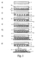
- Fig. 1 shows a diagram of the method according to the invention for manufacturing an antenna structure, with reference to which the invention will be explained below.
- a process support 1 is provided which has sufficient resistance to mechanical, thermal and chemical stress. Suitable materials for the process support 1 include, for example, copper, steel, aluminum or alloys comprising the aforementioned materials as a constituent.
- a process support coating 2 Applied to a work surface 1 a of the process support 1 in step b) is a process support coating 2, the thickness D of which corresponds approximately to the thickness of the antenna structure to be manufactured and typically lies in a range from a few ⁇ m to a few tenths of a mm.
- Suitable materials for the process support coating 2 include, for example, varnishes, polytetrafluoroethylene (PTFE) layers, and plastic films and sheets.
- a negative 3 of the antenna structure to be manufactured is made in the process support coating 2 by removing regions of the process support coating 2 which correspond to the contours of the antenna structure.
- the corresponding regions of the process support coating 2 may be removed by chemical (e.g. etching) or mechanical processes, wherein mechanical processes include for example cutting (including laser cutting), milling and stamping. It should be mentioned that according to the invention it is also possible to swap the temporal order of method steps b) and c).
- stamping operation is carried out first and then the process support coating 2 containing the negative 3 is applied to the process support 1.
- a release agent 4 is then introduced into the negative antenna structure 3 of the process support coating.
- the release agent 4 makes it possible to detach the finished antenna structure from the process support 1 and from the process support coating 2 in a subsequent method step.
- Graphite powder has proven to be an advantageous material for the release agent 4.
- step e) of the antenna structure manufacturing method according to the invention an electrically conductive antenna material 5 is introduced into the negative antenna structure 3 of the process support coating 2, possibly followed by curing of the antenna material 5.
- the introduction of the electrically conductive antenna material 5 into the negative antenna structure 3 may preferably take place by an electroplating process shown schematically in Fig. 2.
- the complex consisting of the process support 1 and the process support coating 2 containing the negative antenna structure is dipped into an electrolyte basin 10 which contains an electrolyte liquid 11.
- the process support 1 is designed as a cylinder.
- a DC voltage source 12 is connected by its negative pole to the process support 1 and by its positive pole to the electrolyte liquid 11, which contains dissolved particles (ions) of the antenna material 5.
- the ions of the antenna material 5 which are contained in the electrolyte liquid 11 migrate toward the negative antenna structure 3 and accumulate therein.
- the antenna material 5 comprises very highly electrically conductive materials, preferably metals such as copper or aluminum.
- the process support 1 and the release agent 4 must consist of electrically conductive material
- the process support coating 2 consists of electrically insulating material.
- the production of a negative 3 of the antenna structure in the process support coating 2 is carried out in such a way that the regions of the process support coating 2 which define the antenna structure to be produced are removed through the entire thickness D of the process support coating 2, so that in these regions the work surface 1a of the process support 1 is exposed and can be covered by the conductive release agent 4. Since an electrically conductive contact thus exists in the negative antenna structure 3 between the release agent 4 and the electrolyte liquid 11, electroplating of the antenna material 5 into the negative antenna structure 3 is ensured.
- Fig. 3 schematically shows an alternative embodiment of step e) of introducing the electrically conductive antenna material 5 into the negative antenna structure 3.
- the electrically conductive antenna material 5 is introduced into the negative antenna structure 3 of the process support coating 2 in the form of a solder paste, possibly even a solder powder, wherein the introduction may take place by printing, injection or the like.
- the solder paste has excellent electrical conductivity and therefore does not have to be subsequently coated with other conductive materials.
- the solder paste distributes uniformly in the negative antenna structure 3, it is heated to above its melting point (schematically shown by exposure to thermal radiation T from the electric heating unit 13) and then cured by cooling.
- the next step in the antenna structure manufacturing method according to the invention is the application of an adhesive 6 to the antenna material 5 (shown as step f1 in the figure) and the pressing of an antenna substrate 7 onto the exposed surfaces of the adhesive 6.
- the adhesive may advantageously be applied by a roller process.
- the type of adhesive is not restricted by any greater detail; by way of example, use may be made of dry adhesives, pressure adhesives, films which exert an adhesive force at an increased temperature (heat-sealing films), liquid adhesives or UV-curing adhesives.
- the adhesive 6 may also first be applied to the antenna substrate 7, and then the assembly consisting of antenna substrate 7 and adhesive is stuck onto the antenna material 5.
- Suitable materials for the antenna substrate 7 include, for example, paper and plastic films or sheets which are made of PVC, PA, PE or the like. Fabrics are also suitable as antenna substrate 7, so that the antenna structure according to the invention can also be installed in labels.
- the adhesive force which binds the release agent 4 to the process support 1 and to the process support coating 2 on the one hand and to the antenna material 5 on the other hand can be set either such that the release agent 4 is also pulled off when the antenna material 5 designed as an antenna structure is pulled off the process support 1, or such that the release agent 4 remains on the process support 1 and possibly on the process support coating 2 when the antenna material 5 designed as an antenna structure is pulled off the process support 1.
- the release agent 4 can be used for the successive manufacture of a number of antenna structures.
- Fig. 4 shows in plan view an RFID data carrier 14 which is arranged on a data carrier substrate 15 and is connected to an antenna structure 16 which has been manufactured in accordance with the antenna structure manufacturing method according to the invention.
- the antenna structure 16 may be situated on a dedicated antenna substrate which is connected to the data carrier substrate 15.
- the data carrier substrate 15 is advantageously also used as an antenna substrate for the antenna structure 16.
Landscapes
- Engineering & Computer Science (AREA)
- Computer Hardware Design (AREA)
- Microelectronics & Electronic Packaging (AREA)
- Physics & Mathematics (AREA)
- General Physics & Mathematics (AREA)
- Theoretical Computer Science (AREA)
- Details Of Aerials (AREA)
- Support Of Aerials (AREA)
Abstract
Description
- The invention relates to a method of manufacturing an antenna structure.
- The invention furthermore relates to a data carrier.
- It is known to manufacture antennas of contactless data carriers, such as smart cards for example, by means of an etching method in which, from a substrate which on one surface has an electrically conductive material, such as copper or aluminum for example, all those regions of the conductive material which do not form part of the antenna structure to be formed are etched away, and the remaining part of the conductive material forms the antenna structure. To this end, firstly the regions of the electrically conductive material which are to form the antenna structure are covered with an acid-resistant photoresist or the like, and then the conductive material is brought into contact with acid in order to carry out the etching operation. Since material is removed in this manufacturing method, it is referred to as a "subtractive" process. A further example of a subtractive process which may be mentioned is the antenna stamping method described in the document
US-20030112202 A1 , in which the antenna is stamped out of a flat, electrically conductive composite foil by means of a stamping tool, the cutting edges of which define the contours of the antenna that is to be manufactured. - It is furthermore known to print an antenna onto an electrically insulating substrate, wherein the printing material is a silver paste which has a relatively high specific resistance, and in a second step to apply a highly conductive material, such as copper for example, to the printed silver paste by means of electroplating, in order to achieve an overall sufficiently good electrical conductivity of the antenna. One problem here, however, is that during the electroplating operation, on account of the considerable length of the antenna (up to 1 m) and the relatively high specific electrical resistance of the silver paste, much more material accumulates at the ends of the antenna than in the central region thereof. Since, in this process for manufacturing an antenna structure, material is added to the base substrate, this is referred to as an "additive" process. In order to alleviate the disadvantage of unequal current distribution in the antenna in the case of the aforementioned additive manufacturing process, it is proposed in the document
US-20030011523 A1 , for the purpose of better current distribution in the antenna, to fix a temporary short-circuit clip across the windings of the antenna structure during the electroplating operation and to remove the short-circuit clip once electroplating is complete. Despite this measure, the current distribution in the antenna structure is still not optimal, and mass production with large substrate widths is difficult. A further disadvantage of this known method of manufacturing an antenna structure is that work has to be carried out directly on the substrate, and this increases the risk of faults. - In another document:
US 2003/091789-A1 , this discloses a method for making conductive circuits using powdered metals. - It is an object of the invention to provide a method of manufacturing an antenna structure of the type mentioned in the first paragraph and a data carrier of the type mentioned in the second paragraph, in which the abovementioned disadvantages are avoided.
- In order to achieve the abovementioned object, an antenna structure manufacturing method according to the invention is provided with features according to the invention so that a method according to the invention can be characterized as follows, namely:
- A method of manufacturing an antenna structure, which method comprises:
- a) providing a process support,
- b) applying a process support coating to a work surface of the process support,
- c) producing a negative of the antenna structure in the process support coating by removing corresponding regions of the process support coating along the contours of the antenna structure to be produced,
- d) introducing a release agent into the negative antenna structure of the process support coating,
- e) introducing an electrically conductive antenna material into the negative antenna structure of the process support coating, optionally followed by curing of the antenna material,
- f) joining the antenna material to an antenna substrate by means of an adhesive,
- g) pulling the antenna structure off the process support, said antenna structure being joined to the antenna substrate and made of the antenna material.
- In order to achieve the abovementioned object, such a data carrier is provided with an antenna structure manufactured in accordance with the antenna structure manufacturing method according to the invention.
- By virtue of the features according to the invention, only a small amount of material has to be removed during manufacture of the antenna structure. The antenna structure manufacturing method according to the invention is an additive method. Unlike in the known additive methods, however, a uniform amount of electrically conductive material is applied over the entire length of the antenna without the use of additional aids, such as short-circuit clips. The antenna structure manufacturing method according to the invention can moreover be implemented as a continuous manufacturing method in mass industrial processes.
- It may be mentioned that the document
WO 03/107266 A1 - According to the measures of
claim 2, the advantage is obtained that the release agent remains on the surface of the antenna structure and can act as a protective layer for the antenna structure. - According to the measures of
claim 3, the advantage is obtained that the release agent can be used to manufacture a large number of antennas, and this ensures a highly resource-saving manufacturing method. - According to the measures of
claim 4, the advantage is obtained that the electrically conductive antenna material can be introduced by means of a technologically perfected electroplating process. - According to the measures of
claim 5, the advantage is obtained that the introduction of the electrically conductive antenna material takes place very quickly, and the antenna structure can thus be manufactured within a short period of time. - According to the measures of
claim 6, the advantage is obtained that the antenna structure manufacturing method can be configured as a rotation process, and this means a very high manufacturing speed while the machine takes up a small amount of space. - According to the measures of claim 8, the advantage is obtained that the method can be carried out with a high saving in terms of material, and thus cost-effectively.
- The abovementioned and other aspects of the invention will emerge from the example of embodiment described below and will be explained with reference to this example of embodiment.
- The invention will be further described with reference to an example of embodiment shown in the drawings to which, however, the invention is not restricted.
- Fig. 1 shows a diagram of the method according to the invention for manufacturing an antenna structure.
- Fig. 2 schematically shows the method step of introducing an electrically conductive antenna material by means of an electroplating process.
- Fig. 3 schematically shows a further embodiment of the method step of introducing an electrically conductive antenna material.
- Fig. 4 shows a plan view of an RFID data carrier comprising an antenna structure manufactured according to the invention.
- Fig. 1 shows a diagram of the method according to the invention for manufacturing an antenna structure, with reference to which the invention will be explained below. In step a) of the antenna structure manufacturing method according to the invention, a
process support 1 is provided which has sufficient resistance to mechanical, thermal and chemical stress. Suitable materials for theprocess support 1 include, for example, copper, steel, aluminum or alloys comprising the aforementioned materials as a constituent. Applied to awork surface 1 a of theprocess support 1 in step b) is aprocess support coating 2, the thickness D of which corresponds approximately to the thickness of the antenna structure to be manufactured and typically lies in a range from a few µm to a few tenths of a mm. The requirement of sufficient resistance to mechanical, thermal and chemical stress during the method also applies in respect of theprocess support coating 2. Suitable materials for theprocess support coating 2 include, for example, varnishes, polytetrafluoroethylene (PTFE) layers, and plastic films and sheets. In step c), a negative 3 of the antenna structure to be manufactured is made in theprocess support coating 2 by removing regions of theprocess support coating 2 which correspond to the contours of the antenna structure. The corresponding regions of theprocess support coating 2 may be removed by chemical (e.g. etching) or mechanical processes, wherein mechanical processes include for example cutting (including laser cutting), milling and stamping. It should be mentioned that according to the invention it is also possible to swap the temporal order of method steps b) and c). Especially when stamping the negative 3 of the antenna structure to be manufactured in aprocess support coating 2 formed by a plastic film or a plastic sheet, the stamping operation is carried out first and then theprocess support coating 2 containing the negative 3 is applied to theprocess support 1. - In step d), a
release agent 4 is then introduced into thenegative antenna structure 3 of the process support coating. Therelease agent 4 makes it possible to detach the finished antenna structure from theprocess support 1 and from theprocess support coating 2 in a subsequent method step. Graphite powder has proven to be an advantageous material for therelease agent 4. - In step e) of the antenna structure manufacturing method according to the invention, an electrically
conductive antenna material 5 is introduced into thenegative antenna structure 3 of theprocess support coating 2, possibly followed by curing of theantenna material 5. - The introduction of the electrically
conductive antenna material 5 into thenegative antenna structure 3 may preferably take place by an electroplating process shown schematically in Fig. 2. The complex consisting of theprocess support 1 and theprocess support coating 2 containing the negative antenna structure is dipped into anelectrolyte basin 10 which contains anelectrolyte liquid 11. Theprocess support 1 is designed as a cylinder. ADC voltage source 12 is connected by its negative pole to theprocess support 1 and by its positive pole to theelectrolyte liquid 11, which contains dissolved particles (ions) of theantenna material 5. By virtue of the application of the electrical voltage, the ions of theantenna material 5 which are contained in theelectrolyte liquid 11 migrate toward thenegative antenna structure 3 and accumulate therein. Theantenna material 5 comprises very highly electrically conductive materials, preferably metals such as copper or aluminum. In order for it to be possible for the described electroplating method to be carried out, the following prerequisites must be satisfied: Theprocess support 1 and therelease agent 4 must consist of electrically conductive material, whereas theprocess support coating 2 consists of electrically insulating material. The production of a negative 3 of the antenna structure in theprocess support coating 2 is carried out in such a way that the regions of theprocess support coating 2 which define the antenna structure to be produced are removed through the entire thickness D of theprocess support coating 2, so that in these regions thework surface 1a of theprocess support 1 is exposed and can be covered by theconductive release agent 4. Since an electrically conductive contact thus exists in thenegative antenna structure 3 between therelease agent 4 and theelectrolyte liquid 11, electroplating of theantenna material 5 into thenegative antenna structure 3 is ensured. - Fig. 3 schematically shows an alternative embodiment of step e) of introducing the electrically
conductive antenna material 5 into thenegative antenna structure 3. The electricallyconductive antenna material 5 is introduced into thenegative antenna structure 3 of theprocess support coating 2 in the form of a solder paste, possibly even a solder powder, wherein the introduction may take place by printing, injection or the like. Unlike the silver paste used in the prior art, the solder paste has excellent electrical conductivity and therefore does not have to be subsequently coated with other conductive materials. In order that the solder paste distributes uniformly in thenegative antenna structure 3, it is heated to above its melting point (schematically shown by exposure to thermal radiation T from the electric heating unit 13) and then cured by cooling. It should be mentioned that, in this variant of the method step of introducing the electricallyconductive antenna material 5 into thenegative antenna structure 3, it is not necessary for theprocess support 1 and/or therelease agent 4 to be electrically conductive, since no electroplating is carried out. It is also not necessary for theprocess support coating 2 to be electrically insulating. - Returning now to Fig. 1, the next step in the antenna structure manufacturing method according to the invention is the application of an adhesive 6 to the antenna material 5 (shown as step f1 in the figure) and the pressing of an
antenna substrate 7 onto the exposed surfaces of the adhesive 6. The adhesive may advantageously be applied by a roller process. The type of adhesive is not restricted by any greater detail; by way of example, use may be made of dry adhesives, pressure adhesives, films which exert an adhesive force at an increased temperature (heat-sealing films), liquid adhesives or UV-curing adhesives. It should be mentioned that according to the invention the adhesive 6 may also first be applied to theantenna substrate 7, and then the assembly consisting ofantenna substrate 7 and adhesive is stuck onto theantenna material 5. Suitable materials for theantenna substrate 7 include, for example, paper and plastic films or sheets which are made of PVC, PA, PE or the like. Fabrics are also suitable asantenna substrate 7, so that the antenna structure according to the invention can also be installed in labels. - The antenna structure manufacturing method according to the invention is then completed by step g) of pulling the
antenna structure 16 off theprocess support 1, said antenna structure being joined to theantenna substrate 7 and being formed by theantenna material 5. - Returning once again to step d) of the antenna structure manufacturing method according to the invention, it should be mentioned that the adhesive force which binds the
release agent 4 to theprocess support 1 and to theprocess support coating 2 on the one hand and to theantenna material 5 on the other hand can be set either such that therelease agent 4 is also pulled off when theantenna material 5 designed as an antenna structure is pulled off theprocess support 1, or such that therelease agent 4 remains on theprocess support 1 and possibly on theprocess support coating 2 when theantenna material 5 designed as an antenna structure is pulled off theprocess support 1. In the latter case, therelease agent 4 can be used for the successive manufacture of a number of antenna structures. - Fig. 4 shows in plan view an
RFID data carrier 14 which is arranged on adata carrier substrate 15 and is connected to anantenna structure 16 which has been manufactured in accordance with the antenna structure manufacturing method according to the invention. Theantenna structure 16 may be situated on a dedicated antenna substrate which is connected to thedata carrier substrate 15. However, thedata carrier substrate 15 is advantageously also used as an antenna substrate for theantenna structure 16.
Claims (8)
- A method of manufacturing an antenna structure (16) for RFID, which method comprises:a) providing a process support (1),b) applying a process support coating (2) to a work surface (1a) of the process support (1),c) producing a negative (3) of the antenna structure in the process support coating (2) by removing corresponding regions of the process support coating along the contours of the antenna structure to be produced,
and characterized byd) introducing a release agent (4) into the negative antenna structure (3) of the process support coating,e) introducing an electrically conductive antenna material (5) into the negative antenna structure (3) of the process support coating (2), optionally followed by curing of the antenna material (5),f) joining the antenna material (5) to an antenna substrate (7) by means of an adhesive (6), 'g) pulling the antenna structure (16) off the process support (1), said antenna structure being joined to the antenna substrate (7) and made of the antenna material (5). - An antenna structure manufacturing method as claimed in claim 1, wherein the release agent (4) is also pulled off when the antenna structure (16) is pulled off the process support (1).
- An antenna structure manufacturing method as claimed in claim 1, wherein the release agent (4) remains on the process support (1) and possibly on the process support coating (2) when the antenna structure (16) is pulled off the process support (1).
- An antenna structure manufacturing method as claimed in claim 1, wherein the process support (1) and the release agent (4) are electrically conductive, the process support coating (2) is electrically insulating, the production of a negative (3) of the antenna structure in the process support coating (2) comprises removing corresponding regions of the process support coating, according to the antenna structure to be produced, down to the process support work surface (1a), the release agent (4) is applied to the process support work surface (1a), and the introduction of the electrically conductive antenna material (5) into the negative antenna structure (3) comprises electroplating the antenna material (5) into the negative antenna structure.
- An antenna structure manufacturing method as claimed in claim 1, wherein the introduction of an electrically conductive antenna material (5) into the negative antenna structure (3) of the process support coating (2) comprises introducing a solder paste, melting the solder paste in order to distribute it uniformly in the negative antenna structure, and curing the molten solder paste.
- An antenna structure manufacturing method as claimed in claim 1, wherein the process support (1) is designed as a cylinder.
- A data carrier (14), comprising an antenna structure (16) which is manufactured as claimed in any of claims 1 to 6.
- A data carrier as claimed in claim 7, comprising a data carrier substrate (15) which at the same time serves as antenna substrate.
Priority Applications (1)
| Application Number | Priority Date | Filing Date | Title |
|---|---|---|---|
| EP05774628A EP1789912B1 (en) | 2004-08-31 | 2005-08-17 | Method of manufacturing an rfid antenna |
Applications Claiming Priority (3)
| Application Number | Priority Date | Filing Date | Title |
|---|---|---|---|
| EP04104159 | 2004-08-31 | ||
| PCT/IB2005/052709 WO2006024980A1 (en) | 2004-08-31 | 2005-08-17 | Method of manufacturing an rfid antenna |
| EP05774628A EP1789912B1 (en) | 2004-08-31 | 2005-08-17 | Method of manufacturing an rfid antenna |
Publications (2)
| Publication Number | Publication Date |
|---|---|
| EP1789912A1 EP1789912A1 (en) | 2007-05-30 |
| EP1789912B1 true EP1789912B1 (en) | 2008-01-23 |
Family
ID=35079461
Family Applications (1)
| Application Number | Title | Priority Date | Filing Date |
|---|---|---|---|
| EP05774628A Expired - Lifetime EP1789912B1 (en) | 2004-08-31 | 2005-08-17 | Method of manufacturing an rfid antenna |
Country Status (7)
| Country | Link |
|---|---|
| US (1) | US20100026442A1 (en) |
| EP (1) | EP1789912B1 (en) |
| JP (1) | JP2008512019A (en) |
| CN (1) | CN100504917C (en) |
| AT (1) | ATE385001T1 (en) |
| DE (1) | DE602005004562T2 (en) |
| WO (1) | WO2006024980A1 (en) |
Families Citing this family (4)
| Publication number | Priority date | Publication date | Assignee | Title |
|---|---|---|---|---|
| US7605056B2 (en) * | 2005-05-31 | 2009-10-20 | Semiconductor Energy Laboratory Co., Ltd. | Method of manufacturing a semiconductor device including separation by physical force |
| DE102006054449A1 (en) * | 2006-11-16 | 2008-05-21 | Smartrac Ip B.V. | transponder unit |
| KR100999798B1 (en) * | 2010-02-11 | 2010-12-08 | 엘지이노텍 주식회사 | Semiconductor light emitting device and manufacturing method thereof |
| FR2962579A1 (en) * | 2010-07-12 | 2012-01-13 | Ask Sa | RADIO FREQUENCY IDENTIFICATION DEVICE OF POLYCARBONATE AND METHOD OF MANUFACTURING THE SAME |
Family Cites Families (21)
| Publication number | Priority date | Publication date | Assignee | Title |
|---|---|---|---|---|
| US2963748A (en) * | 1957-05-27 | 1960-12-13 | Young Lawrence John | Printed circuits |
| JPH02141233A (en) * | 1988-11-22 | 1990-05-30 | Toyo Metaraijingu Kk | Laminated transfer film for printed wiring board |
| JPH05309963A (en) * | 1992-05-14 | 1993-11-22 | Matsushita Electric Ind Co Ltd | Intaglio for printing and method for printing |
| JPH06181380A (en) * | 1992-06-02 | 1994-06-28 | Ibiden Co Ltd | Surface mounting substrate and manufacture thereof |
| JPH06183165A (en) * | 1992-12-18 | 1994-07-05 | Fujitsu Ltd | Metal mask and manufacturing method thereof |
| JPH09139564A (en) * | 1995-11-15 | 1997-05-27 | Dainippon Printing Co Ltd | Thick film wiring and method of forming the same |
| DE19637018A1 (en) * | 1996-09-12 | 1998-03-19 | Bayer Ag | Process for the production of rigid and flexible circuits |
| JP3697859B2 (en) * | 1997-10-06 | 2005-09-21 | 松下電器産業株式会社 | Manufacturing method of fine pattern |
| FR2761497B1 (en) * | 1997-03-27 | 1999-06-18 | Gemplus Card Int | METHOD FOR MANUFACTURING A CHIP CARD OR THE LIKE |
| JPH11135919A (en) * | 1997-10-27 | 1999-05-21 | Dainippon Printing Co Ltd | Circuit pattern forming method, circuit pattern forming sheet, and circuit pattern |
| US6618939B2 (en) * | 1998-02-27 | 2003-09-16 | Kabushiki Kaisha Miyake | Process for producing resonant tag |
| US6320556B1 (en) * | 2000-01-19 | 2001-11-20 | Moore North America, Inc. | RFID foil or film antennas |
| US6476775B1 (en) * | 2000-03-13 | 2002-11-05 | Rcd Technology Corporation | Method for forming radio frequency antenna |
| DE10016037B4 (en) * | 2000-03-31 | 2005-01-05 | Interlock Ag | Method for producing a label or a chip card |
| EP1191127B1 (en) * | 2000-09-26 | 2004-10-13 | Enthone-OMI (Deutschland) GmbH | Process for selective metallization of dielectric materials |
| EP1415270B1 (en) * | 2001-07-31 | 2016-08-03 | Quotainne Enterprises LLC | Data carrier comprising an array of contacts |
| US6805940B2 (en) * | 2001-09-10 | 2004-10-19 | 3M Innovative Properties Company | Method for making conductive circuits using powdered metals |
| JP4106237B2 (en) * | 2002-05-22 | 2008-06-25 | 株式会社アルバック | Method for peeling a deposited film on a substrate |
| FR2841089B1 (en) * | 2002-06-14 | 2004-07-30 | Sequoias | METHOD OF INDUSTRIAL MANUFACTURE OF ANTENNAS FOR RFID TRANSPONDERS |
| KR100581221B1 (en) * | 2004-06-30 | 2006-05-22 | 삼성전자주식회사 | Tape wiring board manufacturing method |
| DE102005016511B4 (en) * | 2005-04-11 | 2008-09-25 | Fraunhofer-Gesellschaft zur Förderung der angewandten Forschung e.V. | Method for producing a conductor structure on a substrate |
-
2005
- 2005-08-17 WO PCT/IB2005/052709 patent/WO2006024980A1/en not_active Ceased
- 2005-08-17 AT AT05774628T patent/ATE385001T1/en not_active IP Right Cessation
- 2005-08-17 DE DE602005004562T patent/DE602005004562T2/en not_active Expired - Lifetime
- 2005-08-17 JP JP2007529070A patent/JP2008512019A/en active Pending
- 2005-08-17 CN CNB2005800370826A patent/CN100504917C/en not_active Expired - Fee Related
- 2005-08-17 EP EP05774628A patent/EP1789912B1/en not_active Expired - Lifetime
- 2005-08-17 US US11/574,243 patent/US20100026442A1/en not_active Abandoned
Also Published As
| Publication number | Publication date |
|---|---|
| DE602005004562D1 (en) | 2008-03-13 |
| US20100026442A1 (en) | 2010-02-04 |
| DE602005004562T2 (en) | 2009-01-22 |
| CN101048787A (en) | 2007-10-03 |
| ATE385001T1 (en) | 2008-02-15 |
| WO2006024980A1 (en) | 2006-03-09 |
| CN100504917C (en) | 2009-06-24 |
| EP1789912A1 (en) | 2007-05-30 |
| JP2008512019A (en) | 2008-04-17 |
Similar Documents
| Publication | Publication Date | Title |
|---|---|---|
| US7477194B2 (en) | Conductive pattern and method of making | |
| FI121592B (en) | Process for making PCB laminates, especially RFID antenna laminates and PCB laminates | |
| CN101663678B (en) | Chip module for an RFID system | |
| CN104868244B (en) | The production method of RFID paper substrate aluminum antennas | |
| US4091125A (en) | Circuit board and method for producing same | |
| KR101468243B1 (en) | RFID system, especially self-adhesive antenna for RFID label, and manufacturing method thereof | |
| CN101375463A (en) | Component including radio frequency (RF) antenna and method of manufacturing the same | |
| US4313995A (en) | Circuit board and method for producing same | |
| CN101316001B (en) | Method for producing radio frequency label antenna | |
| JPH0225274B2 (en) | ||
| CN103004293B (en) | Multilayer Thin Film Components | |
| EP1486996A1 (en) | Method of manufacturing a plane coil | |
| US20070082127A1 (en) | Process for producing a structured metal layer on a substrate body | |
| CN104411099B (en) | Transfer method for circuitous pattern of heavy copper printed circuit board | |
| CN102035074B (en) | Method for manufacturing radio frequency identification (RFID) tag antenna | |
| US20200071160A1 (en) | Method for forming microstructures | |
| US20100026442A1 (en) | Method of manufacturing an RFID antenna | |
| CN109769350A (en) | A kind of single-sided circuit board and preparation method of thermally conductive insulating adhesive film | |
| EP0476867B1 (en) | Method using a permanent mandrel for manufacture of electrical circuitry | |
| EP1030328A3 (en) | Method and apparatus for manufacutring solid electrolytic capacitor | |
| JPWO2011067851A1 (en) | Crimp-type metal decorative plate, metal decorative plate, and manufacturing method thereof | |
| CN102339665B (en) | Manufacturing method of alloy resistor | |
| US6632341B1 (en) | Method for producing a self-supporting metal film | |
| CN115377624A (en) | Method of forming edge material on electrochemical cell assembly | |
| RU2791713C1 (en) | Method for manufacturing flexible printed circuit boards in continuous roll form |
Legal Events
| Date | Code | Title | Description |
|---|---|---|---|
| PUAI | Public reference made under article 153(3) epc to a published international application that has entered the european phase |
Free format text: ORIGINAL CODE: 0009012 |
|
| 17P | Request for examination filed |
Effective date: 20070402 |
|
| AK | Designated contracting states |
Kind code of ref document: A1 Designated state(s): AT BE BG CH CY CZ DE DK EE ES FI FR GB GR HU IE IS IT LI LT LU LV MC NL PL PT RO SE SI SK TR |
|
| GRAP | Despatch of communication of intention to grant a patent |
Free format text: ORIGINAL CODE: EPIDOSNIGR1 |
|
| DAX | Request for extension of the european patent (deleted) | ||
| GRAS | Grant fee paid |
Free format text: ORIGINAL CODE: EPIDOSNIGR3 |
|
| GRAA | (expected) grant |
Free format text: ORIGINAL CODE: 0009210 |
|
| AK | Designated contracting states |
Kind code of ref document: B1 Designated state(s): AT BE BG CH CY CZ DE DK EE ES FI FR GB GR HU IE IS IT LI LT LU LV MC NL PL PT RO SE SI SK TR |
|
| AX | Request for extension of the european patent |
Extension state: AL BA HR MK YU |
|
| RAX | Requested extension states of the european patent have changed |
Extension state: MK Payment date: 20070402 Extension state: BA Payment date: 20070402 Extension state: YU Payment date: 20070402 Extension state: AL Payment date: 20070402 Extension state: HR Payment date: 20070402 |
|
| REG | Reference to a national code |
Ref country code: GB Ref legal event code: FG4D |
|
| REG | Reference to a national code |
Ref country code: CH Ref legal event code: EP |
|
| REG | Reference to a national code |
Ref country code: IE Ref legal event code: FG4D |
|
| REF | Corresponds to: |
Ref document number: 602005004562 Country of ref document: DE Date of ref document: 20080313 Kind code of ref document: P |
|
| NLV1 | Nl: lapsed or annulled due to failure to fulfill the requirements of art. 29p and 29m of the patents act | ||
| PG25 | Lapsed in a contracting state [announced via postgrant information from national office to epo] |
Ref country code: CH Free format text: LAPSE BECAUSE OF FAILURE TO SUBMIT A TRANSLATION OF THE DESCRIPTION OR TO PAY THE FEE WITHIN THE PRESCRIBED TIME-LIMIT Effective date: 20080123 Ref country code: LI Free format text: LAPSE BECAUSE OF FAILURE TO SUBMIT A TRANSLATION OF THE DESCRIPTION OR TO PAY THE FEE WITHIN THE PRESCRIBED TIME-LIMIT Effective date: 20080123 Ref country code: FI Free format text: LAPSE BECAUSE OF FAILURE TO SUBMIT A TRANSLATION OF THE DESCRIPTION OR TO PAY THE FEE WITHIN THE PRESCRIBED TIME-LIMIT Effective date: 20080123 Ref country code: IS Free format text: LAPSE BECAUSE OF FAILURE TO SUBMIT A TRANSLATION OF THE DESCRIPTION OR TO PAY THE FEE WITHIN THE PRESCRIBED TIME-LIMIT Effective date: 20080523 Ref country code: ES Free format text: LAPSE BECAUSE OF FAILURE TO SUBMIT A TRANSLATION OF THE DESCRIPTION OR TO PAY THE FEE WITHIN THE PRESCRIBED TIME-LIMIT Effective date: 20080504 |
|
| REG | Reference to a national code |
Ref country code: CH Ref legal event code: PL |
|
| PG25 | Lapsed in a contracting state [announced via postgrant information from national office to epo] |
Ref country code: BG Free format text: LAPSE BECAUSE OF FAILURE TO SUBMIT A TRANSLATION OF THE DESCRIPTION OR TO PAY THE FEE WITHIN THE PRESCRIBED TIME-LIMIT Effective date: 20080423 Ref country code: AT Free format text: LAPSE BECAUSE OF FAILURE TO SUBMIT A TRANSLATION OF THE DESCRIPTION OR TO PAY THE FEE WITHIN THE PRESCRIBED TIME-LIMIT Effective date: 20080123 |
|
| ET | Fr: translation filed | ||
| PG25 | Lapsed in a contracting state [announced via postgrant information from national office to epo] |
Ref country code: LV Free format text: LAPSE BECAUSE OF FAILURE TO SUBMIT A TRANSLATION OF THE DESCRIPTION OR TO PAY THE FEE WITHIN THE PRESCRIBED TIME-LIMIT Effective date: 20080123 Ref country code: PL Free format text: LAPSE BECAUSE OF FAILURE TO SUBMIT A TRANSLATION OF THE DESCRIPTION OR TO PAY THE FEE WITHIN THE PRESCRIBED TIME-LIMIT Effective date: 20080123 Ref country code: PT Free format text: LAPSE BECAUSE OF FAILURE TO SUBMIT A TRANSLATION OF THE DESCRIPTION OR TO PAY THE FEE WITHIN THE PRESCRIBED TIME-LIMIT Effective date: 20080623 Ref country code: SI Free format text: LAPSE BECAUSE OF FAILURE TO SUBMIT A TRANSLATION OF THE DESCRIPTION OR TO PAY THE FEE WITHIN THE PRESCRIBED TIME-LIMIT Effective date: 20080123 Ref country code: BE Free format text: LAPSE BECAUSE OF FAILURE TO SUBMIT A TRANSLATION OF THE DESCRIPTION OR TO PAY THE FEE WITHIN THE PRESCRIBED TIME-LIMIT Effective date: 20080123 |
|
| RAP2 | Party data changed (patent owner data changed or rights of a patent transferred) |
Owner name: NXP B.V. |
|
| PG25 | Lapsed in a contracting state [announced via postgrant information from national office to epo] |
Ref country code: CZ Free format text: LAPSE BECAUSE OF FAILURE TO SUBMIT A TRANSLATION OF THE DESCRIPTION OR TO PAY THE FEE WITHIN THE PRESCRIBED TIME-LIMIT Effective date: 20080123 Ref country code: DK Free format text: LAPSE BECAUSE OF FAILURE TO SUBMIT A TRANSLATION OF THE DESCRIPTION OR TO PAY THE FEE WITHIN THE PRESCRIBED TIME-LIMIT Effective date: 20080123 Ref country code: SE Free format text: LAPSE BECAUSE OF FAILURE TO SUBMIT A TRANSLATION OF THE DESCRIPTION OR TO PAY THE FEE WITHIN THE PRESCRIBED TIME-LIMIT Effective date: 20080423 Ref country code: SK Free format text: LAPSE BECAUSE OF FAILURE TO SUBMIT A TRANSLATION OF THE DESCRIPTION OR TO PAY THE FEE WITHIN THE PRESCRIBED TIME-LIMIT Effective date: 20080123 Ref country code: NL Free format text: LAPSE BECAUSE OF FAILURE TO SUBMIT A TRANSLATION OF THE DESCRIPTION OR TO PAY THE FEE WITHIN THE PRESCRIBED TIME-LIMIT Effective date: 20080123 |
|
| RAP2 | Party data changed (patent owner data changed or rights of a patent transferred) |
Owner name: NXP B.V. |
|
| PG25 | Lapsed in a contracting state [announced via postgrant information from national office to epo] |
Ref country code: RO Free format text: LAPSE BECAUSE OF FAILURE TO SUBMIT A TRANSLATION OF THE DESCRIPTION OR TO PAY THE FEE WITHIN THE PRESCRIBED TIME-LIMIT Effective date: 20080123 |
|
| PLBE | No opposition filed within time limit |
Free format text: ORIGINAL CODE: 0009261 |
|
| STAA | Information on the status of an ep patent application or granted ep patent |
Free format text: STATUS: NO OPPOSITION FILED WITHIN TIME LIMIT |
|
| 26N | No opposition filed |
Effective date: 20081024 |
|
| PG25 | Lapsed in a contracting state [announced via postgrant information from national office to epo] |
Ref country code: LT Free format text: LAPSE BECAUSE OF FAILURE TO SUBMIT A TRANSLATION OF THE DESCRIPTION OR TO PAY THE FEE WITHIN THE PRESCRIBED TIME-LIMIT Effective date: 20080123 |
|
| PG25 | Lapsed in a contracting state [announced via postgrant information from national office to epo] |
Ref country code: MC Free format text: LAPSE BECAUSE OF NON-PAYMENT OF DUE FEES Effective date: 20080831 |
|
| REG | Reference to a national code |
Ref country code: GB Ref legal event code: 732E Free format text: REGISTERED BETWEEN 20090305 AND 20090311 |
|
| PG25 | Lapsed in a contracting state [announced via postgrant information from national office to epo] |
Ref country code: EE Free format text: LAPSE BECAUSE OF FAILURE TO SUBMIT A TRANSLATION OF THE DESCRIPTION OR TO PAY THE FEE WITHIN THE PRESCRIBED TIME-LIMIT Effective date: 20080123 |
|
| PG25 | Lapsed in a contracting state [announced via postgrant information from national office to epo] |
Ref country code: CY Free format text: LAPSE BECAUSE OF FAILURE TO SUBMIT A TRANSLATION OF THE DESCRIPTION OR TO PAY THE FEE WITHIN THE PRESCRIBED TIME-LIMIT Effective date: 20080123 Ref country code: IE Free format text: LAPSE BECAUSE OF NON-PAYMENT OF DUE FEES Effective date: 20080818 |
|
| PG25 | Lapsed in a contracting state [announced via postgrant information from national office to epo] |
Ref country code: IT Free format text: LAPSE BECAUSE OF FAILURE TO SUBMIT A TRANSLATION OF THE DESCRIPTION OR TO PAY THE FEE WITHIN THE PRESCRIBED TIME-LIMIT Effective date: 20080123 |
|
| REG | Reference to a national code |
Ref country code: FR Ref legal event code: TP |
|
| PG25 | Lapsed in a contracting state [announced via postgrant information from national office to epo] |
Ref country code: LU Free format text: LAPSE BECAUSE OF NON-PAYMENT OF DUE FEES Effective date: 20080817 Ref country code: HU Free format text: LAPSE BECAUSE OF FAILURE TO SUBMIT A TRANSLATION OF THE DESCRIPTION OR TO PAY THE FEE WITHIN THE PRESCRIBED TIME-LIMIT Effective date: 20080724 |
|
| PG25 | Lapsed in a contracting state [announced via postgrant information from national office to epo] |
Ref country code: TR Free format text: LAPSE BECAUSE OF FAILURE TO SUBMIT A TRANSLATION OF THE DESCRIPTION OR TO PAY THE FEE WITHIN THE PRESCRIBED TIME-LIMIT Effective date: 20080123 |
|
| PG25 | Lapsed in a contracting state [announced via postgrant information from national office to epo] |
Ref country code: GR Free format text: LAPSE BECAUSE OF FAILURE TO SUBMIT A TRANSLATION OF THE DESCRIPTION OR TO PAY THE FEE WITHIN THE PRESCRIBED TIME-LIMIT Effective date: 20080424 |
|
| PGFP | Annual fee paid to national office [announced via postgrant information from national office to epo] |
Ref country code: GB Payment date: 20120725 Year of fee payment: 8 |
|
| PGFP | Annual fee paid to national office [announced via postgrant information from national office to epo] |
Ref country code: FR Payment date: 20120906 Year of fee payment: 8 Ref country code: DE Payment date: 20120723 Year of fee payment: 8 |
|
| GBPC | Gb: european patent ceased through non-payment of renewal fee |
Effective date: 20130817 |
|
| PG25 | Lapsed in a contracting state [announced via postgrant information from national office to epo] |
Ref country code: DE Free format text: LAPSE BECAUSE OF NON-PAYMENT OF DUE FEES Effective date: 20140301 |
|
| REG | Reference to a national code |
Ref country code: FR Ref legal event code: ST Effective date: 20140430 |
|
| REG | Reference to a national code |
Ref country code: DE Ref legal event code: R119 Ref document number: 602005004562 Country of ref document: DE Effective date: 20140301 |
|
| PG25 | Lapsed in a contracting state [announced via postgrant information from national office to epo] |
Ref country code: GB Free format text: LAPSE BECAUSE OF NON-PAYMENT OF DUE FEES Effective date: 20130817 |
|
| PG25 | Lapsed in a contracting state [announced via postgrant information from national office to epo] |
Ref country code: FR Free format text: LAPSE BECAUSE OF NON-PAYMENT OF DUE FEES Effective date: 20130902 |