EP1787163B1 - Optical switch - Google Patents
Optical switch Download PDFInfo
- Publication number
- EP1787163B1 EP1787163B1 EP04772891A EP04772891A EP1787163B1 EP 1787163 B1 EP1787163 B1 EP 1787163B1 EP 04772891 A EP04772891 A EP 04772891A EP 04772891 A EP04772891 A EP 04772891A EP 1787163 B1 EP1787163 B1 EP 1787163B1
- Authority
- EP
- European Patent Office
- Prior art keywords
- clad layer
- node
- substrate
- core
- output lines
- Prior art date
- Legal status (The legal status is an assumption and is not a legal conclusion. Google has not performed a legal analysis and makes no representation as to the accuracy of the status listed.)
- Expired - Lifetime
Links
Images



Classifications
-
- G—PHYSICS
- G02—OPTICS
- G02F—OPTICAL DEVICES OR ARRANGEMENTS FOR THE CONTROL OF LIGHT BY MODIFICATION OF THE OPTICAL PROPERTIES OF THE MEDIA OF THE ELEMENTS INVOLVED THEREIN; NON-LINEAR OPTICS; FREQUENCY-CHANGING OF LIGHT; OPTICAL LOGIC ELEMENTS; OPTICAL ANALOGUE/DIGITAL CONVERTERS
- G02F1/00—Devices or arrangements for the control of the intensity, colour, phase, polarisation or direction of light arriving from an independent light source, e.g. switching, gating or modulating; Non-linear optics
- G02F1/29—Devices or arrangements for the control of the intensity, colour, phase, polarisation or direction of light arriving from an independent light source, e.g. switching, gating or modulating; Non-linear optics for the control of the position or the direction of light beams, i.e. deflection
- G02F1/31—Digital deflection, i.e. optical switching
- G02F1/313—Digital deflection, i.e. optical switching in an optical waveguide structure
- G02F1/3137—Digital deflection, i.e. optical switching in an optical waveguide structure with intersecting or branching waveguides, e.g. X-switches and Y-junctions
-
- G—PHYSICS
- G02—OPTICS
- G02F—OPTICAL DEVICES OR ARRANGEMENTS FOR THE CONTROL OF LIGHT BY MODIFICATION OF THE OPTICAL PROPERTIES OF THE MEDIA OF THE ELEMENTS INVOLVED THEREIN; NON-LINEAR OPTICS; FREQUENCY-CHANGING OF LIGHT; OPTICAL LOGIC ELEMENTS; OPTICAL ANALOGUE/DIGITAL CONVERTERS
- G02F1/00—Devices or arrangements for the control of the intensity, colour, phase, polarisation or direction of light arriving from an independent light source, e.g. switching, gating or modulating; Non-linear optics
- G02F1/01—Devices or arrangements for the control of the intensity, colour, phase, polarisation or direction of light arriving from an independent light source, e.g. switching, gating or modulating; Non-linear optics for the control of the intensity, phase, polarisation or colour
- G02F1/0147—Devices or arrangements for the control of the intensity, colour, phase, polarisation or direction of light arriving from an independent light source, e.g. switching, gating or modulating; Non-linear optics for the control of the intensity, phase, polarisation or colour based on thermo-optic effects
-
- G—PHYSICS
- G02—OPTICS
- G02F—OPTICAL DEVICES OR ARRANGEMENTS FOR THE CONTROL OF LIGHT BY MODIFICATION OF THE OPTICAL PROPERTIES OF THE MEDIA OF THE ELEMENTS INVOLVED THEREIN; NON-LINEAR OPTICS; FREQUENCY-CHANGING OF LIGHT; OPTICAL LOGIC ELEMENTS; OPTICAL ANALOGUE/DIGITAL CONVERTERS
- G02F1/00—Devices or arrangements for the control of the intensity, colour, phase, polarisation or direction of light arriving from an independent light source, e.g. switching, gating or modulating; Non-linear optics
- G02F1/01—Devices or arrangements for the control of the intensity, colour, phase, polarisation or direction of light arriving from an independent light source, e.g. switching, gating or modulating; Non-linear optics for the control of the intensity, phase, polarisation or colour
- G02F1/061—Devices or arrangements for the control of the intensity, colour, phase, polarisation or direction of light arriving from an independent light source, e.g. switching, gating or modulating; Non-linear optics for the control of the intensity, phase, polarisation or colour based on electro-optical organic material
- G02F1/065—Devices or arrangements for the control of the intensity, colour, phase, polarisation or direction of light arriving from an independent light source, e.g. switching, gating or modulating; Non-linear optics for the control of the intensity, phase, polarisation or colour based on electro-optical organic material in an optical waveguide structure
Definitions
- an optical device comprising a core layer; a first clad layer, with the core layer being deposited on a part of surface of the first clad layer; a second clad layer, with the core layer being provided between the first clad layer and the second clad layer; a third clad layer deposited on the second clad, an electrode for heating, and a substrate having a heat-sink function.
- At least one of the core layer and the clad layers comprises a material having a positive refractive index variation coefficient.
- the third clad layer has a refractive index smaller than that of the second clad layer.
- Each output line 33 includes a straight segment 35 that branches off from the node 32, a curved segment 36 extending from the straight segment 35, and a rear straight segment 37 extending from the curved segment 60 and terminating at an output terminal 93, which is connected to each of the output optical fibers 131 at the output connector 130.
- the curved segment 36 is introduced for the purpose of reducing the overall length of the switch 100.
- the straight segments 35 are branched off from the node 32 at an angle of 0.1 ° to 0.2° and extend to a point where the two straight segments are spaced from each other at a distance 3 to 5 times the width of the core, i.e., 12 ⁇ m to 20 ⁇ m in case the core width is 4 ⁇ m.
Landscapes
- Physics & Mathematics (AREA)
- Nonlinear Science (AREA)
- General Physics & Mathematics (AREA)
- Optics & Photonics (AREA)
- Optical Modulation, Optical Deflection, Nonlinear Optics, Optical Demodulation, Optical Logic Elements (AREA)
Abstract
Description
- The present invention relates to an optical switch for selecting optical paths by the thermo-optic effect.
- Japanese Patent Publication No.
58-93036 - From
JP 2004-085744 optical switch 10 equipped withheaters cores grooves cores heaters grooves cores heaters grooves optical switch 10 based on the photothermal effect is quickened. - From
EP 1 406 114 A1 an optical device is known comprising a core layer; a first clad layer, with the core layer being deposited on a part of surface of the first clad layer; a second clad layer, with the core layer being provided between the first clad layer and the second clad layer; a third clad layer deposited on the second clad, an electrode for heating, and a substrate having a heat-sink function. At least one of the core layer and the clad layers comprises a material having a positive refractive index variation coefficient. The third clad layer has a refractive index smaller than that of the second clad layer. - In view of the above insufficiency, the present invention has been accomplished to provide an improved optical switch with high isolation and low insertion loss. The optical switch in accordance with the present invention includes a substrate having a length and width, a clad layer formed on the substrate and having a negative thermo-optic coefficient (dn/dT), and a core embedded within the clad layer to be surrounded thereby. The core extends horizontally generally along the length of the substrate. The core is made of a transparent material having a negative thermo-optic coefficient (dn/dT) and has a refractive index different from the refractive index of the surrounding clad layer to give a difference between these refractive indexes so as to constitute a light guide with the surrounding clad layer for transmitting the light. The core is shaped to have an input line leading from a light input terminal to a node, two output lines branching off from the node and leading to individual light output terminals. Also included in the switch are two heater elements each disposed adjacent to each of the two output lines and extending horizontally generally along the length of the substrate. The heater elements are adapted to be connected to a voltage source for selectively heating one of the output lines to lower the refractive index thereof to such an extent as to make the selected output line inactive. The two output lines of the core are each shaped to include a straight segment that branches off from the node. Each heater element includes a main strip that overlaps at least partially with the straight segment of the adjacent output line with respect to a horizontal projection plane on which the heater elements and the core, and also includes a deflector strip that extends from the main strip along the node with respect to the horizontal projection plane. The characterizing feature of the present invention resides in that each of the deflector strips runs in a spaced relation with the node and in a generally parallel relation with an extension line of the straight segment of the non-associated output line with respect to the horizontal projection plane. Due to the structural requirement that the node inherently includes a region or length in which the two output lines merge with each other, the deflector strip is provided to heat a part of the node leading to the inactive output line but to keep the other part leading to the active output line from being thermally unaffected, thereby deflecting the light within the node for directing it successfully into the active output line. In this connection, it is found most effective to dispose each of the deflector strips to run in a generally parallel relation with the extension line of the straight segment of the non-associated output line, i.e., the active output line with respect to the horizontal projection plane. With this spatial arrangement, it is made possible to increase the isolation between the output lines and lower the insertion loss.
- The heat dissipater is disposed at the interface between said clad layer (20) and said
substrate 10, said heat dissipater having a thermal conductivity higher than said clad layer in order to expedite thermal transfer of heat from each one of said heater elements to said substrate for protecting the non-heated one of said output lines from being thermally affected, wherein said heat dissipater is formed integrally with said substrate to project into the clad layer at a portion between said straight segments of the two output lines with respect to the horizontal projection plane. - The optical switch may further include an introductory heat dissipater which is disposed at the interface between said clad layer and said substrate, and formed integrally with said substrate to project into the clad layer at a portion downwardly of said input line, said introductory heat dissipater having a thermal conductivity higher than said clad layer in order to expedite thermal transfer of heat conducting through said input line to said substrate.
- The heat dissipater may include, within said horizontal projection plane, a triangular section with two adjacent sides forming a vertex therebetween, said triangular section being disposed to overlap with said straight segments adjacent to said node with said vertex directed away from said node and with said two adjacent sides generally in parallel relation respectively with said deflector strips of said heater elements with respect to said horizontal projection plane.
- The optical switch may be configured to have the clad layer being composed of a lower clad layer and an upper clad layer which are superimposed on the substrate step-by-step, and a pair of bottom clad layers disposed in said lower clad layer between said upper clad layer and said substrate, said bottom layers being laterally spaced from each other and offset laterally outwardly of the adjacent output lines with respect to the horizontal projection plane, said bottom clad layer having a refractive index lower than said clad layer.
- Each of said bottom clad layers may have its top lower than the top of said output lines of said core.
- These and still other advantageous features of the present invention will become more apparent from the following description of the preferred embodiments when taken in conjunction with the attached drawings.
-
-
FIG. 1 is an exploded perspective view of an optical switch in accordance with a preferred embodiment of the present invention; -
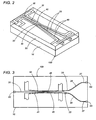
FIG. 2 is a perspective view of a major portion of the switch; -
FIG. 3 is a top view of the major portion of the switch including a core and heater elements; -
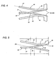
FIGS. 4 and 5 are enlarged top view illustrating the relation between the core and the heater elements; -
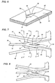
FIG. 6 is a partial perspective view illustrating a heat dissipater formed on a substrate of the switch; -
FIG. 7 is an enlarged top view illustrating a spatial relation of the heat dissipater with the heater elements and the core; -
FIG. 8 is an enlarged top view illustrating isothermal lines given by heating one of the heater elements; -
FIGS. 9 to 11 are sections of the switch respectively taken along line X-X, line Y-Y, and Z-Z ofFIG. 7 ; -
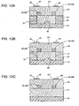
FIGS. 12A, 12B, and 12C are sectional views illustrating a thermal effect of the switch, respectively at one cross section; -
FIGS. 13A and 13B are graphs illustrating an advantageous effect of the switch; and -
FIG. 14 is a sectional view which is similar toFIG. 10 but illustrates another preferred embodiment of the present invention. - Referring now to
FIG. 1 , there is shown an optical switch in accordance with a preferred embodiment of the present invention. Theoptical switch 100 is adapted in use to be inserted in an optical fiber network for switching the light signal using the thermo-optic effect. Theswitch 100 is accommodated in arectangular base 110 together with aninput connector 120 for one inputoptical fiber 121 and anoutput connector 130 for twooptical fibers 131. Acover 140 is fitted on thebase 110 to conceal therebetween theswitch 100 and theconnectors FIG. 2 , theswitch 100 is shaped into a rectangular module of a layered structure including asubstrate 10 made of a silicon crystal, aclad layer 20, acore 30 embedded in the clad layer, and twoindependent heater elements 40 deposited on top of theclad layer 20. Theswitch 100 also includes a set ofelectrodes heater elements 40 to anexternal voltage source 200 to selectively heat one of theheater elements 40 to transmit light incoming though the inputoptical fiber 121 to one of the twooptical fibers 131. - The
clad layer 20 and thecore 30 are both made of a polymer such as polyimide. Thecore 30 is selected to give a refractive index greater than theclad layer 20 to give a refractive index difference (Δn) of 0.004 to 0.008, and is cooperative with theclad layer 20 to define a light guide for transmitting the light. - As shown in
FIGS. 9 to 11 , theclad layer 20 is composed of alower clad layer 21 and anupper clad layer 22 which are superimposed on theSi substrate 10 step-by-step, while thecore 30 is superimposed partially on thelower clad layer 21. The thickness of thelower clad layer 21 is selected to be between 7 µm to 20 µm as measured from the top of thesubstrate 10 to the bottom of thecore 30, while the thickness of theupper clad layer 22 is also between 7 µm to 20 µm as measured from the top of thecore 30. The thickness of theupper clad layer 22 where thecore 30 is not present is therefore increased by the thickness of thecore 30. - As shown in
FIGS. 2 and 3 , thecore 30 is shaped to have a generally square cross-section and extends horizontally within theclad layer 20 to form a Y-shape planar configuration with aninput line 31 and twooutput lines 33 branched off from theinput line 31 through anode 32. Thus, the width of thecore 30 is uniform expect at thenode 32, as best seen inFIG. 5 . The width of theinput line 31 and theoutput lines 33 is selected to be about 4 µm to 8 µm. Theinput line 31 extends straight from alight input terminal 91 which is connected to the inputoptical fiber 121 by means of theinput connector 120. Eachoutput line 33 includes astraight segment 35 that branches off from thenode 32, acurved segment 36 extending from thestraight segment 35, and a rearstraight segment 37 extending from the curved segment 60 and terminating at anoutput terminal 93, which is connected to each of the outputoptical fibers 131 at theoutput connector 130. Thecurved segment 36 is introduced for the purpose of reducing the overall length of theswitch 100. Thestraight segments 35 are branched off from thenode 32 at an angle of 0.1 ° to 0.2° and extend to a point where the two straight segments are spaced from each other at a distance 3 to 5 times the width of the core, i.e., 12 µm to 20 µm in case the core width is 4 µm. With this planar geometric of the core 30, the switch is given an improved isolation as much as 35 dB or more. When one of theheater elements 40 is energized, the adjacent one of theoutput lines 33 as well as a surrounding portion thereof are heated to lower their refractive indexes, whereby thecorresponding output line 33 becomes inactive while keeping theother output line 33 active to direct the light therethrough. - Referring to
FIGS. 4 and 5 , each of theheater elements 40 is shaped to have amain strip 45 partially overlapping with the end of thestraight segment 35 of the associated one of the output lines away from thenode 32 with regard to a horizontal projection plane in which theheater elements 40 and the core 30 project. Hereinafter, unless otherwise mentioned, the horizontal projection plane is relied upon to describe theheater element 40 in relation to thecore 30 and other parts. Themain strip 45 is mainly responsible for heating and therefore deactivating the adjacent one of the output lines 33. Themain strip 45 overlaps with thestraight segment 35 only at a portion of the straight segment outwardly of a center line thereof, thereby giving a sufficient gap to theother output line 33 to minimize the thermal effect on thestraight segment 35 of theactive output line 33. Upon one of theheater elements 40 being energized, thestraight segment 35 of theadjacent output line 33 as well as the surrounding portion of theclad layers output line 33 becomes inactive as a result of that the light intensity distribution LINT is greatly distorted or offset from the center of theoutput line 33, as indicted by dotted lines ofFIGS. 10 and 11 , which are cross sections corresponding to line Y-Y and Z-Z ofFIG. 7 , while theother output line 33 is kept free from critical thermal affection to direct the light therethrough in a regular pattern of the light intensity distribution LINT, the same as in theinput line 31, as shown inFIG. 9 . - Each
heater element 40 further includes adeflector strip 42 which is responsible for deflecting the light passing within thenode 32 towards the active one of thestraight segments 35 or the output lines 33. Thedeflector strip 42 extends continuously from themain strip 45 along a portion of thestraight segment 35 and thenode 32 while it is laterally spaced by a larger extent from the adjacentstraight segment 35 as it extends away from themain strip 45. In detail, thedeflector strip 42 runs generally in parallel with an extension line EX of the non-associatedstraight segment 35, as best shown inFIG. 5 , to heat only the adjacent side of thenode 32 to deflect the light into thestraight segment 35 of theactive output line 33, while avoiding thatstraight segment 35 from being thermally affected to a critical extent. Further, theheater element 40 is additionally formed with anintroductory strip 41 which extends continuously from thedeflector strip 42 to run along a portion of theinput line 31. Theintroductory strip 41 is provided to heat the adjacent side or the width part of theinput line 31 to some extent in order to offset the light passing through theinput line 31 towards the non-adjacent side thereof leading through thenode 32 to thestraight segment 35 of theactive output line 33, thereby effectively guiding the light from theinput line 31 past thenode 32 to theactive output line 33 with improved isolation. Theintroductory strip 41 extends continuously along the same axis of thedeflector strip 42 in an inclined relation with respect to theinput line 31 so as to come closer to the input line as it advances to thedeflector strip 42. - Referring to
FIGS. 6 to 10 , aheat dissipater 50 is formed at the interface between thesubstrate 10 and the lowerclad layer 21 to absorb the heat given off from one of theheater elements 40 for protecting the core 30 from being adversely affected by the heat. Theheat dissipater 50 is fabricated integrally with theSi substrate 10 to project into the lowerclad layer 21, and has a thermal conductivity higher than theclad layers heat dissipater 50, the heat given off from one of theheater elements 40 and conducting past theadjacent output line 33 can be well absorbed by theheat dissipater 50, as indicated by isothermal lines IST ofFIG. 12A , to thereby protect theother output line 33 from being thermally affected critically. This is true even if a large amount of heat is applied in an attempt to improve the isolation, i.e., to minimize the light radiation out from the active output line and maximize the light transmission therethrough. In this case, corresponding isothermal lines IST becomes tense, as shown inFIG. 12B , so that theactive output line 33 can be kept from being thermally affected even by the increased amount of the heat. Otherwise, theactive output line 33 would be thermally affected to increase the insertion loss, as shown inFIG. 12C . - Turning back to
FIGS. 6 and 7 , theheat dissipater 50 is kite-shaped in a planer configuration to have a front smalltriangular section 51 and a rear largetriangular section 52 within the horizontal projection plane, and is arranged immediately downwardly of thenode 32 to overlap the same as well as the adjacent portions of the core 30 with the front smalltriangular section 51 disposed on the side of theinput line 31, as best shown inFIG. 6 . The reartriangular section 52 has twoadjacent sides 56 which run parallel to theadjacent deflector strip 42 and merges into arear vertex 57 in registration with an axis of theinput line 31. Since theadjacent sides 56 is generally in parallel with theadjacent deflector strip 42, the isothermal lines IST (indicated by dotted lines inFIG. 8 ) developed by heating one of theheater elements 30 also runs parallel to thestraight segment 35 of theactive output line 33 so that the above effect of protecting theactive output line 33 from being thermally affected can be optimized, thereby improving the isolation as well as reducing the insertion loss of the switch. In this connection, the top faces of the reartriangular sections 52 are each inclined to be directed the adjacentstraight segment 35, as seen inFIGS. 10 and 11 , to give a temperature gradient along that direction so as to distort the light in theinactive output line 33 not to interfere with the light propagating through theactive output line 33 for improved isolation of the light. - The front small
triangular section 51 is provided to define an introductory heat dissipater for successfully directing the light from theinput line 31 to theactive output line 33 past thenode 32. Theintroductory heat dissipater 51 is disposed at a portion downwardly of theinput line 31 immediately below thenode 32 in order to expedite thermal transfer of heat conducting towards theinput line 31, thereby heating only the adjacent side of theinput line 31 and therefore keeping the opposite adjacent side free from being thermally affected for effectively offsetting the light proceeding into thenode 32 and subsequently into theactive output line 33. - As shown in
FIGS. 10 and 11 , the switch includes a pair of bottom cladlayers 24 which are disposed adjacent to thesubstrate 10 and have a refractive index lower than the lowerclad layer 21. The bottom cladlayers 24 are laterally spaced from each other and offset laterally outwardly of theadjacent output lines 33 with respect to the horizontal projection plane. The bottom cladlayers 24 are introduced to minimize the thermal effect on theactive output line 33 when the other output line is heated to become inactive, for optimum light transmission efficiency through theactive output line 33. For this purpose, the bottom cladlayer 24 is located on an extension line connecting one of theheater elements 40 and the non-associated one of theoutput lines 33 to give a refractive index gradient along that line, as shown inFIG. 13A , in which relatively thin lines indicate the refractive index (n) when the active output line is not heated, while relatively thick lines indicate the refractive index (n) when the active output line is heated. Also in the figure, effective refractive index of the core is indicated by dotted lines. With this arrangement of giving a lowered refractive index to a portion, i.e., the bottom cladlayer 24 which is remote from the source of heat and is therefore subject to less lowering of the refractive index than the upper cladlayer 22, theactive output line 33 can be surrounded entirely by the portion having the lowered refractive index than that of theoutput line 33. Whereby, theactive output line 33 can be given its maximum efficiency for transmitting the light to minimize the radiation loss. Otherwise, i.e. without the bottom clad layer of lowered refractive index, the lowerclad layer 21 may be given at its bottom a region having the refractive index still greater than that of the active output line, as indicated by R inFIG. 13B , which induces a certain radiation loss and detracts from the optimum light transmitting efficiency. In order to take the advantages of the above effect, each of the bottom cladlayers 24 are preferred to have its top adjacent to the top of thecore 30. However, the bottom cladlayer 24 may have its top lower than the bottom of the core 30, as shown inFIGS. 11 and12 . -
FIG. 14 illustrates the present invention which is basically identical with the above embodiment except that aflat heat dissipater 50A is fabricated as an integral part of theSi substrate 10A. Uke parts are designated by like reference numerals with a suffix letter of "A". In this embodiment, theheat dissipater 50A is formed to remain integral with theSi substrate 10A by oxidizing theperipheral portion 90 into SiO2.
Claims (5)
- An optical switch comprising:a substrate (10; 10A) having a length and width;a clad layer (20) formed on said substrate and having a negative thermo-optic coefficient (dn/dT);a core (30) embedded within said clad layer to be surrounded thereby,said core extending horizontally generally along the length of said substrate,said core being made of a transparent material having a negative thermo-optic coefficient (dn/dT), said core having a refractive index different from a refractive index of the surrounding clad layer to give a difference between these refractive indexes so as to constitute a light guide with the surrounding clad layer for transmitting the light, said core including an input line (31) leading from a light input terminal (91) to a node (32), two output lines (33) branching off from said node and leading to individual light output terminals (93),two heater elements (40) each disposed adjacent to each of said two output lines to extend horizontally generally along the length of said substrate, said heater elements being adapted to be connected to a voltage source for selectively heating one of said output lines to lower the refractive index thereof to such an extent as to make the selected output line inactive,said two output lines of the core including individual straight segments (35) that branch off from said node (32),each of said heater elements (40) including a main strip (45) overlapping at least partially with said straight segment (35) of the adjacent output line (33) with respect to a horizontal projection plane on which the heater elements and the core project, and a deflector strip (42) extending from said main strip (45) along said node (32) with respect to said horizontal projection plane, wherein each of said deflector strips (42) runs in a spaced relation with said node (32) and in a generally parallel relation with an extension line of the straight segment (35) of the non-associated output line (33) with respect to said horizontal projection plane,a heat dissipater (50; 50A) being disposed at the interface between said clad layer (20) and said substrate (10),said heat dissipater (50; 50A) having a thermal conductivity higher than said clad layer in order to expedite thermal transfer of heat from each one of said heater elements to said substrate for protecting the non-heated one of said output lines from being thermally affected,characterized in thatsaid heat dissipater (50) is formed integrally with said substrate to project into the clad layer at a portion between said straight segments (35) of the two output lines with respect to the horizontal projection plane.
- The optical switch as set forth in claim 1, further including:an introductory heat dissipater (51) which is disposed at the interface between said clad layer and said substrate, and formed integrally with said substrate to project into the clad layer at a portion downwardly of said input line (31),said introductory heat dissipater having a thermal conductivity higher than said clad layer in order to expedite thermal transfer of heat conducting through said input line to said substrate.
- The optical switch as set forth in claim 1, wherein
said heat dissipater (50) includes, within said horizontal projection plane, a triangular section (52) with two adjacent sides (56) forming a vertex (57) therebetween, said triangular section being disposed to overlap with said straight segments (35) adjacent to said node (32) with said vertex directed away from said node and with said two adjacent sides (56) generally in parallel relation respectively with said deflector strips (42) of said heater elements (40) with respect to said horizontal projection plane. - The optical switch as set forth in claim 1, wherein
said clad layer (20) is composed of a lower clad layer (21) and an upper clad layer (22) which are superimposed on the substrate (10) step-by-step, and that
a pair of bottom clad layers (24) are disposed in said lower clad layer (21) between said upper clad layer (22) and said substrate (10),
said bottom layers being laterally spaced from each other and offset laterally outwardly of the adjacent output lines (33) with respect to the horizontal projection plane,
said bottom clad layer (24) having a refractive index lower than said clad layer. - The optical switch as set forth in claim 4, wherein
each of said bottom clad layers (24) has its top lower than the top of said output lines of said core.
Applications Claiming Priority (1)
| Application Number | Priority Date | Filing Date | Title |
|---|---|---|---|
| PCT/JP2004/013019 WO2006025116A1 (en) | 2004-09-01 | 2004-09-01 | Optical switch |
Publications (2)
| Publication Number | Publication Date |
|---|---|
| EP1787163A1 EP1787163A1 (en) | 2007-05-23 |
| EP1787163B1 true EP1787163B1 (en) | 2010-11-24 |
Family
ID=34958783
Family Applications (1)
| Application Number | Title | Priority Date | Filing Date |
|---|---|---|---|
| EP04772891A Expired - Lifetime EP1787163B1 (en) | 2004-09-01 | 2004-09-01 | Optical switch |
Country Status (4)
| Country | Link |
|---|---|
| EP (1) | EP1787163B1 (en) |
| JP (1) | JP4997481B2 (en) |
| DE (1) | DE602004030285D1 (en) |
| WO (1) | WO2006025116A1 (en) |
Cited By (1)
| Publication number | Priority date | Publication date | Assignee | Title |
|---|---|---|---|---|
| EP3441817A4 (en) * | 2016-05-04 | 2019-07-10 | Huawei Technologies Co., Ltd. | OPTICAL SWITCH |
Families Citing this family (1)
| Publication number | Priority date | Publication date | Assignee | Title |
|---|---|---|---|---|
| JP5950937B2 (en) | 2011-01-21 | 2016-07-13 | フラウンホーファー−ゲゼルシャフト・ツール・フェルデルング・デル・アンゲヴァンテン・フォルシュング・アインゲトラーゲネル・フェライン | Polymerizable composition, cured product obtained therewith and use of these materials |
Family Cites Families (9)
| Publication number | Priority date | Publication date | Assignee | Title |
|---|---|---|---|---|
| JP3204493B2 (en) * | 1996-01-31 | 2001-09-04 | 日本電信電話株式会社 | Manufacturing method of optical waveguide with phase adjustment function |
| JP3868122B2 (en) * | 1998-08-12 | 2007-01-17 | 日本電信電話株式会社 | Thermo-optic light modulator |
| JP2000258736A (en) * | 1999-03-09 | 2000-09-22 | Oki Electric Ind Co Ltd | Quartz-base optical switch |
| US6741775B2 (en) * | 2000-02-04 | 2004-05-25 | Fujikura Ltd. | Optical switch |
| JP2003005232A (en) * | 2001-04-18 | 2003-01-08 | Ngk Insulators Ltd | Optical device |
| KR100390330B1 (en) * | 2001-08-17 | 2003-07-04 | 한국전자통신연구원 | Optical switching device |
| JP2004085744A (en) * | 2002-08-26 | 2004-03-18 | Matsushita Electric Works Ltd | Optical switch and method for manufacturing the same |
| JP2005156825A (en) * | 2003-11-25 | 2005-06-16 | Matsushita Electric Works Ltd | Optical attenuator |
| JP2006047604A (en) * | 2004-08-04 | 2006-02-16 | Nippon Telegr & Teleph Corp <Ntt> | Glass deposition substrate, and thermooptic modulator, and method for manufacturing them |
-
2004
- 2004-09-01 DE DE602004030285T patent/DE602004030285D1/en not_active Expired - Lifetime
- 2004-09-01 JP JP2007509802A patent/JP4997481B2/en not_active Expired - Fee Related
- 2004-09-01 EP EP04772891A patent/EP1787163B1/en not_active Expired - Lifetime
- 2004-09-01 WO PCT/JP2004/013019 patent/WO2006025116A1/en not_active Ceased
Cited By (2)
| Publication number | Priority date | Publication date | Assignee | Title |
|---|---|---|---|---|
| EP3441817A4 (en) * | 2016-05-04 | 2019-07-10 | Huawei Technologies Co., Ltd. | OPTICAL SWITCH |
| US10481466B2 (en) | 2016-05-04 | 2019-11-19 | Huawei Technolgies Co., Ltd. | Optical switch |
Also Published As
| Publication number | Publication date |
|---|---|
| JP2008511013A (en) | 2008-04-10 |
| WO2006025116A1 (en) | 2006-03-09 |
| EP1787163A1 (en) | 2007-05-23 |
| JP4997481B2 (en) | 2012-08-08 |
| DE602004030285D1 (en) | 2011-01-05 |
Similar Documents
| Publication | Publication Date | Title |
|---|---|---|
| US10345629B2 (en) | Planar optical phase shifters with efficient heater placement | |
| US6282335B1 (en) | Thermo-optical switch | |
| Lai et al. | Low-power compact 2× 2 thermooptic silica-on-silicon waveguide switch with fast response | |
| EP2741122B1 (en) | Thermal tuning of an optical device | |
| CN1192277C (en) | Method and apparatus for stable control of electrooptic devices | |
| JP2010517113A (en) | Thermo-optic waveguide device | |
| US11709382B2 (en) | High-efficiency thermal phase shifter | |
| US5623566A (en) | Network with thermally induced waveguide | |
| US4737002A (en) | Tunable optical directional couplers | |
| KR100326046B1 (en) | Thermo-optic switch and method of forming the same | |
| US4648687A (en) | Optical switching device | |
| EP3441817B1 (en) | Optical switch | |
| WO2006025116A1 (en) | Optical switch | |
| CN103558657A (en) | Array waveguide grating | |
| EP1293823B1 (en) | Optical switch comprising two non-coplanar arrays of optical waveguides | |
| JP4519248B2 (en) | Optical device with optical waveguide | |
| US6741775B2 (en) | Optical switch | |
| JP2003075788A (en) | Optical device | |
| WO2021132953A1 (en) | Light source using photonic crystal structure | |
| JP3534385B2 (en) | Thermo-optic switch | |
| JP3920730B2 (en) | Thermo-optic light switch | |
| US6961493B2 (en) | Optical device | |
| JP4534607B2 (en) | Waveguide-type variable optical attenuator | |
| KR100416967B1 (en) | Planer lightwave circuit module with heat transfer device | |
| JP2001166345A (en) | Thermo-optic switch array |
Legal Events
| Date | Code | Title | Description |
|---|---|---|---|
| PUAI | Public reference made under article 153(3) epc to a published international application that has entered the european phase |
Free format text: ORIGINAL CODE: 0009012 |
|
| 17P | Request for examination filed |
Effective date: 20070301 |
|
| AK | Designated contracting states |
Kind code of ref document: A1 Designated state(s): DE |
|
| DAX | Request for extension of the european patent (deleted) | ||
| RBV | Designated contracting states (corrected) |
Designated state(s): DE |
|
| 17Q | First examination report despatched |
Effective date: 20081017 |
|
| RAP1 | Party data changed (applicant data changed or rights of an application transferred) |
Owner name: FRAUNHOFER-GESELLSCHAFT ZUR FOERDERUNG DER ANGEWAN Owner name: PANASONIC ELECTRIC WORKS CO., LTD. |
|
| GRAP | Despatch of communication of intention to grant a patent |
Free format text: ORIGINAL CODE: EPIDOSNIGR1 |
|
| GRAS | Grant fee paid |
Free format text: ORIGINAL CODE: EPIDOSNIGR3 |
|
| GRAA | (expected) grant |
Free format text: ORIGINAL CODE: 0009210 |
|
| AK | Designated contracting states |
Kind code of ref document: B1 Designated state(s): DE |
|
| REF | Corresponds to: |
Ref document number: 602004030285 Country of ref document: DE Date of ref document: 20110105 Kind code of ref document: P |
|
| RIN2 | Information on inventor provided after grant (corrected) |
Inventor name: MIYAGAWA, NOBUYUKI Inventor name: DANNBERG, PETER Inventor name: WAECHTER, CHRISTOPH Inventor name: UCHIDA, YUICHI |
|
| PLBE | No opposition filed within time limit |
Free format text: ORIGINAL CODE: 0009261 |
|
| STAA | Information on the status of an ep patent application or granted ep patent |
Free format text: STATUS: NO OPPOSITION FILED WITHIN TIME LIMIT |
|
| 26N | No opposition filed |
Effective date: 20110825 |
|
| REG | Reference to a national code |
Ref country code: DE Ref legal event code: R097 Ref document number: 602004030285 Country of ref document: DE Effective date: 20110825 |
|
| PGFP | Annual fee paid to national office [announced via postgrant information from national office to epo] |
Ref country code: DE Payment date: 20150922 Year of fee payment: 12 |
|
| REG | Reference to a national code |
Ref country code: DE Ref legal event code: R119 Ref document number: 602004030285 Country of ref document: DE |
|
| PG25 | Lapsed in a contracting state [announced via postgrant information from national office to epo] |
Ref country code: DE Free format text: LAPSE BECAUSE OF NON-PAYMENT OF DUE FEES Effective date: 20170401 |