EP1786039A2 - Flat Panel Display Device - Google Patents
Flat Panel Display Device Download PDFInfo
- Publication number
- EP1786039A2 EP1786039A2 EP06123684A EP06123684A EP1786039A2 EP 1786039 A2 EP1786039 A2 EP 1786039A2 EP 06123684 A EP06123684 A EP 06123684A EP 06123684 A EP06123684 A EP 06123684A EP 1786039 A2 EP1786039 A2 EP 1786039A2
- Authority
- EP
- European Patent Office
- Prior art keywords
- power bus
- bus line
- metal layer
- line
- electrode
- Prior art date
- Legal status (The legal status is an assumption and is not a legal conclusion. Google has not performed a legal analysis and makes no representation as to the accuracy of the status listed.)
- Granted
Links
Images

Classifications
-
- H—ELECTRICITY
- H05—ELECTRIC TECHNIQUES NOT OTHERWISE PROVIDED FOR
- H05B—ELECTRIC HEATING; ELECTRIC LIGHT SOURCES NOT OTHERWISE PROVIDED FOR; CIRCUIT ARRANGEMENTS FOR ELECTRIC LIGHT SOURCES, IN GENERAL
- H05B33/00—Electroluminescent light sources
- H05B33/10—Apparatus or processes specially adapted to the manufacture of electroluminescent light sources
-
- H—ELECTRICITY
- H10—SEMICONDUCTOR DEVICES; ELECTRIC SOLID-STATE DEVICES NOT OTHERWISE PROVIDED FOR
- H10K—ORGANIC ELECTRIC SOLID-STATE DEVICES
- H10K59/00—Integrated devices, or assemblies of multiple devices, comprising at least one organic light-emitting element covered by group H10K50/00
- H10K59/10—OLED displays
- H10K59/12—Active-matrix OLED [AMOLED] displays
- H10K59/131—Interconnections, e.g. wiring lines or terminals
- H10K59/1315—Interconnections, e.g. wiring lines or terminals comprising structures specially adapted for lowering the resistance
-
- H—ELECTRICITY
- H05—ELECTRIC TECHNIQUES NOT OTHERWISE PROVIDED FOR
- H05B—ELECTRIC HEATING; ELECTRIC LIGHT SOURCES NOT OTHERWISE PROVIDED FOR; CIRCUIT ARRANGEMENTS FOR ELECTRIC LIGHT SOURCES, IN GENERAL
- H05B33/00—Electroluminescent light sources
- H05B33/12—Light sources with substantially two-dimensional [2D] radiating surfaces
- H05B33/26—Light sources with substantially two-dimensional [2D] radiating surfaces characterised by the composition or arrangement of the conductive material used as an electrode
-
- H—ELECTRICITY
- H10—SEMICONDUCTOR DEVICES; ELECTRIC SOLID-STATE DEVICES NOT OTHERWISE PROVIDED FOR
- H10K—ORGANIC ELECTRIC SOLID-STATE DEVICES
- H10K59/00—Integrated devices, or assemblies of multiple devices, comprising at least one organic light-emitting element covered by group H10K50/00
- H10K59/10—OLED displays
- H10K59/12—Active-matrix OLED [AMOLED] displays
-
- H—ELECTRICITY
- H10—SEMICONDUCTOR DEVICES; ELECTRIC SOLID-STATE DEVICES NOT OTHERWISE PROVIDED FOR
- H10K—ORGANIC ELECTRIC SOLID-STATE DEVICES
- H10K59/00—Integrated devices, or assemblies of multiple devices, comprising at least one organic light-emitting element covered by group H10K50/00
- H10K59/10—OLED displays
- H10K59/12—Active-matrix OLED [AMOLED] displays
- H10K59/131—Interconnections, e.g. wiring lines or terminals
-
- H—ELECTRICITY
- H10—SEMICONDUCTOR DEVICES; ELECTRIC SOLID-STATE DEVICES NOT OTHERWISE PROVIDED FOR
- H10K—ORGANIC ELECTRIC SOLID-STATE DEVICES
- H10K59/00—Integrated devices, or assemblies of multiple devices, comprising at least one organic light-emitting element covered by group H10K50/00
- H10K59/10—OLED displays
- H10K59/12—Active-matrix OLED [AMOLED] displays
- H10K59/121—Active-matrix OLED [AMOLED] displays characterised by the geometry or disposition of pixel elements
- H10K59/1213—Active-matrix OLED [AMOLED] displays characterised by the geometry or disposition of pixel elements the pixel elements being TFTs
Definitions
- the present invention relates to a flat panel display device, and more particularly, to an organic light emitting display device with reduced unused image area because of a panel identification mark, and with low resistance power bus lines.
- a panel identification mark is included in a flat panel display device such as a liquid crystal display device, an organic light emitting display device, or an inorganic light emitting display device, to allow convenient identification, tracking of the panel, and evaluation of the display cells.
- the panel identification mark is located on a separate area outside the display region where images are displayed. Therefore, the space occupied by the panel identification mark is unused space, where images are not displayed, and the unused space increases in area as the size of the panel identification mark increases.
- the panel identification mark is usually located in existing unused space, for instance under a driving chip, where it does not affect other signals and does not need additional area.
- the liquid crystal display device in the conventional art does not supply additional power to each of the pixels.
- a power supply line for supplying power to each pixel must be extended. Accordingly, the unused area in the panel is further increased. Therefore, it is difficult to lay out the panel identification mark without increasing the unused area of the panel.
- An organic light emitting display device that reduces unused area and reduces a drive voltage drop is disclosed.
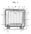
- FIG. 1 is a plan view of an active matrix (AM) organic light emitting display device according to an embodiment.
- AM active matrix
- a display region 2 where images are displayed is formed on a substrate 31.
- the display region 2 is sealed by an additional sealing member (not shown) to protect the display region 2 from impact, moisture, and air.
- the sealing member may be, for example, an insulating substrate or a metal cap.
- a terminal region 1 comprising terminals is located on an end portion of the substrate 31 where the display region 2 is formed. The terminal region 1 is exposed outside the sealing member.
- a driving power bus line 21 for supplying driving power to a Vdd line 20
- an electrode power bus line 22 connected to a facing electrode 53 to supply facing electrode power
- various circuits 23 and 24 that control signals applied to the display region 2.
- Areas where the terminal region 1, the driving power bus line 21, the electrode power bus line 22, and the circuits 23 and 24 are located correspond to an unused area where images are not displayed.
- the driving power bus line 21 is formed to surround the entire display region 2 from an end of a driving power terminal unit 11 to the other end of the driving power terminal unit 11, and also, is disposed in a lower side of the display region 2 by being connected through driving power lines Vdd 20 that cross the display region 2.
- the electrode power bus line 22 which is electrically connected to an electrode of the organic light emitting display device in the display region 2 and will be described in detail later, is formed on a side of the display region 2.
- the electrode connected to the electrode power bus line 22 can be extended to cover the electrode power bus line 22.
- An insulating film is interposed between the electrode connected to the electrode power bus line 22 and the electrode power bus line 22, and the electrode and the electrode power bus line 22 are connected through a plurality of contact holes 25.
- the vertical circuit unit 23 and the horizontal circuit unit 24 are mounted between the driving power bus line 21 and the display region 2.
- the vertical circuit unit 23 can be a scan driving circuit unit that applies scan signals to gate lines of the display region 2, and is electrically connected to a scan terminal unit 13 in the terminal region 1.
- the horizontal circuit unit 24 can be a data driving circuit unit that applies data signals to data lines of the display region 2, and is electrically connected to a data terminal unit 14 in the terminal region 1.
- the vertical circuit unit 23 and the horizontal circuit unit 24 can be formed on the substrate 31 using a patterning method, or can include an external IC or COG.
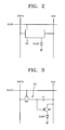
- the display region 2 includes a plurality of pixels, each of which can have a pixel circuit as depicted in FIG. 2.
- each pixel includes a data line Data, a scan line Scan, and a power supply line Vdd that supplies driving power to an organic light emitting diode (OLED).
- the supply line Vdd corresponds to a driving power line Vdd 20 of FIG. 1.
- the pixel circuit PC of each pixel is electrically connected to the data line, the scan line Scan, and the supply line Vdd, and controls the light emission of the OLED.
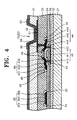
- FIG. 3 is a detailed schematic diagram of the unit pixel of FIG. 2.
- the pixel circuit PC of each pixel includes two thin film transistors M1 and M2 and one capacitor unit Cst.
- each pixel of the organic light emitting display device includes at least two thin film transistors (TFTs), i.e. a switching TFT M2 and a driving TFT M1, a capacitor unit Cst, and an OLED.
- TFTs thin film transistors
- the switching TFT M2 is turned on or off by a scan signal applied to a scan line Scan to transmit a data signal applied to the data line Data to the storage capacitor unit Cst and the driving TFT M1.
- the switching device is not limited to the switching TFT M2 depicted in FIG. 4, and can be a switching circuit having a plurality of TFTs and capacitors, or can further include a circuit that compensates for a threshold voltage Vth value of the driving TFT M1 or a circuit that compensates for a voltage drop of the Vdd power line Vdd.
- the driving TFT M1 determines the current input to the OLED according to a data signal transmitted through the switching TFT M2.
- the capacitor unit Cst stores the data signal transmitted from the switching TFT M2 for one frame period.
- the driving TFT M1 and the switching TFT M2 are depicted as PMOS TFTs, but other transistors may also be used.
- One or both of the driving TFT M1 and the switching TFT M2 can be an NMOS TFT.
- the number of TFTs and capacitors is not limited to that shown in FIG. 3, and can be increased as necessary.
- the pixel circuit PC has a cross-sectional structure as depicted in FIG. 4.
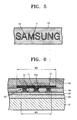
- FIG. 4 is a cross-sectional view of a portion of the pixel of FIG. 3. Referring to FIG. 4, a TFT 40 and an OLED are included on a substrate 31.
- the substrate 31 can be formed of acryl, polyimide, polycarbonate, polyester, mylar, or a plastic material, but embodiments are not limited to these materials, and the substrate 31 can be formed of a metal foil such as SUS, tungsten, etc., glass or another material or combination of materials.
- a barrier layer and/or a buffer layer can be formed on the upper surface of the substrate 31 to prevent the diffusion of impurity ions, prevent the penetration of moisture or external air, and/or planarize the surface.
- An active layer 41 of the TFT 40 is formed on the insulating layer 32 using a semiconductor material, and a gate insulating film 33 is formed to cover the active layer 41.
- the active layer 41 can be formed of an inorganic semiconductor material such as amorphous silicon, polysilicon, or an organic semiconductor material.
- the active layer 41 includes a channel region 411 between a source region 412 and a drain region 413.
- a gate electrode 42 is formed on the gate insulating film 33, and an interlayer insulating film 34 covering the gate electrode 42 is formed.
- a source electrode 43 and a drain electrode 44 are formed on the interlayer insulating film 34.
- a passivation film 35 and a pixel defining film 37 are sequentially formed to cover the source electrode 43 and the drain electrode 44.
- the gate insulating film 33, the interlayer insulating film 34, the passivation film 35, and the pixel defining film 37 can each have a single layer structure or a multi-layer structure, and can be formed of an organic material, an inorganic material, or a composite of organic and inorganic materials.
- the stacking structure of a TFT according to these embodiments is not limited to that of the TFT 40, and various TFT structures can be used.
- a pixel electrode 51 which is an electrode of the OLED, is formed on the passivation film 35, and a pixel defining film 37 is formed on the pixel electrode 51. After exposing the pixel electrode 51 through a predetermined opening 38 in the pixel defining film 37, an organic light emitting film 52 of the OLED is formed.
- the OLED emits red, green, or blue light according to the current supplied to form a predetermined image, and comprises the pixel electrode 51 that contacts the drain electrode 44 of the TFT 40 through a contact hole 36, a facing electrode 53 covering all of the pixels, and the organic light emitting film 52, which is located between the pixel electrode 51 and the facing electrode 53 and emits light.
- the pixel electrode 51 and the facing electrode 53 are insulated from each other by the organic light emitting film 52, and apply voltages of opposite polarity to the organic light emitting film 52 so that the organic light emitting film 52 emits light.
- the organic light emitting film 52 can be, for example, a small molecular weight organic film or a polymer organic film. If the organic light emitting film 52 is a small molecular weight organic film, the organic light emitting film 52 can include a hole injection Layer (HIL), a hole transport layer (HTL), an emission layer (EML), an electron transport layer (ETL), or an electron injection layer (EIL), can be stacked in a single structure or a composite structure, and can be composed of copper phthalocyanine (CuPc), N,N'-di(naphthalene-1-yl)-N,N'-diphenyl-benzidine (NPB), or tris-8-hydroxyquinoline aluminum (Alq3).
- HIL hole injection Layer
- HTL hole transport layer
- EML emission layer
- ETL electron transport layer
- EIL electron injection layer
- CuPc copper phthalocyanine
- NPB N,N'-di(naphthalene-1-yl)-N,N'-
- the small molecular weight organic film can be formed using a vacuum evaporation method.
- the HIL, the HTL, the ETL, and the EIL are common electrodes, and can be commonly formed in red, green, and blue pixels. Accordingly, the common electrodes can cover the pixels like the facing electrode 53.
- the organic light emitting film 52 can include a HTL and an EML.
- the HTL can be formed of PEDOT
- the EML can be formed of poly-phenylenevinylene (PPV) and polyfluorene.
- the polymer organic film can be formed by screen printing, ink jet printing, etc.
- the organic light emitting film 52 is not limited to the configuration described above, and can take various forms.
- the pixel electrode 51 functions as an anode electrode
- the facing electrode 52 functions as a cathode electrode.
- the polarity of the pixel electrode 51 and the facing electrode 53 may be reversed.
- the pixel electrode 51 can be a transparent electrode, and the facing electrode 53 can be a reflective electrode.
- the pixel electrode 51 can comprise a transparent material having a high work function, such as, but not limited to ITO, IZO, In 2 O 3 , or ZnO, and the facing electrode 53 can comprise a reflective metal having a low work function, such as, but not limited to Ag, Mg, Al, Pt, Pd, Au, Ni, Nd, Ir, Cr, Li, Ca, or a compound of these metals.
- the pixel electrode 51 can be a reflective electrode, and the facing electrode 53 can be a transparent electrode.
- the pixel electrode 51 can be formed of a material having a high work function such as, but not limited to, ITO, IZO, In 2 O 3 , or ZnO after forming a reflective film using Ag, Mg, Al, Pt, Pd, Au, Ni, Nd, Ir, Cr, Li, Ca, or a compound of these metals.
- the facing electrode 53 can include a material layer comprising a metal having a low work function, such as, but not limited to, Li, Ca, LiF/Ca, LiF/Al, Al, Ag, Mg, or a compound of these metals, and an auxiliary electrode layer or a bus electrode line comprising a transparent conductive material, such as, but not limited to, ITO, IZO, ZnO or In 2 O 3 , formed on the material layer.
- a metal having a low work function such as, but not limited to, Li, Ca, LiF/Ca, LiF/Al, Al, Ag, Mg, or a compound of these metals
- an auxiliary electrode layer or a bus electrode line comprising a transparent conductive material, such as, but not limited to, ITO, IZO, ZnO or In 2 O 3 , formed on the material layer.
- both the pixel electrode 51 and the facing electrode 53 can be transparent electrodes.
- the materials for forming the pixel electrode 51 and the facing electrode 53 are not limited to the materials described above.
- the pixel electrode 51 and the facing electrode 53 can be formed of a conductive paste containing a conductive organic material or conductive particles of Ag, Mg, Cu, etc.
- the paste can be printed by inkjet printing and annealed to form an electrode.
- the upper part of the OLED is sealed to substantially prevent exposure to the atmosphere.
- the gate electrode 42, the source electrode 43, and the drain electrode 44 can comprise a metal such as Ag, Mg, Al, Pt, Pd, Au, Ni, Nd, Ir, Cr, Li, Ca, a compound of these metals, or a transparent conductive material, such as ITO, IZO, ZnO or In 2 O 3 as the conductor described above.
- the gate electrode 42, the source electrode 43, and the drain electrode 44 can comprise a conductive paste containing a conductive organic material or conductive particles of Ag, Mg, Cu, etc. In the OLED according to the embodiment illustrated in FIG.
- the gate electrode 42 has a single layer structure, the source electrode 43 and the drain electrode 44 have a three-layer structure, but embodiments are not limited to these structures.
- the gate electrode 42 can also have a three-layer structure.
- the description will focus mainly on embodiments in which the gate electrode 42 has a single layer structure and the source electrode 43 and the drain electrode 44 have a three-layer structure as depicted in FIG. 5.
- the source electrode 43 can have a stacked structure including first, second and third conductive layers 431, 432 and 433, and the drain electrode 44 can have a stacked structure including first, second, and third conductive layers 441, 442, and 443.
- the second conductive layers 432 and 442 can be formed of aluminum or an aluminum alloy, such as Al, AlSi, AlNd, or AlCu.
- At least one of the first conductive layers 431 and 441 and the third conductive layers 433 and 443 can be formed of at least one material selected from Cr, Cr alloy, Mo, Mo alloy, W, and W alloy.
- the first conductive layers 431 and 441 and the third conductive layers 433 and 443 can comprise molybdenum tungsten (MoW) alloy, and the second conductive layers 432 and 442 can be formed of AlNd alloy.
- MoW molybdenum tungsten
- At least one of the first conductive layers 431 and 441 and the third conductive layers 433 and 443 can comprise at least one material selected from Ti, a Ti alloy, Ta, and a Ta alloy.
- the first conductive layers 431 and 441 and the third conductive layers 433 and 443 can comprise Ti
- the second conductive layers 432 and 442 can comprise an aluminum group metal
- the conductive layers are not limited thereto, and a layer structure can further be included in addition to the three layer structure.
- a cladding unit 45 can be formed of an insulating material to cap the side of the source electrode 43 and the drain electrode 44.
- the organic material can comprise a polymer derivative having a phenol group, an acryl group polymer, an imide group polymer, an arylether group polymer, an amide group polymer, a fluorine group polymer, a p-xylyrene group polymer, a vinyl alcohol group polymer, and a composition of more than one of these materials.
- the passivation film 35 can be formed of an acryl material, for example, a photosensitive acryl material that can be easily patterned.
- the inorganic material can comprise at least one of SiO 2 , SiN x , SiON, Al 2 O 3 , TiO 2 , Ta 2 O 5 , HfO 2 , ZrO 2 , Barium Strontium Titanate (BST), and PZT.
- the source electrode 43 and the drain electrode 44 have a multilayer structure, the overall conductivity of the source electrode 43 and the drain electrode 44 can be improved.
- the second conductive layers 432 and 442 are formed of an aluminum group metal having high conductivity.
- the second conductive layers 432 and 442 are protected by the first conductive layers 431 and 441 and the third conductive layers 433 and 443.
- the multilayer structure may also be used for electrically operative lines other than power lines, such as signal lines, control lines, and shielding lines.
- the cladding unit 45 can prevent the second conductive layers 432 and 442 formed of an aluminum group metal from being corroded or etched due to the penetration of an etchant through the side surfaces of the source electrode 43 and the drain electrode 44.
- the cladding unit 45 is particularly useful for protecting the source electrode 43 and the drain electrode 44 from the penetration of an etchant when the pixel electrode 51 is patterned.
- the cladding may also be used for electrically operative lines other than power lines, such as signal lines, control lines, and shielding lines.
- a Vdd line 20 can also be formed when the source electrode 43 and the drain electrode 44 are formed.
- the Vdd line formed at the same time as the source electrode 43 and the drain electrode 44 also has a first conductive layer 201, a second conductive layer 202, and a third conductive layer 203.
- the first conductive layer 201, the second conductive layer 202, and the third conductive layer 203 can be formed of the same materials described above.
- a cladding unit 25 can also be formed in the Vdd line 20 as described above.
- the function of the cladding unit 25 is the same as that of the cladding unit 45, thus a detailed description thereof will be omitted.
- a plurality of conductors can be formed in addition to the Vdd line 20 in the pixel.
- the driving power bus line 21 and the electrode power bus line 22 shown in FIG. 1 can be formed at the same time.
- a metal layer 70 overlaps the driving power bus line 21 and connects electrically to the driving power bus line 21.
- the metal layer 70 can be formed, for example, adjacent to the driving power bus line 21 and have a length substantially corresponding to the driving power bus line 21.
- the metal layer 70 may be long enough to reduce the voltage drop of the driving power bus line 21, which will be described later.
- the metal layer 70 can be formed at the same time as the gate electrode 42 of the TFT 40 shown in FIG. 4, and accordingly, can be formed of the same materials as the gate electrode 42.
- the metal layer 70 may have a width W1 smaller than the width W2 of the driving power bus line 21. Accordingly, as shown in FIG. 1, the metal layer 70 can be completely covered by the driving power bus line 21. Accordingly, unused area is not increased by the metal layer 70.
- the metal layer 70 may be used to form a panel mark 71 which is an identification mark for identifying the panel.
- the panel mark 71 can be formed with openings 72 by engraving the metal layer 70, but other techniques may also be used. For example, a mark can be engraved on the metal layer 70 using a laser etc.
- the metal layer 70 is separated from the driving power bus line 21 by an interlayer insulating film 34 interposed therebetween.
- contact holes 34a are formed in the interlayer insulating film 34 so that the driving power bus line 21 can contact the metal layer 70. Accordingly, the metal layer 70 and the driving power bus line 21 are electrically connected, thereby reducing sheet resistance. Accordingly, the IR drop, i.e. voltage drop of the driving power bus line 21 can be reduced.
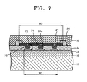
- FIG. 7 is a cross-sectional view of a cladding unit 26 on the driving power bus line 21 according to another embodiment.
- the cladding unit 26 can prevent an aluminum layer of the driving power bus line 21 from being corroded.
- the metal layers 70 according to embodiments depicted in FIGS. 6 and 7 may be formed of the same materials as the gate electrode and may be formed in a single layer, but other configurations may also be used.
- the gate electrode and the source and drain electrodes are formed in a structure of more than three layers, and the metal layer 70 can also have a structure of more than three layers. In this case, an additional cladding unit may be included.
- FIG. 8 is a plan view of an organic light emitting display device according to another embodiment.
- the metal layer 70 can be formed to have a length substantially corresponding to the panel mark 71.
- an additional layout for locating a panel identification mark is unnecessary, thereby reducing the unused area.
- the mark may be associated with electrically operative lines other than power lines, such as signal lines, control lines, and shielding lines.
- the drive voltage drop can also be reduced since the panel identification mark is electrically connected to a driving power bus line.
- a cladding unit covering the side surfaces of a terminal of a pad unit can prevent a conductor from being corroded or etched by an etching solution during a subsequent processing.
Landscapes
- Engineering & Computer Science (AREA)
- Microelectronics & Electronic Packaging (AREA)
- Manufacturing & Machinery (AREA)
- Electroluminescent Light Sources (AREA)
- Devices For Indicating Variable Information By Combining Individual Elements (AREA)
Abstract
Description
- The present invention relates to a flat panel display device, and more particularly, to an organic light emitting display device with reduced unused image area because of a panel identification mark, and with low resistance power bus lines.
- A panel identification mark is included in a flat panel display device such as a liquid crystal display device, an organic light emitting display device, or an inorganic light emitting display device, to allow convenient identification, tracking of the panel, and evaluation of the display cells.
- The panel identification mark is located on a separate area outside the display region where images are displayed. Therefore, the space occupied by the panel identification mark is unused space, where images are not displayed, and the unused space increases in area as the size of the panel identification mark increases.
- Accordingly, in the conventional art, the panel identification mark is usually located in existing unused space, for instance under a driving chip, where it does not affect other signals and does not need additional area.
- However, when the panel identification mark is formed under the driving chip, it is difficult to identify the panel identification mark after the driving chip is mounted. Also, the liquid crystal display device in the conventional art does not supply additional power to each of the pixels. However, in the case of an active matrix (AM) organic light emitting display device, a power supply line for supplying power to each pixel must be extended. Accordingly, the unused area in the panel is further increased. Therefore, it is difficult to lay out the panel identification mark without increasing the unused area of the panel.
- An organic light emitting display device that reduces unused area and reduces a drive voltage drop is disclosed.
- The above and other features and advantages will become more apparent with disclosure of embodiments discussed with reference to the attached drawings in which:
- FIG. 1 is a plan view of an organic light emitting display device according to an embodiment;
- FIG. 2 is a schematic diagram of a unit pixel of an organic light emitting display device including a pixel circuit according to an embodiment;
- FIG. 3 is a detailed schematic diagram of the unit pixel of FIG. 2;
- FIG. 4 is cross-sectional view of the circuit of FIG. 3;
- FIG. 5 is a partial enlarged plan view of a panel mark of FIG. 1;
- FIG. 6 is a cross-sectional view taken along line VI-VI of FIG. 1;
- FIG. 7 is a modified version of the cross-section of FIG. 6; and
- FIG. 8 is a plan view of an organic light emitting display device according to another embodiment.
- Certain embodiments will now be described more fully with reference to the accompanying drawings.
- FIG. 1 is a plan view of an active matrix (AM) organic light emitting display device according to an embodiment.
- Referring to FIG. 1, a
display region 2 where images are displayed is formed on asubstrate 31. Thedisplay region 2 is sealed by an additional sealing member (not shown) to protect thedisplay region 2 from impact, moisture, and air. The sealing member may be, for example, an insulating substrate or a metal cap. - A
terminal region 1 comprising terminals is located on an end portion of thesubstrate 31 where thedisplay region 2 is formed. Theterminal region 1 is exposed outside the sealing member. - Around the
display region 2, there are arranged a drivingpower bus line 21 for supplying driving power to aVdd line 20, an electrodepower bus line 22 connected to a facingelectrode 53 to supply facing electrode power, andvarious circuits display region 2. - Areas where the
terminal region 1, the drivingpower bus line 21, the electrodepower bus line 22, and thecircuits - The driving
power bus line 21 is formed to surround theentire display region 2 from an end of a drivingpower terminal unit 11 to the other end of the drivingpower terminal unit 11, and also, is disposed in a lower side of thedisplay region 2 by being connected through drivingpower lines Vdd 20 that cross thedisplay region 2. - The electrode
power bus line 22, which is electrically connected to an electrode of the organic light emitting display device in thedisplay region 2 and will be described in detail later, is formed on a side of thedisplay region 2. The electrode connected to the electrodepower bus line 22 can be extended to cover the electrodepower bus line 22. An insulating film is interposed between the electrode connected to the electrodepower bus line 22 and the electrodepower bus line 22, and the electrode and the electrodepower bus line 22 are connected through a plurality ofcontact holes 25. - The
vertical circuit unit 23 and thehorizontal circuit unit 24 are mounted between the drivingpower bus line 21 and thedisplay region 2. Thevertical circuit unit 23 can be a scan driving circuit unit that applies scan signals to gate lines of thedisplay region 2, and is electrically connected to ascan terminal unit 13 in theterminal region 1. Thehorizontal circuit unit 24 can be a data driving circuit unit that applies data signals to data lines of thedisplay region 2, and is electrically connected to adata terminal unit 14 in theterminal region 1. Thevertical circuit unit 23 and thehorizontal circuit unit 24 can be formed on thesubstrate 31 using a patterning method, or can include an external IC or COG. - The
display region 2 includes a plurality of pixels, each of which can have a pixel circuit as depicted in FIG. 2. - Referring to FIG. 2, each pixel includes a data line Data, a scan line Scan, and a power supply line Vdd that supplies driving power to an organic light emitting diode (OLED). The supply line Vdd corresponds to a driving
power line Vdd 20 of FIG. 1. - The pixel circuit PC of each pixel is electrically connected to the data line, the scan line Scan, and the supply line Vdd, and controls the light emission of the OLED. FIG. 3 is a detailed schematic diagram of the unit pixel of FIG. 2. The pixel circuit PC of each pixel includes two thin film transistors M1 and M2 and one capacitor unit Cst.
- Referring to FIG. 3, each pixel of the organic light emitting display device according to an embodiment, includes at least two thin film transistors (TFTs), i.e. a switching TFT M2 and a driving TFT M1, a capacitor unit Cst, and an OLED.
- The switching TFT M2 is turned on or off by a scan signal applied to a scan line Scan to transmit a data signal applied to the data line Data to the storage capacitor unit Cst and the driving TFT M1. According to embodiments of the present invention, the switching device is not limited to the switching TFT M2 depicted in FIG. 4, and can be a switching circuit having a plurality of TFTs and capacitors, or can further include a circuit that compensates for a threshold voltage Vth value of the driving TFT M1 or a circuit that compensates for a voltage drop of the Vdd power line Vdd.
- The driving TFT M1 determines the current input to the OLED according to a data signal transmitted through the switching TFT M2.
- The capacitor unit Cst stores the data signal transmitted from the switching TFT M2 for one frame period.
- In the circuit diagram of FIG. 3, the driving TFT M1 and the switching TFT M2 are depicted as PMOS TFTs, but other transistors may also be used. One or both of the driving TFT M1 and the switching TFT M2 can be an NMOS TFT. Also, the number of TFTs and capacitors is not limited to that shown in FIG. 3, and can be increased as necessary.
- In one embodiment, the pixel circuit PC has a cross-sectional structure as depicted in FIG. 4. FIG. 4 is a cross-sectional view of a portion of the pixel of FIG. 3. Referring to FIG. 4, a TFT 40 and an OLED are included on a
substrate 31. - The
substrate 31 can be formed of acryl, polyimide, polycarbonate, polyester, mylar, or a plastic material, but embodiments are not limited to these materials, and thesubstrate 31 can be formed of a metal foil such as SUS, tungsten, etc., glass or another material or combination of materials. - Although not depicted, a barrier layer and/or a buffer layer can be formed on the upper surface of the
substrate 31 to prevent the diffusion of impurity ions, prevent the penetration of moisture or external air, and/or planarize the surface. - An
active layer 41 of the TFT 40 is formed on theinsulating layer 32 using a semiconductor material, and agate insulating film 33 is formed to cover theactive layer 41. Theactive layer 41 can be formed of an inorganic semiconductor material such as amorphous silicon, polysilicon, or an organic semiconductor material. Theactive layer 41 includes achannel region 411 between asource region 412 and adrain region 413. - A
gate electrode 42 is formed on thegate insulating film 33, and aninterlayer insulating film 34 covering thegate electrode 42 is formed. Asource electrode 43 and adrain electrode 44 are formed on theinterlayer insulating film 34. Apassivation film 35 and apixel defining film 37 are sequentially formed to cover thesource electrode 43 and thedrain electrode 44. - The
gate insulating film 33, theinterlayer insulating film 34, thepassivation film 35, and thepixel defining film 37 can each have a single layer structure or a multi-layer structure, and can be formed of an organic material, an inorganic material, or a composite of organic and inorganic materials. - The stacking structure of a TFT according to these embodiments is not limited to that of the
TFT 40, and various TFT structures can be used. - A
pixel electrode 51, which is an electrode of the OLED, is formed on thepassivation film 35, and apixel defining film 37 is formed on thepixel electrode 51. After exposing thepixel electrode 51 through apredetermined opening 38 in thepixel defining film 37, an organiclight emitting film 52 of the OLED is formed. - The OLED emits red, green, or blue light according to the current supplied to form a predetermined image, and comprises the
pixel electrode 51 that contacts thedrain electrode 44 of theTFT 40 through acontact hole 36, a facingelectrode 53 covering all of the pixels, and the organiclight emitting film 52, which is located between thepixel electrode 51 and the facingelectrode 53 and emits light. - The
pixel electrode 51 and the facingelectrode 53 are insulated from each other by the organiclight emitting film 52, and apply voltages of opposite polarity to the organiclight emitting film 52 so that the organiclight emitting film 52 emits light. - The organic
light emitting film 52 can be, for example, a small molecular weight organic film or a polymer organic film. If the organiclight emitting film 52 is a small molecular weight organic film, the organiclight emitting film 52 can include a hole injection Layer (HIL), a hole transport layer (HTL), an emission layer (EML), an electron transport layer (ETL), or an electron injection layer (EIL), can be stacked in a single structure or a composite structure, and can be composed of copper phthalocyanine (CuPc), N,N'-di(naphthalene-1-yl)-N,N'-diphenyl-benzidine (NPB), or tris-8-hydroxyquinoline aluminum (Alq3). The small molecular weight organic film can be formed using a vacuum evaporation method. The HIL, the HTL, the ETL, and the EIL are common electrodes, and can be commonly formed in red, green, and blue pixels. Accordingly, the common electrodes can cover the pixels like the facingelectrode 53. - If the organic
light emitting film 52 is formed of a polymer organic film, the organiclight emitting film 52 can include a HTL and an EML. The HTL can be formed of PEDOT, and the EML can be formed of poly-phenylenevinylene (PPV) and polyfluorene. The polymer organic film can be formed by screen printing, ink jet printing, etc. - The organic
light emitting film 52 is not limited to the configuration described above, and can take various forms. - The
pixel electrode 51 functions as an anode electrode, and the facingelectrode 52 functions as a cathode electrode. In some embodiments, the polarity of thepixel electrode 51 and the facingelectrode 53 may be reversed. - In the case of a bottom emission type display device, the
pixel electrode 51 can be a transparent electrode, and the facingelectrode 53 can be a reflective electrode. Thepixel electrode 51 can comprise a transparent material having a high work function, such as, but not limited to ITO, IZO, In2O3, or ZnO, and the facingelectrode 53 can comprise a reflective metal having a low work function, such as, but not limited to Ag, Mg, Al, Pt, Pd, Au, Ni, Nd, Ir, Cr, Li, Ca, or a compound of these metals. - In the case of a top emission type display device, the
pixel electrode 51 can be a reflective electrode, and the facingelectrode 53 can be a transparent electrode. Thepixel electrode 51 can be formed of a material having a high work function such as, but not limited to, ITO, IZO, In2O3, or ZnO after forming a reflective film using Ag, Mg, Al, Pt, Pd, Au, Ni, Nd, Ir, Cr, Li, Ca, or a compound of these metals. The facingelectrode 53 can include a material layer comprising a metal having a low work function, such as, but not limited to, Li, Ca, LiF/Ca, LiF/Al, Al, Ag, Mg, or a compound of these metals, and an auxiliary electrode layer or a bus electrode line comprising a transparent conductive material, such as, but not limited to, ITO, IZO, ZnO or In2O3, formed on the material layer. - In the case of a double sided emission type display device, both the
pixel electrode 51 and the facingelectrode 53 can be transparent electrodes. - The materials for forming the
pixel electrode 51 and the facingelectrode 53 are not limited to the materials described above. For example, thepixel electrode 51 and the facingelectrode 53 can be formed of a conductive paste containing a conductive organic material or conductive particles of Ag, Mg, Cu, etc. When the conductive paste is used, the paste can be printed by inkjet printing and annealed to form an electrode. - After the OLED is formed, the upper part of the OLED is sealed to substantially prevent exposure to the atmosphere.
- In some embodiments, the
gate electrode 42, thesource electrode 43, and thedrain electrode 44 can comprise a metal such as Ag, Mg, Al, Pt, Pd, Au, Ni, Nd, Ir, Cr, Li, Ca, a compound of these metals, or a transparent conductive material, such as ITO, IZO, ZnO or In2O3 as the conductor described above. Also, thegate electrode 42, thesource electrode 43, and thedrain electrode 44 can comprise a conductive paste containing a conductive organic material or conductive particles of Ag, Mg, Cu, etc. In the OLED according to the embodiment illustrated in FIG. 4, thegate electrode 42 has a single layer structure, thesource electrode 43 and thedrain electrode 44 have a three-layer structure, but embodiments are not limited to these structures. Thegate electrode 42 can also have a three-layer structure. Hereinafter, the description will focus mainly on embodiments in which thegate electrode 42 has a single layer structure and thesource electrode 43 and thedrain electrode 44 have a three-layer structure as depicted in FIG. 5. - The source electrode 43 can have a stacked structure including first, second and third
conductive layers drain electrode 44 can have a stacked structure including first, second, and thirdconductive layers conductive layers - When the second
conductive layers conductive layers conductive layers - In one embodiment, the first
conductive layers conductive layers conductive layers - When the second
conductive layers conductive layers conductive layers - In one embodiment, the first
conductive layers conductive layers conductive layers - However, the conductive layers are not limited thereto, and a layer structure can further be included in addition to the three layer structure.
- As shown in FIG. 4, when the
source electrode 43 and thedrain electrode 44 are formed in a multi-layer structure, acladding unit 45 can be formed of an insulating material to cap the side of thesource electrode 43 and thedrain electrode 44. When thecladding unit 45 is formed of an organic material, the organic material can comprise a polymer derivative having a phenol group, an acryl group polymer, an imide group polymer, an arylether group polymer, an amide group polymer, a fluorine group polymer, a p-xylyrene group polymer, a vinyl alcohol group polymer, and a composition of more than one of these materials. In some embodiments, thepassivation film 35 can be formed of an acryl material, for example, a photosensitive acryl material that can be easily patterned. When thecladding unit 45 is formed of an inorganic material, the inorganic material can comprise at least one of SiO2, SiNx, SiON, Al2O3, TiO2, Ta2O5, HfO2, ZrO2, Barium Strontium Titanate (BST), and PZT. - As described above, since the
source electrode 43 and thedrain electrode 44 have a multilayer structure, the overall conductivity of thesource electrode 43 and thedrain electrode 44 can be improved. This occurs because the secondconductive layers conductive layers conductive layers conductive layers cladding unit 45 can prevent the secondconductive layers source electrode 43 and thedrain electrode 44. Thecladding unit 45 is particularly useful for protecting thesource electrode 43 and thedrain electrode 44 from the penetration of an etchant when thepixel electrode 51 is patterned. The cladding may also be used for electrically operative lines other than power lines, such as signal lines, control lines, and shielding lines. AVdd line 20 can also be formed when thesource electrode 43 and thedrain electrode 44 are formed. The Vdd line formed at the same time as thesource electrode 43 and thedrain electrode 44 also has a firstconductive layer 201, a secondconductive layer 202, and a thirdconductive layer 203. The firstconductive layer 201, the secondconductive layer 202, and the thirdconductive layer 203 can be formed of the same materials described above. - A
cladding unit 25 can also be formed in theVdd line 20 as described above. The function of thecladding unit 25 is the same as that of thecladding unit 45, thus a detailed description thereof will be omitted. - When the
source electrode 43 and thedrain electrode 44 are formed, a plurality of conductors can be formed in addition to theVdd line 20 in the pixel. For example, the drivingpower bus line 21 and the electrodepower bus line 22 shown in FIG. 1 can be formed at the same time. - In some embodiments, a
metal layer 70 overlaps the drivingpower bus line 21 and connects electrically to the drivingpower bus line 21. Themetal layer 70 can be formed, for example, adjacent to the drivingpower bus line 21 and have a length substantially corresponding to the drivingpower bus line 21. Themetal layer 70 may be long enough to reduce the voltage drop of the drivingpower bus line 21, which will be described later. - The
metal layer 70 can be formed at the same time as thegate electrode 42 of theTFT 40 shown in FIG. 4, and accordingly, can be formed of the same materials as thegate electrode 42. - The
metal layer 70 may have a width W1 smaller than the width W2 of the drivingpower bus line 21. Accordingly, as shown in FIG. 1, themetal layer 70 can be completely covered by the drivingpower bus line 21. Accordingly, unused area is not increased by themetal layer 70. - The
metal layer 70 may be used to form apanel mark 71 which is an identification mark for identifying the panel. As shown in FIG. 5, thepanel mark 71 can be formed withopenings 72 by engraving themetal layer 70, but other techniques may also be used. For example, a mark can be engraved on themetal layer 70 using a laser etc. - Referring to FIG. 6, the
metal layer 70 is separated from the drivingpower bus line 21 by aninterlayer insulating film 34 interposed therebetween. However,contact holes 34a are formed in theinterlayer insulating film 34 so that the drivingpower bus line 21 can contact themetal layer 70. Accordingly, themetal layer 70 and the drivingpower bus line 21 are electrically connected, thereby reducing sheet resistance. Accordingly, the IR drop, i.e. voltage drop of the drivingpower bus line 21 can be reduced. - FIG. 7 is a cross-sectional view of a
cladding unit 26 on the drivingpower bus line 21 according to another embodiment. As described above, thecladding unit 26 can prevent an aluminum layer of the drivingpower bus line 21 from being corroded. The metal layers 70 according to embodiments depicted in FIGS. 6 and 7 may be formed of the same materials as the gate electrode and may be formed in a single layer, but other configurations may also be used. In some embodiments, the gate electrode and the source and drain electrodes are formed in a structure of more than three layers, and themetal layer 70 can also have a structure of more than three layers. In this case, an additional cladding unit may be included. - FIG. 8 is a plan view of an organic light emitting display device according to another embodiment. Referring to FIG. 8, the
metal layer 70 can be formed to have a length substantially corresponding to thepanel mark 71. - The above embodiments are described with respect to an organic light emitting display device, but the inventive aspects can be applied to various flat panel display devices such as a liquid crystal display.
- According to described embodiments, an additional layout for locating a panel identification mark is unnecessary, thereby reducing the unused area. Various modifications can be made. For example, the mark may be associated with electrically operative lines other than power lines, such as signal lines, control lines, and shielding lines.
- The drive voltage drop can also be reduced since the panel identification mark is electrically connected to a driving power bus line.
- A cladding unit covering the side surfaces of a terminal of a pad unit can prevent a conductor from being corroded or etched by an etching solution during a subsequent processing.
- While the embodiments described herein have been particularly shown and described with reference to several examples, it will be understood by those of ordinary skill in the art that various changes in form and detail may be made therein without departing from the scope of the invention as defined by the claims.
Claims (18)
- A flat panel display device comprising:a pixel region;an electrically operative line located outside of the pixel region, the electrically operative line comprising a panel identification mark.
- A device according to claim 1, further comprising a metal layer electrically connected to the electrically operative line, the metal layer comprising the panel identification mark.
- A device according to claim 1 or 2, wherein the electrically operative line comprises a power bus line, a signal line, a control line and/or a shielding line.
- A device according to claim 2, wherein the display device comprises an organic light emitting display device, wherein the pixel region comprises a plurality of organic light emitting diodes and the electrically operative line comprises a power bus line configured to supply power to each of the organic light emitting diodes.
- A device according to claim 4, wherein an insulating layer is positioned between the metal layer and the power bus line, and the metal layer and the power bus line contact each other through contact holes formed in the insulating layer.
- A device according to claim 4 or 5, wherein the pixel region comprises a plurality of thin film transistors respectively electrically connected to the organic light emitting diodes, the thin film transistors each comprising a source electrode, a drain electrode, and a gate electrode, wherein the power bus line is formed of the same material as the source and drain electrodes of the thin film transistors, and the metal layer is formed of the same material as the gate electrodes of the thin film transistors.
- A device according to claim 4, 5 or 6, wherein at least one of the power bus line and the metal layer comprises, sequentially stacked, a first conductive layer, a second conductive layer, and a third conductive layer, wherein the second conductive layer comprises at least one of aluminium and aluminium alloy.
- A device according to claim 7, wherein at least one of the first conductive layer and the third conductive layer comprises at least one of Cr, Cr alloy, Mo, Mo alloy, W, and W alloy.
- A device according to claim 7, wherein at least one of the first conductive layer and the third conductive layer comprises at least one of Ti, Ti alloy, Ta, and Ta alloy.
- A device according to any one of claims 4 to 9, further comprising a cladding unit configured to cover at least a side of the power bus line.
- A device according to claim 10, wherein the cladding unit comprises at least one of a polymer derivative comprising a phenol group, an acryl group polymer, an imide group polymer, an arylether group polymer, an amide group polymer, a fluorine group polymer, a p-xylyrene group polymer, a vinyl alcohol group polymer, and a combination of these materials.
- A device according to claim 10, wherein the cladding unit comprises an inorganic material.
- A device according to claim 12, wherein the cladding unit is formed of at least one material selected from the group consisting of SiO2, SiNx, SiON, Al2O3, TiO2, Ta2O5, HfO2, ZrO2, Barium Strontium Titanate (BST), and PZT.
- A device according to any one of claims 4 to 13, wherein the metal layer is formed within the width of the power bus line.
- A device according to any one of claims 4 to 13, wherein the metal layer is located adjacent to the driving power bus line.
- A device according to any one of claims 4 to 15, wherein the metal layer has a length substantially corresponding to the length of the power bus line.
- A device according to any one of claims 2 to 16, wherein the panel identification mark is formed by removing portions of the metal layer.
- A device according to any one of claims 2 to 16, wherein the panel identification mark is formed by the metal layer.
Applications Claiming Priority (1)
| Application Number | Priority Date | Filing Date | Title |
|---|---|---|---|
| KR1020050107028A KR100647712B1 (en) | 2005-11-09 | 2005-11-09 | Organic light emitting display |
Publications (3)
| Publication Number | Publication Date |
|---|---|
| EP1786039A2 true EP1786039A2 (en) | 2007-05-16 |
| EP1786039A3 EP1786039A3 (en) | 2012-11-28 |
| EP1786039B1 EP1786039B1 (en) | 2018-02-21 |
Family
ID=37712923
Family Applications (1)
| Application Number | Title | Priority Date | Filing Date |
|---|---|---|---|
| EP06123684.0A Active EP1786039B1 (en) | 2005-11-09 | 2006-11-08 | Flat Panel Display Device |
Country Status (4)
| Country | Link |
|---|---|
| US (1) | US7919918B2 (en) |
| EP (1) | EP1786039B1 (en) |
| KR (1) | KR100647712B1 (en) |
| CN (1) | CN1964062B (en) |
Families Citing this family (33)
| Publication number | Priority date | Publication date | Assignee | Title |
|---|---|---|---|---|
| US7839079B2 (en) * | 2007-02-20 | 2010-11-23 | Lg Display Co., Ltd. | Organic light emitting display preventing voltage or current dropdown in power conductive lines |
| JP5007170B2 (en) * | 2007-07-20 | 2012-08-22 | 株式会社ジャパンディスプレイイースト | Organic EL display device |
| WO2010047217A1 (en) * | 2008-10-24 | 2010-04-29 | Semiconductor Energy Laboratory Co., Ltd. | Semiconductor device and method for manufacturing the same |
| KR101333783B1 (en) | 2009-11-10 | 2013-11-29 | 삼성디스플레이 주식회사 | Organic light emitting diode display and method for manufacturing the same |
| KR101135540B1 (en) * | 2009-11-30 | 2012-04-13 | 삼성모바일디스플레이주식회사 | Organic Light Emitting Display Device |
| CN102097452B (en) * | 2010-11-09 | 2012-07-25 | 友达光电股份有限公司 | Light source device |
| US9060397B2 (en) * | 2011-07-15 | 2015-06-16 | General Electric Company | High voltage LED and driver |
| US8704232B2 (en) | 2012-06-12 | 2014-04-22 | Apple Inc. | Thin film transistor with increased doping regions |
| US9065077B2 (en) | 2012-06-15 | 2015-06-23 | Apple, Inc. | Back channel etch metal-oxide thin film transistor and process |
| US9685557B2 (en) | 2012-08-31 | 2017-06-20 | Apple Inc. | Different lightly doped drain length control for self-align light drain doping process |
| US8987027B2 (en) | 2012-08-31 | 2015-03-24 | Apple Inc. | Two doping regions in lightly doped drain for thin film transistors and associated doping processes |
| US8748320B2 (en) | 2012-09-27 | 2014-06-10 | Apple Inc. | Connection to first metal layer in thin film transistor process |
| US8999771B2 (en) | 2012-09-28 | 2015-04-07 | Apple Inc. | Protection layer for halftone process of third metal |
| US9201276B2 (en) | 2012-10-17 | 2015-12-01 | Apple Inc. | Process architecture for color filter array in active matrix liquid crystal display |
| US9001297B2 (en) | 2013-01-29 | 2015-04-07 | Apple Inc. | Third metal layer for thin film transistor with reduced defects in liquid crystal display |
| US9088003B2 (en) | 2013-03-06 | 2015-07-21 | Apple Inc. | Reducing sheet resistance for common electrode in top emission organic light emitting diode display |
| TWI523217B (en) * | 2013-09-12 | 2016-02-21 | 友達光電股份有限公司 | Pixel structure |
| CN103715231B (en) | 2013-12-31 | 2016-11-23 | 京东方科技集团股份有限公司 | Organic electroluminescence display panel, display device |
| JP6302683B2 (en) * | 2014-01-29 | 2018-03-28 | パイオニア株式会社 | Light emitting device |
| KR102242214B1 (en) * | 2014-03-05 | 2021-04-21 | 삼성디스플레이 주식회사 | Display device and method for manufacturing the same |
| KR102204378B1 (en) * | 2014-09-04 | 2021-01-19 | 삼성디스플레이 주식회사 | Display device and driving method of the same |
| KR102490881B1 (en) * | 2014-12-26 | 2023-01-25 | 삼성디스플레이 주식회사 | Organic light emitting display device and manufacturing method of the same |
| CN105679795B (en) * | 2015-12-31 | 2018-11-09 | 上海天马有机发光显示技术有限公司 | Display panel and display device |
| KR102550322B1 (en) * | 2016-03-22 | 2023-07-03 | 삼성디스플레이 주식회사 | Display device and manufacturing method thereof |
| KR102562898B1 (en) * | 2016-03-31 | 2023-08-04 | 삼성디스플레이 주식회사 | Display Device |
| CN109390351B (en) | 2017-08-02 | 2021-01-22 | 京东方科技集团股份有限公司 | Wiring structure and preparation method thereof, OLED array substrate and display device |
| CN111149434B (en) * | 2017-09-28 | 2022-07-05 | 夏普株式会社 | Display device and method for manufacturing the same |
| KR102516058B1 (en) * | 2018-08-17 | 2023-03-31 | 삼성디스플레이 주식회사 | Display panel |
| CN208781850U (en) * | 2018-10-31 | 2019-04-23 | 京东方科技集团股份有限公司 | Display base plate, display panel and display device |
| KR102631169B1 (en) * | 2018-12-31 | 2024-01-29 | 엘지디스플레이 주식회사 | Electroluminance Lighting Device |
| CN114175132B (en) * | 2019-08-09 | 2023-08-15 | 夏普株式会社 | Display device |
| CN113299722B (en) * | 2021-05-31 | 2024-08-16 | 福州京东方显示技术有限公司 | Display panel |
| CN115050315B (en) * | 2022-06-30 | 2025-01-28 | 厦门天马显示科技有限公司 | Display panel and display device |
Citations (2)
| Publication number | Priority date | Publication date | Assignee | Title |
|---|---|---|---|---|
| US20020131004A1 (en) | 2001-03-14 | 2002-09-19 | Makoto Watanabe | Liquid crystal display apparatus with address marks connected to connections |
| US6597427B1 (en) | 1999-07-06 | 2003-07-22 | International Business Machines Corporation | Liquid crystal panel, display device, identification mark detection device, detection display system, TFT array repair device and identification mark detection method |
Family Cites Families (10)
| Publication number | Priority date | Publication date | Assignee | Title |
|---|---|---|---|---|
| US5799080A (en) * | 1995-07-13 | 1998-08-25 | Lsi Logic Corporation | Semiconductor chip having identification/encryption code |
| JPH10209581A (en) | 1997-01-24 | 1998-08-07 | Seiko Epson Corp | Printed wiring board, liquid crystal display device and electronic equipment |
| JP3117010B2 (en) * | 1998-11-05 | 2000-12-11 | 日本電気株式会社 | LCD panel |
| KR100675319B1 (en) * | 2000-12-23 | 2007-01-26 | 엘지.필립스 엘시디 주식회사 | Electro luminescence panel |
| TWI257496B (en) * | 2001-04-20 | 2006-07-01 | Toshiba Corp | Display device and method of manufacturing the same |
| JP2002367523A (en) | 2001-06-12 | 2002-12-20 | Matsushita Electric Ind Co Ltd | Plasma display panel and method of manufacturing plasma display panel |
| KR20040058840A (en) | 2002-12-27 | 2004-07-05 | 엘지.필립스 엘시디 주식회사 | An array substrate for Liquid crystal display and method for fabricating the same |
| KR100544123B1 (en) * | 2003-07-29 | 2006-01-23 | 삼성에스디아이 주식회사 | Flat Panel Display |
| CN100428521C (en) * | 2003-11-17 | 2008-10-22 | 富士施乐株式会社 | Organic Semiconductor Transistor Elements |
| JP2005283830A (en) | 2004-03-29 | 2005-10-13 | Seiko Epson Corp | Mounting structure, electro-optical device, electronic apparatus, mounting structure inspection method, electro-optical device inspection method |
-
2005
- 2005-11-09 KR KR1020050107028A patent/KR100647712B1/en not_active Expired - Lifetime
-
2006
- 2006-10-09 CN CN2006101359125A patent/CN1964062B/en active Active
- 2006-10-31 US US11/590,558 patent/US7919918B2/en active Active
- 2006-11-08 EP EP06123684.0A patent/EP1786039B1/en active Active
Patent Citations (2)
| Publication number | Priority date | Publication date | Assignee | Title |
|---|---|---|---|---|
| US6597427B1 (en) | 1999-07-06 | 2003-07-22 | International Business Machines Corporation | Liquid crystal panel, display device, identification mark detection device, detection display system, TFT array repair device and identification mark detection method |
| US20020131004A1 (en) | 2001-03-14 | 2002-09-19 | Makoto Watanabe | Liquid crystal display apparatus with address marks connected to connections |
Also Published As
| Publication number | Publication date |
|---|---|
| US20070103063A1 (en) | 2007-05-10 |
| CN1964062A (en) | 2007-05-16 |
| CN1964062B (en) | 2010-08-11 |
| EP1786039B1 (en) | 2018-02-21 |
| EP1786039A3 (en) | 2012-11-28 |
| KR100647712B1 (en) | 2006-11-23 |
| US7919918B2 (en) | 2011-04-05 |
Similar Documents
| Publication | Publication Date | Title |
|---|---|---|
| EP1786039B1 (en) | Flat Panel Display Device | |
| US7838880B2 (en) | Flat panel display device | |
| JP4974661B2 (en) | Flat panel display and method of manufacturing flat panel display | |
| US7593086B2 (en) | Flexible flat panel display | |
| US8030838B2 (en) | Organic light emitting display apparatus | |
| US7510891B2 (en) | Organic light emitting display device and method of manufacturing the same | |
| EP1503422B1 (en) | Flat panel display | |
| EP1722268A1 (en) | Flat panel display and method of manufacturing the same | |
| KR100922762B1 (en) | Flat Panel Display and Organic Light Emitting Display | |
| US12082458B2 (en) | Display device having a conductive layer of a same material as the pixel electrode covering one side surface of a power supply line formed under a sealing portion between two substrates | |
| KR100813840B1 (en) | Organic light emitting display | |
| KR100777728B1 (en) | Flat panel display | |
| KR100626087B1 (en) | Organic light emitting display | |
| KR100719556B1 (en) | Flexible printed circuit board and flat panel display device having same | |
| KR100741101B1 (en) | Flat panel display | |
| KR100719568B1 (en) | OLED display and manufacturing method thereof |
Legal Events
| Date | Code | Title | Description |
|---|---|---|---|
| PUAI | Public reference made under article 153(3) epc to a published international application that has entered the european phase |
Free format text: ORIGINAL CODE: 0009012 |
|
| 17P | Request for examination filed |
Effective date: 20061108 |
|
| AK | Designated contracting states |
Kind code of ref document: A2 Designated state(s): AT BE BG CH CY CZ DE DK EE ES FI FR GB GR HU IE IS IT LI LT LU LV MC NL PL PT RO SE SI SK TR |
|
| AX | Request for extension of the european patent |
Extension state: AL BA HR MK YU |
|
| RAP1 | Party data changed (applicant data changed or rights of an application transferred) |
Owner name: SAMSUNG MOBILE DISPLAY CO., LTD. |
|
| RAP1 | Party data changed (applicant data changed or rights of an application transferred) |
Owner name: SAMSUNG MOBILE DISPLAY CO., LTD. |
|
| RAP1 | Party data changed (applicant data changed or rights of an application transferred) |
Owner name: SAMSUNG DISPLAY CO., LTD. |
|
| PUAL | Search report despatched |
Free format text: ORIGINAL CODE: 0009013 |
|
| AK | Designated contracting states |
Kind code of ref document: A3 Designated state(s): AT BE BG CH CY CZ DE DK EE ES FI FR GB GR HU IE IS IT LI LT LU LV MC NL PL PT RO SE SI SK TR |
|
| AX | Request for extension of the european patent |
Extension state: AL BA HR MK RS |
|
| RIC1 | Information provided on ipc code assigned before grant |
Ipc: H01L 27/32 20060101AFI20121024BHEP |
|
| AKX | Designation fees paid |
Designated state(s): DE FR GB |
|
| RAP1 | Party data changed (applicant data changed or rights of an application transferred) |
Owner name: SAMSUNG DISPLAY CO., LTD. |
|
| STAA | Information on the status of an ep patent application or granted ep patent |
Free format text: STATUS: EXAMINATION IS IN PROGRESS |
|
| 17Q | First examination report despatched |
Effective date: 20170113 |
|
| GRAP | Despatch of communication of intention to grant a patent |
Free format text: ORIGINAL CODE: EPIDOSNIGR1 |
|
| STAA | Information on the status of an ep patent application or granted ep patent |
Free format text: STATUS: GRANT OF PATENT IS INTENDED |
|
| INTG | Intention to grant announced |
Effective date: 20170830 |
|
| GRAS | Grant fee paid |
Free format text: ORIGINAL CODE: EPIDOSNIGR3 |
|
| GRAA | (expected) grant |
Free format text: ORIGINAL CODE: 0009210 |
|
| STAA | Information on the status of an ep patent application or granted ep patent |
Free format text: STATUS: THE PATENT HAS BEEN GRANTED |
|
| AK | Designated contracting states |
Kind code of ref document: B1 Designated state(s): DE FR GB |
|
| REG | Reference to a national code |
Ref country code: GB Ref legal event code: FG4D |
|
| REG | Reference to a national code |
Ref country code: DE Ref legal event code: R096 Ref document number: 602006054732 Country of ref document: DE |
|
| REG | Reference to a national code |
Ref country code: FR Ref legal event code: PLFP Year of fee payment: 13 |
|
| REG | Reference to a national code |
Ref country code: DE Ref legal event code: R097 Ref document number: 602006054732 Country of ref document: DE |
|
| PLBE | No opposition filed within time limit |
Free format text: ORIGINAL CODE: 0009261 |
|
| STAA | Information on the status of an ep patent application or granted ep patent |
Free format text: STATUS: NO OPPOSITION FILED WITHIN TIME LIMIT |
|
| 26N | No opposition filed |
Effective date: 20181122 |
|
| REG | Reference to a national code |
Ref country code: DE Ref legal event code: R079 Ref document number: 602006054732 Country of ref document: DE Free format text: PREVIOUS MAIN CLASS: H01L0027320000 Ipc: H10K0059000000 |
|
| P01 | Opt-out of the competence of the unified patent court (upc) registered |
Effective date: 20230515 |
|
| PGFP | Annual fee paid to national office [announced via postgrant information from national office to epo] |
Ref country code: DE Payment date: 20241021 Year of fee payment: 19 |
|
| PGFP | Annual fee paid to national office [announced via postgrant information from national office to epo] |
Ref country code: GB Payment date: 20241021 Year of fee payment: 19 |
|
| PGFP | Annual fee paid to national office [announced via postgrant information from national office to epo] |
Ref country code: FR Payment date: 20241022 Year of fee payment: 19 |