EP1785766B1 - A light-emitting device comprising porous alumina, and corresponding method of fabrication - Google Patents
A light-emitting device comprising porous alumina, and corresponding method of fabrication Download PDFInfo
- Publication number
- EP1785766B1 EP1785766B1 EP07102992A EP07102992A EP1785766B1 EP 1785766 B1 EP1785766 B1 EP 1785766B1 EP 07102992 A EP07102992 A EP 07102992A EP 07102992 A EP07102992 A EP 07102992A EP 1785766 B1 EP1785766 B1 EP 1785766B1
- Authority
- EP
- European Patent Office
- Prior art keywords
- layer
- alumina
- electroluminescent material
- pores
- electrode
- Prior art date
- Legal status (The legal status is an assumption and is not a legal conclusion. Google has not performed a legal analysis and makes no representation as to the accuracy of the status listed.)
- Expired - Lifetime
Links
- PNEYBMLMFCGWSK-UHFFFAOYSA-N aluminium oxide Inorganic materials [O-2].[O-2].[O-2].[Al+3].[Al+3] PNEYBMLMFCGWSK-UHFFFAOYSA-N 0.000 title claims abstract description 62
- 238000004519 manufacturing process Methods 0.000 title claims description 4
- 239000000758 substrate Substances 0.000 claims abstract description 33
- 230000005670 electromagnetic radiation Effects 0.000 claims abstract description 15
- 239000000463 material Substances 0.000 claims description 40
- 239000011148 porous material Substances 0.000 claims description 19
- 239000004411 aluminium Substances 0.000 claims description 9
- 229910052782 aluminium Inorganic materials 0.000 claims description 9
- XAGFODPZIPBFFR-UHFFFAOYSA-N aluminium Chemical compound [Al] XAGFODPZIPBFFR-UHFFFAOYSA-N 0.000 claims description 9
- 238000000034 method Methods 0.000 claims description 7
- 239000004065 semiconductor Substances 0.000 claims description 5
- 230000008021 deposition Effects 0.000 claims description 3
- 239000002159 nanocrystal Substances 0.000 claims description 2
- 239000004020 conductor Substances 0.000 claims 4
- 238000007743 anodising Methods 0.000 claims 1
- 239000013335 mesoporous material Substances 0.000 claims 1
- 238000000605 extraction Methods 0.000 abstract 1
- 239000004038 photonic crystal Substances 0.000 description 16
- 230000005855 radiation Effects 0.000 description 16
- 230000000694 effects Effects 0.000 description 5
- 238000005424 photoluminescence Methods 0.000 description 4
- MUBZPKHOEPUJKR-UHFFFAOYSA-N Oxalic acid Chemical compound OC(=O)C(O)=O MUBZPKHOEPUJKR-UHFFFAOYSA-N 0.000 description 3
- 230000015572 biosynthetic process Effects 0.000 description 3
- 239000013078 crystal Substances 0.000 description 3
- 238000000151 deposition Methods 0.000 description 3
- 230000005764 inhibitory process Effects 0.000 description 3
- 239000011159 matrix material Substances 0.000 description 3
- 230000000737 periodic effect Effects 0.000 description 3
- 230000002269 spontaneous effect Effects 0.000 description 3
- NBIIXXVUZAFLBC-UHFFFAOYSA-N Phosphoric acid Chemical compound OP(O)(O)=O NBIIXXVUZAFLBC-UHFFFAOYSA-N 0.000 description 2
- GWEVSGVZZGPLCZ-UHFFFAOYSA-N Titan oxide Chemical compound O=[Ti]=O GWEVSGVZZGPLCZ-UHFFFAOYSA-N 0.000 description 2
- 238000002048 anodisation reaction Methods 0.000 description 2
- 230000003247 decreasing effect Effects 0.000 description 2
- 239000003792 electrolyte Substances 0.000 description 2
- 239000011521 glass Substances 0.000 description 2
- 238000005286 illumination Methods 0.000 description 2
- 230000003993 interaction Effects 0.000 description 2
- 238000004544 sputter deposition Methods 0.000 description 2
- 239000000126 substance Substances 0.000 description 2
- CIWBSHSKHKDKBQ-JLAZNSOCSA-N Ascorbic acid Chemical compound OC[C@H](O)[C@H]1OC(=O)C(O)=C1O CIWBSHSKHKDKBQ-JLAZNSOCSA-N 0.000 description 1
- QAOWNCQODCNURD-UHFFFAOYSA-N Sulfuric acid Chemical compound OS(O)(=O)=O QAOWNCQODCNURD-UHFFFAOYSA-N 0.000 description 1
- 230000002378 acidificating effect Effects 0.000 description 1
- 229910000147 aluminium phosphate Inorganic materials 0.000 description 1
- 230000004888 barrier function Effects 0.000 description 1
- 239000003990 capacitor Substances 0.000 description 1
- 238000000576 coating method Methods 0.000 description 1
- 238000010276 construction Methods 0.000 description 1
- 239000003989 dielectric material Substances 0.000 description 1
- 239000002019 doping agent Substances 0.000 description 1
- 238000005530 etching Methods 0.000 description 1
- 239000012535 impurity Substances 0.000 description 1
- AMGQUBHHOARCQH-UHFFFAOYSA-N indium;oxotin Chemical compound [In].[Sn]=O AMGQUBHHOARCQH-UHFFFAOYSA-N 0.000 description 1
- 238000011835 investigation Methods 0.000 description 1
- 230000014759 maintenance of location Effects 0.000 description 1
- 229910052751 metal Inorganic materials 0.000 description 1
- 239000002184 metal Substances 0.000 description 1
- 239000007769 metal material Substances 0.000 description 1
- 229910044991 metal oxide Inorganic materials 0.000 description 1
- 150000004706 metal oxides Chemical class 0.000 description 1
- 230000003287 optical effect Effects 0.000 description 1
- 235000006408 oxalic acid Nutrition 0.000 description 1
- 230000003647 oxidation Effects 0.000 description 1
- 238000007254 oxidation reaction Methods 0.000 description 1
- 235000011007 phosphoric acid Nutrition 0.000 description 1
- 239000010453 quartz Substances 0.000 description 1
- 229910052710 silicon Inorganic materials 0.000 description 1
- 239000010703 silicon Substances 0.000 description 1
- VYPSYNLAJGMNEJ-UHFFFAOYSA-N silicon dioxide Inorganic materials O=[Si]=O VYPSYNLAJGMNEJ-UHFFFAOYSA-N 0.000 description 1
- 239000007787 solid Substances 0.000 description 1
- 238000003756 stirring Methods 0.000 description 1
- 239000001117 sulphuric acid Substances 0.000 description 1
- 235000011149 sulphuric acid Nutrition 0.000 description 1
- 238000003786 synthesis reaction Methods 0.000 description 1
- 238000011282 treatment Methods 0.000 description 1
- 238000001429 visible spectrum Methods 0.000 description 1
Images

Classifications
-
- G—PHYSICS
- G02—OPTICS
- G02F—OPTICAL DEVICES OR ARRANGEMENTS FOR THE CONTROL OF LIGHT BY MODIFICATION OF THE OPTICAL PROPERTIES OF THE MEDIA OF THE ELEMENTS INVOLVED THEREIN; NON-LINEAR OPTICS; FREQUENCY-CHANGING OF LIGHT; OPTICAL LOGIC ELEMENTS; OPTICAL ANALOGUE/DIGITAL CONVERTERS
- G02F1/00—Devices or arrangements for the control of the intensity, colour, phase, polarisation or direction of light arriving from an independent light source, e.g. switching, gating or modulating; Non-linear optics
- G02F1/01—Devices or arrangements for the control of the intensity, colour, phase, polarisation or direction of light arriving from an independent light source, e.g. switching, gating or modulating; Non-linear optics for the control of the intensity, phase, polarisation or colour
- G02F1/13—Devices or arrangements for the control of the intensity, colour, phase, polarisation or direction of light arriving from an independent light source, e.g. switching, gating or modulating; Non-linear optics for the control of the intensity, phase, polarisation or colour based on liquid crystals, e.g. single liquid crystal display cells
- G02F1/133—Constructional arrangements; Operation of liquid crystal cells; Circuit arrangements
- G02F1/1333—Constructional arrangements; Manufacturing methods
- G02F1/1335—Structural association of cells with optical devices, e.g. polarisers or reflectors
- G02F1/1336—Illuminating devices
- G02F1/133602—Direct backlight
-
- B—PERFORMING OPERATIONS; TRANSPORTING
- B82—NANOTECHNOLOGY
- B82Y—SPECIFIC USES OR APPLICATIONS OF NANOSTRUCTURES; MEASUREMENT OR ANALYSIS OF NANOSTRUCTURES; MANUFACTURE OR TREATMENT OF NANOSTRUCTURES
- B82Y20/00—Nanooptics, e.g. quantum optics or photonic crystals
-
- G—PHYSICS
- G02—OPTICS
- G02B—OPTICAL ELEMENTS, SYSTEMS OR APPARATUS
- G02B5/00—Optical elements other than lenses
-
- G—PHYSICS
- G02—OPTICS
- G02B—OPTICAL ELEMENTS, SYSTEMS OR APPARATUS
- G02B6/00—Light guides; Structural details of arrangements comprising light guides and other optical elements, e.g. couplings
- G02B6/10—Light guides; Structural details of arrangements comprising light guides and other optical elements, e.g. couplings of the optical waveguide type
- G02B6/12—Light guides; Structural details of arrangements comprising light guides and other optical elements, e.g. couplings of the optical waveguide type of the integrated circuit kind
- G02B6/122—Basic optical elements, e.g. light-guiding paths
- G02B6/1225—Basic optical elements, e.g. light-guiding paths comprising photonic band-gap structures or photonic lattices
-
- H—ELECTRICITY
- H01—ELECTRIC ELEMENTS
- H01J—ELECTRIC DISCHARGE TUBES OR DISCHARGE LAMPS
- H01J61/00—Gas-discharge or vapour-discharge lamps
- H01J61/02—Details
- H01J61/025—Associated optical elements
-
- H—ELECTRICITY
- H10—SEMICONDUCTOR DEVICES; ELECTRIC SOLID-STATE DEVICES NOT OTHERWISE PROVIDED FOR
- H10K—ORGANIC ELECTRIC SOLID-STATE DEVICES
- H10K50/00—Organic light-emitting devices
- H10K50/80—Constructional details
- H10K50/85—Arrangements for extracting light from the devices
-
- H—ELECTRICITY
- H10—SEMICONDUCTOR DEVICES; ELECTRIC SOLID-STATE DEVICES NOT OTHERWISE PROVIDED FOR
- H10K—ORGANIC ELECTRIC SOLID-STATE DEVICES
- H10K59/00—Integrated devices, or assemblies of multiple devices, comprising at least one organic light-emitting element covered by group H10K50/00
- H10K59/80—Constructional details
- H10K59/875—Arrangements for extracting light from the devices
-
- G—PHYSICS
- G02—OPTICS
- G02B—OPTICAL ELEMENTS, SYSTEMS OR APPARATUS
- G02B2207/00—Coding scheme for general features or characteristics of optical elements and systems of subclass G02B, but not including elements and systems which would be classified in G02B6/00 and subgroups
- G02B2207/107—Porous materials, e.g. for reducing the refractive index
-
- G—PHYSICS
- G02—OPTICS
- G02F—OPTICAL DEVICES OR ARRANGEMENTS FOR THE CONTROL OF LIGHT BY MODIFICATION OF THE OPTICAL PROPERTIES OF THE MEDIA OF THE ELEMENTS INVOLVED THEREIN; NON-LINEAR OPTICS; FREQUENCY-CHANGING OF LIGHT; OPTICAL LOGIC ELEMENTS; OPTICAL ANALOGUE/DIGITAL CONVERTERS
- G02F1/00—Devices or arrangements for the control of the intensity, colour, phase, polarisation or direction of light arriving from an independent light source, e.g. switching, gating or modulating; Non-linear optics
- G02F1/01—Devices or arrangements for the control of the intensity, colour, phase, polarisation or direction of light arriving from an independent light source, e.g. switching, gating or modulating; Non-linear optics for the control of the intensity, phase, polarisation or colour
- G02F1/13—Devices or arrangements for the control of the intensity, colour, phase, polarisation or direction of light arriving from an independent light source, e.g. switching, gating or modulating; Non-linear optics for the control of the intensity, phase, polarisation or colour based on liquid crystals, e.g. single liquid crystal display cells
- G02F1/133—Constructional arrangements; Operation of liquid crystal cells; Circuit arrangements
- G02F1/1333—Constructional arrangements; Manufacturing methods
- G02F1/1335—Structural association of cells with optical devices, e.g. polarisers or reflectors
- G02F1/1336—Illuminating devices
- G02F1/133602—Direct backlight
- G02F1/133606—Direct backlight including a specially adapted diffusing, scattering or light controlling members
- G02F1/133607—Direct backlight including a specially adapted diffusing, scattering or light controlling members the light controlling member including light directing or refracting elements, e.g. prisms or lenses
-
- G—PHYSICS
- G02—OPTICS
- G02F—OPTICAL DEVICES OR ARRANGEMENTS FOR THE CONTROL OF LIGHT BY MODIFICATION OF THE OPTICAL PROPERTIES OF THE MEDIA OF THE ELEMENTS INVOLVED THEREIN; NON-LINEAR OPTICS; FREQUENCY-CHANGING OF LIGHT; OPTICAL LOGIC ELEMENTS; OPTICAL ANALOGUE/DIGITAL CONVERTERS
- G02F1/00—Devices or arrangements for the control of the intensity, colour, phase, polarisation or direction of light arriving from an independent light source, e.g. switching, gating or modulating; Non-linear optics
- G02F1/01—Devices or arrangements for the control of the intensity, colour, phase, polarisation or direction of light arriving from an independent light source, e.g. switching, gating or modulating; Non-linear optics for the control of the intensity, phase, polarisation or colour
- G02F1/13—Devices or arrangements for the control of the intensity, colour, phase, polarisation or direction of light arriving from an independent light source, e.g. switching, gating or modulating; Non-linear optics for the control of the intensity, phase, polarisation or colour based on liquid crystals, e.g. single liquid crystal display cells
- G02F1/133—Constructional arrangements; Operation of liquid crystal cells; Circuit arrangements
- G02F1/1333—Constructional arrangements; Manufacturing methods
- G02F1/1335—Structural association of cells with optical devices, e.g. polarisers or reflectors
- G02F1/1336—Illuminating devices
- G02F1/133625—Electron stream lamps
-
- G—PHYSICS
- G02—OPTICS
- G02F—OPTICAL DEVICES OR ARRANGEMENTS FOR THE CONTROL OF LIGHT BY MODIFICATION OF THE OPTICAL PROPERTIES OF THE MEDIA OF THE ELEMENTS INVOLVED THEREIN; NON-LINEAR OPTICS; FREQUENCY-CHANGING OF LIGHT; OPTICAL LOGIC ELEMENTS; OPTICAL ANALOGUE/DIGITAL CONVERTERS
- G02F2202/00—Materials and properties
- G02F2202/32—Photonic crystals
-
- H—ELECTRICITY
- H10—SEMICONDUCTOR DEVICES; ELECTRIC SOLID-STATE DEVICES NOT OTHERWISE PROVIDED FOR
- H10H—INORGANIC LIGHT-EMITTING SEMICONDUCTOR DEVICES HAVING POTENTIAL BARRIERS
- H10H20/00—Individual inorganic light-emitting semiconductor devices having potential barriers, e.g. light-emitting diodes [LED]
- H10H20/80—Constructional details
- H10H20/872—Periodic patterns for optical field-shaping, e.g. photonic bandgap structures
Definitions
- the present invention relates to light-emitting devices in particular of the backlight type which comprise a transparent substrate having a front surface and a rear surface, there being associated to the rear surface means for generating a visible light radiation which is able to pass through the substrate and come out of the front surface.
- a film of porous alumina is formed on a layer of aluminium and an electroluminescent material is embedded in the pores of alumina, which are then sealed by an ITO film operating as anode.
- the layer of aluminium is used as a cathode for operating the device by field emission effect, according to the Fowler-Nordheim formula.
- a similar light emitting device is disclosed in US 2002/053871 A1 , wherein an organic electroluminescent material is hosted in a metal oxide porous body differing from alumina.
- Gaponenko NV et al "High-effciency luminescent sources fabricated in mesoporous anodic alumina by sol-gel synthesis", Journal of the Society for Information Display, Vol 11, No. 1, 2003, pages 27-32 , reports investigation of photoluminescence from lathanide-doped microporous xerogel solids confined in porous anodic alumina.
- a light emitting device is disclosed, having a substrate on the front surface of which the alumina layer is arranged, hosting the xerogels. This device is excited frontally through UV radiation, to induce photoluminescence in th exerogels.
- the article shows how, with the proposed structure, xerogel photoluminescence is enhanced and increases with the thickness of the porous anodic alumina.
- xerogel photoluminescence is enhanced and increases with the thickness of the porous anodic alumina.
- the authors assume that a photonic band gap effect could be obtained by the structure, with possible enhancement of emission at certain directions and its inhibition at other direction.
- the Latter was also reported in Gaponenko NV et al: "Photoluminescence of Eu-doped titania Xerogel spin-on deposited on porous anodic alumina", Sensors and Actuators A99 (2002), pages 71-73.
- the purpose of the present invention is to provide backlight devices and systems in which the visible electromagnetic radiation produced by a light source can be directed in an optimal way.
- the device comprises
- the present invention is based upon recognition of the fact that particular photonic-crystal structures can be combined with light sources used as backlight in applications in the field of displays and systems for illumination in order to direct light radiation in an optimal way.
- photonic crystals originates from the works of Yablonovitch and results in the possibility of obtaining materials with characteristics such as to influence the properties of photons, as likewise semiconductor crystals influence the properties of electrons.
- the electrons that move in a semiconductor crystal are affected by a periodic potential generated by the interaction with the nuclei of the atoms that constitute the crystal itself. This interaction results in the formation of a series of allowed energy bands, separated by forbidden energy bands.
- photonic crystals which are generally made up of blocks of transparent dielectric material containing an orderly series of microcavities in which there is trapped air or another means having a refractive index very different from the one of the host matrix.
- the difference between the refractive indices causes confinement of photons with given wavelengths within the cavities of the photonic crystal.
- PBGs photonic band gaps
- the properties of a photonic crystal are defined by the periodicity of the materials with different dielectric constants along one or more axes.
- porous alumina is particularly attractive as a PBG material for use in backlight applications.
- films of porous alumina have attracted attention for applications such as dielectric films in aluminium capacitors, and films for retention of organic coatings and for protection of aluminium substrates.
- porous alumina provides an excellent two-dimensional photonic crystal, which is periodic along two of its axes and homogeneous along the third, is exploited.
- the structure of such a photonic crystal can be idealized as a lattice of hollow columns formed by air and embedded in an alumina matrix.
- Porous alumina can be obtained by means of anodization of sheets of high-purity aluminium or of aluminium films on substrates such as glass, quartz, silicon, etc.
- Figure 1 illustrates, purely by way of example, a portion ot a film of porous alumina 1, obtained by means of anodic oxidation of a film of aluminium on a suitable substrate, designated by S.
- the layer of alumina 1 is formed by a series of hexagonal cells C directly adjacent to one another, each having a straight central hole which constitutes a pore P, substantially perpendicular to the surface of the substrate S.
- each cell C that is in a position corresponding to the substrate S has a closing portion having a substantially hemispherical shape, the set of closing portions forming, as a whole, a non-porous part T of the film 1.
- the film of porous alumina 1 can be obtained with a controlled morphology by appropriately choosing the electrolyte and the physical, chemical and electrochemical parameters of the process: in acidic electrolytes (such as phosphoric acid, oxalic acid and sulphuric acid) and in adequate process conditions (voltage, current, stirring, and temperature), it is possible to obtain porous films having a high regularity.
- acidic electrolytes such as phosphoric acid, oxalic acid and sulphuric acid
- adequate process conditions voltage, current, stirring, and temperature
- the dimensions and density of the cells C, the diameter of the pores P and the height of the film of porous alumina 1 can be varied; for example, the typical diameter of the pores P, which is 50 - 400 nm, can be increased or decreased by means of chemical treatments.
- the periodicity of the photonic crystal, and hence the alternation of media with different dielectric constants produces a photonic band gap and, consequently, does not enable propagation of radiation within a specific waveband and in certain directions.
- the size of and the spacing between the pores P S of the photonic crystal constituted by the film of alumina 1 there can be obtained a band gap in a waveband belonging to the visible spectrum for all the directions of propagation lying in the plane of the substrate.
- Figure 2 is a schematic illustration of the effect of directing visible light radiation that can be obtained by applying a film made of porous alumina 1 of a thickness that can range between a few tens of nanometres and a few microns on a portion of the front surface of a transparent substrate or support 2, made, for instance, of glass, which forms part of a backlight device.
- the rear surface of the support 2 emits visible radiation with a substantially lambertian emission lobe (for example, on account of organic or inorganic electroluminescent or photoluminescent materials deposited on said surface).
- a substantially lambertian emission lobe for example, on account of organic or inorganic electroluminescent or photoluminescent materials deposited on said surface.
- the emission lobe LL of the light emitted from the front surface of the support 2 is still substantially lambertian; however, a considerable fraction of the radiation emitted from the rear surface of the support is unable to come out of the front surface in so far as the angle formed between the direction of propagation and the normal to said surface is greater than the angle of total internal reflection (TIR). Said fraction remains trapped within the plate and propagates by total internal reflection until it reaches the perimeter of the plate itself.
- TIR total internal reflection
- FIG. 2 shows, instead, how a film of porous alumina 1 inhibits propagation of light in the directions that form with the normal to the surfaces of the support 2 angles greater than the TIR angle, i.e., directions at which total internal reflection would occur.
- the fraction of radiation corresponding to said directions of propagation is hence converted into radiation, which propagates with angles, with respect to the normal, that are smaller than the TIR angle and substantially manages to come out of the front surface of the plate.
- the net effect is more light extracted from the backlight device and, at the same time, a narrowing of the emission lobe LR of the light coming out of the front surface of the support.
- Inhibition of propagation in directions with an angle greater than the TIR angle is linked to the photonic band gap of porous alumina in the plane of the substrate. Inhibition is complete only for directions of propagation lying in the plane of the substrate (i.e., for an angle of 90° with respect to the normal), but the effect extends in a gradually decreasing way also to smaller angles.
- Figure 3 illustrates by way of example a first embodiment of a light-emitting device comprising a film of alumina according to the present invention.
- a transparent resistive layer having the function of anode such as a film of indium tin oxide (ITO) of nanometric thickness, designated by 3.
- ITO indium tin oxide
- a film of transparent porous alumina 1 is subsequently obtained, by means of anodization of a layer of aluminium, deposited, for example, by vapour deposition or sputtering.
- the structure of the latter is opened at the base, eliminating the non-porous barrier T illustrated in Figure 1 ; this may, for example, be obtained by means of a known etching process.
- the alumina film 1 is subsequently embedded in a layer 4 of a suitable organic or inorganic electroluminescent material, selected, for example, in the group comprising organic phosphors, inorganic and organic semiconductors, metallic nanocrystals, and luminescent rare earths.
- pores of the alumina film 1, which are in the form of through cavities, are hence filled with electroluminescent material 4.
- the device is then completed by depositing a layer 5 of metallic material, having the function of cathode.
- the photonic-crystal structure made with the alumina film 1 directs, according to what has been explained previously, through the support 2 the light radiation generated by the material 4, in such a way that this will come out of the front surface of the support itself in a substantially predetermined direction.
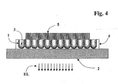
- Figure 4 illustrates a second example of light-emitting device comprising a film of porous alumina according to the present invention.
- the film of transparent alumina 1 is directly obtained on the rear surface of the transparent substrate or support 2, i.e., the surface opposite to the one designed to emit the light.
- the film 1 there is deposited, for example by means of vapour deposition, sputtering or sol-gel, the ITO film 3, so as to coat the internal surfaces of the pores of the anodized alumina.
- the structure thus obtained is embedded in a layer of electroluminescent material 4, on which there is then laid the metal layer 4 having the function of cathode.
- the non-porous part T of the film of transparent alumina 1 is not removed, the ITO film 3 and the cathode 5 being directly in contact with the layer 4 of electroluminescent material.
- the photonic-crystal structure obtained with the alumina film 1 inhibits propagation of radiation at angles greater than the TIR angle, thus directing the radiation generated by the material 4 through the support 2, the said radiation then coming out of the front surface of the latter.
- the transparent resistive layer designated above by 3 may be made up of a metallic percolated layer or by a mesoporous oxide, instead of ITO.
- the light-generating means of the device according to the invention may comprise a layer of photoluminescent phosphors capable of converting UV radiation into visible light.
Landscapes
- Physics & Mathematics (AREA)
- Optics & Photonics (AREA)
- General Physics & Mathematics (AREA)
- Chemical & Material Sciences (AREA)
- Engineering & Computer Science (AREA)
- Nanotechnology (AREA)
- Crystallography & Structural Chemistry (AREA)
- Nonlinear Science (AREA)
- Biophysics (AREA)
- Life Sciences & Earth Sciences (AREA)
- Microelectronics & Electronic Packaging (AREA)
- Mathematical Physics (AREA)
- Electroluminescent Light Sources (AREA)
- Luminescent Compositions (AREA)
- Compositions Of Oxide Ceramics (AREA)
- Catalysts (AREA)
- Illuminated Signs And Luminous Advertising (AREA)
- Led Devices (AREA)
- Road Signs Or Road Markings (AREA)
- Led Device Packages (AREA)
- Planar Illumination Modules (AREA)
Applications Claiming Priority (2)
| Application Number | Priority Date | Filing Date | Title |
|---|---|---|---|
| IT2002TO000670A ITTO20020670A1 (it) | 2002-07-26 | 2002-07-26 | Dispositivo emettitore di luce comprendente allumina porosa e relativo procedimento di realizzazione |
| EP03015861A EP1385041B1 (en) | 2002-07-26 | 2003-07-11 | A light-emitting device comprising porous alumina, and corresponding method of fabrication |
Related Parent Applications (1)
| Application Number | Title | Priority Date | Filing Date |
|---|---|---|---|
| EP03015861A Division EP1385041B1 (en) | 2002-07-26 | 2003-07-11 | A light-emitting device comprising porous alumina, and corresponding method of fabrication |
Publications (2)
| Publication Number | Publication Date |
|---|---|
| EP1785766A1 EP1785766A1 (en) | 2007-05-16 |
| EP1785766B1 true EP1785766B1 (en) | 2009-01-21 |
Family
ID=11459541
Family Applications (2)
| Application Number | Title | Priority Date | Filing Date |
|---|---|---|---|
| EP07102992A Expired - Lifetime EP1785766B1 (en) | 2002-07-26 | 2003-07-11 | A light-emitting device comprising porous alumina, and corresponding method of fabrication |
| EP03015861A Expired - Lifetime EP1385041B1 (en) | 2002-07-26 | 2003-07-11 | A light-emitting device comprising porous alumina, and corresponding method of fabrication |
Family Applications After (1)
| Application Number | Title | Priority Date | Filing Date |
|---|---|---|---|
| EP03015861A Expired - Lifetime EP1385041B1 (en) | 2002-07-26 | 2003-07-11 | A light-emitting device comprising porous alumina, and corresponding method of fabrication |
Country Status (6)
| Country | Link |
|---|---|
| US (2) | US7075229B2 (https=) |
| EP (2) | EP1785766B1 (https=) |
| JP (1) | JP4504640B2 (https=) |
| AT (1) | ATE360229T1 (https=) |
| DE (2) | DE60326019D1 (https=) |
| IT (1) | ITTO20020670A1 (https=) |
Families Citing this family (34)
| Publication number | Priority date | Publication date | Assignee | Title |
|---|---|---|---|---|
| KR100612076B1 (ko) * | 2003-09-08 | 2006-08-11 | 주식회사 엘지화학 | 나노 크기의 반구형 오목부가 형성된 기판을 이용한고효율 유기 발광 소자 및 이의 제조 방법 |
| JP2005174700A (ja) * | 2003-12-10 | 2005-06-30 | Toyota Industries Corp | 電界発光デバイス |
| EP1578173A1 (en) * | 2004-03-18 | 2005-09-21 | C.R.F. Società Consortile per Azioni | Light emitting device comprising porous alumina and manufacturing process thereof |
| US7394587B2 (en) * | 2005-01-28 | 2008-07-01 | Hewlett-Packard Development Company, L.P. | Apparatus having a photonic crystal |
| JP4595565B2 (ja) * | 2005-01-31 | 2010-12-08 | 株式会社デンソー | 自発光表示装置 |
| CN100428396C (zh) * | 2005-09-16 | 2008-10-22 | 清华大学 | 基于多孔氧化铝结构的薄膜阴极场发射显示器件 |
| US20070241326A1 (en) * | 2006-04-18 | 2007-10-18 | Samsung Electronics Co., Ltd. | Organic light emitting diode display and manufacturing method thereof |
| KR100777744B1 (ko) * | 2006-10-27 | 2007-11-19 | 삼성에스디아이 주식회사 | 평판 디스플레이 장치 |
| TWI334660B (en) * | 2007-03-21 | 2010-12-11 | Lextar Electronics Corp | Surface mount type light emitting diode package device and light emitting element package device |
| JP5352171B2 (ja) * | 2007-10-15 | 2013-11-27 | 富士フイルム株式会社 | 発光素子の製造方法および光学素子の製造方法 |
| US20090160314A1 (en) * | 2007-12-20 | 2009-06-25 | General Electric Company | Emissive structures and systems |
| GB2456298A (en) | 2008-01-07 | 2009-07-15 | Anthony Ian Newman | Electroluminescent materials comprising oxidation resistant fluorenes |
| IL206909A0 (en) | 2008-01-11 | 2010-12-30 | Antaria Ltd | Mesoporous zinc oxide powder and method for production thereof |
| US8138675B2 (en) * | 2009-02-27 | 2012-03-20 | General Electric Company | Stabilized emissive structures and methods of making |
| JP2010238486A (ja) * | 2009-03-31 | 2010-10-21 | Fujifilm Corp | 発光素子 |
| WO2010113593A1 (ja) * | 2009-03-31 | 2010-10-07 | 富士フイルム株式会社 | 発光素子 |
| US7927919B1 (en) * | 2009-12-03 | 2011-04-19 | Powertech Technology Inc. | Semiconductor packaging method to save interposer |
| US9991427B2 (en) * | 2010-03-08 | 2018-06-05 | Cree, Inc. | Photonic crystal phosphor light conversion structures for light emitting devices |
| JP5331051B2 (ja) * | 2010-04-21 | 2013-10-30 | パナソニック株式会社 | 発光素子 |
| JP5323257B2 (ja) * | 2010-04-28 | 2013-10-23 | シャープ株式会社 | バックライトユニットおよび液晶表示装置 |
| EP2602356A1 (en) | 2010-08-06 | 2013-06-12 | Mitsubishi Heavy Industries, Ltd. | Vacuum processing apparatus and plasma processing method |
| GB201015417D0 (en) | 2010-09-15 | 2010-10-27 | Lomox Ltd | Organic light emitting diode devices |
| EP2697840A4 (en) * | 2011-04-12 | 2014-11-05 | Arkema Inc | INTERNAL OPTICAL EXTRACTION LAYER FOR OLED DEVICES |
| CN102779831B (zh) * | 2012-07-10 | 2015-09-02 | 京东方科技集团股份有限公司 | 一种有机显示器件及制作的方法 |
| US9226396B2 (en) * | 2013-03-12 | 2015-12-29 | Invensas Corporation | Porous alumina templates for electronic packages |
| US9076790B1 (en) | 2014-01-09 | 2015-07-07 | Taiwan Semiconductor Manufacturing Co., Ltd. | Air gap forming techniques based on anodic alumina for interconnect structures |
| CN105204104B (zh) | 2015-10-30 | 2018-05-25 | 京东方科技集团股份有限公司 | 滤光片及其制作方法、显示基板及显示装置 |
| CN105609535B (zh) * | 2016-01-15 | 2018-11-13 | 京东方科技集团股份有限公司 | 显示基板、显示装置及其制作方法 |
| US11142684B2 (en) * | 2017-02-13 | 2021-10-12 | Philip Taubman Kalisman | Systems and methods for a hermetically sealed quantum dot light emitting diode |
| CN109143438B (zh) * | 2018-10-29 | 2020-08-11 | 福州大学 | 一种基于微纳米多孔结构的量子点彩色滤光膜 |
| WO2020229013A1 (de) * | 2019-05-13 | 2020-11-19 | Osram Opto Semiconductors Gmbh | Multi-chip trägerstruktur |
| CN111129333B (zh) * | 2019-12-30 | 2022-08-19 | 广东聚华印刷显示技术有限公司 | Qled器件、显示装置及qled器件的制备方法 |
| CN114981715A (zh) | 2020-10-19 | 2022-08-30 | 京东方科技集团股份有限公司 | 对置基板、显示面板和显示设备 |
| WO2023132394A1 (ko) * | 2022-01-10 | 2023-07-13 | 엘지전자 주식회사 | 반도체 발광 소자를 이용한 디스플레이 장치 |
Family Cites Families (3)
| Publication number | Priority date | Publication date | Assignee | Title |
|---|---|---|---|---|
| JPH02305886A (ja) * | 1989-05-19 | 1990-12-19 | Nec Corp | 有機薄膜el素子 |
| TW545079B (en) * | 2000-10-26 | 2003-08-01 | Semiconductor Energy Lab | Light emitting device |
| JP2003045661A (ja) * | 2001-08-02 | 2003-02-14 | Fuji Photo Film Co Ltd | 発光性ナノ構造体およびこれを用いた発光素子 |
-
2002
- 2002-07-26 IT IT2002TO000670A patent/ITTO20020670A1/it unknown
-
2003
- 2003-07-11 DE DE60326019T patent/DE60326019D1/de not_active Expired - Lifetime
- 2003-07-11 EP EP07102992A patent/EP1785766B1/en not_active Expired - Lifetime
- 2003-07-11 AT AT03015861T patent/ATE360229T1/de not_active IP Right Cessation
- 2003-07-11 EP EP03015861A patent/EP1385041B1/en not_active Expired - Lifetime
- 2003-07-11 DE DE60313255T patent/DE60313255T2/de not_active Expired - Lifetime
- 2003-07-25 US US10/626,699 patent/US7075229B2/en not_active Expired - Fee Related
- 2003-07-25 JP JP2003279853A patent/JP4504640B2/ja not_active Expired - Fee Related
-
2006
- 2006-06-19 US US11/455,087 patent/US7267596B2/en not_active Expired - Fee Related
Non-Patent Citations (1)
| Title |
|---|
| GAPONENKO N.V. ET AL: "Photoluminescence of Eu-doped titania xerogel spin-on deposited on porous anodic alumina", SENSORS AND ACTUATORS, vol. A99, no. 1-2, 5 June 2001 (2001-06-05), pages 71 - 73, XP002257065 * |
Also Published As
| Publication number | Publication date |
|---|---|
| DE60313255D1 (de) | 2007-05-31 |
| EP1385041A1 (en) | 2004-01-28 |
| US7267596B2 (en) | 2007-09-11 |
| ITTO20020670A0 (it) | 2002-07-26 |
| DE60326019D1 (de) | 2009-03-12 |
| JP2004063470A (ja) | 2004-02-26 |
| US20060252337A1 (en) | 2006-11-09 |
| EP1785766A1 (en) | 2007-05-16 |
| EP1385041B1 (en) | 2007-04-18 |
| ITTO20020670A1 (it) | 2004-01-26 |
| DE60313255T2 (de) | 2008-06-19 |
| ATE360229T1 (de) | 2007-05-15 |
| US7075229B2 (en) | 2006-07-11 |
| JP4504640B2 (ja) | 2010-07-14 |
| US20040150979A1 (en) | 2004-08-05 |
Similar Documents
| Publication | Publication Date | Title |
|---|---|---|
| EP1785766B1 (en) | A light-emitting device comprising porous alumina, and corresponding method of fabrication | |
| JP7203165B2 (ja) | エンハンスメント層を有するoledデバイス | |
| US7776196B2 (en) | Method for arranging particles and method for manufacturing light-emitting device | |
| US7323815B2 (en) | Light-emitting device comprising porous alumina, and manufacturing process thereof | |
| JP6193914B2 (ja) | 有機発光ダイオードディスプレイ装置のための光抽出フィルム | |
| US8355204B2 (en) | Light-extraction layer of light-emitting device and organic electroluminescence element employing the same | |
| US10211419B2 (en) | Organic light emitting diode structure | |
| KR101751685B1 (ko) | 배리어 기능을 가지는 반도체 광원 및 이의 제조방법 | |
| US20160356456A1 (en) | Light-emitting device containing anisotropic flat colloidal semiconductor nanocrystals and methods of manufacture thereof | |
| CN101176214A (zh) | 电致发光光源 | |
| EP3940445B1 (en) | Film, illumination device, projector color wheel and method of manufacturing a film | |
| KR20190077073A (ko) | 도파관, 도파관으로부터 광을 출력 결합하는 방법, 및 디스플레이 | |
| JP6187915B2 (ja) | 有機発光ダイオード、有機発光ダイオード用基板の製造方法、画像表示装置および照明装置 | |
| KR101268534B1 (ko) | 유기 발광 소자 및 유기 발광 소자 제조 방법 | |
| TWI673898B (zh) | 用於有機發光二極體之光萃取基板、製造其之方法、及包含其之有機發光二極體裝置 | |
| CN1447294A (zh) | 一种产生彩色平面发光量子点图形的方法 |
Legal Events
| Date | Code | Title | Description |
|---|---|---|---|
| PUAI | Public reference made under article 153(3) epc to a published international application that has entered the european phase |
Free format text: ORIGINAL CODE: 0009012 |
|
| AC | Divisional application: reference to earlier application |
Ref document number: 1385041 Country of ref document: EP Kind code of ref document: P |
|
| AK | Designated contracting states |
Kind code of ref document: A1 Designated state(s): AT BE BG CH CY CZ DE DK EE ES FI FR GB GR HU IE IT LI LU MC NL PT RO SE SI SK TR |
|
| 17P | Request for examination filed |
Effective date: 20071015 |
|
| 17Q | First examination report despatched |
Effective date: 20071119 |
|
| AKX | Designation fees paid |
Designated state(s): DE ES FR GB IT SE |
|
| GRAP | Despatch of communication of intention to grant a patent |
Free format text: ORIGINAL CODE: EPIDOSNIGR1 |
|
| GRAS | Grant fee paid |
Free format text: ORIGINAL CODE: EPIDOSNIGR3 |
|
| GRAA | (expected) grant |
Free format text: ORIGINAL CODE: 0009210 |
|
| AC | Divisional application: reference to earlier application |
Ref document number: 1385041 Country of ref document: EP Kind code of ref document: P |
|
| AK | Designated contracting states |
Kind code of ref document: B1 Designated state(s): DE ES FR GB IT SE |
|
| REG | Reference to a national code |
Ref country code: GB Ref legal event code: FG4D |
|
| REF | Corresponds to: |
Ref document number: 60326019 Country of ref document: DE Date of ref document: 20090312 Kind code of ref document: P |
|
| PG25 | Lapsed in a contracting state [announced via postgrant information from national office to epo] |
Ref country code: ES Free format text: LAPSE BECAUSE OF FAILURE TO SUBMIT A TRANSLATION OF THE DESCRIPTION OR TO PAY THE FEE WITHIN THE PRESCRIBED TIME-LIMIT Effective date: 20090502 |
|
| PG25 | Lapsed in a contracting state [announced via postgrant information from national office to epo] |
Ref country code: SE Free format text: LAPSE BECAUSE OF FAILURE TO SUBMIT A TRANSLATION OF THE DESCRIPTION OR TO PAY THE FEE WITHIN THE PRESCRIBED TIME-LIMIT Effective date: 20090421 |
|
| PLBE | No opposition filed within time limit |
Free format text: ORIGINAL CODE: 0009261 |
|
| STAA | Information on the status of an ep patent application or granted ep patent |
Free format text: STATUS: NO OPPOSITION FILED WITHIN TIME LIMIT |
|
| 26N | No opposition filed |
Effective date: 20091022 |
|
| REG | Reference to a national code |
Ref country code: FR Ref legal event code: PLFP Year of fee payment: 13 |
|
| PGFP | Annual fee paid to national office [announced via postgrant information from national office to epo] |
Ref country code: DE Payment date: 20150707 Year of fee payment: 13 Ref country code: GB Payment date: 20150708 Year of fee payment: 13 |
|
| PGFP | Annual fee paid to national office [announced via postgrant information from national office to epo] |
Ref country code: FR Payment date: 20150629 Year of fee payment: 13 |
|
| PGFP | Annual fee paid to national office [announced via postgrant information from national office to epo] |
Ref country code: IT Payment date: 20150710 Year of fee payment: 13 |
|
| REG | Reference to a national code |
Ref country code: DE Ref legal event code: R119 Ref document number: 60326019 Country of ref document: DE |
|
| GBPC | Gb: european patent ceased through non-payment of renewal fee |
Effective date: 20160711 |
|
| PG25 | Lapsed in a contracting state [announced via postgrant information from national office to epo] |
Ref country code: FR Free format text: LAPSE BECAUSE OF NON-PAYMENT OF DUE FEES Effective date: 20160801 Ref country code: DE Free format text: LAPSE BECAUSE OF NON-PAYMENT OF DUE FEES Effective date: 20170201 |
|
| REG | Reference to a national code |
Ref country code: FR Ref legal event code: ST Effective date: 20170331 |
|
| PG25 | Lapsed in a contracting state [announced via postgrant information from national office to epo] |
Ref country code: GB Free format text: LAPSE BECAUSE OF NON-PAYMENT OF DUE FEES Effective date: 20160711 |
|
| PG25 | Lapsed in a contracting state [announced via postgrant information from national office to epo] |
Ref country code: IT Free format text: LAPSE BECAUSE OF NON-PAYMENT OF DUE FEES Effective date: 20160711 |