EP1783516B1 - Mikrowellenausrichtungsvorrichtung - Google Patents
Mikrowellenausrichtungsvorrichtung Download PDFInfo
- Publication number
- EP1783516B1 EP1783516B1 EP05024085A EP05024085A EP1783516B1 EP 1783516 B1 EP1783516 B1 EP 1783516B1 EP 05024085 A EP05024085 A EP 05024085A EP 05024085 A EP05024085 A EP 05024085A EP 1783516 B1 EP1783516 B1 EP 1783516B1
- Authority
- EP
- European Patent Office
- Prior art keywords
- microwave
- alignment apparatus
- spacer device
- operable
- antenna system
- Prior art date
- Legal status (The legal status is an assumption and is not a legal conclusion. Google has not performed a legal analysis and makes no representation as to the accuracy of the status listed.)
- Expired - Fee Related
Links
Images


Classifications
-
- G—PHYSICS
- G01—MEASURING; TESTING
- G01S—RADIO DIRECTION-FINDING; RADIO NAVIGATION; DETERMINING DISTANCE OR VELOCITY BY USE OF RADIO WAVES; LOCATING OR PRESENCE-DETECTING BY USE OF THE REFLECTION OR RERADIATION OF RADIO WAVES; ANALOGOUS ARRANGEMENTS USING OTHER WAVES
- G01S7/00—Details of systems according to groups G01S13/00, G01S15/00, G01S17/00
- G01S7/02—Details of systems according to groups G01S13/00, G01S15/00, G01S17/00 of systems according to group G01S13/00
- G01S7/40—Means for monitoring or calibrating
- G01S7/4004—Means for monitoring or calibrating of parts of a radar system
- G01S7/4026—Antenna boresight
-
- G—PHYSICS
- G01—MEASURING; TESTING
- G01S—RADIO DIRECTION-FINDING; RADIO NAVIGATION; DETERMINING DISTANCE OR VELOCITY BY USE OF RADIO WAVES; LOCATING OR PRESENCE-DETECTING BY USE OF THE REFLECTION OR RERADIATION OF RADIO WAVES; ANALOGOUS ARRANGEMENTS USING OTHER WAVES
- G01S13/00—Systems using the reflection or reradiation of radio waves, e.g. radar systems; Analogous systems using reflection or reradiation of waves whose nature or wavelength is irrelevant or unspecified
- G01S13/88—Radar or analogous systems specially adapted for specific applications
- G01S13/93—Radar or analogous systems specially adapted for specific applications for anti-collision purposes
- G01S13/931—Radar or analogous systems specially adapted for specific applications for anti-collision purposes of land vehicles
-
- H—ELECTRICITY
- H01—ELECTRIC ELEMENTS
- H01Q—ANTENNAS, i.e. RADIO AERIALS
- H01Q15/00—Devices for reflection, refraction, diffraction or polarisation of waves radiated from an antenna, e.g. quasi-optical devices
- H01Q15/02—Refracting or diffracting devices, e.g. lens, prism
- H01Q15/08—Refracting or diffracting devices, e.g. lens, prism formed of solid dielectric material
-
- H—ELECTRICITY
- H01—ELECTRIC ELEMENTS
- H01Q—ANTENNAS, i.e. RADIO AERIALS
- H01Q19/00—Combinations of primary active antenna elements and units with secondary devices, e.g. with quasi-optical devices, for giving the antenna a desired directional characteristic
- H01Q19/06—Combinations of primary active antenna elements and units with secondary devices, e.g. with quasi-optical devices, for giving the antenna a desired directional characteristic using refracting or diffracting devices, e.g. lens
- H01Q19/062—Combinations of primary active antenna elements and units with secondary devices, e.g. with quasi-optical devices, for giving the antenna a desired directional characteristic using refracting or diffracting devices, e.g. lens for focusing
-
- H—ELECTRICITY
- H01—ELECTRIC ELEMENTS
- H01Q—ANTENNAS, i.e. RADIO AERIALS
- H01Q9/00—Electrically-short antennas having dimensions not more than twice the operating wavelength and consisting of conductive active radiating elements
- H01Q9/04—Resonant antennas
- H01Q9/0407—Substantially flat resonant element parallel to ground plane, e.g. patch antenna
- H01Q9/0414—Substantially flat resonant element parallel to ground plane, e.g. patch antenna in a stacked or folded configuration
Definitions
- the present invention relates to the field of microwave antenna and particularly to gain or half-power beam widths improving antenna devices in radio frequency of mm-wave (between 30 GHz and 300 GHz) applications by means of lenses and mountings.
- the method of the state of the art to mount such lenses is to use a mechanical holder which is very bulky and in addition influences the performance of the antenna system due to reflection at the metal surfaces. To avoid this effect the engineers tend to increase the diameter and/or dimensions of the lens and/or the lens holder which yields to larger systems. In addition the mounting consists of several components and working steps which yields to a high priced product. Both disadvantages are not preferable for mobile devices.
- Another method of the state of the art is to use the mechanical horn extension of the antenna to mount the lens.
- This solution again does have the disadvantage that the size of the antenna system itself is defined by the waveguide horn and is too big in most applications.
- the manufacturing of a three-dimensional circular or rectangular waveguide horn is much too expensive and therefore not preferable for mobile devices.
- Another method of the state of the art comprises a planar structure with several micro antenna elements whereby a dome type of system is added to the structure creating a lens effect.
- the dielectric constant of the lens material decreases the distances of the patch elements in a way that the design is no longer possible.
- the "big" dome body adds additional dielectric losses to the antenna system, which reduces efficiency and finally gain of the antenna system.
- Another method to control the focus point is to add an additional dielectric material in between the lens and the planar patch antenna, which does have dielectric constant close to air.
- This mounting procedure does have the disadvantages that due to the foam type of such materials, the focus point distance is very difficult to control.
- the lens must be glued to the foam and the foam must be glued to the patch by using e.g. epoxy.
- the epoxy covers areas of the patch elements themselves and therefore influences the performance of the antenna system due to its electrical properties especially for millimeter waves.
- the mounting is very complex (several steps) and therefore too expensive and not preferable for mobile devices.
- Document DE 199 63 003 Al discloses a radar system for motor vehicles with at least one radiation penetrable compound for focusing the sensor rays, whereby at least one arrangement of electrical conductor lines is placed in the radiation penetrable compound, and said arrangement of electrical conductor lines consists of a ferromagnetic material.
- the present invention has the object to provide a microwave alignment apparatus to improve the gain / half-power beam widths / sidelobe of an microwave antenna for mm-wave applications. It is easier and cheaper to manufacture and is smaller than a comparable microwave alignment apparatus of the state of the art. Thus suitable for mobile devices. Therefore the present invention does not need to increase the size of the antenna and/or the lens for better performance due to influences of the mounting compared to the state of the art. Also the microwave alignment apparatus must have less components and should be created out of a smaller range of materials which do not additionally influence the performance. The control of the focus point is only limited to mechanical manufacturing tolerances due to a simple and less material involving arrangement. Additionally there are only very few dielectric losses to the antenna system of the present invention. The mounting to the antenna is only done in areas where no other electrical parts of the antenna are present and therefore no influences concerning performance (gain, frequency behaviour etc.) are given.
- the present invention relates to a microwave alignment apparatus operable to align an electromagnetic wave in the microwave range, which comprises a focusing device operable to focus the electromagnetic wave, a mounting device operable to mount and/or hold the focusing device, whereby said microwave alignment apparatus is formed as one-piece component made from a single material, the mounting device comprises a transparent spacer device operable to be transparent for a microwave and another spacer device operable to connect the focusing device and the transparent spacer device at a specific distance, whereby said transparent spacer device is formed in such a way that the microwaves are incident perpendicular to the transparent spacer device; said transparent spacer device is hollow; and said transparent spacer device is formed as a concavity around a microwave source.
- the microwave alignment apparatus comprises a symmetric axis.
- the spacer device comprises a tube.
- the tube comprises a circular profile.
- the focusing device comprises a planar area perpendicular to the symmetry axis and limited by the tube.
- the focusing device comprises a hole extending from the tube along the symmetry axis.
- the transparent spacer device comprises a concavity with barrier perpendicular to an emitted microwave.
- the concavity comprises a half-sphere.
- the concavity comprises a hole on top of the concavity aligned with the spacer device.
- the focusing device comprises a lens.
- the lens is rotationally symmetric.
- a microwave antenna system comprises a microwave source and a microwave alignment apparatus.
- the microwave source comprises a main lobe.
- the spacer device comprises a lower edge whereby the lower edge relates preferable to the -3dB power point of the main lobe of the microwave source.
- the microwave source comprises a patch antenna.
- the patch antenna is arranged on a multilayer printed circuit board.
- microwave alignment apparatus is connected to the multilayer printed circuit board by connection means.
- connection means comprises epoxy resin and/or clamps and/or glue.
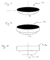
- FIG 1 shows schematical view of an example of a microwave antenna system 7 of the present invention comprising a microwave source 6 and an embodiment of a microwave alignment apparatus 1 of the present invention.
- Figure 8 and Figure 9 show concrete embodiments of the microwave antenna system 7.
- the microwave alignment apparatus 1 comprises a focusing device 3 and a mounting device 2.
- the mounting device 2 comprises a spacer device 5 and a transparent spacer device 4.
- the microwave antenna system 7 is operable to emit and/or receive and amplify the microwaves. It is small enough to be implemented in mobile devices.
- the microwave source 6 is operable to emit and/or receive and emits microwaves, which propagate from one point. It can be implemented as a microwave antenna but can also comprise any other type of microwave source 6 operable to emit and/or receive microwaves e.g. with a frequency between 30 GHz and 300 GHz or any other suitable range. Another possible implementation may comprise microwave sources 6, which emit microwaves from different origins or locations instead from one point.
- the microwave alignment apparatus 1 is operable to align a microwave into a specific direction and to improve gain and half-power beam widths and sidelobe of the microwave source 6 respectively. Hereby, amplification is achieved by focusing the microwave which has a typical frequency between 30 GHz and 300 GHz.
- the microwave alignment apparatus 1 is formed as one-piece component preferably from a single material, which is suitable for the application. Nevertheless it is possible to have different components of the same or different materials of the microwave alignment apparatus 1 which are added together by e.g. glue or plugging the components.
- the microwave alignment apparatus 1 is connected to the microwave source 6 by means which do not (or to a very little extend) deteriorate the performance of the antenna.
- These means may comprise epoxy resin, glue and/or clamping.
- the focusing device 3 is operable to focus a microwave, thus parallelize the from the microwave source 6 emitted microwaves and/or bundle the received microwaves into a focal point which is preferably located at the microwave source 6.
- the focusing device 3 is made of a material preferably for refracting microwaves and formed as an object to provide gain to microwaves.
- the focusing device 3 comprises a lens with a rotationally symmetrical axis operable to focus a microwave point source.
- a lens comprises a straight cylinder cut along its rotational symmetry axis to a half-circular profile which is operable to focus e.g. microwave sources along the symmetry axis of the lens.
- the mounting device 2 is operable to mount and/or hold the focusing device and to arrange the focusing device 3 at a specific distance.
- the mounting device 2 is made of the same material like the focusing device but can be of another material, too.
- the mounting device 2 is hollow to keep the dielectric losses of the microwave as low as possible. At least a part of the mounting device 2 is arranged in such a way that the microwave incident perpendicular to the material; thus no reflection or refraction takes place turning this part quasi invisible and transparent respectively for the microwave.
- the spacer device 5 is operable to arrange the focusing device 3 with the transparent spacer device 4 at a specific distance.
- the spacer device 5 is the upper part of the mounting device 2 and is formed as a tube like a type of cylinder.
- the tube's profile perpendicular to its symmetry axis can be circular or elliptical or any other shape advantageously for the application.
- the diameter of the spacer device 5 is preferable designed in a way that the lower edge is related to the -3dB power point of the farfield pattern of the microwave source 6. For example the edge can touch, cross or keep a specific distance to the -3dB power point depending on the application.
- the spacer device 5 is hollow to keep the dielectric losses of the microwave as low as possible.
- the transparent spacer device 4 is operable to connect to the microwave source 6 without influencing the performance of the microwave antenna system 7.
- the transparent spacer device 4 is the lower part of the mounting device 2 and is formed in such a way that the microwave is incident perpendicular to the transparent spacer device; thus no reflection or refraction takes place turning this device quasi invisible for the microwave.
- the transparent spacer device is hollow to keep the dielectric losses of the microwave as low as possible.
- the transparent spacer device 4 is formed as a concavity around the microwave source 6 like e.g. a patch antenna.
- the concavity can be formed as a half-sphere or any other shape advantageously for the application. But there are other forms of the transparent spacer device 4 possible depending on the radiation pattern of the microwave source 6.
- the focusing device and the mounting device comprise a common symmetry axis.
- FIG 2 shows an example of a spacer device 5a of the present invention.
- the spacer device 5a comprises a hollow cylinder with a circular profile perpendicular to its axis A and has the same functions as the spacer device 5 in Figure 1 .
- FIG 3 shows an example of a focusing device 3a of the present invention.
- the focusing device 3a comprises a planar convex lens with a circular profile perpendicular to its axis B and has the same functions as the focusing device 3 in Figure 1 .
- FIG 4 shows an alternative example of a focusing device 3b of the present invention.
- the focusing device 3b comprises a planar convex lens with a cylindrical attachment and a circular profile perpendicular to its axis C and has the same functions as the focusing device 3 in Figure 1 .
- FIG 5 shows a cross section of an alternative example of a focusing device 3c of the present invention.
- the focusing device 3c comprises a planar convex lens with a cylindrical attachment and a circular profile perpendicular to its axis D and has the same functions as the focusing device 3 in Figure 1 .
- the lens itself comprises a planar area 12 which does not influence the focusing performance fundamentally.
- the planar side is perpendicular to the axis D and is located facing in the other direction than towards the cylindrical attachment.
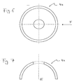
- FIG 6 shows a top view of an example of a transparent spacer device 4a of the present invention.
- the transparent spacer device 4a comprises a half-spherical concavity with a concentric circular hole in the middle of the concavity and has the same functions as the transparent spacer device 4 of Figure 1 .
- FIG 7 shows a cross section of an example of a transparent spacer device 4b of the present invention viewed in direction of arrow F of Figure 6 .
- the transparent spacer device 4b comprises a half-spherical concavity with a around the axis E concentric circular hole on top of the concavity and has the same functions as the transparent spacer device 4 of Figure 1 .
- Figure 8 shows a cross section of an example of a microwave antenna system 7a comprising an embodiment of the microwave alignment apparatus 1a of the present invention and an example of a microwave source 6a.
- the microwave antenna system 7a has the same functions as the microwave antenna system 7 described in Figure 1 .
- the microwave source 6a has the same functions as the microwave source 6 described in Figure 1 .
- the microwave source 6a comprises a patch antenna arranged as four patches on a multilayer board 13 described later in more detail in Figure 10 .
- the multilayer board 13 comprises additionally a microstrip feeding network 16 with feeding elements below the four patches.
- This network 16 is operable to feed electrical energy to the patches via the feeding elements which have the same size as the patches which is described later in more detail in Figure 10 .
- the patch antenna comprises a radiation pattern with a main lobe 14 and two secondary lobes 15 which originate schematically from one point from the middle of the patches.
- the microwave alignment apparatus 1a has the same functions as the microwave alignment apparatus 1 described in Figure 1 .
- the microwave alignment apparatus 1a is manufactured out of one material by e.g. CNC-machining (Computer Numerical Controlled). For further decrease of manufacturing costs, it is possible to created the microwave alignment apparatus out of one component by e.g. plastic injection molding.
- the microwave alignment apparatus is joined to the microwave source 6a, the multilayer board 13 of the patch antenna respectively, by e.g. epoxy resin 8. Other mounting techniques like screwing or clamping are possible, too.
- the mounting of the microwave alignment apparatus 1a of the present invention to the multilayer board 13 can be realised in an area where there is no electrical influence to the patches and so no influence to the electrical performance.
- the transparent spacer device 4c has the same functions as the transparent spacer device 4 described in Figure 1 .
- the transparent spacer device 4c is the lower part of the microwave alignment apparatus 7a and comprises a half sphere. All rays of the patch antenna hit the sphere in the direction of G perpendicular to the surface and therefore no reflection or diffraction of the rays takes place.
- the sphere is hollow to decrease the dielectric losses created by the lens material and to offer an air interface to the patch antenna, so that the patch antenna itself can be checked separately.
- the spacer device 5b is the middle part of the microwave alignment apparatus 7a and comprises a type of cylinder to connect the focusing device 3d to the transparent spacer device 4c.
- the diameter of the tube is preferable designed in a way, so that the lower edge is related to the -3dB power point 9 of the farfield radiation pattern 14 of the patch element itself. It is not mandatory to have this specification for the farfield but can differ from application to application.
- the spacer device 5b is hollow to reduce the dielectric losses within it.
- the focusing device 3d has the same functions as the focusing device 3 described in Figure 1 .
- the shape of the focusing device 3d inside the area of the spacer device 5b is a planar surface 12. Since the microwaves are focus due to the theoretical lens shape 11, the planar surface 12 doesn't remarkable reduces the performance of the focusing device 3d but is easier to manufacture.
- the focusing device and the mounting device comprise a common symmetry axis X and are axial symmetric, but can be also rotational symmetric.
- Figure 9 shows a cross section of an alternative example of a microwave antenna system 7b comprising an alternative embodiment of the microwave alignment apparatus 1b of the present invention and an example of a microwave source 6a.
- the microwave antenna system 7b has the same functions as the microwave antenna system 7 described in Figure 1 .
- the microwave source 6a has the same functions as the microwave source 6a described in Figure 8 .
- the microwave alignment apparatus 1b is the same as the microwave alignment apparatus 1 described in Figure 1 .
- the microwave alignment apparatus 1b is manufactured out of one material by e.g. CNC-machining (Computer Numerical Controlled). For further decrease of manufacturing costs, it is possible to created the microwave alignment apparatus out of one component by e.g. plastic injection molding.
- the microwave alignment apparatus is joined to the microwave source 6a, the multilayer board 13 of the patch antenna respectively, by epoxy resin 8. Other mounting techniques like screwing or clamping are possible, too.
- the mounting of the microwave alignment apparatus 1b of the present invention to the multilayer board 13 can be realised in an area where there is no electrical influence to the patches and so no influence to the electrical performance.
- the transparent spacer device 4c has the same functions as the transparent spacer device 4 described in Figure 1 .
- the transparent spacer device 4c is the lower part of the microwave alignment apparatus 7a and comprises a half sphere. All rays of the patch antenna hit the sphere in the direction of G perpendicular to the surface and therefore no reflection or diffraction of the rays takes place.
- the sphere is hollow to decrease the dielectric losses created by the lens material and to offer an air interface to the patch antenna, so that the patch antenna itself can be checked separately.
- the spacer device 5b is the middle part of the microwave alignment apparatus 7a and comprises a type of cylinder to connect the focusing device 3d to the transparent spacer device 4c.
- the diameter of the tube is preferable designed in a way, so that the lower edge is related to the -3dB power point 9 of the farfield radiation pattern 14 of the patch element itself. It is not mandatory to have this specification for the farfield but can differ from application to application.
- the spacer device 5b is hollow to reduce the dielectric losses within it.
- the focusing device 3e has the same functions as the focusing device 3 described in Figure 1 .
- the hole in the spacer device 5b can be extended to a through-hole 10 going through the focusing device 3e.
- the microwaves are still focus due to the theoretical lens shape 11 with an acceptable degradation of the antenna performance.
- This alternative embodiment is even easier to manufacture than the one described in Figure 8 .
- the focusing device and the mounting device comprise a common symmetry axis X and are axial symmetric, but can be also rotational symmetric.
- Figure 10 shows an example of a microwave source 6 in a top view and figure 11 shows a cross section of figure 10 with the setup of a patch antenna on a multilayer board 13.
- the multilayer board 13 is a PCB (printed circuit board) and comprises four patches 17a, 17b, 17c, 17d, a microstrip feeding network 16a comprising four feeding elements 20a, 20b, 20c, 20d and a via hole 19.
- the four patches 17a, 17b, 17c, 17d have the same size, comprise four square and even surfaces and are parallely arranged to each other forming four gaps 18a, 18b, 18c, 18d between each other. These gaps 18a, 18b, 18c, 18d are open to two opposite arranged sides and limited by the parallely arranged edges of two patches 17a & 17b, 17b &17d, 17d & 17c, 17c & 17a.
- the patches are situated on the top layer of the multilayer board 13.
- the microstrip feeding network 16a is arranged on the next layer under the patches and is operable to feed the patches 17a, 17b, 17c, 17d with electrical energy.
- the feeding elements 20a, 20b, 20c, 20d which are situated right below the patches have the same size as the patches themselves.
- the microstrip feeding network 16a is the same like the one 16 in Figure 8 and 9 .
- the via hole 19 is connecting the microstrip feeding network 16a with a feeding access 21.
- the feeding access 21 comprises a BNC connector.
- the via hole 19, the microstrip feeding network 16a with its feeding elements 20a, 20b, 20c, 20d, the four patches 17a, 17b, 17c, 17d and the feeding access 21 are axial symmetrically arranged along the axis Y.
- a part of the microstrip feeding network 16a and the feeding elements 20c & 20d or 20a & 20b form a common thicker layer, respectively.
- This patch antenna is only an example for a microwave source to be used with the present invention. It should be noted that other kinds of antennas as well as other kinds of patch antennas can be used with the microwave alignment apparatus of the present invention.
Landscapes
- Engineering & Computer Science (AREA)
- Radar, Positioning & Navigation (AREA)
- Remote Sensing (AREA)
- Physics & Mathematics (AREA)
- Computer Networks & Wireless Communication (AREA)
- General Physics & Mathematics (AREA)
- Electromagnetism (AREA)
- Aerials With Secondary Devices (AREA)
- Waveguide Aerials (AREA)
Claims (17)
- Ein Mikrowellen-Ausrichtungsapparat (1), geeignet eine elektromagnetische Welle im Mikrowellenbereich auszurichten,
umfassendeine Fokussierungsvorrichtung (3) geeignet zum Fokussieren der elektromagnetischen Welle,eine Anbauvorrichtung (2) geeignet zum Anbauen und/oder Halten der Fokussierungsvorrichtung (3),wobei der Mikrowellen-Ausrichtungsapparat aus einer einstückigen Komponente aus einem einzigen Material geformt ist, und
die Anbauvorrichtung (2) umfassteinen durchsichtigen Abstandshalter (4), der durchsichtig für Mikrowellen ist,dadurch gekennzeichnet,
dass die Anbauvorrichtung desweiteren umfassteinen weiteren Abstandshalter (5) geeignet zum Verbinden der Fokussierungsvorrichtung (3) und des durchsichtigen Abstandshalters (4) auf eine bestimmte Distanz,wobei der durchsichtige Abstandshalter (4) derart ausgeformt ist, dass die Mikrowellen senkrecht einfallend zum durchsichtigen Abstandshalter sind;der durchsichtige Abstandshalter hohl ist; undder durchsichtige Abstandshalter als Wölbung um die Mikrowellenquelle (6) geformt ist. - Ein Mikrowellen-Ausrichtungsapparat (1) nach Anspruch 1,
wobei der Mikrowellen-Ausrichtungsapparat (1) eine Symmetrieachse hat. - Ein Mikrowellen-Ausrichtungsapparat (1) nach Anspruch 1 oder 2,
wobei der weitere Abstandshalter (5) ein Rohr umfasst. - Ein Mikrowellen-Ausrichtungsapparat (1) nach Anspruch 3,
wobei das Rohr ein rundes Profil hat. - Ein Mikrowellen-Ausrichtungsapparat (1) nach einem der Ansprüche 3 oder 4,
wobei die Fokussierungsvorrichtung (3) eine ebene Fläche (12) umfasst, die senkrecht zu der Symmetrieachse ist und vom Rohr begrenzt wird. - Ein Mikrowellen-Ausrichtungsapparat (1) nach einem der Ansprüche 3 oder 4,
wobei die Fokussierungsvorrichtung (3) ein Loch (10) umfasst, das sich vom Rohr entlang der Symmetrieachse erstreckt. - Ein Mikrowellen-Ausrichtungsapparat (1) nach einem der Ansprüche 1 bis 6,
wobei der durchsichtige Abstandshalter (4) eine konkave Barriere senkrecht zu der ausgestrahlten Mikrowelle umfasst. - Ein Mikrowellen-Ausrichtungsapparat (1) nach Anspruch 7,
wobei die Konkavität eine Halbkugel umfasst. - Ein Mikrowellen-Ausrichtungsapparat (1) nach einem der Ansprüche 7 oder 8,
wobei die Konkavität ein Loch oben auf der Wölbung, das mit dem weiteren Abstandshalter (5) ausgerichtet ist, umfasst. - Ein Mikrowellen-Ausrichtungsapparat (1) nach einem der obengenannten Ansprüche,
wobei die Fokussierungsvorrichtung (3) eine Linse umfasst. - Ein Mikrowellen-Ausrichtungsapparat (1) nach Anspruch 10,
wobei die Linse rotationssymmetrisch ist. - Ein Mikrowellen-Antennen System (7)
umfassendeine Mikrowellenquelle (6) geeignet zum Emittieren und/oder Empfangen elektromagnetischer Wellen im Mikrowellenbereich und einen Mikrowellen-Ausrichtungsapparat (1) nach einer der obengenannten Ansprüche. - Ein Mikrowellen-Antennen System (7) nach Anspruch 12,
wobei die Mikrowellenquelle (6) eine Hauptstrahlungskeule (14) umfasst. - Ein Mikrowellen-Antennen System (7) nach Anspruch 13,
wobei der weitere Abstandshalter (5) eine untere Kante hat,
wobei die untere Kante dem -3dB Energiepunkt (9) der Hauptstrahlungskeule (14) der Mikrowellenquelle (6) entspricht. - Ein Mikrowellen-Antennen System (7) nach einem der Ansprüche 12 bis 14,
wobei die Mikrowellenquelle (6) eine Patchantenne umfasst. - Ein Mikrowellen-Antennen System (7) nach einem der Ansprüche 12 bis 15,
wobei der Mikrowellen-Ausrichtungsapparat mit Hilfe eines Verbindungsmittels (8) mit einer Leiterplatine verbunden ist. - Ein Mikrowellen-Antennen System (7) nach Anspruch 16,
wobei das Verbindungsmittel (8) Epoxid-Harz und/oder Klammern und/oder Kleber und/oder Schrauben umfasst.
Priority Applications (4)
| Application Number | Priority Date | Filing Date | Title |
|---|---|---|---|
| EP05021742A EP1772748A1 (de) | 2005-10-05 | 2005-10-05 | Mikrowellen Ausrichtungsvorrichtung |
| EP05024085A EP1783516B1 (de) | 2005-10-05 | 2005-11-04 | Mikrowellenausrichtungsvorrichtung |
| PCT/EP2006/009604 WO2007039289A1 (en) | 2005-10-05 | 2006-10-04 | Microwave alignment apparatus |
| US12/088,910 US8294627B2 (en) | 2005-10-05 | 2006-10-04 | Microwave alignment apparatus |
Applications Claiming Priority (2)
| Application Number | Priority Date | Filing Date | Title |
|---|---|---|---|
| EP05021742A EP1772748A1 (de) | 2005-10-05 | 2005-10-05 | Mikrowellen Ausrichtungsvorrichtung |
| EP05024085A EP1783516B1 (de) | 2005-10-05 | 2005-11-04 | Mikrowellenausrichtungsvorrichtung |
Publications (2)
| Publication Number | Publication Date |
|---|---|
| EP1783516A1 EP1783516A1 (de) | 2007-05-09 |
| EP1783516B1 true EP1783516B1 (de) | 2010-02-17 |
Family
ID=37459987
Family Applications (2)
| Application Number | Title | Priority Date | Filing Date |
|---|---|---|---|
| EP05021742A Withdrawn EP1772748A1 (de) | 2005-10-05 | 2005-10-05 | Mikrowellen Ausrichtungsvorrichtung |
| EP05024085A Expired - Fee Related EP1783516B1 (de) | 2005-10-05 | 2005-11-04 | Mikrowellenausrichtungsvorrichtung |
Family Applications Before (1)
| Application Number | Title | Priority Date | Filing Date |
|---|---|---|---|
| EP05021742A Withdrawn EP1772748A1 (de) | 2005-10-05 | 2005-10-05 | Mikrowellen Ausrichtungsvorrichtung |
Country Status (3)
| Country | Link |
|---|---|
| US (1) | US8294627B2 (de) |
| EP (2) | EP1772748A1 (de) |
| WO (1) | WO2007039289A1 (de) |
Cited By (1)
| Publication number | Priority date | Publication date | Assignee | Title |
|---|---|---|---|---|
| CN104218318A (zh) * | 2013-05-29 | 2014-12-17 | 华为技术有限公司 | 天线对准方法及装置 |
Families Citing this family (17)
| Publication number | Priority date | Publication date | Assignee | Title |
|---|---|---|---|---|
| US9716320B2 (en) * | 2014-10-10 | 2017-07-25 | Cambium Networks Limited | Patch antenna-based wideband antenna system |
| US10601137B2 (en) | 2015-10-28 | 2020-03-24 | Rogers Corporation | Broadband multiple layer dielectric resonator antenna and method of making the same |
| US11367959B2 (en) | 2015-10-28 | 2022-06-21 | Rogers Corporation | Broadband multiple layer dielectric resonator antenna and method of making the same |
| US10476164B2 (en) | 2015-10-28 | 2019-11-12 | Rogers Corporation | Broadband multiple layer dielectric resonator antenna and method of making the same |
| US10374315B2 (en) | 2015-10-28 | 2019-08-06 | Rogers Corporation | Broadband multiple layer dielectric resonator antenna and method of making the same |
| JP6683539B2 (ja) * | 2016-05-25 | 2020-04-22 | 日立オートモティブシステムズ株式会社 | アンテナ、センサ及び車載システム |
| US11283189B2 (en) | 2017-05-02 | 2022-03-22 | Rogers Corporation | Connected dielectric resonator antenna array and method of making the same |
| US11876295B2 (en) | 2017-05-02 | 2024-01-16 | Rogers Corporation | Electromagnetic reflector for use in a dielectric resonator antenna system |
| CN110754017B (zh) | 2017-06-07 | 2023-04-04 | 罗杰斯公司 | 介质谐振器天线系统 |
| US10892544B2 (en) * | 2018-01-15 | 2021-01-12 | Rogers Corporation | Dielectric resonator antenna having first and second dielectric portions |
| US10910722B2 (en) | 2018-01-15 | 2021-02-02 | Rogers Corporation | Dielectric resonator antenna having first and second dielectric portions |
| US11616302B2 (en) * | 2018-01-15 | 2023-03-28 | Rogers Corporation | Dielectric resonator antenna having first and second dielectric portions |
| US11552390B2 (en) | 2018-09-11 | 2023-01-10 | Rogers Corporation | Dielectric resonator antenna system |
| US11031697B2 (en) | 2018-11-29 | 2021-06-08 | Rogers Corporation | Electromagnetic device |
| WO2020117489A1 (en) | 2018-12-04 | 2020-06-11 | Rogers Corporation | Dielectric electromagnetic structure and method of making the same |
| CN110829035B (zh) * | 2019-11-19 | 2021-03-16 | 大连海事大学 | 一种宽半功率波束的圆极化贴片天线 |
| US11482790B2 (en) | 2020-04-08 | 2022-10-25 | Rogers Corporation | Dielectric lens and electromagnetic device with same |
Family Cites Families (9)
| Publication number | Priority date | Publication date | Assignee | Title |
|---|---|---|---|---|
| JPH066128A (ja) * | 1992-06-19 | 1994-01-14 | Murata Mfg Co Ltd | 誘電体レンズアンテナおよびその製造方法 |
| US5455589A (en) * | 1994-01-07 | 1995-10-03 | Millitech Corporation | Compact microwave and millimeter wave radar |
| ATE217455T1 (de) * | 1995-07-17 | 2002-05-15 | Dynex Semiconductor Ltd | Antennenanordnungen |
| WO1998035403A1 (de) * | 1997-02-06 | 1998-08-13 | Robert Bosch Gmbh | Mikrowellen-antennenanordnung für ein kraftfahrzeug-radarsystem |
| US6590544B1 (en) * | 1998-09-01 | 2003-07-08 | Qualcomm, Inc. | Dielectric lens assembly for a feed antenna |
| SE514076C2 (sv) * | 1999-04-23 | 2000-12-18 | Ericsson Telefon Ab L M | Förfarande och anordning relaterade till mikrovågslins |
| DE19963003A1 (de) * | 1999-12-24 | 2001-06-28 | Bosch Gmbh Robert | Kraftfahrzeug-Radarsystem |
| JP4523223B2 (ja) * | 2002-04-26 | 2010-08-11 | 株式会社日立製作所 | レーダセンサ |
| KR100485354B1 (ko) * | 2002-11-29 | 2005-04-28 | 한국전자통신연구원 | 유전체 덮개를 이용한 마이크로스트립 패치 안테나 및이를 배열한 배열 안테나 |
-
2005
- 2005-10-05 EP EP05021742A patent/EP1772748A1/de not_active Withdrawn
- 2005-11-04 EP EP05024085A patent/EP1783516B1/de not_active Expired - Fee Related
-
2006
- 2006-10-04 US US12/088,910 patent/US8294627B2/en not_active Expired - Fee Related
- 2006-10-04 WO PCT/EP2006/009604 patent/WO2007039289A1/en active Application Filing
Cited By (3)
| Publication number | Priority date | Publication date | Assignee | Title |
|---|---|---|---|---|
| CN104218318A (zh) * | 2013-05-29 | 2014-12-17 | 华为技术有限公司 | 天线对准方法及装置 |
| CN104218318B (zh) * | 2013-05-29 | 2017-08-04 | 华为技术有限公司 | 天线对准方法及装置 |
| US10096886B2 (en) | 2013-05-29 | 2018-10-09 | Huawei Technologies Co., Ltd. | Antenna alignment method and device |
Also Published As
| Publication number | Publication date |
|---|---|
| US8294627B2 (en) | 2012-10-23 |
| EP1783516A1 (de) | 2007-05-09 |
| WO2007039289A1 (en) | 2007-04-12 |
| EP1772748A1 (de) | 2007-04-11 |
| US20090051613A1 (en) | 2009-02-26 |
Similar Documents
| Publication | Publication Date | Title |
|---|---|---|
| EP1783516B1 (de) | Mikrowellenausrichtungsvorrichtung | |
| US9112270B2 (en) | Planar array feed for satellite communications | |
| US9112262B2 (en) | Planar array feed for satellite communications | |
| CN109792109B (zh) | 天线元件 | |
| US7042420B2 (en) | Multi-beam antenna | |
| US8743004B2 (en) | Integrated waveguide cavity antenna and reflector dish | |
| US7518566B2 (en) | Waveguide structure for creating a phase gradient between input signals of a system of antenna elements | |
| US9397407B2 (en) | Antenna system | |
| CN107548527B (zh) | 具有电子电路的反射器和具有反射器的天线装置 | |
| KR20070077464A (ko) | 원형 도파관 안테나 및 원형 도파관 어레이 안테나 | |
| US10651551B2 (en) | Antenna radome-enclosures and related antenna structures | |
| CN110890629B (zh) | 一种低剖面宽角扫描的全金属多波束透镜天线 | |
| US7839349B1 (en) | Tunable substrate phase scanned reflector antenna | |
| KR20020093048A (ko) | 빔 스캐닝용 평면 안테나 | |
| EP2020699A1 (de) | Leckwellenantenne mit sich zwischen parallelen Oberflächen ausbreitenden Wellen | |
| JP3364829B2 (ja) | アンテナ装置 | |
| JP2000341026A (ja) | アンテナ基板及びそれを用いた無線通信機 | |
| JP4027775B2 (ja) | スロットアレーアンテナ | |
| GB2518883A (en) | Antenna system | |
| CN110620288A (zh) | 天线装置及无线装置 | |
| Orakwue et al. | Two dimensional switched beam antenna based on cascaded butler matrix beamforming network | |
| GB2509112A (en) | Antenna system electromagnetic lens arrangement | |
| US20230395998A1 (en) | A dual-polarized radiator arrangement for a mobile communication antenna and a mobile communication antenna comprising at least one dual-polarized radiator arrangement | |
| CN112771726A (zh) | 天线装置 | |
| KR200360060Y1 (ko) | 수지급전 분배 판넬을 사용한 안테나 장치 |
Legal Events
| Date | Code | Title | Description |
|---|---|---|---|
| PUAI | Public reference made under article 153(3) epc to a published international application that has entered the european phase |
Free format text: ORIGINAL CODE: 0009012 |
|
| AK | Designated contracting states |
Kind code of ref document: A1 Designated state(s): AT BE BG CH CY CZ DE DK EE ES FI FR GB GR HU IE IS IT LI LT LU LV MC NL PL PT RO SE SI SK TR |
|
| AX | Request for extension of the european patent |
Extension state: AL BA HR MK YU |
|
| 17P | Request for examination filed |
Effective date: 20071009 |
|
| 17Q | First examination report despatched |
Effective date: 20071107 |
|
| AKX | Designation fees paid |
Designated state(s): DE FR GB |
|
| GRAP | Despatch of communication of intention to grant a patent |
Free format text: ORIGINAL CODE: EPIDOSNIGR1 |
|
| GRAS | Grant fee paid |
Free format text: ORIGINAL CODE: EPIDOSNIGR3 |
|
| GRAA | (expected) grant |
Free format text: ORIGINAL CODE: 0009210 |
|
| AK | Designated contracting states |
Kind code of ref document: B1 Designated state(s): DE FR GB |
|
| REG | Reference to a national code |
Ref country code: GB Ref legal event code: FG4D |
|
| REF | Corresponds to: |
Ref document number: 602005019418 Country of ref document: DE Date of ref document: 20100401 Kind code of ref document: P |
|
| PLBE | No opposition filed within time limit |
Free format text: ORIGINAL CODE: 0009261 |
|
| STAA | Information on the status of an ep patent application or granted ep patent |
Free format text: STATUS: NO OPPOSITION FILED WITHIN TIME LIMIT |
|
| 26N | No opposition filed |
Effective date: 20101118 |
|
| REG | Reference to a national code |
Ref country code: FR Ref legal event code: ST Effective date: 20110801 |
|
| PG25 | Lapsed in a contracting state [announced via postgrant information from national office to epo] |
Ref country code: FR Free format text: LAPSE BECAUSE OF NON-PAYMENT OF DUE FEES Effective date: 20101130 |
|
| PGFP | Annual fee paid to national office [announced via postgrant information from national office to epo] |
Ref country code: DE Payment date: 20121121 Year of fee payment: 8 |
|
| PGFP | Annual fee paid to national office [announced via postgrant information from national office to epo] |
Ref country code: GB Payment date: 20121120 Year of fee payment: 8 |
|
| GBPC | Gb: european patent ceased through non-payment of renewal fee |
Effective date: 20131104 |
|
| PG25 | Lapsed in a contracting state [announced via postgrant information from national office to epo] |
Ref country code: DE Free format text: LAPSE BECAUSE OF NON-PAYMENT OF DUE FEES Effective date: 20140603 |
|
| REG | Reference to a national code |
Ref country code: DE Ref legal event code: R119 Ref document number: 602005019418 Country of ref document: DE Effective date: 20140603 |
|
| PG25 | Lapsed in a contracting state [announced via postgrant information from national office to epo] |
Ref country code: GB Free format text: LAPSE BECAUSE OF NON-PAYMENT OF DUE FEES Effective date: 20131104 |