EP1780660A2 - Semiconductor integrated circuit and contactless electronic device using the same - Google Patents
Semiconductor integrated circuit and contactless electronic device using the same Download PDFInfo
- Publication number
- EP1780660A2 EP1780660A2 EP06022553A EP06022553A EP1780660A2 EP 1780660 A2 EP1780660 A2 EP 1780660A2 EP 06022553 A EP06022553 A EP 06022553A EP 06022553 A EP06022553 A EP 06022553A EP 1780660 A2 EP1780660 A2 EP 1780660A2
- Authority
- EP
- European Patent Office
- Prior art keywords
- voltage
- charge
- charge pump
- pump circuit
- semiconductor integrated
- Prior art date
- Legal status (The legal status is an assumption and is not a legal conclusion. Google has not performed a legal analysis and makes no representation as to the accuracy of the status listed.)
- Granted
Links
Images



Classifications
-
- G—PHYSICS
- G11—INFORMATION STORAGE
- G11C—STATIC STORES
- G11C5/00—Details of stores covered by group G11C11/00
- G11C5/14—Power supply arrangements, e.g. power down, chip selection or deselection, layout of wirings or power grids, or multiple supply levels
-
- G—PHYSICS
- G06—COMPUTING OR CALCULATING; COUNTING
- G06K—GRAPHICAL DATA READING; PRESENTATION OF DATA; RECORD CARRIERS; HANDLING RECORD CARRIERS
- G06K19/00—Record carriers for use with machines and with at least a part designed to carry digital markings
- G06K19/06—Record carriers for use with machines and with at least a part designed to carry digital markings characterised by the kind of the digital marking, e.g. shape, nature, code
- G06K19/067—Record carriers with conductive marks, printed circuits or semiconductor circuit elements, e.g. credit or identity cards also with resonating or responding marks without active components
- G06K19/07—Record carriers with conductive marks, printed circuits or semiconductor circuit elements, e.g. credit or identity cards also with resonating or responding marks without active components with integrated circuit chips
- G06K19/0723—Record carriers with conductive marks, printed circuits or semiconductor circuit elements, e.g. credit or identity cards also with resonating or responding marks without active components with integrated circuit chips the record carrier comprising an arrangement for non-contact communication, e.g. wireless communication circuits on transponder cards, non-contact smart cards or RFIDs
-
- G—PHYSICS
- G06—COMPUTING OR CALCULATING; COUNTING
- G06K—GRAPHICAL DATA READING; PRESENTATION OF DATA; RECORD CARRIERS; HANDLING RECORD CARRIERS
- G06K19/00—Record carriers for use with machines and with at least a part designed to carry digital markings
- G06K19/06—Record carriers for use with machines and with at least a part designed to carry digital markings characterised by the kind of the digital marking, e.g. shape, nature, code
- G06K19/067—Record carriers with conductive marks, printed circuits or semiconductor circuit elements, e.g. credit or identity cards also with resonating or responding marks without active components
- G06K19/07—Record carriers with conductive marks, printed circuits or semiconductor circuit elements, e.g. credit or identity cards also with resonating or responding marks without active components with integrated circuit chips
- G06K19/0701—Record carriers with conductive marks, printed circuits or semiconductor circuit elements, e.g. credit or identity cards also with resonating or responding marks without active components with integrated circuit chips at least one of the integrated circuit chips comprising an arrangement for power management
- G06K19/0713—Record carriers with conductive marks, printed circuits or semiconductor circuit elements, e.g. credit or identity cards also with resonating or responding marks without active components with integrated circuit chips at least one of the integrated circuit chips comprising an arrangement for power management the arrangement including a power charge pump
Definitions
- the present invention relates to a power supply circuit technology suitable for application to a semiconductor integrated circuit, and in particular, to a semiconductor integrated circuit with a charge pump circuit mounted thereon, the charge pump circuit being a circuit for generating a power supplyvoltage from electromagnetic waves received by an antenna to thereby generate a high voltage from the power supply voltage, and a contactless electronic device using the semiconductor integrated circuit.
- Patent Document 1 Japanese Patent Laid-open 2000-262043
- an example of a constant voltage circuit provided with an autonomous adjusting system by which an output voltage of the charge pump circuit is fed back to a power supply voltage of an inverter responsible for a booster action in the charge pump circuit via an output voltage detector and a boosted voltage controller.
- Patent Document 2 Japanese Patent Laid-open 2000-166220 .
- a power supply circuit in a charge pump circuit having a booster for generating a high voltage upon receiving a booster clock signal
- the power supply circuit being provided with a boosting controller for generating the booster clock signal by comparing an output voltage of the booster with a predetermined voltage.
- the output voltage is optionally set, and in order to keep the output voltage at a given level, feeding/stopping of the booster clock signal is executed by the boosting controller.
- a contactless electronic device without a power supply such as a battery, and so forth, operating by generating power supply voltage from electromagnetic waves received through an antenna, has been putting to much use in various sectors of business such as transportation, finance, and so forth.
- the contactless IC card receives data transmitted from an interrogator by modulating the electromagnetic waves, and further, executes signal processing on the data as received to thereby obtain transmit data.
- the contactless IC card causes a load between terminals of the antenna to change according to the transmit data as obtained.
- the electromagnetic waves received by the antenna are modulated by the transmit data to be then transmitted to the interrogator.
- the interrogator receives the transmit data by detecting variation in reflection of the electromagnetic waves as transmitted.
- a nonvolatile memory such as an EEPROM (Electrically Erasable and Programmable ROM) is mounted thereon.
- EEPROM Electrical Erasable and Programmable ROM
- the EEPROM makes use of a high voltage for erasing and writing data
- the EEPROM requires a charge pump circuit for generating a high voltage from a power supply voltage as supplied.
- the charge pump circuit needs to be operable at low power consumption so that the same can be operated by limited power generated from the electromagnetic waves as received.
- the charge pump circuit needs to be suitable for semiconductor integration.
- the data is transmitted to the interrogator by causing current flowing in the antenna to undergo a change. If the charge pump circuit repeats an intermittent action at this point in time by executing the feeding/stopping of the booster clock signal in order to keep the power supply voltage at a given level, as described in the Patent Document 2, this will cause current consumption in the charge pump circuit to undergo variation accompanying an intermittent cycle.
- the constant voltage circuit described in the Patent Document 1 has features in that since a voltage is kept constant by feedback (autonomous adjusting), the intermittent action can be avoided, and a component having difficulty with integration, such as a Zener diode, can be dispensed with.
- a component having difficulty with integration such as a Zener diode
- the invention provides a semiconductor integrated circuit, and a contactless electronic device using the same, the semiconductor integrated circuit including a power supply circuit for generating a DC voltage by rectifying and smoothing an AC signal supplied from an antenna, a charge pump circuit operated by the DC voltage generated by the power supply circuit, and a voltage detector for outputting a voltage according to an output voltage of the charge pump circuit, wherein the charge pump circuit may have a plural charge/discharge circuits successively connected to each other by connecting respective output terminals thereof in preceding stages with respective input terminals thereof in succeeding stages, the plurality of the charge/discharge circuits each may have a capacitor, thereby executing charge/discharge to or from the capacitor, and a charge current/discharge current flowing to or from the capacitor which is controlled according to an output voltage of the voltage detector, and thereby the output voltage of the charge pump circuit is maintained at a predetermined voltage.
- the semiconductor integrated circuit can maintain its output voltage constant without undergoing an intermittent action. Further, since of the capacitor is executed from the power supply circuit, and charge current/discharge current, flowing to, or from the capacitor, is controlled according to the output voltage of the voltage detector, it is possible to lighten a load on the voltage detector, thereby enabling the voltage detector to be lower in power consumption.
- the output voltage of the charge pump circuit can be maintained at the predetermined voltage without causing current consumption of the charge pump circuit to undergo intermittent variation, thereby enabling power consumption to be kept low.
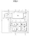
- Fig. 1 is a block diagram showing a basic configuration of Embodiment 1 of a semiconductor integrated circuit according to the invention, and a contactless IC card (a contactless electronic device) using the same.
- reference numeral 1 denotes a contactless IC card
- 2 a semiconductor integrated circuit mounted on the contactless IC card 1
- L1 an antenna mounted on the contactless IC card 1.
- the antenna L1 and a capacitor CA connected therewith in parallel make up a resonance circuit.
- the capacitor CA is not necessarily connected because adjustment is made by taking into account parasitic capacitance, and so forth.
- the semiconductor integrated circuit 2 includes a power supply circuit (PSC) 3 having power supply terminals PA, and PB, an internal circuit 4, and antenna terminals LA, and LB for connecting the antenna L1 therewith.
- PSC power supply circuit
- Fig. 2 shows a structure of the contactless IC 1.
- the contactless IC 1 is formed in the shape of a card by a printed wiring board 10 that is resin-molded.
- the antenna L1 for receiving electromagnetic waves from an interrogator 13 externally located is made up of a spiral coil 11 formed of a metal interconnection of the printed wiring board 10.
- the semiconductor integrated circuit 2 is formed as an IC chip 12 on one piece of semiconductor substrate made of material such as monocrystal silicon by the known technology for manufacturing a semiconductor integrated circuit although a method for manufacturing the same is not particularly limited thereto.
- one piece of the IC chip 12 that is the semiconductor integrated circuit 2 is mounted on the printed wiring board 10, and the coil 11 to serve as the antenna L1 is connected to the IC chip 12.
- the antenna L1 having received the electromagnetic waves from the interrogator 13 outputs a high frequency AC signal to the antenna terminals LA, and LB, respectively.
- the AC signal has been modulated by an information signal (data) during a specified time period.
- the present invention is typically applied to the contactless IC card that is a contactless electronic device, having no terminal on the surface thereof, for input from, or output to the outside, however, the present invention is obviously applicable to a dual type IC card having terminals for input and output, besides a contactless interface.
- the IC chip 12 that is the semiconductor integrated circuit 2 is formed on one piece of the semiconductor substrate made of the material such as monocrystal silicon by the known technology for manufacturing a semiconductor integrated circuit although a method for manufacturing the same is not particularly limited thereto.
- the power supply circuit 3 is made up of a rectifier and a smoothing capacitor. Needless to say, the power supply circuit 3 may be provided with a regulator function for controlling an output voltage VDD thereof so as not to exceed a predetermined voltage level.
- the internal circuit 4 includes a receiver (RU) 5, a transmitter (TU) 6, a controller (CTR) 7, a memory (MEM) 8, and a charge pump circuit (CPC) 9.
- the receiver 5 demodulates the information signal superimposed on the AC signal received by the antenna L1 provided on the contactless IC card 1, and supplies the controller 7 with a receive signal that is the digital information signal as obtained.
- the transmitter 6 receives a transmit signal that is the digital information signal outputted from the controller 7 to thereby modulate the AC signal received by the antenna L1 with the transmit signal.
- the interrogator 13 detects variation in reflection of the electromagnetic waves from the antenna L1, thereby receiving the transmit signal sent out from the controller 7.
- the memory 8 is utilized for recording and so forth of demodulated information data and transmission data, relating to controller 7.
- the charge pump circuit 9 generates a negative voltage and a high voltage from the power supply voltage.
- the high voltage generated is used for recording and so forth of, for example, data by the memory 8, however, there is no particular limitation to application purposes thereof.
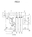
- Fig. 3 is a circuit diagram showing an example of the charge pump circuit 9 mounted on the semiconductor integrated circuit according to the present embodiment.
- the charge pump circuit 9 includes n-stages of the charge pump circuit unit cells (charge/discharge circuits) 15a, 15b, 15c, 15d, and a unidirectional element D2, and a clock signal CLK, or a clock signal CLKB corresponding to the clock signal CLK as inverted, outputted from a clock generation circuit 16, is fed to respective clock input terminals CLKIN of all the charge pump circuit unit cells 15.
- the charge pump circuit unit cells 15 each include an inverter having a PMOS (Metal Oxide Semiconductor) transistor M1, and an NMOS transistor M2, and a PMOS transistor M3 having a gate terminal to which a control terminal CTRL is connected.
- the transistor M3, and the inverter are connected in series between the one power supply terminal PA and the other power supply terminal PB.
- the inverter drives a capacitor C1 coupled between a charge output terminal QOUT of the charge pump circuit unit cell 15 and an output terminal of the inverter by the agency of the clock signal fed to the clock input terminal CLKIN. In this case, the clock signal is fed from the clock generation circuit 16 to the clock input terminal CLKIN. Further, a unidirectional element D1 is inserted between a charge input terminal QIN of the charge pump circuit unit cell 15 and the charge output terminal QOUT thereof.
- the unidirectional elements D1, D2 are each made up of a diode, however, there is no limitation thereto, and the unidirectional elements D1, D2 each may be made up of, for example, a MOS transistor a gate voltage of which is controlled by a gate voltage controlled circuit to thereby execute an on/off action. Further, with series-connection between the transistor M1 and the transistor M3, the transistor M1 may be connected to a side of the power supply, while the transistor M3 may be connected to a side of the transistor M2.
- An output signal S1 of a voltage detector 18 made up of an operational amplifier 17 and resistors R1, R2 is inputted to the control terminal CTRL of the charge pump circuit unit cell 15.
- the output signal S1 is a voltage signal outputted according to an output voltage Vout of the charge pump circuit 9 after comparing a voltage obtained by dividing the output voltage Vout at an output terminal VPP of the charge pump circuit 9 by use of the resistors R1, R2 with a reference voltage V1.
- the transistor M1 In the case of the clock input terminal CLKIN being at "L”, the transistor M1 is turned ON, and the transistor M2 is turned OFF, so that current I1 flows via the transistors M3, M1 to thereby charge the capacitor C1. At this point in time, charge is supplied from the charge input terminal QIN via the unidirectional element D1. In the case of the clock input terminal CLKIN being at "H”, the transistor M1 is turned OFF, and the transistor M2 is turned ON, so that current 12 flows via the transistor M2 to thereby discharge the capacitor C1. As the unidirectional element D1 is in the OFF state at this point in time, charge is outputted from the charge output terminal QOUT to the charge pump circuit unit cell in a succeeding stage.
- the inverter and the transistor M3 function as a switching circuit for executing a switching action to couple one of terminals of the capacitor C1 to the power supply terminal PA via the transistors M3, or to connect the same to the power supply terminal PB.
- the clock signals fed to the charge pump circuit unit cells in a preceding stage and a stage succeeding thereto, respectively, are the clock signal CLK, and the clock signal CLKB, respectively, inverted in phase from each other, so that if a charge action is executed in the preceding stage, a discharge action is executed in the stage succeeding thereto, and conversely, if the discharge action is executed in the preceding stage, the charge action is executed in the stage succeeding thereto.
- the output signal S1 undergoes a change according to a voltage level at the output terminal VPP
- the current flowing through the transistor M3 undergoes a change upon input of the output signal S1 to the control terminal CTRL.
- the current flowing through the transistor M3 is controlled so as to be decreased upon the output voltage Vout reaching a predetermined voltage level.
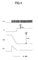
- Fig. 4 there is shown an example of operating waveforms of the charge pump circuit 9 shown in Fig. 3.
- the above-described action is repeated every time the clock signal CLK is fed to the charge pump circuit 9, thereby causing the output voltage Vout to fall.
- the output signal S1 of the voltage detector 18 keeps outputting at a ground voltage level until the output voltage Vout of the charge pump circuit 9 reaches the predetermined voltage level.
- the transistor M3 of the charge pump circuit unit cell 15, the transistor M3 being of a P-channel type is turned ON, whereupon the charge pump circuit 9 causes the output voltage thereof to fall at the maximum capacity.
- the output signal S1 of the voltage detector 18 rises in level, thereby providing feedback such that there occurs a decrease in a gate-to-source voltage Vgsp of the P-channel transistor M3 of the charge pump circuit unit cell 15. Consequently, the current flowing through the transistor M3 is decreased, thereby checking the current I1 for charging the capacitor C1. As a result, charge outputted from the charge pump circuit 9 via the unidirectional element D2 is checked, so that the output voltage Vout of the charge pump circuit 9 is maintained at the predetermined voltage level.
- the output voltage Vout of the charge pump circuit 9 can be maintained at the predetermined voltage level because the current flowing through the transistor M3 of the charge pump circuit unit cell 15 is controlled as a result of the above-described action. Consequently, the charge pump circuit 9 is prevented from making an intermittent action, so that current consumption ICP of the charge pump circuit 9 will not undergo intermittent variation. Further, since control of the output voltage Vout of the charge pump circuit 9 is effected to the gate of the transistor M3, it is possible to lower a drive capacity of the operational amplifier 17 , and accordingly, a circuit low in power consumption can be adopted for the operational amplifier 17, thereby enabling power consumption of the charge pump circuit 9 to be reduced.
- Fig. 5 is a circuit diagram showing another configuration of a charge pump circuit 9 mounted on a semiconductor integrated circuit according to Embodiment 2 of the invention.
- the charge pump circuit 9 includes N-stages of charge pump circuit unit cells 19a, 19b, 19c, 19d, and a unidirectional element D4, and a clock signal CLK, or a clock signal CLKB corresponding to the clock signal CLK as inverted, outputted from a clock generation circuit 16, is fed to respective clock input terminals CLKIN of all the charge pump circuit unit cells 19.
- the charge pump circuit unit cells 19 each include an inverter made up of a PMOS (Metal Oxide Semiconductor) transistor M4, and an NMOS transistor M5, and an NMOS transistor M6 having a gate terminal to which a control terminal CTRL is connected.
- the transistor M6, and the inverter are connected in series between the one power supply terminal PA and the other power supply terminal PB.
- the inverter drives a capacitor C2 coupled between a charge output terminal QOUT of the charge pump circuit unit cell 19 and an output terminal of the inverter by the agency of the clock signal fed to the clock input terminal CLKIN.
- the clock signal is fed from a clock generation circuit 16 to the clock input terminal CLKIN.
- a unidirectional element D3 is inserted between a charge input terminal QIN of the charge pump circuit unit cell 19 and the charge output terminal QOUT thereof.
- the unidirectional elements D3, D4 are each made up of a diode, however, there is no limitation thereto, and the unidirectional elements D3, D4 each may be made up of, for example, a MOS transistor a gate voltage which is controlled by a gate voltage controlled circuit to thereby execute an on/off action. Further, with series-connection between the transistor M5 and the transistor M6, the transistor M5 may be connected to a side of the ground, while the transistor M6 may be connected to a side of the transistor M4.
- An output signal S2 of the voltage detector 21 made up of an operational amplifier 20 and resistors R3, R4 is fed to the control terminal CTRL of the charge pump circuit unit cell 19.
- the output signal S2 is a voltage signal outputted according to an output voltage Vout of the charge pump circuit 9 after comparing a voltage obtained by dividing the output voltage Vout of the charge pump circuit 9 by use of the resistors R3 and R4 with a reference voltage V2.
- the transistor M4 In the case of the clock input terminal CLKIN being at "L”, the transistor M4 is turned ON, and the transistor M5 is turned OFF, so that current I3 flows via the transistor M4 to thereby charge the capacitor C2. At this point in time, charge is supplied from the charge input terminal QIN via the unidirectional element D3. In the case of the clock input terminal CLKIN being at "H”, the transistor M4 is turned OFF, and the transistor M5 is turned ON, so that current I4 flows via the transistors M5, M6 to thereby discharge the capacitor C2. As the unidirectional element D3 is in the OFF state at this point in time, charge is outputted from the charge output terminal QOUT to the charge pump circuit unit cell 19 in a succeeding stage.
- the inverter and the transistor M6 function as a switching circuit for executing a switching action to connect one of terminals of the capacitor C2 to the power supply terminal PA, or to couple the same to the power supply terminal PB via the transistors M6.
- the clock signals fed to the charge pump circuit unit cells in a preceding stage, and a stage succeeding thereto, respectively, are a clock signal CLK and a clock signal CLKB, respectively, inverted in phase from each other, so that if a charge action is executed in the preceding stage, a discharge action is executed in the stage succeeding thereto, and conversely, if the discharge action is executed in the preceding stage, the charge action is executed in the stage succeeding thereto.
- the output signal S2 undergoes a change according to a voltage level at the output terminal VPP, so that current flowing through the transistor M6 undergoes a change upon input of the output signal S2 to the control terminal CTRL.
- the current flowing through the transistor M6 is controlled so as to be decreased upon the output voltage Vout reaching a predetermined voltage level.
- Fig. 6 there is shown a sample of operating waveforms of the charge pump circuit 9 shown in Fig. 5.
- the above-described action is repeated every time the clock signal CLK is fed to the charge pump circuit 9, thereby causing the output voltage Vout to fall.
- the output signal S2 of the voltage detector 21 keeps outputting at a level of the power supply voltage until the output voltage Vout of the charge pump circuit 9 reaches the predetermined voltage level.
- the transistor M6 of the charge pump circuit unit cell 19 the transistor M6 being of a N-channel type, is turned ON, and the charge pump circuit 9 causes the output voltage thereof to fall at the maximum capacity.
- the output signal S2 of the voltage detector 21 falls in level, thereby providing feedback such that there occurs a decrease in a gate-to-source voltage Vgsn of the N-channel transistor M6 of the charge pump circuit unit cell 19. Consequently, the current flowing through the transistor M6 is decreased, thereby checking the current 14 for discharging the capacitor C2. As a result, charge outputted from the charge pump circuit 9 via the unidirectional element D4 is checked, so that the output voltage Vout is maintained at the predetermined voltage level.
- the output voltage Vout of the charge pump circuit 9 can be maintained at the predetermined voltage level by controlling the current flowing through the transistor M6 of the charge pump circuit unit cell 19 through the above-described action. Consequently, the charge pump circuit 9 is prevented from making an intermittent action, so that current consumption ICP of the charge pump circuit 9 will not undergo intermittent variation. Further, since control of the output voltage Vout of the charge pump circuit 9 is made against the gate of the transistor M6, it is possible to lower a drive capacity of the operational amplifier 20, and accordingly, a circuit low in power consumption can be adopted for the operational amplifier 20, thereby enabling lower power consumption of the charge pump circuit to be implemented.
- the NMOS transistor M6 for controlling charge current to the capacitor C2 can be rendered smaller in transistor size, thereby reducing a chip area.
- the charge pump circuit for generating the positive voltage is made up such that charge is provided from, for example, a ground side to thereby charge a capacitor, and subsequently, charge accumulated is released to a positive power supply side, whereupon the unidirectional element is in the OFF state, and the charge is outputted to the respective charge pump circuit unit cells, in successive stages.
Landscapes
- Engineering & Computer Science (AREA)
- Computer Hardware Design (AREA)
- Microelectronics & Electronic Packaging (AREA)
- Physics & Mathematics (AREA)
- General Physics & Mathematics (AREA)
- Theoretical Computer Science (AREA)
- Computer Networks & Wireless Communication (AREA)
- Power Engineering (AREA)
- Dc-Dc Converters (AREA)
- Semiconductor Integrated Circuits (AREA)
Abstract
Description
- The present invention relates to a power supply circuit technology suitable for application to a semiconductor integrated circuit, and in particular, to a semiconductor integrated circuit with a charge pump circuit mounted thereon, the charge pump circuit being a circuit for generating a power supplyvoltage from electromagnetic waves received by an antenna to thereby generate a high voltage from the power supply voltage, and a contactless electronic device using the semiconductor integrated circuit.
- In a charge pump circuit, boosting/lowering of voltage is generally executed by charging a capacitor through switching. In Patent Document 1 (
Japanese Patent Laid-open 2000-262043 - Further, in Patent Document 2 (
Japanese Patent Laid-open 2000-166220 - A contactless electronic device (hereinafter referred to as "a contactless IC card") without a power supply such as a battery, and so forth, operating by generating power supply voltage from electromagnetic waves received through an antenna, has been putting to much use in various sectors of business such as transportation, finance, and so forth. The contactless IC card receives data transmitted from an interrogator by modulating the electromagnetic waves, and further, executes signal processing on the data as received to thereby obtain transmit data. The contactless IC card causes a load between terminals of the antenna to change according to the transmit data as obtained. As a result, the electromagnetic waves received by the antenna are modulated by the transmit data to be then transmitted to the interrogator. The interrogator receives the transmit data by detecting variation in reflection of the electromagnetic waves as transmitted.
- Further, as the contactless IC card needs to have functions including a function for holding data as necessary, a nonvolatile memory such as an EEPROM (Electrically Erasable and Programmable ROM) is mounted thereon.
- For example, as the EEPROM makes use of a high voltage for erasing and writing data, the EEPROM requires a charge pump circuit for generating a high voltage from a power supply voltage as supplied. In this connection, in order to ensure sufficient data-maintain properties of the EEPROM, it is necessary to maintain an output voltage of the charge pump circuit at a predetermined voltage level. Further, the charge pump circuit needs to be operable at low power consumption so that the same can be operated by limited power generated from the electromagnetic waves as received. In addition, the charge pump circuit needs to be suitable for semiconductor integration.
- Next, as described above, with the contactless IC card, the data is transmitted to the interrogator by causing current flowing in the antenna to undergo a change. If the charge pump circuit repeats an intermittent action at this point in time by executing the feeding/stopping of the booster clock signal in order to keep the power supply voltage at a given level, as described in the
Patent Document 2, this will cause current consumption in the charge pump circuit to undergo variation accompanying an intermittent cycle. - Consequently, if the intermittent cycle of the charge pump circuit falls within a frequency range detectable by the interrogator, and current variation is greater in magnitude than that detectable by the interrogator, this will cause the interrogator to erroneously recognize the current consumption in the charge pump circuit as the data transmitted from the contactless IC card.
- The constant voltage circuit described in the Patent Document 1 has features in that since a voltage is kept constant by feedback (autonomous adjusting), the intermittent action can be avoided, and a component having difficulty with integration, such as a Zener diode, can be dispensed with. However, on the other hand, because all the power supply voltage of the inverter is supplied from the boosted voltage controller, there is no choice but to increase a drive capacity of the boosted voltage controller, so that an increase in power consumption is unavoidable.
- It is therefore an object of the invention to provide a semiconductor integrated circuit provided with a charge pump circuit of low power consumption, capable of maintaining an output voltage thereof at a predetermined voltage level without causing current consumption to undergo intermittent variation, and a contactless electronic device using the semiconductor integrated circuit.
- A representative embodiment of the invention disclosed in the present application is broadly and simply described as follows. More specifically, the invention provides a semiconductor integrated circuit, and a contactless electronic device using the same, the semiconductor integrated circuit including a power supply circuit for generating a DC voltage by rectifying and smoothing an AC signal supplied from an antenna, a charge pump circuit operated by the DC voltage generated by the power supply circuit, and a voltage detector for outputting a voltage according to an output voltage of the charge pump circuit, wherein the charge pump circuit may have a plural charge/discharge circuits successively connected to each other by connecting respective output terminals thereof in preceding stages with respective input terminals thereof in succeeding stages, the plurality of the charge/discharge circuits each may have a capacitor, thereby executing charge/discharge to or from the capacitor, and a charge current/discharge current flowing to or from the capacitor which is controlled according to an output voltage of the voltage detector, and thereby the output voltage of the charge pump circuit is maintained at a predetermined voltage. Because feedback is provided by control of the output voltage of the voltage detector, the semiconductor integrated circuit can maintain its output voltage constant without undergoing an intermittent action. Further, since of the capacitor is executed from the power supply circuit, and charge current/discharge current, flowing to, or from the capacitor, is controlled according to the output voltage of the voltage detector, it is possible to lighten a load on the voltage detector, thereby enabling the voltage detector to be lower in power consumption.
- Thus, with the invention, the output voltage of the charge pump circuit can be maintained at the predetermined voltage without causing current consumption of the charge pump circuit to undergo intermittent variation, thereby enabling power consumption to be kept low.
- These and other objects and many of the attendant advantages of the invention will be readily appreciated as the same becomes better understood by reference to the following detailed description when considered in connection with the accompanying drawings.
-
- Fig. 1 is a block diagram for describing Embodiment 1 of a semiconductor integrated circuit according to the invention, and a contactless electronic device using the same;
- Fig. 2 is a perspective view showing the contactless electronic device according to the invention;
- Fig. 3 is a circuit diagram showing an example of a charge pump circuit mounted on the semiconductor integrated circuit according to Embodiment 1;
- Fig. 4 is a view showing an example of operating waveforms of the charge pump circuit shown in Fig. 3;
- Fig. 5 is a circuit diagram of a charge pump circuit, for describing
Embodiment 2 of a semiconductor integrated circuit according to the invention; and - Fig. 6 is a view showing an example of operating waveforms of the charge pump circuit shown in Fig. 5.
- Embodiments of a semiconductor integrated circuit according to the invention, and a contactless electronic device using the same are described in more detail hereinafter with reference to the accompanying drawings.
- Fig. 1 is a block diagram showing a basic configuration of Embodiment 1 of a semiconductor integrated circuit according to the invention, and a contactless IC card (a contactless electronic device) using the same.
- In Fig. 1, reference numeral 1 denotes a contactless IC card, 2 a semiconductor integrated circuit mounted on the contactless IC card 1, and L1 an antenna mounted on the contactless IC card 1. The antenna L1 and a capacitor CA connected therewith in parallel make up a resonance circuit. The capacitor CA is not necessarily connected because adjustment is made by taking into account parasitic capacitance, and so forth. The semiconductor integrated
circuit 2 includes a power supply circuit (PSC) 3 having power supply terminals PA, and PB, aninternal circuit 4, and antenna terminals LA, and LB for connecting the antenna L1 therewith. - Fig. 2 shows a structure of the contactless IC 1. The contactless IC 1 is formed in the shape of a card by a printed
wiring board 10 that is resin-molded. The antenna L1 for receiving electromagnetic waves from aninterrogator 13 externally located is made up of aspiral coil 11 formed of a metal interconnection of the printedwiring board 10. The semiconductor integratedcircuit 2 is formed as anIC chip 12 on one piece of semiconductor substrate made of material such as monocrystal silicon by the known technology for manufacturing a semiconductor integrated circuit although a method for manufacturing the same is not particularly limited thereto. Thus, one piece of theIC chip 12 that is the semiconductor integratedcircuit 2 is mounted on the printedwiring board 10, and thecoil 11 to serve as the antenna L1 is connected to theIC chip 12. - The antenna L1 having received the electromagnetic waves from the
interrogator 13 outputs a high frequency AC signal to the antenna terminals LA, and LB, respectively. The AC signal has been modulated by an information signal (data) during a specified time period. - The present invention is typically applied to the contactless IC card that is a contactless electronic device, having no terminal on the surface thereof, for input from, or output to the outside, however, the present invention is obviously applicable to a dual type IC card having terminals for input and output, besides a contactless interface.
- Further, the
IC chip 12 that is the semiconductor integratedcircuit 2 is formed on one piece of the semiconductor substrate made of the material such as monocrystal silicon by the known technology for manufacturing a semiconductor integrated circuit although a method for manufacturing the same is not particularly limited thereto. - In Fig. 1, the
power supply circuit 3 is made up of a rectifier and a smoothing capacitor. Needless to say, thepower supply circuit 3 may be provided with a regulator function for controlling an output voltage VDD thereof so as not to exceed a predetermined voltage level. - The voltage VDD outputted by the
power supply circuit 3 from the power supply terminals thereof, PA, and PB, respectively, is fed to theinternal circuit 4 as a power supply voltage thereof, VDD. Theinternal circuit 4 includes a receiver (RU) 5, a transmitter (TU) 6, a controller (CTR) 7, a memory (MEM) 8, and a charge pump circuit (CPC) 9. Thereceiver 5 demodulates the information signal superimposed on the AC signal received by the antenna L1 provided on the contactless IC card 1, and supplies thecontroller 7 with a receive signal that is the digital information signal as obtained. - The
transmitter 6 receives a transmit signal that is the digital information signal outputted from thecontroller 7 to thereby modulate the AC signal received by the antenna L1 with the transmit signal. Theinterrogator 13 detects variation in reflection of the electromagnetic waves from the antenna L1, thereby receiving the transmit signal sent out from thecontroller 7. - The
memory 8 is utilized for recording and so forth of demodulated information data and transmission data, relating tocontroller 7. Thecharge pump circuit 9 generates a negative voltage and a high voltage from the power supply voltage. The high voltage generated is used for recording and so forth of, for example, data by thememory 8, however, there is no particular limitation to application purposes thereof. - Fig. 3 is a circuit diagram showing an example of the
charge pump circuit 9 mounted on the semiconductor integrated circuit according to the present embodiment. In Fig. 3, thecharge pump circuit 9 includes n-stages of the charge pump circuit unit cells (charge/discharge circuits) 15a, 15b, 15c, 15d, and a unidirectional element D2, and a clock signal CLK, or a clock signal CLKB corresponding to the clock signal CLK as inverted, outputted from aclock generation circuit 16, is fed to respective clock input terminals CLKIN of all the charge pump circuit unit cells 15. - The charge pump circuit unit cells 15 each include an inverter having a PMOS (Metal Oxide Semiconductor) transistor M1, and an NMOS transistor M2, and a PMOS transistor M3 having a gate terminal to which a control terminal CTRL is connected. The transistor M3, and the inverter are connected in series between the one power supply terminal PA and the other power supply terminal PB. The inverter drives a capacitor C1 coupled between a charge output terminal QOUT of the charge pump circuit unit cell 15 and an output terminal of the inverter by the agency of the clock signal fed to the clock input terminal CLKIN. In this case, the clock signal is fed from the
clock generation circuit 16 to the clock input terminal CLKIN. Further, a unidirectional element D1 is inserted between a charge input terminal QIN of the charge pump circuit unit cell 15 and the charge output terminal QOUT thereof. - In Fig. 3, the unidirectional elements D1, D2 are each made up of a diode, however, there is no limitation thereto, and the unidirectional elements D1, D2 each may be made up of, for example, a MOS transistor a gate voltage of which is controlled by a gate voltage controlled circuit to thereby execute an on/off action. Further, with series-connection between the transistor M1 and the transistor M3, the transistor M1 may be connected to a side of the power supply, while the transistor M3 may be connected to a side of the transistor M2.
- An output signal S1 of a
voltage detector 18 made up of anoperational amplifier 17 and resistors R1, R2 is inputted to the control terminal CTRL of the charge pump circuit unit cell 15. The output signal S1 is a voltage signal outputted according to an output voltage Vout of thecharge pump circuit 9 after comparing a voltage obtained by dividing the output voltage Vout at an output terminal VPP of thecharge pump circuit 9 by use of the resistors R1, R2 with a reference voltage V1. - In the case of the clock input terminal CLKIN being at "L", the transistor M1 is turned ON, and the transistor M2 is turned OFF, so that current I1 flows via the transistors M3, M1 to thereby charge the capacitor C1. At this point in time, charge is supplied from the charge input terminal QIN via the unidirectional element D1. In the case of the clock input terminal CLKIN being at "H", the transistor M1 is turned OFF, and the transistor M2 is turned ON, so that current 12 flows via the transistor M2 to thereby discharge the capacitor C1. As the unidirectional element D1 is in the OFF state at this point in time, charge is outputted from the charge output terminal QOUT to the charge pump circuit unit cell in a succeeding stage. Thus, the inverter and the transistor M3 function as a switching circuit for executing a switching action to couple one of terminals of the capacitor C1 to the power supply terminal PA via the transistors M3, or to connect the same to the power supply terminal PB.
- Since the clock signal is fed to the clock input terminal CLKIN, the above-described action is repeated, and supply of the charge to the charge pump circuit unit cells in respective succeeding stages is continued. The clock signals fed to the charge pump circuit unit cells in a preceding stage and a stage succeeding thereto, respectively, are the clock signal CLK, and the clock signal CLKB, respectively, inverted in phase from each other, so that if a charge action is executed in the preceding stage, a discharge action is executed in the stage succeeding thereto, and conversely, if the discharge action is executed in the preceding stage, the charge action is executed in the stage succeeding thereto. By so doing, while charge supplied to the capacitor C1 is added up backward in the n-stages of the charge pump circuit unit cells, ultimate charge is supplied to the output terminal VPP via the unidirectional element D2, thereby enabling a negative voltage to be generated.
- Meanwhile, because the output signal S1 undergoes a change according to a voltage level at the output terminal VPP, the current flowing through the transistor M3 undergoes a change upon input of the output signal S1 to the control terminal CTRL. The current flowing through the transistor M3 is controlled so as to be decreased upon the output voltage Vout reaching a predetermined voltage level. By so doing, charge to be stored in the capacitor C1 is checked, so that charge to be outputted to the succeeding stage can be checked.
- In Fig. 4, there is shown an example of operating waveforms of the
charge pump circuit 9 shown in Fig. 3. As shown Fig. 4, the above-described action is repeated every time the clock signal CLK is fed to thecharge pump circuit 9, thereby causing the output voltage Vout to fall. The output signal S1 of thevoltage detector 18 keeps outputting at a ground voltage level until the output voltage Vout of thecharge pump circuit 9 reaches the predetermined voltage level. As a result, the transistor M3 of the charge pump circuit unit cell 15, the transistor M3 being of a P-channel type, is turned ON, whereupon thecharge pump circuit 9 causes the output voltage thereof to fall at the maximum capacity. - Thereafter, upon the output voltage Vout of the
charge pump circuit 9 reaching the predetermined voltage level, the output signal S1 of thevoltage detector 18 rises in level, thereby providing feedback such that there occurs a decrease in a gate-to-source voltage Vgsp of the P-channel transistor M3 of the charge pump circuit unit cell 15. Consequently, the current flowing through the transistor M3 is decreased, thereby checking the current I1 for charging the capacitor C1. As a result, charge outputted from thecharge pump circuit 9 via the unidirectional element D2 is checked, so that the output voltage Vout of thecharge pump circuit 9 is maintained at the predetermined voltage level. - The output voltage Vout of the
charge pump circuit 9 can be maintained at the predetermined voltage level because the current flowing through the transistor M3 of the charge pump circuit unit cell 15 is controlled as a result of the above-described action. Consequently, thecharge pump circuit 9 is prevented from making an intermittent action, so that current consumption ICP of thecharge pump circuit 9 will not undergo intermittent variation. Further, since control of the output voltage Vout of thecharge pump circuit 9 is effected to the gate of the transistor M3, it is possible to lower a drive capacity of theoperational amplifier 17 , and accordingly, a circuit low in power consumption can be adopted for theoperational amplifier 17, thereby enabling power consumption of thecharge pump circuit 9 to be reduced. - Fig. 5 is a circuit diagram showing another configuration of a
charge pump circuit 9 mounted on a semiconductor integrated circuit according toEmbodiment 2 of the invention. In Fig. 5, thecharge pump circuit 9 includes N-stages of charge pumpcircuit unit cells clock generation circuit 16, is fed to respective clock input terminals CLKIN of all the charge pump circuit unit cells 19. - The charge pump circuit unit cells 19 each include an inverter made up of a PMOS (Metal Oxide Semiconductor) transistor M4, and an NMOS transistor M5, and an NMOS transistor M6 having a gate terminal to which a control terminal CTRL is connected. The transistor M6, and the inverter are connected in series between the one power supply terminal PA and the other power supply terminal PB. The inverter drives a capacitor C2 coupled between a charge output terminal QOUT of the charge pump circuit unit cell 19 and an output terminal of the inverter by the agency of the clock signal fed to the clock input terminal CLKIN. In this case, the clock signal is fed from a
clock generation circuit 16 to the clock input terminal CLKIN. Further, a unidirectional element D3 is inserted between a charge input terminal QIN of the charge pump circuit unit cell 19 and the charge output terminal QOUT thereof. - Now, in Fig. 5, the unidirectional elements D3, D4 are each made up of a diode, however, there is no limitation thereto, and the unidirectional elements D3, D4 each may be made up of, for example, a MOS transistor a gate voltage which is controlled by a gate voltage controlled circuit to thereby execute an on/off action. Further, with series-connection between the transistor M5 and the transistor M6, the transistor M5 may be connected to a side of the ground, while the transistor M6 may be connected to a side of the transistor M4.
- An output signal S2 of the
voltage detector 21 made up of anoperational amplifier 20 and resistors R3, R4 is fed to the control terminal CTRL of the charge pump circuit unit cell 19. The output signal S2 is a voltage signal outputted according to an output voltage Vout of thecharge pump circuit 9 after comparing a voltage obtained by dividing the output voltage Vout of thecharge pump circuit 9 by use of the resistors R3 and R4 with a reference voltage V2. - In the case of the clock input terminal CLKIN being at "L", the transistor M4 is turned ON, and the transistor M5 is turned OFF, so that current I3 flows via the transistor M4 to thereby charge the capacitor C2. At this point in time, charge is supplied from the charge input terminal QIN via the unidirectional element D3. In the case of the clock input terminal CLKIN being at "H", the transistor M4 is turned OFF, and the transistor M5 is turned ON, so that current I4 flows via the transistors M5, M6 to thereby discharge the capacitor C2. As the unidirectional element D3 is in the OFF state at this point in time, charge is outputted from the charge output terminal QOUT to the charge pump circuit unit cell 19 in a succeeding stage. Thus, the inverter and the transistor M6 function as a switching circuit for executing a switching action to connect one of terminals of the capacitor C2 to the power supply terminal PA, or to couple the same to the power supply terminal PB via the transistors M6.
- Since the clock signal is fed to the clock input terminal CLKIN, the above-described action is repeated, and supply of the charge to the charge pump circuit unit cells in respective succeeding stages is continued. The clock signals fed to the charge pump circuit unit cells in a preceding stage, and a stage succeeding thereto, respectively, are a clock signal CLK and a clock signal CLKB, respectively, inverted in phase from each other, so that if a charge action is executed in the preceding stage, a discharge action is executed in the stage succeeding thereto, and conversely, if the discharge action is executed in the preceding stage, the charge action is executed in the stage succeeding thereto. By so doing, while charge supplied to the capacitor C2 is added up backward in N-stages of the charge pump circuit unit cells, ultimate charge is supplied to the output terminal VPP via the unidirectional element D4, thereby enabling a negative voltage to be generated.
- As described above, the output signal S2 undergoes a change according to a voltage level at the output terminal VPP, so that current flowing through the transistor M6 undergoes a change upon input of the output signal S2 to the control terminal CTRL. The current flowing through the transistor M6 is controlled so as to be decreased upon the output voltage Vout reaching a predetermined voltage level. By so doing, charge to be stored in the capacitor C2 is checked, so that charge to be outputted to the succeeding stage can be checked.
- In Fig. 6, there is shown a sample of operating waveforms of the
charge pump circuit 9 shown in Fig. 5. As shown Fig. 6, the above-described action is repeated every time the clock signal CLK is fed to thecharge pump circuit 9, thereby causing the output voltage Vout to fall. The output signal S2 of thevoltage detector 21 keeps outputting at a level of the power supply voltage until the output voltage Vout of thecharge pump circuit 9 reaches the predetermined voltage level. As a result, the transistor M6 of the charge pump circuit unit cell 19, the transistor M6 being of a N-channel type, is turned ON, and thecharge pump circuit 9 causes the output voltage thereof to fall at the maximum capacity. - Thereafter, upon the output voltage Vout of the
charge pump circuit 9 reaching the predetermined voltage level, the output signal S2 of thevoltage detector 21 falls in level, thereby providing feedback such that there occurs a decrease in a gate-to-source voltage Vgsn of the N-channel transistor M6 of the charge pump circuit unit cell 19. Consequently, the current flowing through the transistor M6 is decreased, thereby checking the current 14 for discharging the capacitor C2. As a result, charge outputted from thecharge pump circuit 9 via the unidirectional element D4 is checked, so that the output voltage Vout is maintained at the predetermined voltage level. - The output voltage Vout of the
charge pump circuit 9 can be maintained at the predetermined voltage level by controlling the current flowing through the transistor M6 of the charge pump circuit unit cell 19 through the above-described action. Consequently, thecharge pump circuit 9 is prevented from making an intermittent action, so that current consumption ICP of thecharge pump circuit 9 will not undergo intermittent variation. Further, since control of the output voltage Vout of thecharge pump circuit 9 is made against the gate of the transistor M6, it is possible to lower a drive capacity of theoperational amplifier 20, and accordingly, a circuit low in power consumption can be adopted for theoperational amplifier 20, thereby enabling lower power consumption of the charge pump circuit to be implemented. - In this case, as the NMOS transistor is greater in mobility than the PMOS transistor, the NMOS transistor M6 for controlling charge current to the capacitor C2 can be rendered smaller in transistor size, thereby reducing a chip area.
- Having specifically described the invention with reference to the embodiments as described above, it is to be understood that the invention is not limited to those embodiments, and that obviously various changes and modifications may be made in the invention without departing from the spirit and scope thereof. For example, the charge pump circuits shown in Fig. 3, and Fig. 5, respectively, are made up so as to produce the negative voltage, however, with a charge pump circuit for generating a positive voltage, control can be similarly implemented. The charge pump circuit for generating the positive voltage is made up such that charge is provided from, for example, a ground side to thereby charge a capacitor, and subsequently, charge accumulated is released to a positive power supply side, whereupon the unidirectional element is in the OFF state, and the charge is outputted to the respective charge pump circuit unit cells, in successive stages.
- Features, components and specific details of the structures of the above-described embodiments may be exchanged or combined to form further embodiments optimized for the respective application. As far as those modifications are readily apparent for an expert skilled in the art they shall be disclosed implicitly by the above description without specifying explicitly every possible combination, for the sake of conciseness of the present description.
Claims (14)
- A semiconductor integrated circuit comprising:a power supply circuit (3) for generating a DC voltage by rectifying and smoothing an AC signal supplied from an antenna (L1); a charge pump circuit (9) operated by the DC voltage generated bythe power supply circuit (3); anda voltage detector (18, 21) for outputting a voltage according to an output voltage of the charge pump circuit (9),wherein the charge pump circuit (9) includes a plurality of charge/discharge circuits (15, 19) successively connected to each other by connecting respective output terminals (QOUT) thereof in preceding stages with respective input terminals (QIN) thereof in succeeding stages,
the plurality of the charge/discharge circuits (15, 19) each has a capacitor (C1, C2), thereby executing charge/discharge to or from the capacitor (C1, C2), and
a charge current/discharge current flowing to or from the capacitor (C1, C2) is controlled according to an output voltage (VOUT) of the voltage detector (18, 21), and thereby the output voltage (VOUT) of the charge pump circuit (9) is maintained at a predetermined voltage. - The semiconductor integrated circuit according to claim 1, wherein
each of the plurality of the charge/discharge circuits (15, 19) is made up such that an inverter and a MOS transistor are connected in series between power supply terminals (PA, PB) of the power supply circuit (3), the capacitor (C1, C2) is coupled between an output terminal of the inverter, and an output terminal of each of the plurality of the charge/discharge circuits (15, 19), and further a unidirectional element (D1, D3) is connected between an input terminal (QIN) of each of the plurality of the charge/discharge circuits (15, 19) and the output terminal (QOUT) thereof, and
the output voltage (VOUT) of the voltage detector (18, 21) being inputted to a gate terminal of the MOS transistor. - The semiconductor integrated circuit according to claim 1 or 2, wherein
a clock signal (CLK) is fed to an input terminal (CLKIN) of the inverter, the clock signals (CLK) fed to each of the plurality of the charge/discharge circuits (15, 19) in the preceding stage and the succeeding stage adjacent thereto, respectively, are inverted in phase from each other, and
charge/discharge to or from the capacitor (C1, C2) is executed by the inverter according to the clock signal (CLK). - A semiconductor integrated circuit comprising:an antennal terminal (LA, LB) connected to an antenna (L1);wherein the charge pump circuit (9) includes a plurality of charge/discharge circuits (15, 19) successively connected to each other by connecting respective output terminals (QOUT) thereof in preceding stages with respective input terminals (QIN) thereof in succeeding stages,a power supply circuit (3) for generating a DC voltage by rectifying and smoothing an AC signal supplied from the antenna (L1) to the antennal terminal (LA, LB);a charge pump circuit (9) operated by the DC voltage generated by the power supply circuit (3); anda voltage detector (18, 21) for outputting a voltage according to an output voltage (VOUT) of the charge pump circuit (9),
wherein each of the plurality of the charge/discharge circuits (15, 19) comprises:a capacitor (C1, C2) where charge current flows in from one of power supply terminals (PA, PB) outputting the DC voltage, and discharge current flows out to the other of the power supply terminals (PA, PB); anda switching circuit for executing charge/discharge to or from the capacitor (C1, C2) according to a clock signal (CLK), andwherein charge current/discharge current flowing to or from the capacitor (C1, C2) is controlled according to an output voltage (VOUT) of the voltage detector (18, 21), and thereby the output voltage (VOUT) of the charge pump circuit (9) is maintained at a predetermined voltage. - The semiconductor integrated circuit according to claim 4, wherein
each of the plurality of the charge/discharge circuits (15, 19) has a unidirectional element connecting an input terminal (QIN) of each of the plurality of the charge/discharge circuits (15, 19) to an output terminal (QOUT) thereof,
the switching circuit includes an inverter and a MOS transistor, connected in series between the one power supply terminal of the power supply circuit and the other power supply terminal,
the capacitor (C1, C2) is coupled between an output terminal of the inverter and an output terminal of each of the plurality of the charge/discharge circuits (15, 19),
the clock signal (CLK) is inputted to an input terminal (CLKIN) of the inverter, and
the output voltage (VOUT) of the voltage detector (18, 21) is inputted to a gate terminal of the MOS transistor. - The semiconductor integrated circuit according to claim 4 or 5, wherein the clock signals (CLK) fed to each of the plurality of the charge/discharge circuits (15, 19) in the preceding stage and the succeeding stage adjacent thereto, respectively, are inverted in phase from each other.
- The semiconductor integrated circuit according to at least one of claims 1 to 3, wherein the unidirectional element is a diode.
- The semiconductor integrated circuit according to at least one of claims 4 to 6, wherein the unidirectional element is a diode.
- The semiconductor integrated circuit according to at least one of claims 1 to 3 and 7, wherein the unidirectional element is a MOS transistor, and an on/off action of the MOS transistor is controlled by a gate voltage thereof.
- The semiconductor integrated circuit according to at least one of claims 4 to 6 and 8, wherein the unidirectional element is a MOS transistor, and an on/off action of the MOS transistor is controlled by a gate voltage thereof.
- The semiconductor integrated circuit according to at least one of claims 1 to 3, 7 and 9, wherein
the voltage detector (18, 21) comprises a first resistor (R1, R3), a second resistor (R2, R4) and an operational amplifier (17, 20),
a potential difference between an output voltage of the power supply circuit (3) and the output voltage of the charge pump circuit (9) is divided by the first resistor (R1, R3) and the second resistor (R2, R4), and
a voltage obtained by dividing the potential difference is compared with a reference voltage by the operational amplifier (17, 20) to thereby output the voltage according to the output voltage of the charge pump circuit (9). - The semiconductor integrated circuit according to at least one of claims 4 to 6, 8 and 10, wherein
the voltage detector (18, 21) comprises a first resistor (R1, R3), a second resistor (R2, R4) and an operational amplifier (17, 20),
a potential difference between an output voltage of the power supply circuit (3) and the output voltage of the charge pump circuit (9) is divided by the first resistor (R1, R3) and the second resistor (R2, R4), and
a voltage obtained by dividing the potential difference is compared with a reference voltage by the operational amplifier (17, 20) to thereby output the voltage according to the output voltage of the charge pump circuit (9). - A contactless electronic device comprising: a substrate (10);
a coil (11) formed on the substrate (10), serving as an antenna (L1); and
the semiconductor integrated circuit (12) according to claim 1, connected to the coil (11), and mounted on the substrate (10). - A contactless electronic device comprising: a substrate (10);
a coil (11) formed on the substrate (10), serving as an antenna (L1); and
the semiconductor integrated circuit (12) according to claim 4, connected to the coil (11), and mounted on the substrate (10).
Applications Claiming Priority (1)
| Application Number | Priority Date | Filing Date | Title |
|---|---|---|---|
| JP2005312220A JP4750530B2 (en) | 2005-10-27 | 2005-10-27 | Semiconductor integrated circuit device and non-contact electronic device using the same |
Publications (3)
| Publication Number | Publication Date |
|---|---|
| EP1780660A2 true EP1780660A2 (en) | 2007-05-02 |
| EP1780660A3 EP1780660A3 (en) | 2010-06-09 |
| EP1780660B1 EP1780660B1 (en) | 2011-12-14 |
Family
ID=37685225
Family Applications (1)
| Application Number | Title | Priority Date | Filing Date |
|---|---|---|---|
| EP06022553A Expired - Fee Related EP1780660B1 (en) | 2005-10-27 | 2006-10-27 | Semiconductor integrated circuit and contactless electronic device using the same |
Country Status (6)
| Country | Link |
|---|---|
| US (1) | US8200152B2 (en) |
| EP (1) | EP1780660B1 (en) |
| JP (1) | JP4750530B2 (en) |
| KR (1) | KR20070045963A (en) |
| CN (1) | CN1956289B (en) |
| TW (1) | TW200732975A (en) |
Families Citing this family (13)
| Publication number | Priority date | Publication date | Assignee | Title |
|---|---|---|---|---|
| WO2008102814A1 (en) * | 2007-02-23 | 2008-08-28 | Nec Corporation | Semiconductor device performing signal transmission by using inductor coupling |
| JP4420068B2 (en) * | 2007-05-25 | 2010-02-24 | セイコーエプソン株式会社 | Power transmission device and electronic device |
| KR100995752B1 (en) | 2008-12-24 | 2010-11-19 | 삼성에스디에스 주식회사 | Power Interface Circuit of Contact IC Card Reader |
| US20110168782A1 (en) * | 2010-01-12 | 2011-07-14 | Nxp B.V. | Capacitance under a fringe capacitor of a radio frquency integrated circuit |
| CN102238766A (en) * | 2010-04-20 | 2011-11-09 | 成都蜀昌科技有限公司 | General high-efficiency long-life driving circuit for wide voltage non-inductance semiconductor illumination |
| CA2752716C (en) * | 2010-09-21 | 2019-04-30 | Inside Secure | Nfc card sensitive to foucault currents |
| US8416010B2 (en) * | 2011-04-27 | 2013-04-09 | Intersil Americas Inc. | Adaptive charge pump |
| CN104517645B (en) * | 2014-05-16 | 2019-08-13 | 上海华虹宏力半导体制造有限公司 | Flash memory low speed reading mode control circuit |
| CN106203582B (en) * | 2015-02-11 | 2019-11-15 | 天地融科技股份有限公司 | A kind of electronic equipment |
| FR3062937A1 (en) * | 2017-02-14 | 2018-08-17 | Stmicroelectronics (Rousset) Sas | ACTIVATION OF AN NFC DEVICE |
| CN107993689A (en) * | 2017-12-13 | 2018-05-04 | 上海华虹宏力半导体制造有限公司 | A kind of voltage-dividing detection circuit for reducing power consumption |
| JP6798053B1 (en) * | 2020-02-04 | 2020-12-09 | 富士フイルム株式会社 | Non-contact communication media, magnetic tape cartridges, non-contact communication media operating methods, and programs |
| EP3930133B1 (en) * | 2020-06-25 | 2024-02-21 | Samsung Electronics Co., Ltd. | Internal voltage generation circuit of smart card and smart card including the same |
Family Cites Families (24)
| Publication number | Priority date | Publication date | Assignee | Title |
|---|---|---|---|---|
| JP3004043B2 (en) * | 1990-10-23 | 2000-01-31 | 株式会社東芝 | Nonvolatile semiconductor memory device |
| US5247241A (en) * | 1991-10-21 | 1993-09-21 | Silicon Systems, Inc. | Frequency and capacitor based constant current source |
| NL9200056A (en) * | 1992-01-14 | 1993-08-02 | Sierra Semiconductor Bv | HIGH VOLTAGE GENERATOR WITH OUTPUT CURRENT CONTROL. |
| JPH06283667A (en) | 1993-03-26 | 1994-10-07 | Toshiba Corp | High-voltage generation circuit |
| US5450027A (en) * | 1994-04-08 | 1995-09-12 | At&T Corp. | Low-power-dissipation CMOS circuits |
| JP2679617B2 (en) | 1994-04-18 | 1997-11-19 | 日本電気株式会社 | Charge pump circuit |
| KR0145615B1 (en) | 1995-03-13 | 1998-12-01 | 김광호 | The driving device of the tft liquid crystal display |
| EP0951072B1 (en) * | 1996-04-08 | 2009-12-09 | Hitachi, Ltd. | Semiconductor integrated circuit device |
| US5708419A (en) * | 1996-07-22 | 1998-01-13 | Checkpoint Systems, Inc. | Method of wire bonding an integrated circuit to an ultraflexible substrate |
| FR2752318B1 (en) * | 1996-08-06 | 1998-09-04 | Inside Technologies | INTEGRATED CIRCUIT WITH NON-CONTACT OPERATION, COMPRISING A LOAD PUMP |
| JP3488587B2 (en) * | 1997-01-09 | 2004-01-19 | 株式会社東芝 | Boost circuit and IC card having the same |
| JP3487581B2 (en) | 1998-09-22 | 2004-01-19 | シャープ株式会社 | Power supply circuit and display device and electronic equipment using the same |
| JP2000262043A (en) | 1999-03-10 | 2000-09-22 | Nec Corp | Constant voltage circuit |
| JP3614747B2 (en) | 2000-03-07 | 2005-01-26 | Necエレクトロニクス株式会社 | BOOST CIRCUIT, IC CARD WITH THE SAME AND ELECTRONIC DEVICE WITH THE SAME |
| JP2002150250A (en) | 2000-11-16 | 2002-05-24 | Matsushita Electric Ind Co Ltd | IC chip for non-contact IC card |
| US6504422B1 (en) | 2000-11-21 | 2003-01-07 | Semtech Corporation | Charge pump with current limiting circuit |
| JP2003033007A (en) * | 2001-07-09 | 2003-01-31 | Sanyo Electric Co Ltd | Controlling method for charge pump circuit |
| US6756838B1 (en) * | 2003-03-18 | 2004-06-29 | T-Ram, Inc. | Charge pump based voltage regulator with smart power regulation |
| JP4031399B2 (en) * | 2003-07-08 | 2008-01-09 | セイコーインスツル株式会社 | Semiconductor integrated circuit device |
| US7494066B2 (en) | 2003-12-19 | 2009-02-24 | Semiconductor Energy Laboratory Co., Ltd. | Semiconductor device |
| JP2005192350A (en) * | 2003-12-26 | 2005-07-14 | Matsushita Electric Ind Co Ltd | Step-down charge pump type power supply circuit and monolithic integrated circuit |
| DE102004034768B4 (en) * | 2004-07-19 | 2007-11-15 | Infineon Technologies Ag | Identification media |
| JP4113170B2 (en) * | 2004-09-08 | 2008-07-09 | 株式会社東芝 | Semiconductor device |
| US7259612B2 (en) * | 2005-06-28 | 2007-08-21 | Atmel Corporation | Efficient charge pump for a wide range of supply voltages |
-
2005
- 2005-10-27 JP JP2005312220A patent/JP4750530B2/en not_active Expired - Fee Related
-
2006
- 2006-10-25 US US11/585,839 patent/US8200152B2/en not_active Expired - Fee Related
- 2006-10-26 KR KR1020060104539A patent/KR20070045963A/en not_active Withdrawn
- 2006-10-27 EP EP06022553A patent/EP1780660B1/en not_active Expired - Fee Related
- 2006-10-27 CN CN2006101425004A patent/CN1956289B/en not_active Expired - Fee Related
- 2006-10-27 TW TW095139906A patent/TW200732975A/en unknown
Also Published As
| Publication number | Publication date |
|---|---|
| TW200732975A (en) | 2007-09-01 |
| CN1956289B (en) | 2010-05-12 |
| US8200152B2 (en) | 2012-06-12 |
| EP1780660A3 (en) | 2010-06-09 |
| EP1780660B1 (en) | 2011-12-14 |
| KR20070045963A (en) | 2007-05-02 |
| JP2007124770A (en) | 2007-05-17 |
| CN1956289A (en) | 2007-05-02 |
| US20070097725A1 (en) | 2007-05-03 |
| JP4750530B2 (en) | 2011-08-17 |
Similar Documents
| Publication | Publication Date | Title |
|---|---|---|
| US7853236B2 (en) | Rectifier circuit and RFID tag | |
| US8344791B2 (en) | Charge pump circuits and methods | |
| EP1780660B1 (en) | Semiconductor integrated circuit and contactless electronic device using the same | |
| EP1852804B1 (en) | Rectifier circuit radio communication device | |
| US7180794B2 (en) | Oscillating circuit, booster circuit, nonvolatile memory device, and semiconductor device | |
| US6525362B2 (en) | IC chip for contactless IC card | |
| US6437609B1 (en) | Charge pump type voltage booster circuit | |
| JP4786316B2 (en) | Semiconductor integrated circuit device and IC card using the same | |
| CN106849642B (en) | Charge pump regulation | |
| US10432107B2 (en) | Rectifier circuit and electronic device | |
| US20150207404A1 (en) | Dc-dc voltage converter and conversion method | |
| JP2002247838A (en) | Booster circuit and drain-source voltage relaxation type inverter circuit | |
| US20170272060A1 (en) | Oscillation circuit, booster circuit, and semiconductor device | |
| US7834661B2 (en) | Ultra-low-power level shifter, voltage transform circuit and RFID tag including the same | |
| CN113783420A (en) | Low-power-consumption charge pump circuit for non-volatile memory in Internet of things security chip and working method | |
| EP1493223B1 (en) | Voltage converter using mos transistors | |
| US7400874B2 (en) | Integrated circuit comprising a clock-signal generator, smart card comprising an integrated circuit of this kind and associated method for the generation of clock signals | |
| US20050180227A1 (en) | Booster circuit | |
| US7023261B2 (en) | Current switching for maintaining a constant internal voltage | |
| US20110025279A1 (en) | Power supply circuit and semiconductor device | |
| US20060186943A1 (en) | Ultra-low-power voltage transform circuit | |
| US7642839B2 (en) | Current consumption prevention apparatus of a high voltage generator | |
| JPH09205348A (en) | Semiconductor device and ic card device using it | |
| WO2006038549A1 (en) | Power supply control circuit | |
| JP2008277923A (en) | Clock error detection circuit |
Legal Events
| Date | Code | Title | Description |
|---|---|---|---|
| PUAI | Public reference made under article 153(3) epc to a published international application that has entered the european phase |
Free format text: ORIGINAL CODE: 0009012 |
|
| AK | Designated contracting states |
Kind code of ref document: A2 Designated state(s): AT BE BG CH CY CZ DE DK EE ES FI FR GB GR HU IE IS IT LI LT LU LV MC NL PL PT RO SE SI SK TR |
|
| AX | Request for extension of the european patent |
Extension state: AL BA HR MK YU |
|
| PUAL | Search report despatched |
Free format text: ORIGINAL CODE: 0009013 |
|
| AK | Designated contracting states |
Kind code of ref document: A3 Designated state(s): AT BE BG CH CY CZ DE DK EE ES FI FR GB GR HU IE IS IT LI LT LU LV MC NL PL PT RO SE SI SK TR |
|
| AX | Request for extension of the european patent |
Extension state: AL BA HR MK RS |
|
| RAP1 | Party data changed (applicant data changed or rights of an application transferred) |
Owner name: RENESAS ELECTRONICS CORPORATION |
|
| 17P | Request for examination filed |
Effective date: 20101209 |
|
| AKX | Designation fees paid |
Designated state(s): DE FR NL |
|
| GRAP | Despatch of communication of intention to grant a patent |
Free format text: ORIGINAL CODE: EPIDOSNIGR1 |
|
| RIC1 | Information provided on ipc code assigned before grant |
Ipc: H02M 3/07 20060101ALI20110531BHEP Ipc: G06K 19/07 20060101AFI20110531BHEP |
|
| GRAS | Grant fee paid |
Free format text: ORIGINAL CODE: EPIDOSNIGR3 |
|
| GRAA | (expected) grant |
Free format text: ORIGINAL CODE: 0009210 |
|
| AK | Designated contracting states |
Kind code of ref document: B1 Designated state(s): DE FR NL |
|
| REG | Reference to a national code |
Ref country code: NL Ref legal event code: T3 |
|
| REG | Reference to a national code |
Ref country code: DE Ref legal event code: R096 Ref document number: 602006026332 Country of ref document: DE Effective date: 20120209 |
|
| PLBE | No opposition filed within time limit |
Free format text: ORIGINAL CODE: 0009261 |
|
| STAA | Information on the status of an ep patent application or granted ep patent |
Free format text: STATUS: NO OPPOSITION FILED WITHIN TIME LIMIT |
|
| 26N | No opposition filed |
Effective date: 20120917 |
|
| REG | Reference to a national code |
Ref country code: DE Ref legal event code: R097 Ref document number: 602006026332 Country of ref document: DE Effective date: 20120917 |
|
| PGFP | Annual fee paid to national office [announced via postgrant information from national office to epo] |
Ref country code: FR Payment date: 20121010 Year of fee payment: 7 Ref country code: DE Payment date: 20121031 Year of fee payment: 7 |
|
| PGFP | Annual fee paid to national office [announced via postgrant information from national office to epo] |
Ref country code: NL Payment date: 20121030 Year of fee payment: 7 |
|
| REG | Reference to a national code |
Ref country code: NL Ref legal event code: V1 Effective date: 20140501 |
|
| REG | Reference to a national code |
Ref country code: DE Ref legal event code: R119 Ref document number: 602006026332 Country of ref document: DE Effective date: 20140501 |
|
| REG | Reference to a national code |
Ref country code: FR Ref legal event code: ST Effective date: 20140630 |
|
| PG25 | Lapsed in a contracting state [announced via postgrant information from national office to epo] |
Ref country code: DE Free format text: LAPSE BECAUSE OF NON-PAYMENT OF DUE FEES Effective date: 20140501 Ref country code: NL Free format text: LAPSE BECAUSE OF NON-PAYMENT OF DUE FEES Effective date: 20140501 Ref country code: FR Free format text: LAPSE BECAUSE OF NON-PAYMENT OF DUE FEES Effective date: 20131031 |