EP1780559B1 - Optical sensor - Google Patents
Optical sensor Download PDFInfo
- Publication number
- EP1780559B1 EP1780559B1 EP20060022107 EP06022107A EP1780559B1 EP 1780559 B1 EP1780559 B1 EP 1780559B1 EP 20060022107 EP20060022107 EP 20060022107 EP 06022107 A EP06022107 A EP 06022107A EP 1780559 B1 EP1780559 B1 EP 1780559B1
- Authority
- EP
- European Patent Office
- Prior art keywords
- optoelectronic device
- mirror
- light beams
- transmitted light
- receiver
- Prior art date
- Legal status (The legal status is an assumption and is not a legal conclusion. Google has not performed a legal analysis and makes no representation as to the accuracy of the status listed.)
- Expired - Fee Related
Links
Images


Classifications
-
- G—PHYSICS
- G01—MEASURING; TESTING
- G01V—GEOPHYSICS; GRAVITATIONAL MEASUREMENTS; DETECTING MASSES OR OBJECTS; TAGS
- G01V8/00—Prospecting or detecting by optical means
- G01V8/10—Detecting, e.g. by using light barriers
- G01V8/12—Detecting, e.g. by using light barriers using one transmitter and one receiver
- G01V8/14—Detecting, e.g. by using light barriers using one transmitter and one receiver using reflectors
Definitions
- the invention relates to an optoelectronic device.
- An optoelectronic device of the type in question is known from DE 101 35 036 A1 known.
- the optoelectronic device described therein forms a frame light barrier with a laser diode for generating a light beam at a periodic reflection angle and first and second opposing planar mirror surfaces.
- the scanner mirror and the first and second mirror surfaces are arranged such that a generated light beam is reflected back and forth by the scanner mirror onto the first mirror surface, from there to the second mirror surface, between the first and second mirror surfaces, and then onto the light receiver.
- a device for generating a light band comprising a laser diode for generating a light beam, a scanner mirror for reflecting the light beam at a periodic reflection angle and a deflection prism for generating a substantially uniform light band on a CCD line.
- a disadvantage of this optoelectronic device is their high susceptibility to interference. This is based on the fact that the flat mirror surfaces must be aligned extremely exactly parallel to each other, so that the light rays can be guided in a desired manner along these mirror surfaces. However, even the smallest recesses of these mirror surfaces lead to a lateral escape of the light rays, so that it is no longer functional.
- a device is known from EP A 0 021 163 known.
- This device forms an anti-burglary protection for surfaces in which the edge of the surface to be protected is provided with light-reflecting layers which direct the light emanating from a light source to a receiver and in which alarm is triggered upon influencing this light.
- the light-reflecting layers are formed of elements which reflect an incident light beam independently of its angular position in the plane defined by the layers parallel to its direction of incidence. These elements are designed as mirror strips containing 90 ° angle mirrors or 90 ° orbits as reflective elements. Several such mirrors or prisms can be grouped together in a mirror bar.
- the DE 195 33 044 A1 relates to a double light barrier.
- This light barrier consists of a transmitter / receiver part and a reflector part, wherein the transmitter and the receiver are facing away from one another in a plane and the reflector part has reflective elements such that a light beam emitted by the transmitter is mirrored so that a back-plate is formed runs parallel to the emitted light beam and hits the receiver.
- the reflector part to the light barrier has an array of reflective elements such that the distance between the transmitter and the receiver is bridged and form a triple mirror, through which the received first barrier beam is reflected at a corresponding distance as a second, parallel barrier beam. If one or the other barrier beam is interrupted, the light barrier emits a switching signal.
- the DE 195 04 230 A1 relates to an optoelectronic device having a transmission element emitting a transmitting light beam and a receiving element remote from the transmitting element, on which the transmitted light beam is guided via at least one deflection unit.
- the transmitted light rays is in a level led.
- the deflecting unit has two mirror-symmetrically arranged, perpendicular to the plane, flat mirror surfaces which are arranged opposite one another at a fixed predetermined angle so that the transmitted light beam is reflected once at the mirror surfaces.
- the deflection unit is rotatable about an axis of rotation perpendicular to the plane of the transmitted light beam.
- the invention has the object of providing an optoelectronic device of the type mentioned in such a way that it has the lowest possible susceptibility to interference with high functionality.
- the optoelectronic device is used to detect objects in a surveillance area and consists of a transmit light emitting emitter, a receiving light beam receiving receiver, an evaluation unit for generating an object detection signal in response to the received signals of the receiver and two monitoring areas delimiting mirror parts.
- the transmitted light rays are guided by reflections on these mirror parts of the transmitter and receiver.
- At least one of the mirror parts has at least two mutually inclined mirror surfaces on which the transmitted light beams are deflected transversely to the direction of propagation.
- the transmitter and receiver form a distance sensor element by means of which the transit time of the transmitted light beams is determined by the monitoring area. To check the function of the optoelectronic device, the determined transit time of the transmitted light beams is compared by the monitoring area with a desired value.
- the optoelectronic device Since the transmitter and the receiver, a distance sensor, by means of which the duration of the transmitted light beams is controlled, the reliability of the optoelectronic device increases. Thus, the optoelectronic device according to the invention is also suitable for safety applications.
- a significant advantage of the invention is that stabilized by the formation of at least one of the mirror parts with mutually inclined mirror surfaces by the conditional beam guidance of the transmitted light beams transversely to the propagation direction such that the optoelectronic device is insensitive to lateral tilting of the mirror parts.
- the mirror parts of the optoelectronic device therefore do not need to be adjusted exactly transversely to the direction of propagation, which considerably facilitates the fixing and mounting of the optoelectronic device. Since the functionality of the optoelectronic device still remains intact even with lateral tilting of the mirror parts, this has a low susceptibility to interference.
- a threshold value evaluation of the received signals of the receiver preferably takes place.
- the resulting switching signal indicates whether an object is in the surveillance area or not.
- the optoelectronic device By configuring the optoelectronic device with two opposing mirror parts extending along the surveillance area, the optoelectronic device can be formed as a light grid.
- the sensor components of the optoelectronic device can also form a concentric arrangement, which is particularly suitable for the detection of small parts in pipes.
- FIG. 1 shows the block diagram of an optoelectronic device 1 with a transmitter 2, which emits transmitted light beams 3 in a region to be monitored. Furthermore, the optoelectronic device 1 comprises a receiving light beams 4 receiving receiver 5.
- the transmitter 2 is formed by a light emitting diode.
- the receiver 5 may be formed as a photodiode.
- the transmitted light beams 3 are guided between two mirror parts 7, 7 'and then guided as receiving light beams 4 to the receiver 5.
- a sensor-side mirror part 7 and a distance to this further mirror part 7 ' is provided. Due to the multiple reflection of the transmitted light beams 3 between the two mirror parts 7 and 7 ', the object 6 is reliably detected even in small dimensions in the surveillance area.
- the transmitted light beams 3 are strongly attenuated and the film is reliably detected.
- the object detection takes place in such a way that a binary switching signal is derived from the received signals present at the receiver as an object detection signal, the switching states of which indicate whether or not an object is located in the monitored area.
- the switching signal is measured by a threshold value evaluation of the received signals at the output of the receiver 5.
- the evaluation takes place in an evaluation unit 8, which is accommodated with the other components of the optoelectronic device 1 in a housing 9.
- the switching signal is output via a switching output 10, which is connected to the Evaluation unit 8 is connected.
- a parameterization interface 11 is connected to the evaluation unit 8.
- FIG. 2 shows a variant of the optoelectronic device 1 according to FIG. 1 , which operates on the principle of the light barrier, wherein the mirror part 7 between the transmitter 2 and receiver 5 is arranged.
- the mirror parts 7, 7 ' are mounted in oppositely disposed parts of the housing 9.
- a transmitting optics 19 for beam shaping of the transmitted light beams 3 and a receiving optics 20 for focusing the received light beams 4 are provided on the receiver 5. Furthermore, in this part of the housing 15, a printed circuit board 21 is integrated, on which the transmitter 2 and receiver 5 and the components of the evaluation unit 8 not shown separately are arranged.
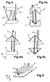
- FIG. 3 shows mirror parts 7, 7 'according to the prior art, each having flat mirror surfaces to guide the transmitted light beams 3 from the transmitter 2 via the mirror parts 7, 7' from the receiver 5. Even the slightest deviations from the parallel beam guidance lead as in FIG. 3 shown to a lateral escape of the received light beams 4, that is, these no longer reach the receiver.
- FIG. 4a shows a first embodiment of the mirror parts 7, 7 'according to the invention with surface mirrors, which are formed from two mirrors each, which are inclined by 90 ° to each other. As a result, a lateral escape of the received light beam 4 is prevented. It shows FIG. 4 the mirror parts 7, 7 'of an optoelectronic device 1 according to FIG FIG. 1 or 2 in cross section.
- FIG. 4b shows a cross-sectional view of a second embodiment of the mirror parts 7, 7 'of the optoelectronic device 1 according to FIG. 1 or 2 , wherein the sensor-side mirror part 7 is formed by a roof prism, whereby the false angle of the incident transmitted light beams 3 is not increased by the further reflections.
- the mirror part 7 ' has a flat mirror surface, which is formed by a plane mirror.
- Figure 4c shows a third embodiment, wherein both mirror parts 7, 7 'are formed by roof prisms.
- FIG. 5 shows a fourth embodiment, in which the mirror parts 7, 7 'are formed by roof prism panels.
- the advantage here is that the mirror parts 7, 7 'can be very flat.
- the propagation direction of the transmitted light beams 3 is in the X direction.
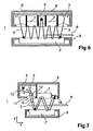
- FIG. 6 shows an extension of in FIG. 2 illustrated optoelectronic device 1 with an additional reference channel, which is not affected by an object 6.
- the reference channel is used to determine the basic attenuation of the free path, that is, the attenuation of the transmitted light beams 3 when passing through the object-free monitoring area.
- the reference channel is formed by a transmitter 2 'which emits transmitted light beams 3'.
- the transmitted light beams 3 'of the transmitter 2' are guided to the same receiver 5 as the transmitted light beams 3 of the transmitter 2, the transmitters 2, 2 'being activated alternately, so that the signals generated by the transmitters 2, 2' at the receiver 5 can be evaluated separately.
- Drift effects such as slow pollution or temperature-induced changes in angle can be compensated.
- FIG. 7 shows an embodiment of an optoelectronic device 1, which operates on the reflex and Autokollimationskal.
- the emitted light beams 3 emitted by the transmitter 2 are guided again via the mirror parts 7, 7 'within the surveillance area.
- the transmitter 2 and the receiver 5 are arranged side by side on the same side of the surveillance area. After the emitted light beams 3 emitted by the transmitter 2 are guided through the surveillance area for the first time, they meet a triple reflector 18.
- the triple light reflector 18 deflects the transmitted light beams 3 as received light beams 4.
- the received light beams 4 are like the transmitted light beams 3 passed through a common transmitting-receiving lens 17 and directed by a beam splitter 12 and a deflecting mirror 13 to the receiver 5.
- reflection light barriers can be used with polarizing filters, so that only received light beams 4 are taken into account by the triple reflector 18 and direct reflections from a mirror part 7, 7 'are suppressed.
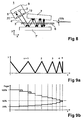
- FIG. 8 shows an embodiment of an optoelectronic device 1, in which the transmitter 2 and receiver 5 are arranged in a common housing 9.
- the transmitter 2 is assigned a transmitting optics 19
- the receiver 5 is associated with a receiving optics 20.
- the angle of incidence becomes the transmitted light beams 3 after each reflection larger.
- the transmitted light beams 3 reverse and reach the sensor as receiving light beams 4 in parallel with the transmitted light beams 3.
- FIG. 9b shows the diagram of the attenuation curve of the transmitted light beams 3 of the optoelectronic device 1 according to FIG. 8 at free range.
- the attenuation at entry and exit from the roof prism is each about 4%. If the mirror part 7 'formed by a surface plan mirror, can be expected with about 5% damping.
- Previous film sensors according to the reflection principle achieve only an attenuation to 84%, that is, taking into account tolerances, disturbances and contamination of about 10%, only about 6% remain as a functional reserve, resulting in a limited detection reliability.
- FIG. 10a - c show a variant of the optoelectronic device 1 according to FIG. 8 ,
- the optoelectronic device 1 shown in a longitudinal section differs from the optoelectronic device 1 according to FIG. 8 only with regard to the training of their mirror parts 7, 7 ', in FIG. 10b are shown in a plan view.
- the mirror parts 7, 7 'in the propagation direction of the transmitted light beams 3 is not inclined, yet with the mirror parts 7, 7' of the optoelectronic device 1 according to FIG. 10a-c a beam reversal of the transmitted light beams 3 is achieved.
- FIG. 10a a beam reversal by prismatic thickening at the beginning (area a), or tapering at the end (area c) of the mirror part 7 is reached.
- the region a ensures that the angle of incidence of the transmitted light beams 3 is reduced so that the transmitted light beams 3 are so dense in the region b that small parts are reliably detected, or clear films produce sufficient overall attenuation.
- the region c ensures that for the transmitted light beams 3, even with tolerances with respect to the alignment of the mirror parts 7, 7 'to each other, a beam reversal takes place, that is to say that the transmitted light beams 3 reverse in this area and then run as receiving light beams 4 back to the receiver 5.
- FIG. 10b shows the mirror parts 7, 7 'from the front, wherein the mirror part 7' can also be formed by a plane mirror. As can be seen from this illustration, both mirror parts 7, 7 'have a prism structure transversely to the propagation direction of the transmitted light beams 3.
- the distance d3 between the mirror parts 7, 7 'and the length of the regions a and c, the beam path of the transmitted light beams 3 and received light beams 5 is defined.
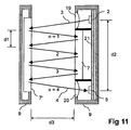
- FIG. 11 shows an embodiment of an optoelectronic device 1, which in terms of its construction of the optoelectronic device 1 according to FIG. 2 equivalent.
- the optoelectronic device 1 according to FIG. 11 differs according to the optoelectronic device 1 according to FIG. 2 only in terms of how it works.
- the optoelectronic device 1 according to FIG. 11 forms a safety light grid.
- the transmitter 2 and the receiver 5 form a distance sensor which operates according to the light transit time principle. This distance sensor is used to monitor the total radiation of the transmitted light beams 3 via the mirror parts 7, 7 'to the receiver 5, the transmitted light beams 3 in turn being reflected several times between the mirror parts 7, 7'.
- D2 is the distance between the transmitter 2 and the receiver 5.
- the distance d1 is as shown FIG. 11 can be seen from the difference in the location of incidence of the transmitted light rays 3 on the mirror part 7 'in the first two reflections of the transmitted light rays 3 formed on this mirror part 7'.
- the manipulation safety of the safety light grid is ensured by the distance measurement.
- the mirror parts 7, 7 'of the optoelectronic device 1 according to FIG. 11 have analogous to the embodiment according to FIG. 2 mutually inclined mirror surfaces according to the embodiments according to FIG. 4 on. If the mirror parts 7, 7 'would each have planar mirrors as mirror surfaces, would have to In the above example, the mirrors are aligned with each other to +/- 0.02 °, which would be impractical in the application.
- FIGS. 12a, b show an embodiment of an optoelectronic device 1, which serves to detect objects designed as small parts in a transparent tube 14.
- the hollow cylindrical tube 14 is made of Plexiglas, for example.
- the optoelectronic device 1 comprises a transmitting light rays 3 emitting transmitter 2 and a receiving light beams 4 receiving receiver 5. Furthermore, a larger mirror part 7 and two smaller mirror parts 7 'are provided. These are arranged in the circumferential direction of the tube 14 outside the tube 14, so that emitted by the transmitter 2 transmitted light beams 3 first meet the mirror part 7, are guided from there to the mirror parts 7 'and then impinge on the receiver 5 as receiving light beams 4. In this case, the transmitted light rays 3 pass through the tube 14 several times in a horizontal plane.
- the mirror parts 7, 7 ' are analogous to the embodiment according to FIG. 5 the form of roof prismatic panels through these prismatic structures, in turn, a lateral escape of the transmitted light beams 3 is prevented. Thus, the optoelectronic device 1 is insensitive to tilting of the mirror parts 7, 7 '.
- the transmitted light rays 3 extend in the radial direction through the transparent tube 14, so that defocusing is avoided by the curved wall of the tube 14.
- the minimum size d5 of the object 6 is determined by the number of mirror parts 7, 7 ', which can be increased if necessary.
- FIGS. 13a-d show a development of the optoelectronic device 1 according to the FIGS. 12a , b.
- the sensor components of the optoelectronic device 1, which correspond to the embodiment according to FIGS. 12a, b correspond are integrated in a housing 15.
- the housing 15 is formed as a hollow cylinder.
- the diameter of the housing 15 is dimensioned so that the tube 14 can be placed in the interior thereof, wherein also on the inner wall of the housing 15, the sensor components are mounted.
- FIG. 13a the housing 15 is subdivided into two housing segments 15 ', 15 "in order to be able to insert the tube 14 therein for mounting purposes.
- the spacers 16 ensure that the tube 14 is held in the center of the housing 15.
- FIG. 13b shows the spacers 16, which are formed of individual spring elements to evenly press and compensate for dimensional tolerances.
- FIG. 13c shows the spacer 16, when used on a pipe 14 of larger diameter. For this purpose, 16 so many spring elements are broken out of the spacer until the tube 14 is just pressed sufficiently again.
- FIG. 13d shows the multi-beam arrangement after FIG. 13a with the pipe diameter FIG. 13c , The housing half 15 "is removed to show how the pipe 14 can be inserted.
- FIG. 14 shows a variant according to FIG. 12 ,
- the optoelectronic device 1 according to FIG. 14 only two mirror parts 7 ', that is, no mirror part 7 is provided. Otherwise corresponds to the optoelectronic device according to FIG. 14 the embodiment according to FIG. 12 , Due to the reduced number of mirror parts 7 ', the transmitted light beams 3 are guided through the tube 14 only twice.
- FIG. 15 shows a further variant of the optoelectronic device 1 according to FIG. 12 ,
- this optoelectronic device 1
- four pairs of mirror parts 7, 7 ' are provided in addition to a transmitter 2 and a receiver 5, which are each formed identically.
- These sensor components are in turn arranged in the circumferential direction around the tube 14.
- the transmitted light beams 3 are each guided by a mirror part 7 to a mirror part 7 '.
- the transmitted light beams 3 are passed through the tube 14 five times.
Description
Die Erfindung betrifft eine optoelektronische Vorrichtung.The invention relates to an optoelectronic device.
Eine optoelektronische Vorrichtung der in Rede stehenden Art ist aus der
Nachteilig bei dieser optoelektronischen Vorrichtung ist deren hohe Störanfälligkeit. Diese beruht darauf, dass die ebenen Spiegelflächen äußerst exakt parallel zueinander ausgerichtet sein müssen, damit die Lichtstrahlen in gewünschter Weise entlang dieser Spiegelflächen geführt werden können. Bereits kleinste Vertiefungen dieser Spiegelflächen führen jedoch zu einem seitlichen Entweichen der Lichtstrahlen, so dass diese nicht mehr funktionsfähig ist.A disadvantage of this optoelectronic device is their high susceptibility to interference. This is based on the fact that the flat mirror surfaces must be aligned extremely exactly parallel to each other, so that the light rays can be guided in a desired manner along these mirror surfaces. However, even the smallest recesses of these mirror surfaces lead to a lateral escape of the light rays, so that it is no longer functional.
Eine Vorrichtung gemäß dem Oberbegriff des Anspruchs 1 ist aus der
Die
Die
Der Erfindung liegt die Aufgabe zugrunde, eine optoelektronische Vorrichtung der eingangs genannten Art so auszubilden, dass diese bei hoher Funktionalität eine möglichst geringe Störanfälligkeit aufweist.The invention has the object of providing an optoelectronic device of the type mentioned in such a way that it has the lowest possible susceptibility to interference with high functionality.
Zur Lösung dieser Aufgabe sind die Merkmale des Anspruchs 1 vorgesehen. Vorteilhafte Ausführungsformen und zweckmäßige Weiterbildungen der Erfindung sind in den Unteransprüchen beschrieben.To solve this problem, the features of
Die erfindungsgemäße optoelektronische Vorrichtung dient zur Erfassung von Objekten in einem Überwachungsbereich und besteht aus einem Sendelichtstrahlen emittierenden Sender, einem Empfangslichtstrahlen empfangenden Empfänger, einer Auswerteeinheit zur Generierung eines Objektfeststellungssignals in Abhängigkeit der Empfangssignale des Empfängers und zwei den Überwachungsbereich begrenzenden Spiegelteilen. Die Sendelichtstrahlen sind durch Reflexionen an diesen Spiegelteilen vom Sender und Empfänger geführt. Wenigstens eines der Spiegelteile weist wenigstens zwei gegeneinander geneigte Spiegelflächen auf, an welchen die Sendelichtstrahlen quer zur Ausbreitungsrichtung abgelenkt werden. Dabei bilden der Sender und Empfänger ein Distanzsensorelement mittels dessen die Laufzeit der Sendelichtstrahlen durch den Überwachungsbereich ermittelt wird. Zur Funktionskontrolle der optoelektronischen Vorrichtung wird die ermittelte Laufzeit der Sendelichtstrahlen durch den Überwachungsbereich mit einem Sollwert verglichen.The optoelectronic device according to the invention is used to detect objects in a surveillance area and consists of a transmit light emitting emitter, a receiving light beam receiving receiver, an evaluation unit for generating an object detection signal in response to the received signals of the receiver and two monitoring areas delimiting mirror parts. The transmitted light rays are guided by reflections on these mirror parts of the transmitter and receiver. At least one of the mirror parts has at least two mutually inclined mirror surfaces on which the transmitted light beams are deflected transversely to the direction of propagation. In this case, the transmitter and receiver form a distance sensor element by means of which the transit time of the transmitted light beams is determined by the monitoring area. To check the function of the optoelectronic device, the determined transit time of the transmitted light beams is compared by the monitoring area with a desired value.
Da der Sender und der Empfänger einen Distanzsensor, mittels dessen die Laufzeit der Sendelichtstrahlen kontrolliert wird, wird die Funktionssicherheit der optoelektronischen Vorrichtung erhöht. Damit eignet sich die erfindungsgemäße optoelektronische Vorrichtung auch für sicherheitstechnische Anwendungen.Since the transmitter and the receiver, a distance sensor, by means of which the duration of the transmitted light beams is controlled, the reliability of the optoelectronic device increases. Thus, the optoelectronic device according to the invention is also suitable for safety applications.
Ein wesentlicher Vorteil der Erfindung besteht darin, dass durch die Ausbildung wenigstens eines der Spiegelteile mit zueinander geneigten Spiegelflächen durch die bedingte Strahlführung der Sendelichtstrahlen quer zur Ausbreitungsrichtung eine Stabilisierung derart erreicht wird, dass die optoelektronische Vorrichtung unempfindlich gegen seitliche Verkippungen der Spiegelteile ist. Die Spiegelteile der optoelektronischen Vorrichtung brauchen damit nicht exakt quer zur Ausbreitungsrichtung justiert werden, was die Festigung und Montage der optoelektronischen Vorrichtung erheblich erleichtert. Da auch bei seitlichen Verkippungen der Spiegelteile die Funktionsfähigkeit der optoelektronischen Vorrichtung noch vollständig erhalten bleibt, weist diese eine geringe Störanfälligkeit auf.A significant advantage of the invention is that stabilized by the formation of at least one of the mirror parts with mutually inclined mirror surfaces by the conditional beam guidance of the transmitted light beams transversely to the propagation direction such that the optoelectronic device is insensitive to lateral tilting of the mirror parts. The mirror parts of the optoelectronic device therefore do not need to be adjusted exactly transversely to the direction of propagation, which considerably facilitates the fixing and mounting of the optoelectronic device. Since the functionality of the optoelectronic device still remains intact even with lateral tilting of the mirror parts, this has a low susceptibility to interference.
Zur Objektdetektion erfolgt bevorzugt eine Schwellwertbewertung der Empfangssignale des Empfängers. Das daraus gewonnene Schaltsignal gibt an, ob sich ein Objekt im Überwachungsbereich befindet oder nicht.For object detection, a threshold value evaluation of the received signals of the receiver preferably takes place. The resulting switching signal indicates whether an object is in the surveillance area or not.
Durch die Konfiguration der optoelektronischen Vorrichtung mit zwei längs des Überwachungsbereichs verlaufenden, gegenüberliegenden Spiegelteilen kann die optoelektronische Vorrichtung als Lichtgitter ausgebildet werden.By configuring the optoelectronic device with two opposing mirror parts extending along the surveillance area, the optoelectronic device can be formed as a light grid.
Weiterhin können die Sensorkomponenten der optoelektronischen Vorrichtung auch eine konzentrische Anordnung bilden, die sich insbesondere zur Detektion von Kleinteilen in Rohren eignet.Furthermore, the sensor components of the optoelectronic device can also form a concentric arrangement, which is particularly suitable for the detection of small parts in pipes.
Die Erfindung wird im Nachstehenden anhand der Zeichnungen erläutert. Es zeigen:
- Figur 1:
- Blockschaltbild eines Ausführungsbeispiels einer optoelektronischen Vorrichtung.
- Figur 2:
- Variante der optoelektronischen Vorrichtung gemäß
Figur 1 - Figur 3a:
- Ausführungsbeispiele für Spiegelteile für eine optoelektronische Vorrichtung gemäß dem Stand der Technik.
- Figur 4a-c:
- Ausführungsbeispiele für Spiegelteile einer optoelektronischen Vorrichtung gemäß
Figur 1 oderFigur 2 - Figur 5:
- Ausführungsbeispiel für Spiegelteile mit Dachkantprismenplatten für eine optoelektronische Vorrichtung gemäß
Figur 1 oderFigur 2 - Figur 6:
- Ausführungsbeispiel einer optoelektronischen Vorrichtung mit Referenzkanal.
- Figur 7:
- Ausführungsbeispiel einer nach dem Reflex- und Autokollimatinsprinzip arbeitenden optoelektronischen Vorrichtung.
- Figur 8:
- Prinzipdarstellung der Strahlumkehr bei einer optoelektronischen Vorrichtung durch geneigte Spiegelteile.
- Figur 9a, b:
- Diagramme der Ortsabhängigkeit des Strahlverlaufs der Sendelichtstrahlen und der Dämpfung der Sendelichtstrahlen für die optoelektronische Vorrichtung gemäß
Figur 8 - Figur 10a-c:
- Variante der optoelektronischen Vorrichtung gemäß
Figur 8- a) Längsschnitt der optoelektronischen Vorrichtung.
- b) Draufsicht auf die Vorderseiten der Spiegelteile der optoelektronischen Vorrichtung gemäß
Figur 10a . - c) Darstellung verschiedener Winkel bei den Spiegelteilen der optoelektronischen Vorrichtung gemäß
Figur 10a .
- Figur 11:
- Ausführungsbeispiel einer als Sicherheitslichtgitter ausgebildeten optoelektronischen Vorrichtung.
- Figur 12:
- Ausführungsform einer optoelektronischen Vorrichtung zur Kleinteiledetektion in einem transparenten Rohr
- a) Seitenansicht
- b) Draufsicht.
- Figur 13a-d:
- Optoelektronische Vorrichtung gemäß den
Figuren 12a, b mit einem Gehäuse zur Aufnahme von Sensorkomponenten. - Figur 14:
- Erste Variante der optoelektronischen Vorrichtung gemäß
Figuren 12a , b. - Figur 15:
- Zweite Variante der optoelektronischen Vorrichtung gemäß
Figuren 12 a, b .
- FIG. 1:
- Block diagram of an embodiment of an optoelectronic device.
- FIG. 2:
- Variant of the optoelectronic device according to
FIG. 1 , - FIG. 3a:
- Embodiments of mirror parts for an optoelectronic device according to the prior art.
- Figure 4a-c:
- Embodiments for mirror parts of an optoelectronic device according to
FIG. 1 or FIG. 2 , - FIG. 5:
- Embodiment of mirror parts with roof prism panels for an optoelectronic device according to
FIG. 1 or FIG. 2 , - FIG. 6:
- Embodiment of an optoelectronic device with reference channel.
- FIG. 7:
- Embodiment of an operating according to the reflex and Autokollimatinprinzip optoelectronic device.
- FIG. 8:
- Schematic representation of the beam reversal in an optoelectronic device by inclined mirror parts.
- FIG. 9a, b:
- Diagrams of the location dependence of the beam path of the transmitted light beams and the attenuation of the transmitted light beams for the optoelectronic device according to
FIG. 8 , - FIG. 10a-c:
- Variant of the optoelectronic device according to
FIG. 8 - a) longitudinal section of the optoelectronic device.
- b) top view of the front sides of the mirror parts of the optoelectronic device according to FIG
FIG. 10a , - c) representation of different angles in the mirror parts of the optoelectronic device according to
FIG. 10a ,
- FIG. 11:
- Embodiment of an optoelectronic device designed as a safety light grid.
- FIG. 12:
- Embodiment of an optoelectronic device for small parts detection in a transparent tube
- a) side view
- b) top view.
- FIG. 13a-d:
- Optoelectronic device according to the
FIGS. 12a, b with a housing for receiving sensor components. - FIG. 14:
- First variant of the optoelectronic device according to
FIGS. 12a , b. - FIG. 15:
- Second variant of the optoelectronic device according to
FIGS. 12 a, b ,
In dem den Sender 2 und Empfänger 5 aufnehmenden Teil des Gehäuses 15 sind eine Sendeoptik 19 zur Strahlformung der Sendelichtstrahlen 3 und eine Empfangsoptik 20 zur Fokussierung der Empfangslichtstrahlen 4 auf den Empfänger 5 vorgesehen. Weiterhin ist in diesem Teil des Gehäuses 15 eine Leiterplatte 21 integriert, auf welcher der Sender 2 und Empfänger 5 sowie die nicht gesondert dargestellten Komponenten der Auswerteeinheit 8 angeordnet sind.In the
Dies bedeutet, dass die aus dem Stand der Technik bekannten, mit Spiegelteilen 7, 7' gemäß
In den Ausführungsbeispielen gemäß
Da das Spiegelteil 7 gegen das Spiegelteil 7' so geneigt ist, dass der sensorseitige Abstand etwas größer als der dem Sensor abgewandte ist, wird der Einfallswinkel der Sendelichtstrahlen 3 nach jeder Reflektion größer. Wenn 90° überschritten werden, kehren die Sendelichtstrahlen 3 um und erreichen den Sensor als Empfangslichtstrahlen 4 parallel zu den Sendelichtstrahlen 3.Since the mirror part 7 'is inclined towards the mirror part 7' such that the sensor-side distance is slightly larger than that facing away from the sensor, the angle of incidence becomes the transmitted
Die
Wie aus
- We:
Einfallswinkel der Sendelichtstrahlen 3 auf dem Spiegelteil 7'.- Wa:
- Keilwinkel der prismenartigen Verdickung des Spiegelteils 7 im Bereich a.
- Wb:
Keilwinkel des Spiegelteils 7 im Bereich b, der in der Regel 0 sein wird.- Wc:
- Keilwinkel der prismenartigen Verjüngung des Spiegelteils 7 im Bereich c, durch den die Strahlumkehr sichergestellt wird.
- we:
- Angle of incidence of the transmitted
light rays 3 on the mirror part 7 '. - Wa:
- Wedge angle of the prism-like thickening of the
mirror part 7 in the area a. - Wb:
- Wedge angle of the
mirror part 7 in the area b, which will usually be 0. - WC:
- Wedge angle of the prismatic taper of the
mirror portion 7 in the region c, through which the beam reversal is ensured.
Durch die Wahl dieser Winkel, den Abstand d3 zwischen den Spiegelteilen 7, 7' und die Länge der Bereiche a und c wird der Strahlverlauf der Sendelichtstrahlen 3 und Empfangslichtstrahlen 5 definiert.By selecting these angles, the distance d3 between the
Die Spiegelteile 7, 7' der optoelektronischen Vorrichtung 1 gemäß
Berechnungsbeispiel für die Auflösung des Sicherheitslichtgitters gemäß
Die
Die optoelektronische Vorrichtung 1 umfasst einen Sendelichtstrahlen 3 emittierenden Sender 2 sowie einen Empfangslichtstrahlen 4 empfangenden Empfänger 5. Weiterhin sind ein größeres Spiegelteil 7 sowie zwei kleinere Spiegelteile 7' vorgesehen. Diese sind in Umfangsrichtung des Rohres 14 außerhalb des Rohres 14 angeordnet, so dass die vom Sender 2 emittierten Sendelichtstrahlen 3 zunächst auf das Spiegelteil 7 treffen, von dort auf die Spiegelteile 7' geführt sind und dann als Empfangslichtstrahlen 4 auf den Empfänger 5 auftreffen. Dabei durchsetzen die Sendelichtstrahlen 3 das Rohr 14 mehrmals in einer horizontalen Ebene. Die Spiegelteile 7, 7' weisen analog zur Ausführungsform gemäß
Wie aus
Wie aus
Die
Wie aus
Auch bei den Ausführungsformen gemäß den
Claims (18)
- Optoelectrical device for detecting objects in a monitoring region, comprising a transmitter (2) emitting transmitted light beams (3), a receiver (5) receiving received light beams (4), an evaluating unit (8) for generating an object detection signal in dependence on the received signals of the receiver (5) and two mirror parts (7, 7') bounding the monitoring region, wherein the transmitted light beams (3) are guided by reflection at these mirror parts (7, 7') from the transmitter (2) to the receiver (5), and wherein at least one of the mirror parts (7) has at least two mirror surfaces inclined relative to one another, at which the transmitted light beams (3) are deflected transversely to the direction of propagation, characterised in that the transmitter (2) and receiver (5) form a distance sensor element, by means of which the transit time of the transmitted light beams (3) through the monitoring region is determined, wherein for function control of the optoelectronic device the determined transit time of the transmitted light beams (3) through the monitoring region is compared with a target value.
- Optoelectronic device according to claim 1, characterised in that the attenuation, which is effected in the case of object intervention in the monitoring region, of the transmitted light beams (3) is registered for generation of an object report.
- Optoelectronic device according to claim 2, characterised in that the object detection signal is formed as a binary switching signal which is obtained by threshold value evaluation of the received signals.
- Optoelectronic device according to any one of claims 1 to 3, characterised in that the two mirror parts (7, 7') have mirror surfaces inclined relative to one another.
- Optoelectronic device according to any one of claims 1 to 4, characterised in that one of the mirror parts (7, 7') has only a planar mirror surface.
- Optoelectronic device according to any one of claims 1 to 5, characterised in that the mutually inclined mirror surfaces of the mirror part or mirror parts (7, 7') are formed by planar mirrors inclined relative to one another at an angle of 90°.
- Optoelectronic device according to any one of claims 1 to 5, characterised in that the mutually inclined mirror surfaces of the mirror part or mirror parts (7, 7') are a component of a roof prism.
- Optoelectronic device according to claims 7, characterised in that the roof prism has mirror surfaces inclined relative to one another by 90°.
- Optoelectronic device according to one of claims 7 and 8, characterised in that the mirror part or mirror parts (7, 7') are constructed in the form of roof prism plates.
- Optoelectronic device according to any one of claims 1 to 9, characterised in that the mirror parts (7, 7') are arranged at a spacing opposite one another and each delimit a respective edge of the monitoring region and that the transmitted light beams (3) on passage through the monitoring region are multiply reflected at the mirror parts (7, 7').
- Optoelectronic device according to claim 12, characterised in that this operates according to the light barrier principle.
- Optoelectronic device according to any one of claims 1 to 11, characterised in that this operates according to the reflection and autocollimation principle.
- Optoelectronic device according to claim 12, characterised in that the transmitter (2) and the receiver (5) are arranged adjacent to one another at a first end of the monitoring region and that after a first transit of the monitoring region a beam reversal of the transmitted light beams (3) is carried out so that these run through the monitoring region a second time.
- Optoelectronic device according to claim 13, characterised in that a triple reflector (18) is provided for beam reversal of the transmitted light beams (3).
- Optoelectronic device according to claim 13, characterised in that the beam reversal is carried out by means of the mirror parts (7, 7').
- Optoelectronic device according to any one of claims 10 to 15, characterised in that this forms a security grating.
- Optoelectronic device according to any one of claims 1 to 9, characterised in that the mirror parts (7, 7') form together with the transmitter (2) and the receiver (5) a concentric arrangement surrounding the monitoring region.
- Optoelectronic device according to claim 17, characterised in that objects (6) in a transparent tube (14) are detected by means of this.
Applications Claiming Priority (1)
| Application Number | Priority Date | Filing Date | Title |
|---|---|---|---|
| DE102005051651 | 2005-10-28 |
Publications (2)
| Publication Number | Publication Date |
|---|---|
| EP1780559A1 EP1780559A1 (en) | 2007-05-02 |
| EP1780559B1 true EP1780559B1 (en) | 2012-09-05 |
Family
ID=37685684
Family Applications (1)
| Application Number | Title | Priority Date | Filing Date |
|---|---|---|---|
| EP20060022107 Expired - Fee Related EP1780559B1 (en) | 2005-10-28 | 2006-10-21 | Optical sensor |
Country Status (1)
| Country | Link |
|---|---|
| EP (1) | EP1780559B1 (en) |
Cited By (1)
| Publication number | Priority date | Publication date | Assignee | Title |
|---|---|---|---|---|
| CN102893185A (en) * | 2010-01-04 | 2013-01-23 | Opdi科技股份有限公司 | Device and method for detecting presence of an object |
Families Citing this family (4)
| Publication number | Priority date | Publication date | Assignee | Title |
|---|---|---|---|---|
| DE102006034929A1 (en) * | 2006-07-28 | 2008-01-31 | Conti Temic Microelectronic Gmbh | Optical sensor arrangement for environment detection in motor vehicle, has housing having transmitter and receiver, and reflection medium to reflect electromagnetic waves backward that are coming out of housing |
| DE102010044730A1 (en) * | 2010-09-08 | 2012-03-08 | Pantron Instruments Gmbh | photocell |
| FR3002329A1 (en) | 2013-02-20 | 2014-08-22 | St Microelectronics Grenoble 2 | PROXIMITY SENSOR |
| CN110426747A (en) * | 2019-08-12 | 2019-11-08 | 珠海格力电器股份有限公司 | Detection method, detection device, air purifier, control method and storage medium |
Family Cites Families (7)
| Publication number | Priority date | Publication date | Assignee | Title |
|---|---|---|---|---|
| DE765353C (en) * | 1940-08-16 | 1953-09-28 | Hans Dr Richter | Light beam grids for photoelectric systems |
| DE2923433C2 (en) * | 1979-06-09 | 1984-12-20 | Günter Dipl.-Phys. Dr. 7000 Stuttgart Haag | Burglary protection for areas |
| DE3015342A1 (en) * | 1980-04-22 | 1981-10-29 | Fa. Carl Zeiss, 7920 Heidenheim | Anti-intrusion security device for surfaces, e.g. shop windows - has multiple reflective surfaces with light emitter and receiver to form optical protective curtain |
| CH689336A5 (en) * | 1994-10-03 | 1999-02-26 | Baumer Electric Ag | Photocell. |
| DE19504230A1 (en) * | 1995-02-09 | 1996-08-14 | Leuze Electronic Gmbh & Co | Opto=electronic system with transmitter emitting light beam and remotely arranged receiver |
| DE19627083C2 (en) * | 1996-07-05 | 2003-04-17 | Leuze Electronic Gmbh & Co | Retroreflective |
| DE10041182C2 (en) * | 2000-08-23 | 2002-10-10 | Leuze Lumiflex Gmbh & Co | Optoelectronic device |
-
2006
- 2006-10-21 EP EP20060022107 patent/EP1780559B1/en not_active Expired - Fee Related
Cited By (2)
| Publication number | Priority date | Publication date | Assignee | Title |
|---|---|---|---|---|
| CN102893185A (en) * | 2010-01-04 | 2013-01-23 | Opdi科技股份有限公司 | Device and method for detecting presence of an object |
| CN102893185B (en) * | 2010-01-04 | 2016-08-03 | 昂纳光波触摸有限公司 | For detecting the apparatus and method that object exists |
Also Published As
| Publication number | Publication date |
|---|---|
| EP1780559A1 (en) | 2007-05-02 |
Similar Documents
| Publication | Publication Date | Title |
|---|---|---|
| DE102005033349B4 (en) | Optical sensor | |
| EP1089030B1 (en) | Device and method for monitoring a protection zone | |
| EP1734383B1 (en) | Light grid for measuring an object | |
| EP2378309B2 (en) | Optoelectronic sensor and method for recording information about objects in a monitoring area | |
| DE19707417C2 (en) | Optoelectronic device | |
| EP0360126A2 (en) | Operation method for an optical smoke detector and smoke detector for carrying out the method | |
| DE102011000978A1 (en) | Optoelectronic sensor, particularly laser scanner for use in security systems for monitoring source of danger, has optical element, which is arranged downstream to light transmitter | |
| EP1780559B1 (en) | Optical sensor | |
| EP2482094A1 (en) | Distance measuring opto-electronic sensor and object detection method | |
| EP3388857B1 (en) | Laser scanner and method for testing its functional capability | |
| EP3163322A1 (en) | Laser scanner and method for testing its functional capability | |
| EP2381268A1 (en) | Security laser scanner | |
| DE10146639A1 (en) | Light grid with beam splitter | |
| EP2317347A2 (en) | Optical sensor | |
| EP2256522B1 (en) | Reflection light barrier sensor | |
| EP3078984B1 (en) | Optoelectronic sensor and method for detecting objects in a surveillance area | |
| DE19913156B4 (en) | Optoelectronic device | |
| DE10016892B4 (en) | Optoelectronic device | |
| DE202008016946U1 (en) | Light curtain or photocell | |
| WO2015097040A2 (en) | Apparatus for transmitting energy using laser radiation | |
| EP0951653B1 (en) | Optoelectronic device | |
| DE19537051C1 (en) | Optoelectronic sensor arrangement | |
| DE102021112212A1 (en) | Optical sensor and method of operating an optical sensor | |
| DE10029865B4 (en) | Retroreflective | |
| EP3872526B1 (en) | Device for monitoring a safety zone |
Legal Events
| Date | Code | Title | Description |
|---|---|---|---|
| PUAI | Public reference made under article 153(3) epc to a published international application that has entered the european phase |
Free format text: ORIGINAL CODE: 0009012 |
|
| AK | Designated contracting states |
Kind code of ref document: A1 Designated state(s): AT BE BG CH CY CZ DE DK EE ES FI FR GB GR HU IE IS IT LI LT LU LV MC NL PL PT RO SE SI SK TR |
|
| AX | Request for extension of the european patent |
Extension state: AL BA HR MK YU |
|
| 17P | Request for examination filed |
Effective date: 20070421 |
|
| 17Q | First examination report despatched |
Effective date: 20070615 |
|
| R17C | First examination report despatched (corrected) |
Effective date: 20070717 |
|
| AKX | Designation fees paid |
Designated state(s): AT CH DE ES FR GB IT LI |
|
| GRAP | Despatch of communication of intention to grant a patent |
Free format text: ORIGINAL CODE: EPIDOSNIGR1 |
|
| GRAS | Grant fee paid |
Free format text: ORIGINAL CODE: EPIDOSNIGR3 |
|
| GRAA | (expected) grant |
Free format text: ORIGINAL CODE: 0009210 |
|
| AK | Designated contracting states |
Kind code of ref document: B1 Designated state(s): DE |
|
| RBV | Designated contracting states (corrected) |
Designated state(s): DE |
|
| REG | Reference to a national code |
Ref country code: DE Ref legal event code: R096 Ref document number: 502006011936 Country of ref document: DE Effective date: 20121031 |
|
| PLBE | No opposition filed within time limit |
Free format text: ORIGINAL CODE: 0009261 |
|
| STAA | Information on the status of an ep patent application or granted ep patent |
Free format text: STATUS: NO OPPOSITION FILED WITHIN TIME LIMIT |
|
| 26N | No opposition filed |
Effective date: 20130606 |
|
| REG | Reference to a national code |
Ref country code: DE Ref legal event code: R097 Ref document number: 502006011936 Country of ref document: DE Effective date: 20130606 |
|
| PGFP | Annual fee paid to national office [announced via postgrant information from national office to epo] |
Ref country code: DE Payment date: 20181006 Year of fee payment: 13 |
|
| REG | Reference to a national code |
Ref country code: DE Ref legal event code: R119 Ref document number: 502006011936 Country of ref document: DE |
|
| PG25 | Lapsed in a contracting state [announced via postgrant information from national office to epo] |
Ref country code: DE Free format text: LAPSE BECAUSE OF NON-PAYMENT OF DUE FEES Effective date: 20200501 |