EP1777759A2 - Organic light emitting display, method of fabricating the same, and mobile display including the organic light emitting display - Google Patents
Organic light emitting display, method of fabricating the same, and mobile display including the organic light emitting display Download PDFInfo
- Publication number
- EP1777759A2 EP1777759A2 EP06255407A EP06255407A EP1777759A2 EP 1777759 A2 EP1777759 A2 EP 1777759A2 EP 06255407 A EP06255407 A EP 06255407A EP 06255407 A EP06255407 A EP 06255407A EP 1777759 A2 EP1777759 A2 EP 1777759A2
- Authority
- EP
- European Patent Office
- Prior art keywords
- light emitting
- organic light
- layer
- emitting display
- upper electrode
- Prior art date
- Legal status (The legal status is an assumption and is not a legal conclusion. Google has not performed a legal analysis and makes no representation as to the accuracy of the status listed.)
- Granted
Links
Images


Classifications
-
- H—ELECTRICITY
- H10—SEMICONDUCTOR DEVICES; ELECTRIC SOLID-STATE DEVICES NOT OTHERWISE PROVIDED FOR
- H10K—ORGANIC ELECTRIC SOLID-STATE DEVICES
- H10K50/00—Organic light-emitting devices
- H10K50/80—Constructional details
- H10K50/805—Electrodes
-
- H—ELECTRICITY
- H10—SEMICONDUCTOR DEVICES; ELECTRIC SOLID-STATE DEVICES NOT OTHERWISE PROVIDED FOR
- H10K—ORGANIC ELECTRIC SOLID-STATE DEVICES
- H10K50/00—Organic light-emitting devices
- H10K50/80—Constructional details
- H10K50/805—Electrodes
- H10K50/82—Cathodes
-
- H—ELECTRICITY
- H05—ELECTRIC TECHNIQUES NOT OTHERWISE PROVIDED FOR
- H05B—ELECTRIC HEATING; ELECTRIC LIGHT SOURCES NOT OTHERWISE PROVIDED FOR; CIRCUIT ARRANGEMENTS FOR ELECTRIC LIGHT SOURCES, IN GENERAL
- H05B33/00—Electroluminescent light sources
- H05B33/12—Light sources with substantially two-dimensional radiating surfaces
- H05B33/22—Light sources with substantially two-dimensional radiating surfaces characterised by the chemical or physical composition or the arrangement of auxiliary dielectric or reflective layers
-
- H—ELECTRICITY
- H05—ELECTRIC TECHNIQUES NOT OTHERWISE PROVIDED FOR
- H05B—ELECTRIC HEATING; ELECTRIC LIGHT SOURCES NOT OTHERWISE PROVIDED FOR; CIRCUIT ARRANGEMENTS FOR ELECTRIC LIGHT SOURCES, IN GENERAL
- H05B33/00—Electroluminescent light sources
- H05B33/10—Apparatus or processes specially adapted to the manufacture of electroluminescent light sources
-
- H—ELECTRICITY
- H10—SEMICONDUCTOR DEVICES; ELECTRIC SOLID-STATE DEVICES NOT OTHERWISE PROVIDED FOR
- H10K—ORGANIC ELECTRIC SOLID-STATE DEVICES
- H10K50/00—Organic light-emitting devices
- H10K50/80—Constructional details
- H10K50/84—Passivation; Containers; Encapsulations
- H10K50/844—Encapsulations
-
- H—ELECTRICITY
- H10—SEMICONDUCTOR DEVICES; ELECTRIC SOLID-STATE DEVICES NOT OTHERWISE PROVIDED FOR
- H10K—ORGANIC ELECTRIC SOLID-STATE DEVICES
- H10K59/00—Integrated devices, or assemblies of multiple devices, comprising at least one organic light-emitting element covered by group H10K50/00
- H10K59/80—Constructional details
- H10K59/805—Electrodes
-
- H—ELECTRICITY
- H10—SEMICONDUCTOR DEVICES; ELECTRIC SOLID-STATE DEVICES NOT OTHERWISE PROVIDED FOR
- H10K—ORGANIC ELECTRIC SOLID-STATE DEVICES
- H10K2102/00—Constructional details relating to the organic devices covered by this subclass
- H10K2102/301—Details of OLEDs
- H10K2102/341—Short-circuit prevention
-
- H—ELECTRICITY
- H10—SEMICONDUCTOR DEVICES; ELECTRIC SOLID-STATE DEVICES NOT OTHERWISE PROVIDED FOR
- H10K—ORGANIC ELECTRIC SOLID-STATE DEVICES
- H10K59/00—Integrated devices, or assemblies of multiple devices, comprising at least one organic light-emitting element covered by group H10K50/00
- H10K59/10—OLED displays
- H10K59/12—Active-matrix OLED [AMOLED] displays
Definitions
- the present invention relates to an organic light emitting display, a method of fabricating the same, and a mobile display including the organic light emitting display. More particularly, the present invention relates to an organic light emitting display that is capable of preventing a dark point from being generated, a method of fabricating the same, and a mobile display including the organic light emitting display.
- a conventional organic light emitting display may include a light emitting unit 120, as illustrated in FIG. 10, to be electrically connected to, e.g., a thin film transistor (TFT) (not shown) on a substrate 100.
- the light emitting unit 120 may include a lower electrode 121, an organic light emitting layer 122, and an upper electrode 123.
- the organic light emitting layer 122 may not be uniformly deposited due, e.g., to particles that may exist on the lower electrode 121. Therefore, the upper electrode 123 may be connected to the lower electrode 121 at a junction where the particles exist. Therefore, the light emitting unit 120 may short circuit, resulting in a dark spot. As a result, a light emitting region may be reduced, deteriorating picture quality.
- the present invention is therefore directed to an organic light emitting display, a method of fabricating the same, and a mobile display including the organic light emitting display, which substantially overcome one or more of the problems due to the limitations and disadvantages of the related art.
- Embodiments of the invention therefore set out to provide a buffer layer on the upper electrode that can render a predetermined thickness of the upper electrode non-conductive.
- Embodiments of the invention also set out to provide an organic light emitting display that is capable of reducing or preventing a dark spot from being generated.
- Embodiments of the invention also set out to provide a method of fabricating an organic light emitting display that is capable of reducing or preventing a dark spot from being generated.
- Embodiments of the invention also set out to provide a mobile display including the organic light emitting display that is capable of reducing or preventing a dark spot from being generated.
- an organic light emitting display including a transistor on a substrate, a lower electrode on the substrate, the lower electrode being electrically connected to the transistor, an organic light emitting layer on the lower electrode, an upper electrode on the organic light emitting layer, and a buffer layer formed on the upper electrode to modify a predetermined thickness of the upper electrode to be non-conductive material.
- the buffer layer may be about 10 ⁇ to 100 ⁇ thick.
- the predetermined thickness of the upper electrode may be about 10 ⁇ to 30 ⁇ .
- the non-conductive material of the predetermined thickness may be an oxide.
- the buffer layer may be a polyol-based buffer layer.
- the polyol of which the polyol-based buffer layer may be formed may be a compound including at least two OH groups in one molecule.
- the upper electrode may have a smaller work function than the lower electrode.
- the organic light emitting display may include at least one protective layer on the buffer layer.
- the protective layer may be a passivation layer or a capping layer.
- the organic light emitting layer may include at least one organic layer having at least one of a hole injecting layer, a hole transporting layer, an electron transporting layer, and an electron injecting layer.
- At least one of the above and other features and advantages may be realized by providing a method of fabricating an organic light emitting display, the method including forming a lower electrode electrically connected to a transistor on a substrate, forming an organic light emitting layer on the lower electrode, forming an upper electrode on the organic light emitting layer, and forming a buffer layer on the upper electrode in order to modify a predetermined thickness of the upper electrode to be a non-conductive material.
- a mobile display including a display main body having a picture unit for displaying a picture, the picture unit including an organic light emitting display having any of the above elements.
- FIG. 1 is a cross-sectional view of an organic light emitting display according to a first embodiment of the present invention
- FIG. 2 is a cross-sectional view of an organic light emitting display according to a second embodiment of the present invention.
- FIG. 3 is a cross-sectional view of an organic light emitting display according to a third embodiment of the present invention.
- FIG. 4 is a cross-sectional view of an organic light emitting display according to a fourth embodiment of the present invention.
- FIG. 5 is a cross-sectional view of an organic light emitting display according to a fifth embodiment of the present invention.
- FIG. 6 is a cross-sectional view of an organic light emitting display according to a sixth embodiment of the present invention.
- FIG. 7 is a detailed schematic cross-sectional diagram of a light emitting unit according to embodiments of the present invention.
- FIG. 8 is as schematic a mobile display including an organic light emitting display according to an embodiment of the present invention.
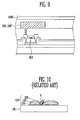
- FIG. 9 is an enlarged cross-sectional view of part A of FIG. 8.
- FIG. 10 is a detailed schematic cross-sectional diagram of a conventional light emitting unit for use in a conventional organic light emitting display.
- upper and lower electrodes of a light emitting unit for use in an organic light emitting display may be insulated from each other, even when an organic light emitting layer does not completely insulate these electrodes, in accordance with various configurations, thus reducing or preventing formation of a dark spot, improving image quality.
- OLED organic light emitting display
- an organic light emitting display may include a thin film transistor (TFT) 210 formed on a substrate 201, and a light emitting unit 220.
- the TFT 210 may include a semiconductor layer 211, a gate electrode 212, and source-drain electrodes 213.
- the light emitting unit 220 may include a lower electrode 221 on the substrate electrically connected to the TFT 210, an organic light emitting layer 222 on the lower electrode, an upper electrode 223 on the organic light emitting layer, and a buffer layer, e.g., a polyol-based buffer layer 224, on the upper electrode 223.
- the polyol-based buffer layer 224 may render a predetermined thickness of the upper electrode to be non-conductive, i.e., may modify the predetermined thickness of the upper electrode to be a non-conductive material, e.g., to be an oxide.
- the polyol-based buffer layer 224 may extend over an entire OLED structure, i.e., may be continuous.
- a light emitting unit 220' may include a polyol-based buffer layer 224' that may only extend within a contact hole for each light emitting unit , i.e., may be discontinuous. All of the other elements of the OLED may be the same as those in FIG. 1, so discussion thereof will not be repeated.
- an OLED according to third and fourth embodiments of the present invention may further include a capping layer 225 on the polyol-based buffer layer 224, 224' of FIGS. 2 and 3, respectively. All of the other elements of the OLED may be the same as those in FIGS. 2 and 3, so discussion thereof will not be repeated.
- an OLED according to fifth and sixth embodiments of the present invention may further include a passivation layer 226 on the polyol-based buffer layer 224, 224' of FIGS. 2 and 3, respectively. All of the other elements of the OLED may be the same as those in FIGS. 1 and 2, respectively, so discussion thereof will not be repeated.
- the thin film transistor 210 formed on the substrate 201 may be formed by a method that is common in the art to have a structure that is common in the art.
- a buffer layer 202 may be selectively formed on the substrate 201.
- a semiconductor layer 211, including source-drain regions, may be formed on the buffer layer.
- source-drain electrodes 213 connected to the source-drain regions through contact holes may be formed on the interlayer insulating layer to form the thin film transistor 210.
- a light emitting unit 220 electrically connected to the thin film transistor 210 may be formed on the substrate where the thin film transistor 210 is formed.
- a lower electrode 221 may be electrically connected to one of the source-drain electrodes 213 of the thin film transistor 210 through a via hole formed on the passivation layer formed on the substrate 200.
- a conventional substrate for an OLED e.g., a glass substrate or a transparent plastic substrate having excellent transparency, surface flatness, and is easily dealt with and waterproof, may be used as the substrate 201.
- the lower electrode 221 formed on the substrate may be an anode electrode or a cathode electrode, and may be a reflective electrode or a transmissive electrode in accordance with front surface emission or rear surface emission operation of the OLED.
- the lower electrode 211 may be an anode electrode.
- the lower electrode 221 may be formed of a conductive material, e.g., a metal or an oxide, that has a high work function and into which holes may be easily injected, e.g., indium tin oxide (ITO), indium zinc oxide (IZO), Ni, Pt, Au, and Ir.
- ITO indium tin oxide
- IZO indium zinc oxide
- Ni Pt, Au
- Ir Ir
- An organic light emitting layer 222 may be formed on the lower electrode 221.
- the organic light emitting layer 222 may include an emission layer and at least one organic layer in addition to the emission layer.
- the at least one organic layer may have at least one of a hole injecting layer, a hole transporting layer, a hole suppressing layer, an electron transporting layer, and an electron injecting layer. Any of the emission layer, the hole injecting layer, the hole transporting layer, the hole suppressing layer, the electron transporting layer, and the electron injecting layer may be formed with methods and materials commonly used in the art.
- the hole injecting layer may be formed of CuPc or Starburst type amine by deposition or spin coating, although not limited to the above.
- the hole transporting layer may be formed of materials having hole transporting properties, e.g., N'-diphenyl-N,N'-bis(3-methylphenyl) 1,1-biphenyl 4,4'-diamine (hereinafter, TPD) by deposition, spin coating, etc.
- TPD N'-diphenyl-N,N'-bis(3-methylphenyl) 1,1-biphenyl 4,4'-diamine
- the emission layer may be formed of light emitting materials, e.g., aluminum tris(8-hydroxyquinoline) (Alq3), by deposition, spin coating, etc.
- the electron transporting layer may be formed of oxadiazole-based derivative by deposition, spin coating, etc.
- the upper electrode 223 may be formed on the organic light emitting layer 222.
- the upper electrode 223 may be an anode electrode or a cathode electrode.
- the cathode electrode may be formed of metals, e.g., Li, Mg, Al, Al-Li, Ca, Mg-In, Mg-Ag, etc. Therefore, the structure of the light emitting unit 220, 220' may vary from the lower electrode/the organic light emitting layer/the upper layer to the lower electrode/the hole injecting layer/the hole transporting layer/the organic light emitting layer/the hole suppressing layer/the electron transporting layer/the electron injecting layer/the upper electrode.
- a polyol-based buffer layer 224 may be formed on the upper electrode 223 by a method such as deposition, spin coating, etc., under the conditions similar to those used for forming the above layers. As illustrated in FIG. 8, in order to prevent the upper electrode 223 from being shorted due to a connection between the upper electrode 223 and the lower electrode 221 that may arise when the organic light emitting layer 222 is not uniformly deposited, e.g., due to particles that may exist on the lower electrode 221, the polyol-based buffer layer 224 modifies a predetermined thickness of the upper electrode 223 to be non-conductive, so that the upper and lower electrodes are insulated from each other. In order to modify the predetermined thickness of the upper electrode to be non-conductive, the predetermined thickness of the upper electrode 223 may be modified, e.g., to be an oxide or a nitride.
- the predetermined thickness of the upper electrode 223 may be modified to be a non-conductive oxide by forming the polyol-based buffer layer 224 on the upper electrode 223. That is, the -OH group of polyol may oxidize the metal of the upper electrode 223. In this case, oxidation occurs during formation of the - OH group of the polyol-based buffer layer 224, 224'.
- the thickness of the polyol-based buffer layer 224, 224' may be about 10 ⁇ to 100 ⁇ . Due to the oxidation of the upper electrode by the buffer layer having this thickness, the predetermined thickness of the non-conductive oxide layer will be less than 100 ⁇ , e.g., between 10 ⁇ to 30 ⁇ .
- the polyol-based buffer layer 224, 224' may be formed on the upper electrode 223 or may surround the sides and the front surface of the upper electrode 223.
- the polyol of which the buffer layer may be a compound having two or more -OH groups including, e.g., a monosaccharide such as glucose, fructose, mannose, galactose, or ribose, a disaccharide such as sucrose, maltose, or lactose, ethylene glycol, propylene glycol, 1,3-propandiol, 1,3- butanediol, 1,4-butanediol, 1,5-pentanediol, 1,6-hexanediol, neopentyl glycol, diethylene glycol, dipropylene glycol, triethylene glycol, tetraethylene glycol, dibutylene glycol, 2-methyl-1,3-pentanediol, 2,2,4-trimethyl-1,3-pentanediol, 1,4-cyclohexanedimethaneol, etc.
- a monosaccharide such as
- At least one protective layer for protecting the organic light emitting layer 222 may be formed on the polyol-based buffer layer 224, 224'.
- the capping layer 225 or the passivation layer 226 may be used as the protective layer.
- the capping layer 225 and the passivation layer 226 may be formed, e.g., by deposition or spin coating, transparent materials that are commonly used in the art.
- a mobile display 1000 may include a picture unit 1100 for displaying a picture and a display main body including a plurality of operation button units 1200.
- the OLED having the light emitting unit 220, 220' and the transistor 210 according to any of the exemplary embodiments of the present invention may be provided in the picture unit 1100.
- the OLED according to the present-invention may be applied to various displays, e.g., a personal digital assistant (PDA), an electronic pager, a video camera, a workstation, a picture telephone etc., besides the mobile telephone 1000 illustrated in FIG. 9.
- PDA personal digital assistant
- the polyol-based buffer layer may be formed on the upper electrode so that the predetermined thickness of the upper electrode is rendered non-conductive.
- the organic light emitting layer is non-uniformly deposited, e.g., due to particles that may exist on the lower electrode, only the non-conductive surface of the upper electrode will contact the lower electrode. Therefore, it is possible to prevent the light emitting unit from being shorted, to prevent the dark point from being generated, and to improve picture quality.
Abstract
Description
- The present invention relates to an organic light emitting display, a method of fabricating the same, and a mobile display including the organic light emitting display. More particularly, the present invention relates to an organic light emitting display that is capable of preventing a dark point from being generated, a method of fabricating the same, and a mobile display including the organic light emitting display.
- A conventional organic light emitting display (OLED) may include a light emitting unit 120, as illustrated in FIG. 10, to be electrically connected to, e.g., a thin film transistor (TFT) (not shown) on a substrate 100. The light emitting unit 120 may include a
lower electrode 121, an organic light emitting layer 122, and anupper electrode 123. - In the conventional OLED having the above-described structure, as illustrated in FIG. 10, the organic light emitting layer 122 may not be uniformly deposited due, e.g., to particles that may exist on the
lower electrode 121. Therefore, theupper electrode 123 may be connected to thelower electrode 121 at a junction where the particles exist. Therefore, the light emitting unit 120 may short circuit, resulting in a dark spot. As a result, a light emitting region may be reduced, deteriorating picture quality. - The present invention is therefore directed to an organic light emitting display, a method of fabricating the same, and a mobile display including the organic light emitting display, which substantially overcome one or more of the problems due to the limitations and disadvantages of the related art.
- It is therefore an object of an embodiment of the present invention to insulate the upper and lower electrodes from each other to prevent a dark spot from being generated.
- Embodiments of the invention therefore set out to provide a buffer layer on the upper electrode that can render a predetermined thickness of the upper electrode non-conductive.
- Embodiments of the invention also set out to provide an organic light emitting display that is capable of reducing or preventing a dark spot from being generated.
- Embodiments of the invention also set out to provide a method of fabricating an organic light emitting display that is capable of reducing or preventing a dark spot from being generated.
- Embodiments of the invention also set out to provide a mobile display including the organic light emitting display that is capable of reducing or preventing a dark spot from being generated.
- At least one of the above and other features and advantages of the present invention maybe realized by providing an organic light emitting display, including a transistor on a substrate, a lower electrode on the substrate, the lower electrode being electrically connected to the transistor, an organic light emitting layer on the lower electrode, an upper electrode on the organic light emitting layer, and a buffer layer formed on the upper electrode to modify a predetermined thickness of the upper electrode to be non-conductive material.
- The buffer layer may be about 10Å to 100Å thick. The predetermined thickness of the upper electrode may be about 10Å to 30Å. The non-conductive material of the predetermined thickness may be an oxide.
- The buffer layer may be a polyol-based buffer layer. The polyol of which the polyol-based buffer layer may be formed may be a compound including at least two OH groups in one molecule.
- The upper electrode may have a smaller work function than the lower electrode.
- The organic light emitting display may include at least one protective layer on the buffer layer. The protective layer may be a passivation layer or a capping layer.
- The organic light emitting layer may include at least one organic layer having at least one of a hole injecting layer, a hole transporting layer, an electron transporting layer, and an electron injecting layer.
- At least one of the above and other features and advantages may be realized by providing a method of fabricating an organic light emitting display, the method including forming a lower electrode electrically connected to a transistor on a substrate, forming an organic light emitting layer on the lower electrode, forming an upper electrode on the organic light emitting layer, and forming a buffer layer on the upper electrode in order to modify a predetermined thickness of the upper electrode to be a non-conductive material.
- At least one of the above and other features and advantages may be realized by providing a mobile display including a display main body having a picture unit for displaying a picture, the picture unit including an organic light emitting display having any of the above elements.
- Embodiments of the invention will now be described by way of example and with reference to the accompanying drawings, in which:-
- FIG. 1 is a cross-sectional view of an organic light emitting display according to a first embodiment of the present invention;
- FIG. 2 is a cross-sectional view of an organic light emitting display according to a second embodiment of the present invention;
- FIG. 3 is a cross-sectional view of an organic light emitting display according to a third embodiment of the present invention;
- FIG. 4 is a cross-sectional view of an organic light emitting display according to a fourth embodiment of the present invention;
- FIG. 5 is a cross-sectional view of an organic light emitting display according to a fifth embodiment of the present invention;
- FIG. 6 is a cross-sectional view of an organic light emitting display according to a sixth embodiment of the present invention;
- FIG. 7 is a detailed schematic cross-sectional diagram of a light emitting unit according to embodiments of the present invention;
- FIG. 8 is as schematic a mobile display including an organic light emitting display according to an embodiment of the present invention;
- FIG. 9 is an enlarged cross-sectional view of part A of FIG. 8; and
- FIG. 10 is a detailed schematic cross-sectional diagram of a conventional light emitting unit for use in a conventional organic light emitting display.
- The present invention will now be described more fully hereinafter with reference to the accompanying drawings, in which various embodiments of the invention are illustrated. The invention may, however, be embodied in different forms and should not be construed as limited to the embodiments set forth herein.
- In the figures, the dimensions of layers and regions may be exaggerated for clarity of illustration. It will also be understood that when a layer or element is referred to as being "on" another layer or substrate, it can be directly on the other layer or substrate, or intervening layers may also be present. Further, it will be understood that when a layer is referred to as being "under" another layer, it can be directly under, and one or more intervening layers may also be present. In addition, it will also be understood that when a layer is referred to as being "between" two layers, it can be the only layer between the two layers, or one or more intervening layers may also be present. Like reference numerals refer to like elements throughout.
- As discussed in detail below, upper and lower electrodes of a light emitting unit for use in an organic light emitting display (OLED) may be insulated from each other, even when an organic light emitting layer does not completely insulate these electrodes, in accordance with various configurations, thus reducing or preventing formation of a dark spot, improving image quality. By converting a predetermined thickness of an upper electrode into a non-conductive material, any inadvertent contact between the upper and lower electrodes due to discontinuities in the organic light emitting layer may not resort in shorting the light emitting unit.
- Referring to FIG. 1, an organic light emitting display (OLED) according to an embodiment of the present invention may include a thin film transistor (TFT) 210 formed on a
substrate 201, and alight emitting unit 220. The TFT 210 may include asemiconductor layer 211, agate electrode 212, and source-drain electrodes 213. Thelight emitting unit 220 may include alower electrode 221 on the substrate electrically connected to theTFT 210, an organiclight emitting layer 222 on the lower electrode, anupper electrode 223 on the organic light emitting layer, and a buffer layer, e.g., a polyol-basedbuffer layer 224, on theupper electrode 223. The polyol-basedbuffer layer 224 may render a predetermined thickness of the upper electrode to be non-conductive, i.e., may modify the predetermined thickness of the upper electrode to be a non-conductive material, e.g., to be an oxide. - In a first embodiment of the present invention, as illustrated in FIG. 1, the polyol-based
buffer layer 224 may extend over an entire OLED structure, i.e., may be continuous. Alternatively, an OLED according to a second embodiment of the present invention, as illustrated in FIG. 2, a light emitting unit 220' may include a polyol-based buffer layer 224' that may only extend within a contact hole for each light emitting unit , i.e., may be discontinuous. All of the other elements of the OLED may be the same as those in FIG. 1, so discussion thereof will not be repeated. - Referring to FIGS. 3 and 4, an OLED according to third and fourth embodiments of the present invention may further include a
capping layer 225 on the polyol-basedbuffer layer 224, 224' of FIGS. 2 and 3, respectively. All of the other elements of the OLED may be the same as those in FIGS. 2 and 3, so discussion thereof will not be repeated. - Referring to FIGS. 5 and 6, an OLED according to fifth and sixth embodiments of the present invention may further include a
passivation layer 226 on the polyol-basedbuffer layer 224, 224' of FIGS. 2 and 3, respectively. All of the other elements of the OLED may be the same as those in FIGS. 1 and 2, respectively, so discussion thereof will not be repeated. - The
thin film transistor 210 formed on thesubstrate 201 may be formed by a method that is common in the art to have a structure that is common in the art. For example, abuffer layer 202 may be selectively formed on thesubstrate 201. Then, asemiconductor layer 211, including source-drain regions, may be formed on the buffer layer. After forming a gate insulating layer on the substrate including thesemiconductor layer 211 and forming agate electrode 212 on the gate insulating layer, source-drain electrodes 213 connected to the source-drain regions through contact holes may be formed on the interlayer insulating layer to form thethin film transistor 210. - A
light emitting unit 220 electrically connected to thethin film transistor 210 may be formed on the substrate where thethin film transistor 210 is formed. To be specific, alower electrode 221 may be electrically connected to one of the source-drain electrodes 213 of thethin film transistor 210 through a via hole formed on the passivation layer formed on the substrate 200. - A conventional substrate for an OLED, e.g., a glass substrate or a transparent plastic substrate having excellent transparency, surface flatness, and is easily dealt with and waterproof, may be used as the
substrate 201. - The
lower electrode 221 formed on the substrate may be an anode electrode or a cathode electrode, and may be a reflective electrode or a transmissive electrode in accordance with front surface emission or rear surface emission operation of the OLED. - The
lower electrode 211 may be an anode electrode. When thelower electrode 221 is the anode electrode, thelower electrode 221 may be formed of a conductive material, e.g., a metal or an oxide, that has a high work function and into which holes may be easily injected, e.g., indium tin oxide (ITO), indium zinc oxide (IZO), Ni, Pt, Au, and Ir. - An organic
light emitting layer 222 may be formed on thelower electrode 221. The organiclight emitting layer 222 may include an emission layer and at least one organic layer in addition to the emission layer. The at least one organic layer may have at least one of a hole injecting layer, a hole transporting layer, a hole suppressing layer, an electron transporting layer, and an electron injecting layer. Any of the emission layer, the hole injecting layer, the hole transporting layer, the hole suppressing layer, the electron transporting layer, and the electron injecting layer may be formed with methods and materials commonly used in the art. - For example, the hole injecting layer may be formed of CuPc or Starburst type amine by deposition or spin coating, although not limited to the above. The hole transporting layer may be formed of materials having hole transporting properties, e.g., N'-diphenyl-N,N'-bis(3-methylphenyl) 1,1-biphenyl 4,4'-diamine (hereinafter, TPD) by deposition, spin coating, etc. The emission layer may be formed of light emitting materials, e.g., aluminum tris(8-hydroxyquinoline) (Alq3), by deposition, spin coating, etc. The electron transporting layer may be formed of oxadiazole-based derivative by deposition, spin coating, etc.
- The
upper electrode 223 may be formed on the organiclight emitting layer 222. Theupper electrode 223 may be an anode electrode or a cathode electrode. When theupper electrode 223 is the cathode electrode, the cathode electrode may be formed of metals, e.g., Li, Mg, Al, Al-Li, Ca, Mg-In, Mg-Ag, etc. Therefore, the structure of thelight emitting unit 220, 220' may vary from the lower electrode/the organic light emitting layer/the upper layer to the lower electrode/the hole injecting layer/the hole transporting layer/the organic light emitting layer/the hole suppressing layer/the electron transporting layer/the electron injecting layer/the upper electrode. - A polyol-based
buffer layer 224 may be formed on theupper electrode 223 by a method such as deposition, spin coating, etc., under the conditions similar to those used for forming the above layers. As illustrated in FIG. 8, in order to prevent theupper electrode 223 from being shorted due to a connection between theupper electrode 223 and thelower electrode 221 that may arise when the organiclight emitting layer 222 is not uniformly deposited, e.g., due to particles that may exist on thelower electrode 221, the polyol-basedbuffer layer 224 modifies a predetermined thickness of theupper electrode 223 to be non-conductive, so that the upper and lower electrodes are insulated from each other. In order to modify the predetermined thickness of the upper electrode to be non-conductive, the predetermined thickness of theupper electrode 223 may be modified, e.g., to be an oxide or a nitride. - The predetermined thickness of the
upper electrode 223 may be modified to be a non-conductive oxide by forming the polyol-basedbuffer layer 224 on theupper electrode 223. That is, the -OH group of polyol may oxidize the metal of theupper electrode 223. In this case, oxidation occurs during formation of the - OH group of the polyol-basedbuffer layer 224, 224'. - The thickness of the polyol-based
buffer layer 224, 224' may be about 10Å to 100Å. Due to the oxidation of the upper electrode by the buffer layer having this thickness, the predetermined thickness of the non-conductive oxide layer will be less than 100Å, e.g., between 10Å to 30Å. The polyol-basedbuffer layer 224, 224' may be formed on theupper electrode 223 or may surround the sides and the front surface of theupper electrode 223. - The polyol of which the buffer layer may be a compound having two or more -OH groups including, e.g., a monosaccharide such as glucose, fructose, mannose, galactose, or ribose, a disaccharide such as sucrose, maltose, or lactose, ethylene glycol, propylene glycol, 1,3-propandiol, 1,3- butanediol, 1,4-butanediol, 1,5-pentanediol, 1,6-hexanediol, neopentyl glycol, diethylene glycol, dipropylene glycol, triethylene glycol, tetraethylene glycol, dibutylene glycol, 2-methyl-1,3-pentanediol, 2,2,4-trimethyl-1,3-pentanediol, 1,4-cyclohexanedimethaneol, etc.
- At least one protective layer for protecting the organic
light emitting layer 222 may be formed on the polyol-basedbuffer layer 224, 224'. Thecapping layer 225 or thepassivation layer 226 may be used as the protective layer. Thecapping layer 225 and thepassivation layer 226 may be formed, e.g., by deposition or spin coating, transparent materials that are commonly used in the art. - Referring to FIGS. 8 and 9, a
mobile display 1000 may include apicture unit 1100 for displaying a picture and a display main body including a plurality ofoperation button units 1200. As illustrated in the cross-sectional detail of FIG. 9, the OLED having thelight emitting unit 220, 220' and thetransistor 210 according to any of the exemplary embodiments of the present invention may be provided in thepicture unit 1100. - The OLED according to the present-invention may be applied to various displays, e.g., a personal digital assistant (PDA), an electronic pager, a video camera, a workstation, a picture telephone etc., besides the
mobile telephone 1000 illustrated in FIG. 9. - As described above, according to the present invention, the polyol-based buffer layer may be formed on the upper electrode so that the predetermined thickness of the upper electrode is rendered non-conductive. Thus, even if the organic light emitting layer is non-uniformly deposited, e.g., due to particles that may exist on the lower electrode, only the non-conductive surface of the upper electrode will contact the lower electrode. Therefore, it is possible to prevent the light emitting unit from being shorted, to prevent the dark point from being generated, and to improve picture quality.
- Embodiments of the present invention have been disclosed herein, and although specific terms are employed, they are used and are to be interpreted in a generic and descriptive sense only and not for purpose of limitation. Accordingly, it will be understood by those of ordinary skill in the art that various changes in form and details may be made without departing from the scope of the present invention as set forth in the following claims.
Claims (12)
- An organic light emitting display, comprising:a transistor on a substrate;a lower electrode on the substrate, the lower electrode being electrically connected to the transistor;an organic light emitting layer on the lower electrode;an upper electrode on the organic light emitting layer; anda buffer layer formed on the upper electrode to modify a predetermined thickness of the upper electrode to be a non-conductive material.
- An organic light emitting display as claimed in claim 1, wherein a thickness of the buffer layer is about 10Å to 100Å.
- An organic light emitting display as claimed in claim 1 or 2, wherein the predetermined thickness of the upper electrode is about 10Å to 30Å.
- An organic light emitting display as claimed in claim 1, 2 or 3 wherein the buffer layer is a polyol-based buffer layer.
- An organic light emitting display as claimed in claim 4, wherein polyol of which the polyol-based buffer layer is formed of a compound including at least two -OH groups.
- An organic light emitting display as claimed in any preceding claim, wherein the upper electrode is a cathode.
- An organic light emitting display as claimed in any preceding claim, further comprising at least one protective layer on the buffer layer.
- An organic light emitting display as claimed in claim 7, wherein the protective layer is a passivation layer or a capping layer.
- An organic light emitting display as claimed in any preceding claim, wherein the organic light emitting layer further comprises at least one organic layer including at least one of a hole injecting layer, a hole transporting layer, an electron transporting layer, and an electron injecting layer.
- An organic light emitting display as claimed in any preceding claim, wherein the non-conductive material is an oxide.
- A method of fabricating an organic light emitting display, the method comprising:forming a lower electrode electrically connected to a transistor on a substrate;forming an organic light emitting layer on the lower electrode;forming an upper electrode on the organic light emitting layer; andforming a buffer layer on the upper electrode in order to modify a predetermined thickness of the upper electrode to be a non-conductive material.
- A mobile display including a display main body having a picture unit for displaying a picture, the picture unit including an organic light emitting display as set out in one of claims 1 to 10.
Applications Claiming Priority (1)
| Application Number | Priority Date | Filing Date | Title |
|---|---|---|---|
| KR1020050099381A KR100707602B1 (en) | 2005-10-20 | 2005-10-20 | Organic emitting device and method for preparing the same |
Publications (3)
| Publication Number | Publication Date |
|---|---|
| EP1777759A2 true EP1777759A2 (en) | 2007-04-25 |
| EP1777759A3 EP1777759A3 (en) | 2010-08-11 |
| EP1777759B1 EP1777759B1 (en) | 2017-08-09 |
Family
ID=37591687
Family Applications (1)
| Application Number | Title | Priority Date | Filing Date |
|---|---|---|---|
| EP06255407.6A Expired - Fee Related EP1777759B1 (en) | 2005-10-20 | 2006-10-20 | Organic light emitting display, method of fabricating the same, and mobile display including the organic light emitting display |
Country Status (6)
| Country | Link |
|---|---|
| US (1) | US7863601B2 (en) |
| EP (1) | EP1777759B1 (en) |
| JP (1) | JP4422129B2 (en) |
| KR (1) | KR100707602B1 (en) |
| CN (1) | CN1953200A (en) |
| TW (1) | TWI327783B (en) |
Families Citing this family (6)
| Publication number | Priority date | Publication date | Assignee | Title |
|---|---|---|---|---|
| KR100918403B1 (en) * | 2008-02-12 | 2009-09-24 | 삼성모바일디스플레이주식회사 | Organic light emitting display apparatus and method for manufacturing the same |
| JP2012155953A (en) * | 2011-01-25 | 2012-08-16 | Sony Corp | Organic el display device and electronic apparatus |
| TWI602901B (en) * | 2012-12-11 | 2017-10-21 | 半導體能源研究所股份有限公司 | Light-emitting element, light-emitting device, electronic device, and lighting device |
| KR20140088369A (en) * | 2013-01-02 | 2014-07-10 | 삼성디스플레이 주식회사 | Organic light emitting diode display |
| WO2015093100A1 (en) * | 2013-12-19 | 2015-06-25 | シャープ株式会社 | Display device and method for driving same |
| KR102478677B1 (en) * | 2017-12-29 | 2022-12-16 | 엘지디스플레이 주식회사 | Organic Light Emitting Device and Organic Light Emitting Display Device |
Family Cites Families (20)
| Publication number | Priority date | Publication date | Assignee | Title |
|---|---|---|---|---|
| JP2844964B2 (en) | 1991-06-11 | 1999-01-13 | 松下電器産業株式会社 | Manufacturing method of EL display device |
| DE4225835A1 (en) | 1992-08-05 | 1994-02-10 | Merck Patent Gmbh | Process for the preparation of imidazopyridines |
| JP3615817B2 (en) | 1995-02-14 | 2005-02-02 | 株式会社アルバック | Method for manufacturing organic electroluminescence element |
| JPH09274990A (en) | 1996-04-08 | 1997-10-21 | Mitsubishi Chem Corp | Organic electroluminescence element, and its manufacture |
| DE19943149A1 (en) * | 1999-09-09 | 2001-04-05 | Siemens Ag | Process for encapsulating components |
| JP3565263B2 (en) | 2000-05-17 | 2004-09-15 | 日本精機株式会社 | Manufacturing method of organic EL device |
| JP2002025769A (en) | 2000-07-12 | 2002-01-25 | Nippon Seiki Co Ltd | Organic el panel and its manufacturing method |
| US7041609B2 (en) | 2002-08-28 | 2006-05-09 | Micron Technology, Inc. | Systems and methods for forming metal oxides using alcohols |
| JP2004103442A (en) | 2002-09-11 | 2004-04-02 | Ulvac Japan Ltd | Organic electroluminescent element and method for manufacturing the same |
| JP3953404B2 (en) * | 2002-10-21 | 2007-08-08 | インターナショナル・ビジネス・マシーンズ・コーポレーション | ORGANIC ELECTROLUMINESCENCE ELEMENT, METHOD FOR PRODUCING THE ORGANIC ELECTROLUMINESCENCE ELEMENT, AND ORGANIC ELECTROLUMINESCENCE DISPLAY DEVICE |
| TWI232693B (en) | 2002-10-24 | 2005-05-11 | Toppoly Optoelectronics Corp | Hygroscopic passivation structure of an organic electroluminescent display |
| JP4138672B2 (en) * | 2003-03-27 | 2008-08-27 | セイコーエプソン株式会社 | Manufacturing method of electro-optical device |
| US20050008896A1 (en) * | 2003-07-11 | 2005-01-13 | Orient Chemical Ind., Ltd. | Luminous organic compound and manufacturing method |
| TWI310977B (en) | 2003-09-19 | 2009-06-11 | Innolux Display Corp | A packaging structure of an oled and a method of manufacturing the same thereof |
| JP4479381B2 (en) | 2003-09-24 | 2010-06-09 | セイコーエプソン株式会社 | Electro-optical device, method of manufacturing electro-optical device, and electronic apparatus |
| WO2005034583A1 (en) | 2003-10-03 | 2005-04-14 | Jsr Corporation | Transparent sealing material for organic el device |
| JP4475084B2 (en) | 2003-10-03 | 2010-06-09 | Jsr株式会社 | Transparent sealing material for organic EL elements |
| WO2005076756A2 (en) | 2004-02-12 | 2005-08-25 | Samsung Electronics Co., Ltd. | Flat panel display apparatus |
| US7371143B2 (en) | 2004-10-20 | 2008-05-13 | Corning Incorporated | Optimization of parameters for sealing organic emitting light diode (OLED) displays |
| TWI319893B (en) | 2006-08-31 | 2010-01-21 | Nitride semiconductor substrate, method for forming a nitride semiconductor layer and method for separating the nitride semiconductor layer from the substrate |
-
2005
- 2005-10-20 KR KR1020050099381A patent/KR100707602B1/en not_active IP Right Cessation
-
2006
- 2006-08-16 JP JP2006222077A patent/JP4422129B2/en not_active Expired - Fee Related
- 2006-10-18 TW TW095138359A patent/TWI327783B/en not_active IP Right Cessation
- 2006-10-19 US US11/583,060 patent/US7863601B2/en not_active Expired - Fee Related
- 2006-10-20 CN CNA2006101402375A patent/CN1953200A/en active Pending
- 2006-10-20 EP EP06255407.6A patent/EP1777759B1/en not_active Expired - Fee Related
Non-Patent Citations (1)
| Title |
|---|
| None |
Also Published As
| Publication number | Publication date |
|---|---|
| US20070090340A1 (en) | 2007-04-26 |
| US7863601B2 (en) | 2011-01-04 |
| EP1777759A3 (en) | 2010-08-11 |
| CN1953200A (en) | 2007-04-25 |
| TW200719501A (en) | 2007-05-16 |
| KR100707602B1 (en) | 2007-04-13 |
| EP1777759B1 (en) | 2017-08-09 |
| TWI327783B (en) | 2010-07-21 |
| JP4422129B2 (en) | 2010-02-24 |
| JP2007115662A (en) | 2007-05-10 |
Similar Documents
| Publication | Publication Date | Title |
|---|---|---|
| US9711575B2 (en) | Organic light emitting display device and method of manufacturing an organic light emitting display device | |
| US6902943B2 (en) | Flat panel display device with anti-reflection layer having concentration gradient and fabrication method thereof | |
| CN1246824C (en) | Display device | |
| CN110391348A (en) | A kind of display panel and display device | |
| KR100879294B1 (en) | Organic light emitting display | |
| US8344620B2 (en) | Active matrix electroluminescence device having a metallic protective layer and method for fabricating the same | |
| EP1783835A2 (en) | Flat panel display apparatus | |
| US7863601B2 (en) | Organic light emitting display, method of fabricating the same, and mobile display including the organic light emitting display | |
| KR100932935B1 (en) | Organic light emitting device and organic light emitting display device including the same | |
| US9966568B2 (en) | Organic light emitting display apparatus having cover unit with different thickness | |
| US20130288414A1 (en) | Organic light-emitting display apparatus and method of manufacturing the same | |
| KR20180049844A (en) | Etching composition and manufacturing method of wire patter and organic light emitting display device using the same | |
| KR101022650B1 (en) | Flat panel display apparatus | |
| KR100749420B1 (en) | Organic light emitting display | |
| US20140353627A1 (en) | Display device and method of manufacturing the same | |
| KR100708863B1 (en) | Organic light emitting display | |
| CN111312826B (en) | Display panel, manufacturing method thereof, display module and electronic device | |
| US20220328580A1 (en) | Display device |
Legal Events
| Date | Code | Title | Description |
|---|---|---|---|
| PUAI | Public reference made under article 153(3) epc to a published international application that has entered the european phase |
Free format text: ORIGINAL CODE: 0009012 |
|
| 17P | Request for examination filed |
Effective date: 20061026 |
|
| AK | Designated contracting states |
Kind code of ref document: A2 Designated state(s): AT BE BG CH CY CZ DE DK EE ES FI FR GB GR HU IE IS IT LI LT LU LV MC NL PL PT RO SE SI SK TR |
|
| AX | Request for extension of the european patent |
Extension state: AL BA HR MK YU |
|
| RAP1 | Party data changed (applicant data changed or rights of an application transferred) |
Owner name: SAMSUNG MOBILE DISPLAY CO., LTD. |
|
| PUAL | Search report despatched |
Free format text: ORIGINAL CODE: 0009013 |
|
| AK | Designated contracting states |
Kind code of ref document: A3 Designated state(s): AT BE BG CH CY CZ DE DK EE ES FI FR GB GR HU IE IS IT LI LT LU LV MC NL PL PT RO SE SI SK TR |
|
| AX | Request for extension of the european patent |
Extension state: AL BA HR MK RS |
|
| AKX | Designation fees paid |
Designated state(s): DE FR GB |
|
| RAP1 | Party data changed (applicant data changed or rights of an application transferred) |
Owner name: SAMSUNG DISPLAY CO., LTD. |
|
| 17Q | First examination report despatched |
Effective date: 20140307 |
|
| RAP1 | Party data changed (applicant data changed or rights of an application transferred) |
Owner name: SAMSUNG DISPLAY CO., LTD. |
|
| GRAP | Despatch of communication of intention to grant a patent |
Free format text: ORIGINAL CODE: EPIDOSNIGR1 |
|
| RIC1 | Information provided on ipc code assigned before grant |
Ipc: H01L 51/52 20060101AFI20170119BHEP Ipc: H01L 27/32 20060101ALI20170119BHEP |
|
| INTG | Intention to grant announced |
Effective date: 20170203 |
|
| GRAS | Grant fee paid |
Free format text: ORIGINAL CODE: EPIDOSNIGR3 |
|
| GRAJ | Information related to disapproval of communication of intention to grant by the applicant or resumption of examination proceedings by the epo deleted |
Free format text: ORIGINAL CODE: EPIDOSDIGR1 |
|
| GRAL | Information related to payment of fee for publishing/printing deleted |
Free format text: ORIGINAL CODE: EPIDOSDIGR3 |
|
| GRAR | Information related to intention to grant a patent recorded |
Free format text: ORIGINAL CODE: EPIDOSNIGR71 |
|
| GRAA | (expected) grant |
Free format text: ORIGINAL CODE: 0009210 |
|
| INTC | Intention to grant announced (deleted) | ||
| AK | Designated contracting states |
Kind code of ref document: B1 Designated state(s): DE FR GB |
|
| INTG | Intention to grant announced |
Effective date: 20170703 |
|
| REG | Reference to a national code |
Ref country code: GB Ref legal event code: FG4D |
|
| REG | Reference to a national code |
Ref country code: DE Ref legal event code: R096 Ref document number: 602006053255 Country of ref document: DE |
|
| REG | Reference to a national code |
Ref country code: DE Ref legal event code: R119 Ref document number: 602006053255 Country of ref document: DE |
|
| PLBE | No opposition filed within time limit |
Free format text: ORIGINAL CODE: 0009261 |
|
| STAA | Information on the status of an ep patent application or granted ep patent |
Free format text: STATUS: NO OPPOSITION FILED WITHIN TIME LIMIT |
|
| 26N | No opposition filed |
Effective date: 20180511 |
|
| GBPC | Gb: european patent ceased through non-payment of renewal fee |
Effective date: 20171109 |
|
| REG | Reference to a national code |
Ref country code: FR Ref legal event code: ST Effective date: 20180629 |
|
| PG25 | Lapsed in a contracting state [announced via postgrant information from national office to epo] |
Ref country code: DE Free format text: LAPSE BECAUSE OF NON-PAYMENT OF DUE FEES Effective date: 20180501 |
|
| PG25 | Lapsed in a contracting state [announced via postgrant information from national office to epo] |
Ref country code: FR Free format text: LAPSE BECAUSE OF NON-PAYMENT OF DUE FEES Effective date: 20171031 |
|
| PG25 | Lapsed in a contracting state [announced via postgrant information from national office to epo] |
Ref country code: GB Free format text: LAPSE BECAUSE OF NON-PAYMENT OF DUE FEES Effective date: 20171109 |