EP1777743A2 - Lead frame - Google Patents
Lead frame Download PDFInfo
- Publication number
- EP1777743A2 EP1777743A2 EP06122491A EP06122491A EP1777743A2 EP 1777743 A2 EP1777743 A2 EP 1777743A2 EP 06122491 A EP06122491 A EP 06122491A EP 06122491 A EP06122491 A EP 06122491A EP 1777743 A2 EP1777743 A2 EP 1777743A2
- Authority
- EP
- European Patent Office
- Prior art keywords
- plating
- layer
- lead frame
- less
- thickness
- Prior art date
- Legal status (The legal status is an assumption and is not a legal conclusion. Google has not performed a legal analysis and makes no representation as to the accuracy of the status listed.)
- Ceased
Links
Images



Classifications
-
- H—ELECTRICITY
- H10—SEMICONDUCTOR DEVICES; ELECTRIC SOLID-STATE DEVICES NOT OTHERWISE PROVIDED FOR
- H10W—GENERIC PACKAGES, INTERCONNECTIONS, CONNECTORS OR OTHER CONSTRUCTIONAL DETAILS OF DEVICES COVERED BY CLASS H10
- H10W70/00—Package substrates; Interposers; Redistribution layers [RDL]
- H10W70/40—Leadframes
- H10W70/456—Materials
- H10W70/457—Materials of metallic layers on leadframes
-
- H—ELECTRICITY
- H05—ELECTRIC TECHNIQUES NOT OTHERWISE PROVIDED FOR
- H05K—PRINTED CIRCUITS; CASINGS OR CONSTRUCTIONAL DETAILS OF ELECTRIC APPARATUS; MANUFACTURE OF ASSEMBLAGES OF ELECTRICAL COMPONENTS
- H05K3/00—Apparatus or processes for manufacturing printed circuits
- H05K3/30—Assembling printed circuits with electric components, e.g. with resistors
- H05K3/32—Assembling printed circuits with electric components, e.g. with resistors electrically connecting electric components or wires to printed circuits
- H05K3/34—Assembling printed circuits with electric components, e.g. with resistors electrically connecting electric components or wires to printed circuits by soldering
- H05K3/341—Surface mounted components
- H05K3/3421—Leaded components
- H05K3/3426—Leaded components characterised by the leads
-
- H—ELECTRICITY
- H10—SEMICONDUCTOR DEVICES; ELECTRIC SOLID-STATE DEVICES NOT OTHERWISE PROVIDED FOR
- H10W—GENERIC PACKAGES, INTERCONNECTIONS, CONNECTORS OR OTHER CONSTRUCTIONAL DETAILS OF DEVICES COVERED BY CLASS H10
- H10W72/00—Interconnections or connectors in packages
- H10W72/071—Connecting or disconnecting
- H10W72/075—Connecting or disconnecting of bond wires
-
- H—ELECTRICITY
- H10—SEMICONDUCTOR DEVICES; ELECTRIC SOLID-STATE DEVICES NOT OTHERWISE PROVIDED FOR
- H10W—GENERIC PACKAGES, INTERCONNECTIONS, CONNECTORS OR OTHER CONSTRUCTIONAL DETAILS OF DEVICES COVERED BY CLASS H10
- H10W72/00—Interconnections or connectors in packages
- H10W72/50—Bond wires
- H10W72/551—Materials of bond wires
- H10W72/552—Materials of bond wires comprising metals or metalloids, e.g. silver
-
- H—ELECTRICITY
- H10—SEMICONDUCTOR DEVICES; ELECTRIC SOLID-STATE DEVICES NOT OTHERWISE PROVIDED FOR
- H10W—GENERIC PACKAGES, INTERCONNECTIONS, CONNECTORS OR OTHER CONSTRUCTIONAL DETAILS OF DEVICES COVERED BY CLASS H10
- H10W72/00—Interconnections or connectors in packages
- H10W72/90—Bond pads, in general
- H10W72/951—Materials of bond pads
- H10W72/952—Materials of bond pads comprising metals or metalloids, e.g. PbSn, Ag or Cu
-
- H—ELECTRICITY
- H10—SEMICONDUCTOR DEVICES; ELECTRIC SOLID-STATE DEVICES NOT OTHERWISE PROVIDED FOR
- H10W—GENERIC PACKAGES, INTERCONNECTIONS, CONNECTORS OR OTHER CONSTRUCTIONAL DETAILS OF DEVICES COVERED BY CLASS H10
- H10W74/00—Encapsulations, e.g. protective coatings
-
- H—ELECTRICITY
- H10—SEMICONDUCTOR DEVICES; ELECTRIC SOLID-STATE DEVICES NOT OTHERWISE PROVIDED FOR
- H10W—GENERIC PACKAGES, INTERCONNECTIONS, CONNECTORS OR OTHER CONSTRUCTIONAL DETAILS OF DEVICES COVERED BY CLASS H10
- H10W90/00—Package configurations
- H10W90/701—Package configurations characterised by the relative positions of pads or connectors relative to package parts
- H10W90/751—Package configurations characterised by the relative positions of pads or connectors relative to package parts of bond wires
- H10W90/756—Package configurations characterised by the relative positions of pads or connectors relative to package parts of bond wires between a chip and a stacked lead frame, conducting package substrate or heat sink
Definitions
- the present invention relates to a lead frame, in particular to a plated lead frame for use in semiconductor devices.
- Printed circuit boards for implementing the semiconductor devices are also required to be thin, small and multilayered.
- the semiconductor device is implemented on the printed circuit board by reflowing.
- FIGS. 9A, 9B and 9C show how a semiconductor device is implemented on a board.
- a semiconductor device 32 is prepared by mounting a semiconductor element on a lead frame and sealing it into a package with a mold resin 33.
- solder paste 31 is applied onto electrode pads (not shown) provided on a printed circuit board (wiring board) 30. Then, in a mounting step shown in FIG. 9B, the semiconductor device 32 is mounted on the printed circuit board 30. Then, in a reflowing step shown in FIG. 9C, the whole device including the printed circuit board 30 and the semiconductor device 32 is heated at a high temperature to melt the solder paste 31. The solder paste 31 is then cooled, thereby fixing and connecting the semiconductor device 32 to the print circuit board 30.
- outer leads 34 electrically conducted with electrode pads in the semiconductor element are electrically connected to the printed circuit board 30 via the solder paste 31.
- the bottommost surface of each of the outer leads 34 of the semiconductor device 32 is generally called a mounting surface 35.
- the outer leads 34 are configured such that coplanarity 36 indicating flatness of the mounting surface 35 as shown in FIG. 10 is in the range of several tens of ⁇ m.
- the semiconductor device and the printed circuit board are deformed by various loads applied thereto while the temperature rises from a normal temperature of about 25°C to a high temperature of about 250°C.
- the semiconductor device 32 is deformed due to the difference in thermal expansion coefficient between the outer leads 34 principally made of iron or copper and the mold resin 33. If the coplanarity 36 is high, the outer leads 34 are deformed to be lifted above the printed circuit board 30.
- the printed circuit board 30 which is made thin or multilayered is also deformed under the high temperature during the reflowing step.
- the deformation of these components synergistically causes defects, even if the mounting surfaces 35 of the outer leads 34 are in contact with the solder paste 31.
- the solder paste 31 does not achieve good wicking, i.e., solder fillet is not formed, or alternatively, the outer leads 34 are lifted above the solder paste 31 to fail to establish electrical connection, thereby leading to solder joint open failure.
- the surface of the lead frame is plated to improve wettability between the outer leads 34 and the solder paste 31.
- solder paste 31 In recent years, from the aspect of environment issues, lead free solder paste, such as SnAgCu, SnZn and SnAgBiIn, are used as the solder paste 31 in many cases.
- the lead free solder pastes are poorer in wettability than conventional Sn-37%Pb eutectic solder and are likely to cause the defects such as the failure in solder fillet formation and the solder joint open failure. Therefore, a plating having good wettability with the lead free solder paste is required.
- the plating itself is molten under the high temperature condition during the reflowing step. Therefore, even if the lead free solder paste is used, the defect derived from the solder paste's lack of good wicking characteristics is less likely to occur.
- the Pb-containing plating will be restricted only in some very limited locations in electronic products. Thus, the plating of this kind is not available for general use.
- a lead free plating e.g., a SnBi plating (a two-layer plating including a tin layer and a 2% Bi layer formed thereon)
- the SnBi plating itself is molten due to its low melting point just like the SnPb eutectic plating. Therefore, the problem of the solder paste's lack of good wicking characteristics does not occur.
- the palladium-based metallic plating which has been adopted as a lead free plating by many manufacturers is used (e.g., a three-layer plating of nickel 20 /palladium 24 /gold 28 as shown in FIG. 11 ).
- the palladium-based metallic plating is not molten because its melting point is much higher than the high temperature condition during the reflowing step.
- the failure in solder fillet formation and the solder joint open failure have been less likely to occur even if the lead free solder paste is used. It is because the outer leads have been arranged at a pitch of 0.6 mm or more (e.g., see Japanese Unexamined Patent Publication H4-115558 ).
- the semiconductor device and the wiring board have been fabricated under finer design rules. Accordingly, the area of connector lands has been reduced and the area of openings in a metal mask used for solder printing has also been reduced. As a result, the solder paste does not easily come off the openings of the printing mask, thereby causing lack of the solder paste on the wiring board. Even if the printing succeeds, the total amount of the solder printed on the minuscule regions is smaller than it used to be. With the trend toward the smaller pitch, in particular when the pitch of the outer leads is reduced to less than 0.6 mm, the plated outer leads as disclosed by Japanese Unexamined Patent Publication H4-115558 bring about the failure in solder fillet formation or the solder joint open failure.
- the inner leads are plated by Ag spot plating. This brings about considerable increase in manufacturing cost.
- An object of the present invention is to provide a lead frame coated with a plating which ensures the wettability of the lead frame and the lead free solder even if the outer lead pitch is reduced.
- the lead frame of the present invention includes a die pad for mounting a semiconductor element thereon, inner leads electrically connected to electrode pads of the semiconductor element and outer leads connected to the inner leads to function as external terminals, wherein at least the ends of the outer leads opposite to the inner leads are coated with a four-layer plating, first three layers in the four-layer plating from the topmost surface thereof are made of Au, Ag and Pd, respectively, and the Ag layer is not less than 0.05 ⁇ m and not more than 0.5 ⁇ m in thickness.
- the outer leads are arranged at a pitch of not less than 300 ⁇ m and not more than 500 ⁇ m.
- each of the outer leads is not less than 80 ⁇ m and not more than 250 ⁇ m in width.
- the Pd layer in the four-layer plating is not less than 0.005 ⁇ m and not more than 0.2 ⁇ m in thickness.
- the Au layer in the four-layer plating not less than 0.0015 ⁇ m and not more than 0.1 ⁇ m in thickness.
- the lead frame is made of Cu or Fe.
- the four-layer plating includes a Ni layer as an undermost layer.
- the Ni layer in the four-layer plating is not less than 0.2 ⁇ m and not more than 3.0 ⁇ m in thickness.
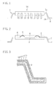
- FIG. 1 shows a semiconductor device 14 according to an embodiment of the present invention and FIG. 2 is a sectional view thereof. In FIG. 2, hatching is not provided for easy understanding of the structure.
- a lead frame 1 includes a die pad 3 provided in the middle thereof and inner leads 2 and outer leads 7 surrounding the die pad 3.
- the inner leads 2 and the outer leads 7 are connected, respectively.
- the inner leads 2 are electrically connected to electrode pads (not shown) of a semiconductor element 4 mounted on the die pad 3 via thin metal wires 5 and protected by a mold resin 6.
- Each of the outer leads 7 protruding from the side surface of the mold resin 6 includes two bends, i.e., a first bend 7a closer to the mold resin 6 and a second bend 7b. Part of the outer lead 7 covering from the second bend 7b to the tip of the outer lead 7 has a bottom surface called a mounting surface 8.
- the outer leads 7 are electrically connected to a printed circuit board (wiring board) 30 via solder paste 31 as shown in FIG. 9C.
- the outer leads 7 are arranged at a pitch of 500 ⁇ m and each of the outer leads 7 has a width of 250 ⁇ m.
- the lead pitch and the lead width are smaller than those disclosed by Japanese Unexamined Patent Publication No. H4-115558 .
- FIG. 3 is an enlarged sectional view of the outer lead 7.
- a 0.15 mm thick lead frame base 9 obtained by pressing or etching a copper alloy is plated through an electrolytic plating line.
- An underlayer plating 10 (nickel in the present embodiment) is formed as a first layer directly on the lead frame base 9, a palladium (Pd) plating 11 is formed thereon as a second layer, a silver (Ag) plating 12 is formed thereon as a third layer and a gold (Au) plating 13 is formed thereon as a fourth layer.
- the outer leads 7 are coated with a four-layer plating made of four different layers, and so are the inner leads 2.
- the four-layer plating improves wettability with lead free solder paste to a sufficient degree, though the three-layer plating disclosed by Japanese Unexamined Patent Publication No. H4-115558 does not when the lead pitch is reduced.
- explanation of the structure of the four-layer plating and suitable thicknesses of the four layers is provided.
- the underlayer plating 10 is a nickel plating not less than 0.2 ⁇ m and not more than 3.0 ⁇ m in thickness.
- the palladium plating 11 not less than 0.005 ⁇ m and not more than 0.2 ⁇ m in thickness
- the silver plating 12 not less than 0.05 ⁇ m and not more than 0.5 ⁇ m in thickness
- the gold plating 13 not less than 0.0015 ⁇ m and not more than 0.1 ⁇ m in thickness are formed in this order.
- the underlayer plating as the first layer is not limited to the nickel plating.
- the composition and thickness thereof may suitably be selected in consideration of resistance against corrosion of the lead frame base made of a copper alloy or the like, adhesion to the palladium plating as the second layer and cracking of the plating when the lead is bent.
- Ni and a Ni alloy are preferably used in a thickness of not less than 0.2 ⁇ m and not more than 3 ⁇ m. Taking characteristic and manufacturing cost into account, the thickness is more preferably not less than 0.5 ⁇ m and not more than 2 ⁇ m.
- the palladium plating as the second layer is provided to inhibit deposition of the underlayer plating and the thickness thereof is determined not to be too large for economical reasons. Therefore, the palladium plating is preferably not less than 0.05 ⁇ m and not more than 0.2 ⁇ m in thickness. If the thickness of the palladium plating is less than 0.05 ⁇ m, it is not preferable because the deposition of the underlayer plating becomes difficult to inhibit. On the other hand, if the thickness of the palladium plating is more than 0.2 ⁇ m, it is not preferable in terms of cost increase.
- the inventors have conducted various experiments to study the composition and the thickness thereof.
- the third plating plays an important role in determining the wettability with the solder paste and the quality of wire bonding.
- the inventors of the present invention have conducted measurement of the height of solder fillet lifted toward the outer leads. A greater solder fillet height means greater wicking characteristics.
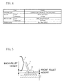
- the experiments were carried out using an actual implementation line under the conditions shown in FIG. 4 .
- FIG. 5 is a schematic view illustrating where the height of the solder fillet lifted toward the outer leads 7 was measured. Specifically, the height of front fillet generated at the tip of the outer lead 7 (the distance from the edge of the bottom surface of the outer lead 7 to the top end of the solder paste lifted upward to reach the end face of the outer lead 7) was measured and the height of back fillet generated around the second bend 7b (the distance from the edge of the bottom surface of the outer lead 7 to the top end of the solder paste lifted upward to reach a portion above the second bend 7b) was measured. Based on the measurement results, a comparison was made with a comparative three-layer plating made of an underlayer plating (nickel), a palladium plating and a gold plating.
- an underlayer plating nickel
- palladium plating palladium plating
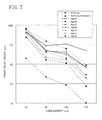
- FIGS. 6 and 7 are graphs illustrating the fillet height measurement results obtained with the four-layer plating of the present embodiment including a silver plating as the third layer and a gold plating as the fourth layer and the fillet height measurement results obtained with the comparative three-layer plating.
- the four-layer plating of the present embodiment showed apparent improvement in wettability with the solder.
- the four-layer plating of the present embodiment achieved higher wettability with the solder.
- the wicking characteristics were observed when the thickness of the silver plating was in the range of 0.02 to 0.2 ⁇ m.
- the thickness of the silver plating may be larger than 0.2 ⁇ m because the wettability hardly changes if the silver plating is formed thick.
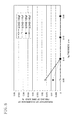
- FIG. 8 is a graph illustrating the evaluation results of reliability of thin metal wire connection established by the wire bonding. The evaluation was made for peeling of a joint between the metal wire and the inner lead. The graph shows that the silver plating not less than 0.1 ⁇ m in thickness always keeps the percentage of the occurrence of peeling of wire bond zero even if a bonding load is varied. This makes the bonding condition less severe and improves the connection reliability.
- the silver plating as the third layer is preferably not less than 0.05 ⁇ m in thickness, more preferably not less than 0.1 ⁇ m in thickness, at least in the inner leads 2.
- the silver plating as the third layer is not less than 0.05 ⁇ m and not more than 0.5 ⁇ m in thickness.
- the thickness is preferably not less than 0.1 ⁇ m and not more than 0.5 ⁇ m.
- the gold plating is configured to be not less than 0.0015 ⁇ m and not more than 0.1 ⁇ m in thickness almost for economical reasons. If the thickness of the gold plating is less than 0.0015 ⁇ m, it is not preferable because the wettability with the solder deteriorates. On the other hand, if the thickness of the gold plating is more than 0.1 ⁇ m thick, it is not preferable in terms of cost increase. The gold plating is more preferably not less than 0.003 ⁇ m and not more than 0.01 ⁇ m in thickness.
- the four-layer plating described above is formed on the lead frame. Therefore, even if the outer leads 7 are arranged at a pitch as small as 500 ⁇ m and each of the outer leads 7 has a width as small as 250 ⁇ m, the wettability with the solder paste is satisfactory, thereby obtaining high connection reliability. When the lead pitch and the lead width are reduced, the amount of the corresponding solder paste printed on the wiring board is reduced to deteriorate the reliability of the connection between the outer leads 7 and the wiring board. However, if the plating of the present embodiment is adopted, the connection reliability is kept high.
- the plating of the present embodiment makes it possible to maintain the high connection reliability between the wiring board with the solder paste printed thereon and the outer leads 7 as long as the pitch is 300 ⁇ m or more and the width is 80 ⁇ m or more.
- the above-described metallic plating is formed using four different plating baths.
- the semiconductor device assembly 14 shown in the figures which is a complete assembly, it is needless to say that adjacent layers in the four-layer plating are alloyed with each other due to thermal hysteresis of the assembling step. Therefore, it is possible to convert the thicknesses of the layers into the composition of the alloy, and vise versa.
- the lead frame 1 may be made of a copper alloy or an iron alloy which has been generally used for the semiconductor products and the thickness thereof is not particularly limited to 0.15 mm.
- Japanese Unexamined Patent Publication H4-115558 suggests the problem of migration of the sliver plating.
- a lead frame provided with the plating of the present embodiment and a comparative lead frame provided with a three-layer plating of Ni/Pd/Au (outermost layer) were examined for reliability under power supply voltage of 6V, temperature of 5 to 25°C and humidity of 60 to 90%. As a result, their reliabilities were equal and the migration did not occur.
- a metallic plating is provided with good wettability with lead free solder paste which is relatively poor in wicking characteristics.
- the present invention eliminates defect factors, such as solder joint open failure and failure in solder fillet formation.
Landscapes
- Lead Frames For Integrated Circuits (AREA)
Abstract
Description
- The present invention relates to a lead frame, in particular to a plated lead frame for use in semiconductor devices.
- According to reduction in size and weight of small products in recent years, there is a growing demand for reduction in size and thickness of semiconductor devices. Printed circuit boards for implementing the semiconductor devices are also required to be thin, small and multilayered. In general, the semiconductor device is implemented on the printed circuit board by reflowing.
- Hereinafter, explanation of problems involved in the step of reflowing the semiconductor device in a conventional manner is provided with reference to the drawings.
- FIGS. 9A, 9B and 9C show how a semiconductor device is implemented on a board. Here, a
semiconductor device 32 is prepared by mounting a semiconductor element on a lead frame and sealing it into a package with amold resin 33. - First, in a solder printing step shown in FIG. 9A,
solder paste 31 is applied onto electrode pads (not shown) provided on a printed circuit board (wiring board) 30. Then, in a mounting step shown in FIG. 9B, thesemiconductor device 32 is mounted on the printedcircuit board 30. Then, in a reflowing step shown in FIG. 9C, the whole device including the printedcircuit board 30 and thesemiconductor device 32 is heated at a high temperature to melt thesolder paste 31. Thesolder paste 31 is then cooled, thereby fixing and connecting thesemiconductor device 32 to theprint circuit board 30. - Through these steps,
outer leads 34 electrically conducted with electrode pads in the semiconductor element are electrically connected to the printedcircuit board 30 via thesolder paste 31. The bottommost surface of each of theouter leads 34 of thesemiconductor device 32 is generally called amounting surface 35. Theouter leads 34 are configured such thatcoplanarity 36 indicating flatness of themounting surface 35 as shown in FIG. 10 is in the range of several tens of µm. - In the reflowing step, the semiconductor device and the printed circuit board are deformed by various loads applied thereto while the temperature rises from a normal temperature of about 25°C to a high temperature of about 250°C. Specifically, the
semiconductor device 32 is deformed due to the difference in thermal expansion coefficient between theouter leads 34 principally made of iron or copper and themold resin 33. If thecoplanarity 36 is high, theouter leads 34 are deformed to be lifted above the printedcircuit board 30. - The printed
circuit board 30 which is made thin or multilayered is also deformed under the high temperature during the reflowing step. The deformation of these components synergistically causes defects, even if themounting surfaces 35 of theouter leads 34 are in contact with thesolder paste 31. For example, thesolder paste 31 does not achieve good wicking, i.e., solder fillet is not formed, or alternatively, theouter leads 34 are lifted above thesolder paste 31 to fail to establish electrical connection, thereby leading to solder joint open failure. - In order to prevent such defects, the surface of the lead frame is plated to improve wettability between the
outer leads 34 and thesolder paste 31. - In recent years, from the aspect of environment issues, lead free solder paste, such as SnAgCu, SnZn and SnAgBiIn, are used as the
solder paste 31 in many cases. However, the lead free solder pastes are poorer in wettability than conventional Sn-37%Pb eutectic solder and are likely to cause the defects such as the failure in solder fillet formation and the solder joint open failure. Therefore, a plating having good wettability with the lead free solder paste is required. - When the
outer leads 34 are coated with a SnPb eutectic plating having a relatively low melting point, the plating itself is molten under the high temperature condition during the reflowing step. Therefore, even if the lead free solder paste is used, the defect derived from the solder paste's lack of good wicking characteristics is less likely to occur. However, from the environmental standpoint, use of the Pb-containing plating will be restricted only in some very limited locations in electronic products. Thus, the plating of this kind is not available for general use. - When a lead free plating is used, e.g., a SnBi plating (a two-layer plating including a tin layer and a 2% Bi layer formed thereon), the SnBi plating itself is molten due to its low melting point just like the SnPb eutectic plating. Therefore, the problem of the solder paste's lack of good wicking characteristics does not occur.
- Further, when a palladium-based metallic plating which has been adopted as a lead free plating by many manufacturers is used (e.g., a three-layer plating of
nickel 20/palladium 24/gold 28 as shown in FIG. 11), the palladium-based metallic plating is not molten because its melting point is much higher than the high temperature condition during the reflowing step. However, the failure in solder fillet formation and the solder joint open failure have been less likely to occur even if the lead free solder paste is used. It is because the outer leads have been arranged at a pitch of 0.6 mm or more (e.g., seeJapanese Unexamined Patent Publication H4-115558 - In recent years, the semiconductor device and the wiring board have been fabricated under finer design rules. Accordingly, the area of connector lands has been reduced and the area of openings in a metal mask used for solder printing has also been reduced. As a result, the solder paste does not easily come off the openings of the printing mask, thereby causing lack of the solder paste on the wiring board. Even if the printing succeeds, the total amount of the solder printed on the minuscule regions is smaller than it used to be. With the trend toward the smaller pitch, in particular when the pitch of the outer leads is reduced to less than 0.6 mm, the plated outer leads as disclosed by
Japanese Unexamined Patent Publication H4-115558 - Further, while the outer leads are plated with SnBi, the inner leads are plated by Ag spot plating. This brings about considerable increase in manufacturing cost.
- The present invention has been achieved under these circumstances. An object of the present invention is to provide a lead frame coated with a plating which ensures the wettability of the lead frame and the lead free solder even if the outer lead pitch is reduced.
- The lead frame of the present invention includes a die pad for mounting a semiconductor element thereon, inner leads electrically connected to electrode pads of the semiconductor element and outer leads connected to the inner leads to function as external terminals, wherein at least the ends of the outer leads opposite to the inner leads are coated with a four-layer plating, first three layers in the four-layer plating from the topmost surface thereof are made of Au, Ag and Pd, respectively, and the Ag layer is not less than 0.05 µm and not more than 0.5 µm in thickness.
- It is preferred that the outer leads are arranged at a pitch of not less than 300 µm and not more than 500 µm.
- It is preferred that each of the outer leads is not less than 80 µm and not more than 250 µm in width.
- It is preferred that the Pd layer in the four-layer plating is not less than 0.005 µm and not more than 0.2 µm in thickness.
- It is preferred that the Au layer in the four-layer plating not less than 0.0015 µm and not more than 0.1 µm in thickness.
- It is preferred that the lead frame is made of Cu or Fe.
- It is preferred that the four-layer plating includes a Ni layer as an undermost layer.
- It is preferred that the Ni layer in the four-layer plating is not less than 0.2 µm and not more than 3.0 µm in thickness.
-
- FIG. 1 is a schematic side view of a semiconductor device using a lead frame according to the present invention.
- FIG. 2 is a schematic sectional view of the semiconductor device using the lead frame according to the present invention.
- FIG. 3 is a schematic sectional view of an outer lead of the lead frame according to the present invention.
- FIG. 4 is a table showing the conditions of an implementation experiment.
- FIG. 5 is a schematic view illustrating where the height of solder fillet is measured.
- FIG. 6 is a graph illustrating a comparison between the height of back fillet of an embodiment of the invention and that of a comparative embodiment.
- FIG. 7 is a graph illustrating a comparison between the height of front fillet of the embodiment of the invention and that of the comparative embodiment.
- FIG. 8 is a graph illustrating the evaluation results of connection reliability after a wire bonding step.
- FIGS. 9A to 9C are views illustrating how a semiconductor device is implemented on a board.
- FIG. 10 is a side view of a semiconductor device.
- FIG. 11 is a schematic sectional view illustrating the structure of a plating provided on a lead frame in a conventional manner.
- Hereinafter, explanation of an embodiment of the present invention is provided with reference to the drawings. In the drawings, components having substantially the same function are indicated by the same reference numeral for simple explanation.
- FIG. 1 shows a
semiconductor device 14 according to an embodiment of the present invention and FIG. 2 is a sectional view thereof. In FIG. 2, hatching is not provided for easy understanding of the structure. - A lead frame 1 includes a die pad 3 provided in the middle thereof and
inner leads 2 andouter leads 7 surrounding the die pad 3. The inner leads 2 and the outer leads 7 are connected, respectively. The inner leads 2 are electrically connected to electrode pads (not shown) of asemiconductor element 4 mounted on the die pad 3 viathin metal wires 5 and protected by amold resin 6. Each of the outer leads 7 protruding from the side surface of themold resin 6 includes two bends, i.e., afirst bend 7a closer to themold resin 6 and asecond bend 7b. Part of theouter lead 7 covering from thesecond bend 7b to the tip of theouter lead 7 has a bottom surface called a mounting surface 8. The outer leads 7 are electrically connected to a printed circuit board (wiring board) 30 viasolder paste 31 as shown in FIG. 9C. - In the present embodiment, the outer leads 7 are arranged at a pitch of 500 µm and each of the outer leads 7 has a width of 250 µm. The lead pitch and the lead width are smaller than those disclosed by
Japanese Unexamined Patent Publication No. H4-115558 - FIG. 3 is an enlarged sectional view of the
outer lead 7. In thelead frame 7 of the present embodiment, a 0.15 mm thicklead frame base 9 obtained by pressing or etching a copper alloy is plated through an electrolytic plating line. An underlayer plating 10 (nickel in the present embodiment) is formed as a first layer directly on thelead frame base 9, a palladium (Pd) plating 11 is formed thereon as a second layer, a silver (Ag) plating 12 is formed thereon as a third layer and a gold (Au) plating 13 is formed thereon as a fourth layer. Thus, the outer leads 7 are coated with a four-layer plating made of four different layers, and so are the inner leads 2. The four-layer plating improves wettability with lead free solder paste to a sufficient degree, though the three-layer plating disclosed byJapanese Unexamined Patent Publication No. H4-115558 - The underlayer plating 10 is a nickel plating not less than 0.2 µm and not more than 3.0 µm in thickness. On the nickel coating, the palladium plating 11 not less than 0.005 µm and not more than 0.2 µm in thickness, the silver plating 12 not less than 0.05 µm and not more than 0.5 µm in thickness and the gold plating 13 not less than 0.0015 µm and not more than 0.1 µm in thickness are formed in this order.
- Detailed explanation of the four platings is provided below.
- The underlayer plating as the first layer is not limited to the nickel plating. The composition and thickness thereof may suitably be selected in consideration of resistance against corrosion of the lead frame base made of a copper alloy or the like, adhesion to the palladium plating as the second layer and cracking of the plating when the lead is bent. From the past experience, Ni and a Ni alloy are preferably used in a thickness of not less than 0.2 µm and not more than 3 µm. Taking characteristic and manufacturing cost into account, the thickness is more preferably not less than 0.5 µm and not more than 2 µm.
- The palladium plating as the second layer is provided to inhibit deposition of the underlayer plating and the thickness thereof is determined not to be too large for economical reasons. Therefore, the palladium plating is preferably not less than 0.05 µm and not more than 0.2 µm in thickness. If the thickness of the palladium plating is less than 0.05 µm, it is not preferable because the deposition of the underlayer plating becomes difficult to inhibit. On the other hand, if the thickness of the palladium plating is more than 0.2 µm, it is not preferable in terms of cost increase.
- As to the third plating, the inventors have conducted various experiments to study the composition and the thickness thereof. The third plating plays an important role in determining the wettability with the solder paste and the quality of wire bonding. As an index of good wicking characteristics of the lead free solder paste, which is of great concern in the art, the inventors of the present invention have conducted measurement of the height of solder fillet lifted toward the outer leads. A greater solder fillet height means greater wicking characteristics. The experiments were carried out using an actual implementation line under the conditions shown in FIG. 4.
- FIG. 5 is a schematic view illustrating where the height of the solder fillet lifted toward the outer leads 7 was measured. Specifically, the height of front fillet generated at the tip of the outer lead 7 (the distance from the edge of the bottom surface of the
outer lead 7 to the top end of the solder paste lifted upward to reach the end face of the outer lead 7) was measured and the height of back fillet generated around thesecond bend 7b (the distance from the edge of the bottom surface of theouter lead 7 to the top end of the solder paste lifted upward to reach a portion above thesecond bend 7b) was measured. Based on the measurement results, a comparison was made with a comparative three-layer plating made of an underlayer plating (nickel), a palladium plating and a gold plating. - FIGS. 6 and 7 are graphs illustrating the fillet height measurement results obtained with the four-layer plating of the present embodiment including a silver plating as the third layer and a gold plating as the fourth layer and the fillet height measurement results obtained with the comparative three-layer plating. As compared with the comparative three-layer plating, the four-layer plating of the present embodiment showed apparent improvement in wettability with the solder. In particular, as compared with a combination of the three-layer plating and the lead-containing solder paste, the four-layer plating of the present embodiment achieved higher wettability with the solder. Further, the wicking characteristics were observed when the thickness of the silver plating was in the range of 0.02 to 0.2 µm. The thickness of the silver plating may be larger than 0.2 µm because the wettability hardly changes if the silver plating is formed thick.
- From the viewpoint of a wire bonding step which is one of the steps for assembling the semiconductor device, it has been found that a thick silver plating makes it possible to improve the reliability of connection established by wire bonding. FIG. 8 is a graph illustrating the evaluation results of reliability of thin metal wire connection established by the wire bonding. The evaluation was made for peeling of a joint between the metal wire and the inner lead. The graph shows that the silver plating not less than 0.1 µm in thickness always keeps the percentage of the occurrence of peeling of wire bond zero even if a bonding load is varied. This makes the bonding condition less severe and improves the connection reliability. Even if the silver plating is 0.05 µm thick, the percentage of the occurrence of peeling of wire bond is low enough to make the bonding condition less severe and improve the connection reliability to a practical degree. In short, the silver plating as the third layer is preferably not less than 0.05 µm in thickness, more preferably not less than 0.1 µm in thickness, at least in the inner leads 2.
- Taking the experimental results and the manufacturing cost into account, it is preferred that the silver plating as the third layer is not less than 0.05 µm and not more than 0.5 µm in thickness. From the viewpoint of the wire bonding, the thickness is preferably not less than 0.1 µm and not more than 0.5 µm.
- Finally, a study of the gold plating as the fourth layer has been made. The gold plating is configured to be not less than 0.0015 µm and not more than 0.1 µm in thickness almost for economical reasons. If the thickness of the gold plating is less than 0.0015 µm, it is not preferable because the wettability with the solder deteriorates. On the other hand, if the thickness of the gold plating is more than 0.1 µm thick, it is not preferable in terms of cost increase. The gold plating is more preferably not less than 0.003 µm and not more than 0.01 µm in thickness.
- In the present embodiment, the four-layer plating described above is formed on the lead frame. Therefore, even if the outer leads 7 are arranged at a pitch as small as 500 µm and each of the outer leads 7 has a width as small as 250 µm, the wettability with the solder paste is satisfactory, thereby obtaining high connection reliability. When the lead pitch and the lead width are reduced, the amount of the corresponding solder paste printed on the wiring board is reduced to deteriorate the reliability of the connection between the
outer leads 7 and the wiring board. However, if the plating of the present embodiment is adopted, the connection reliability is kept high. As a result of study on the lead pitch and the lead width of the outer leads 7, it is found that the plating of the present embodiment makes it possible to maintain the high connection reliability between the wiring board with the solder paste printed thereon and the outer leads 7 as long as the pitch is 300 µm or more and the width is 80 µm or more. - The above-described metallic plating is formed using four different plating baths. Referring to the
semiconductor device assembly 14 shown in the figures which is a complete assembly, it is needless to say that adjacent layers in the four-layer plating are alloyed with each other due to thermal hysteresis of the assembling step. Therefore, it is possible to convert the thicknesses of the layers into the composition of the alloy, and vise versa. The lead frame 1 may be made of a copper alloy or an iron alloy which has been generally used for the semiconductor products and the thickness thereof is not particularly limited to 0.15 mm. -
Japanese Unexamined Patent Publication H4-115558 - According to the present invention, a metallic plating is provided with good wettability with lead free solder paste which is relatively poor in wicking characteristics. Thus, the present invention eliminates defect factors, such as solder joint open failure and failure in solder fillet formation.
Claims (8)
- A lead frame (1) comprising a die pad (3) for mounting a semiconductor element (4) thereon, inner leads (2) electrically connected to electrode pads of the semiconductor element (4) and outer leads (7) connected to the inner leads (2) to function as external terminals, wherein
at least the ends of the outer leads (7) opposite to the inner leads (2) are coated with a four-layer plating,
first three layers in the four-layer plating from the topmost surface thereof are made of Au, Ag and Pd, respectively, and
the Ag layer (12) is not less than 0.05 µm and not more than 0.5 µm in thickness. - The lead frame of Claim 1, wherein
the outer leads (7) are arranged at a pitch of not less than 300 µm and not more than 500 µm. - The lead frame of Claim 1 or 2, wherein
each of the outer leads (7) is not less than 80 µm and not more than 250 µm in width. - The lead frame of any one of Claims 1 to 3, wherein
the Pd layer (11) in the four-layer plating is not less than 0.005 µm and not more than 0.2 µm in thickness. - The lead frame of any one of Claims 1 to 4, wherein
the Au layer (13) in the four-layer plating is not less than 0.0015 µm and not more than 0.1 µm in thickness. - The lead frame of Claim 1, wherein
the lead frame (1) is made of Cu or Fe. - The lead frame of Claim 1, wherein
the four-layer plating includes a Ni layer as an undermost layer (10). - The lead frame of Claim 7, wherein
the Ni layer in the four-layer plating is not less than 0.2 µm and not more than 3.0 µm in thickness.
Applications Claiming Priority (1)
| Application Number | Priority Date | Filing Date | Title |
|---|---|---|---|
| JP2005306379A JP4820616B2 (en) | 2005-10-20 | 2005-10-20 | Lead frame |
Publications (2)
| Publication Number | Publication Date |
|---|---|
| EP1777743A2 true EP1777743A2 (en) | 2007-04-25 |
| EP1777743A3 EP1777743A3 (en) | 2008-11-19 |
Family
ID=37719312
Family Applications (1)
| Application Number | Title | Priority Date | Filing Date |
|---|---|---|---|
| EP06122491A Ceased EP1777743A3 (en) | 2005-10-20 | 2006-10-18 | Lead frame |
Country Status (5)
| Country | Link |
|---|---|
| US (1) | US8283759B2 (en) |
| EP (1) | EP1777743A3 (en) |
| JP (1) | JP4820616B2 (en) |
| CN (1) | CN1953168B (en) |
| TW (1) | TW200717729A (en) |
Families Citing this family (7)
| Publication number | Priority date | Publication date | Assignee | Title |
|---|---|---|---|---|
| DE102006032074B3 (en) * | 2006-07-11 | 2007-12-27 | Infineon Technologies Ag | Connecting lead for use in e.g. semiconductor component, has connecting regions for connecting two work pieces respectively, where nickel-phosphorus layer on nickel layer is formed in one of connecting regions |
| WO2009008526A1 (en) | 2007-07-06 | 2009-01-15 | Ddk Ltd. | Process for producing electronic component, and electronic component produced by the process |
| JP5762081B2 (en) * | 2011-03-29 | 2015-08-12 | 新光電気工業株式会社 | Lead frame and semiconductor device |
| CN105018995A (en) * | 2015-07-10 | 2015-11-04 | 陈圳浩 | Silver ornament surface brightness five-layer electroplating technology |
| CN115602653A (en) * | 2021-06-28 | 2023-01-13 | 上海凯虹科技电子有限公司(Cn) | Lead frame and semiconductor device |
| CN117089838A (en) * | 2022-05-19 | 2023-11-21 | 泰连解决方案有限责任公司 | Layered plating stacks for improved contact resistance in corrosive environments |
| US12351936B2 (en) * | 2022-05-19 | 2025-07-08 | Te Connectivity Solutions Gmbh | Layered plating stack for improved contact resistance in corrosive environments |
Citations (2)
| Publication number | Priority date | Publication date | Assignee | Title |
|---|---|---|---|---|
| JPH04115558A (en) | 1990-09-05 | 1992-04-16 | Shinko Electric Ind Co Ltd | Lead frame for semiconductor device |
| US20030011048A1 (en) | 1999-03-19 | 2003-01-16 | Abbott Donald C. | Semiconductor circuit assembly having a plated leadframe including gold selectively covering areas to be soldered |
Family Cites Families (23)
| Publication number | Priority date | Publication date | Assignee | Title |
|---|---|---|---|---|
| DE68923024T2 (en) * | 1988-03-28 | 1995-11-02 | Texas Instruments Inc | Lead frame with reduced corrosion. |
| US5014113A (en) * | 1989-12-27 | 1991-05-07 | Motorola, Inc. | Multiple layer lead frame |
| JPH04337657A (en) | 1991-05-14 | 1992-11-25 | Hitachi Cable Ltd | Lead frame for semiconductor device |
| US5360991A (en) * | 1993-07-29 | 1994-11-01 | At&T Bell Laboratories | Integrated circuit devices with solderable lead frame |
| US5650661A (en) * | 1993-12-27 | 1997-07-22 | National Semiconductor Corporation | Protective coating combination for lead frames |
| US5436082A (en) * | 1993-12-27 | 1995-07-25 | National Semiconductor Corporation | Protective coating combination for lead frames |
| JP3550875B2 (en) | 1996-05-14 | 2004-08-04 | ソニー株式会社 | Lead frame and semiconductor device using the same |
| JPH1074879A (en) | 1996-08-30 | 1998-03-17 | Mitsui High Tec Inc | Lead frame for semiconductor device |
| KR100231828B1 (en) * | 1997-02-20 | 1999-12-01 | 유무성 | Multi-layer plated lead frame |
| US5994767A (en) * | 1997-04-09 | 1999-11-30 | Sitron Precision Co., Ltd. | Leadframe for integrated circuit package and method of manufacturing the same |
| DE19850526C2 (en) * | 1998-11-03 | 2002-11-28 | Heraeus Gmbh W C | Metallic coating substrate and its use |
| DE59900741D1 (en) * | 1998-06-10 | 2002-02-28 | Heraeus Gmbh W C | METHOD FOR PRODUCING A LEAD-FREE SUBSTRATE |
| JP2001230360A (en) * | 2000-02-18 | 2001-08-24 | Hitachi Ltd | Semiconductor integrated circuit device and method of manufacturing the same |
| JP2002076229A (en) | 2000-07-13 | 2002-03-15 | Texas Instruments Inc | Semiconductor lead frame including silver plating and method of manufacturing the same |
| KR100371567B1 (en) * | 2000-12-08 | 2003-02-07 | 삼성테크윈 주식회사 | Ag pre-plated lead frame for semiconductor package |
| JP2003198117A (en) * | 2001-12-28 | 2003-07-11 | Matsushita Electric Ind Co Ltd | Soldering method and joint structure |
| JP3519726B1 (en) * | 2002-11-26 | 2004-04-19 | Fcm株式会社 | Terminal and parts having it |
| KR101059361B1 (en) * | 2003-01-16 | 2011-08-24 | 파나소닉 주식회사 | Lead frame and semiconductor light emitting device |
| JP2004241542A (en) * | 2003-02-05 | 2004-08-26 | Matsushita Electric Ind Co Ltd | Soldering method, parts joined by the soldering method, and joined joint structure |
| JP2005019922A (en) | 2003-06-30 | 2005-01-20 | Shinko Electric Ind Co Ltd | Lead frame for semiconductor packages |
| KR100998042B1 (en) * | 2004-02-23 | 2010-12-03 | 삼성테크윈 주식회사 | Lead frame and manufacturing method of semiconductor package having same |
| WO2005117112A1 (en) * | 2004-05-27 | 2005-12-08 | Shinko Electric Industries Co., Ltd. | Lead frame for semiconductor device |
| JP2006269903A (en) * | 2005-03-25 | 2006-10-05 | Shinko Electric Ind Co Ltd | Lead frame for semiconductor devices |
-
2005
- 2005-10-20 JP JP2005306379A patent/JP4820616B2/en not_active Expired - Lifetime
-
2006
- 2006-10-18 CN CN2006101356292A patent/CN1953168B/en active Active
- 2006-10-18 EP EP06122491A patent/EP1777743A3/en not_active Ceased
- 2006-10-19 US US11/582,972 patent/US8283759B2/en active Active
- 2006-10-20 TW TW095138819A patent/TW200717729A/en unknown
Patent Citations (2)
| Publication number | Priority date | Publication date | Assignee | Title |
|---|---|---|---|---|
| JPH04115558A (en) | 1990-09-05 | 1992-04-16 | Shinko Electric Ind Co Ltd | Lead frame for semiconductor device |
| US20030011048A1 (en) | 1999-03-19 | 2003-01-16 | Abbott Donald C. | Semiconductor circuit assembly having a plated leadframe including gold selectively covering areas to be soldered |
Also Published As
| Publication number | Publication date |
|---|---|
| US20070090501A1 (en) | 2007-04-26 |
| JP4820616B2 (en) | 2011-11-24 |
| EP1777743A3 (en) | 2008-11-19 |
| TW200717729A (en) | 2007-05-01 |
| US8283759B2 (en) | 2012-10-09 |
| CN1953168B (en) | 2010-07-28 |
| CN1953168A (en) | 2007-04-25 |
| JP2007115925A (en) | 2007-05-10 |
Similar Documents
| Publication | Publication Date | Title |
|---|---|---|
| US8069558B2 (en) | Method for manufacturing substrate having built-in components | |
| KR100750012B1 (en) | Semiconductor integrated circuit device | |
| US6093964A (en) | Connection structure utilizing a metal bump and metal bump manufacturing method | |
| CN111418272B (en) | Flexible printed circuit board and method of manufacturing flexible printed circuit board | |
| US20090146316A1 (en) | Flip-chip assembly with organic chip carrier having mushroom-plated solder resist opening | |
| KR20020035774A (en) | Electronic components, method and structure for mounting semiconductor device | |
| KR20040012877A (en) | Semiconductor device and its production method | |
| JP2006222406A (en) | Semiconductor device | |
| CN101339935A (en) | Connection structure between printed circuit board and electronic components | |
| CN1206887C (en) | Printed circuit assembly | |
| JPH11350189A (en) | Materials for electric / electronic parts, methods of manufacturing the same, and electric / electronic parts using the materials | |
| US8283759B2 (en) | Lead frame having outer leads coated with a four layer plating | |
| US20080157359A1 (en) | Crack-resistant solder joint, electronic component such as circuit substrate having the solder joint, semiconductor device, and manufacturing method of electronic component | |
| EP1307076A1 (en) | Structure for interconnecting conductors and connecting method | |
| US5877543A (en) | Device assembly structure with reinforced outer leads | |
| JPH11350190A (en) | Materials for electric / electronic parts, methods of manufacturing the same, and electric / electronic parts using the materials | |
| JPH1093004A (en) | Electronic component and method of manufacturing the same | |
| KR100591235B1 (en) | Semiconductor device | |
| JPH11343594A (en) | Material for electric / electronic parts, method of manufacturing the same, and electric / electronic parts using the same | |
| JP3969991B2 (en) | Surface mount electronic components | |
| US7701061B2 (en) | Semiconductor device with solder balls having high reliability | |
| JPH08316641A (en) | Multi-layer wiring board by batch connection method | |
| JPH10313087A (en) | Lead materials for electronic components | |
| JPS6258548B2 (en) | ||
| CN113556883A (en) | Preparation method of circuit board packaging structure and circuit board packaging structure |
Legal Events
| Date | Code | Title | Description |
|---|---|---|---|
| PUAI | Public reference made under article 153(3) epc to a published international application that has entered the european phase |
Free format text: ORIGINAL CODE: 0009012 |
|
| AK | Designated contracting states |
Kind code of ref document: A2 Designated state(s): AT BE BG CH CY CZ DE DK EE ES FI FR GB GR HU IE IS IT LI LT LU LV MC NL PL PT RO SE SI SK TR |
|
| AX | Request for extension of the european patent |
Extension state: AL BA HR MK YU |
|
| PUAL | Search report despatched |
Free format text: ORIGINAL CODE: 0009013 |
|
| AK | Designated contracting states |
Kind code of ref document: A3 Designated state(s): AT BE BG CH CY CZ DE DK EE ES FI FR GB GR HU IE IS IT LI LT LU LV MC NL PL PT RO SE SI SK TR |
|
| AX | Request for extension of the european patent |
Extension state: AL BA HR MK RS |
|
| RAP1 | Party data changed (applicant data changed or rights of an application transferred) |
Owner name: SHINKO ELECTRIC INDUSTRIES CO., LTD. Owner name: PANASONIC CORPORATION |
|
| 17P | Request for examination filed |
Effective date: 20090331 |
|
| 17Q | First examination report despatched |
Effective date: 20090507 |
|
| AKX | Designation fees paid |
Designated state(s): DE FR IT |
|
| STAA | Information on the status of an ep patent application or granted ep patent |
Free format text: STATUS: THE APPLICATION HAS BEEN REFUSED |
|
| 18R | Application refused |
Effective date: 20131227 |