EP1772907A2 - Germanium-Solarzelle und Verfahren zu ihrer Herstellung - Google Patents
Germanium-Solarzelle und Verfahren zu ihrer Herstellung Download PDFInfo
- Publication number
- EP1772907A2 EP1772907A2 EP06121983A EP06121983A EP1772907A2 EP 1772907 A2 EP1772907 A2 EP 1772907A2 EP 06121983 A EP06121983 A EP 06121983A EP 06121983 A EP06121983 A EP 06121983A EP 1772907 A2 EP1772907 A2 EP 1772907A2
- Authority
- EP
- European Patent Office
- Prior art keywords
- layer
- passivation layer
- contact
- substrate
- contacting
- Prior art date
- Legal status (The legal status is an assumption and is not a legal conclusion. Google has not performed a legal analysis and makes no representation as to the accuracy of the status listed.)
- Withdrawn
Links
- 229910052732 germanium Inorganic materials 0.000 title claims abstract description 91
- GNPVGFCGXDBREM-UHFFFAOYSA-N germanium atom Chemical compound [Ge] GNPVGFCGXDBREM-UHFFFAOYSA-N 0.000 title claims abstract description 90
- 238000000034 method Methods 0.000 title claims abstract description 70
- 238000004519 manufacturing process Methods 0.000 title description 7
- 238000002161 passivation Methods 0.000 claims abstract description 133
- 239000000758 substrate Substances 0.000 claims abstract description 92
- 229910052751 metal Inorganic materials 0.000 claims abstract description 78
- 239000002184 metal Substances 0.000 claims abstract description 78
- 229910021417 amorphous silicon Inorganic materials 0.000 claims abstract description 46
- KDLHZDBZIXYQEI-UHFFFAOYSA-N Palladium Chemical compound [Pd] KDLHZDBZIXYQEI-UHFFFAOYSA-N 0.000 claims abstract description 44
- 238000010438 heat treatment Methods 0.000 claims abstract description 36
- 229910052782 aluminium Inorganic materials 0.000 claims abstract description 35
- XAGFODPZIPBFFR-UHFFFAOYSA-N aluminium Chemical compound [Al] XAGFODPZIPBFFR-UHFFFAOYSA-N 0.000 claims abstract description 34
- 239000004411 aluminium Substances 0.000 claims abstract description 33
- 239000002210 silicon-based material Substances 0.000 claims abstract description 25
- 239000010949 copper Substances 0.000 claims abstract description 22
- 229910052763 palladium Inorganic materials 0.000 claims abstract description 21
- 229910052802 copper Inorganic materials 0.000 claims abstract description 17
- RYGMFSIKBFXOCR-UHFFFAOYSA-N Copper Chemical compound [Cu] RYGMFSIKBFXOCR-UHFFFAOYSA-N 0.000 claims abstract description 7
- 238000000623 plasma-assisted chemical vapour deposition Methods 0.000 claims description 26
- 229910052709 silver Inorganic materials 0.000 claims description 22
- 238000000151 deposition Methods 0.000 claims description 21
- 239000010931 gold Substances 0.000 claims description 20
- 238000004140 cleaning Methods 0.000 claims description 18
- 229910052737 gold Inorganic materials 0.000 claims description 17
- 230000004888 barrier function Effects 0.000 claims description 16
- 239000004020 conductor Substances 0.000 claims description 12
- 230000008021 deposition Effects 0.000 claims description 12
- VYPSYNLAJGMNEJ-UHFFFAOYSA-N Silicium dioxide Chemical compound O=[Si]=O VYPSYNLAJGMNEJ-UHFFFAOYSA-N 0.000 claims description 11
- 239000010944 silver (metal) Substances 0.000 claims description 10
- BQCADISMDOOEFD-UHFFFAOYSA-N Silver Chemical compound [Ag] BQCADISMDOOEFD-UHFFFAOYSA-N 0.000 claims description 9
- 239000004332 silver Substances 0.000 claims description 9
- 229910020776 SixNy Inorganic materials 0.000 claims description 5
- PCHJSUWPFVWCPO-UHFFFAOYSA-N gold Chemical compound [Au] PCHJSUWPFVWCPO-UHFFFAOYSA-N 0.000 claims description 5
- 239000002923 metal particle Substances 0.000 claims description 5
- 229910052814 silicon oxide Inorganic materials 0.000 claims description 5
- 238000005334 plasma enhanced chemical vapour deposition Methods 0.000 claims description 3
- 239000010410 layer Substances 0.000 description 276
- 238000009792 diffusion process Methods 0.000 description 38
- 239000007789 gas Substances 0.000 description 12
- 239000005083 Zinc sulfide Substances 0.000 description 10
- 229910052984 zinc sulfide Inorganic materials 0.000 description 10
- 229940063789 zinc sulfide Drugs 0.000 description 10
- 239000000463 material Substances 0.000 description 9
- 238000010304 firing Methods 0.000 description 8
- 230000008569 process Effects 0.000 description 7
- 239000000126 substance Substances 0.000 description 7
- 238000000137 annealing Methods 0.000 description 6
- 230000008020 evaporation Effects 0.000 description 6
- 238000001704 evaporation Methods 0.000 description 6
- 238000005259 measurement Methods 0.000 description 6
- 239000006117 anti-reflective coating Substances 0.000 description 5
- 230000006870 function Effects 0.000 description 5
- 230000006872 improvement Effects 0.000 description 5
- ORUIBWPALBXDOA-UHFFFAOYSA-L magnesium fluoride Chemical compound [F-].[F-].[Mg+2] ORUIBWPALBXDOA-UHFFFAOYSA-L 0.000 description 5
- 229910001635 magnesium fluoride Inorganic materials 0.000 description 5
- 230000006798 recombination Effects 0.000 description 5
- 238000005215 recombination Methods 0.000 description 5
- 238000011282 treatment Methods 0.000 description 5
- 235000012431 wafers Nutrition 0.000 description 5
- 239000000203 mixture Substances 0.000 description 4
- 230000004044 response Effects 0.000 description 4
- 238000001228 spectrum Methods 0.000 description 4
- 229910052581 Si3N4 Inorganic materials 0.000 description 3
- 230000015572 biosynthetic process Effects 0.000 description 3
- 229910052681 coesite Inorganic materials 0.000 description 3
- 229910052906 cristobalite Inorganic materials 0.000 description 3
- 230000000694 effects Effects 0.000 description 3
- 238000009713 electroplating Methods 0.000 description 3
- 238000005530 etching Methods 0.000 description 3
- BHEPBYXIRTUNPN-UHFFFAOYSA-N hydridophosphorus(.) (triplet) Chemical compound [PH] BHEPBYXIRTUNPN-UHFFFAOYSA-N 0.000 description 3
- 238000012986 modification Methods 0.000 description 3
- 230000004048 modification Effects 0.000 description 3
- 230000005855 radiation Effects 0.000 description 3
- 239000000377 silicon dioxide Substances 0.000 description 3
- 229910052682 stishovite Inorganic materials 0.000 description 3
- 229910052905 tridymite Inorganic materials 0.000 description 3
- BLRPTPMANUNPDV-UHFFFAOYSA-N Silane Chemical compound [SiH4] BLRPTPMANUNPDV-UHFFFAOYSA-N 0.000 description 2
- 230000003667 anti-reflective effect Effects 0.000 description 2
- 238000010420 art technique Methods 0.000 description 2
- 230000003247 decreasing effect Effects 0.000 description 2
- 239000002019 doping agent Substances 0.000 description 2
- 239000002355 dual-layer Substances 0.000 description 2
- 239000006023 eutectic alloy Substances 0.000 description 2
- 150000002739 metals Chemical class 0.000 description 2
- 238000005457 optimization Methods 0.000 description 2
- 238000000059 patterning Methods 0.000 description 2
- 238000002310 reflectometry Methods 0.000 description 2
- 238000004088 simulation Methods 0.000 description 2
- 238000012546 transfer Methods 0.000 description 2
- UFHFLCQGNIYNRP-UHFFFAOYSA-N Hydrogen Chemical compound [H][H] UFHFLCQGNIYNRP-UHFFFAOYSA-N 0.000 description 1
- 229910008310 Si—Ge Inorganic materials 0.000 description 1
- OFLYIWITHZJFLS-UHFFFAOYSA-N [Si].[Au] Chemical compound [Si].[Au] OFLYIWITHZJFLS-UHFFFAOYSA-N 0.000 description 1
- XNRNVYYTHRPBDD-UHFFFAOYSA-N [Si][Ag] Chemical compound [Si][Ag] XNRNVYYTHRPBDD-UHFFFAOYSA-N 0.000 description 1
- 238000010521 absorption reaction Methods 0.000 description 1
- 230000004075 alteration Effects 0.000 description 1
- 230000005540 biological transmission Effects 0.000 description 1
- 230000008859 change Effects 0.000 description 1
- 239000011248 coating agent Substances 0.000 description 1
- 238000000576 coating method Methods 0.000 description 1
- 238000013461 design Methods 0.000 description 1
- 229910003460 diamond Inorganic materials 0.000 description 1
- 239000010432 diamond Substances 0.000 description 1
- -1 for example Substances 0.000 description 1
- 150000002290 germanium Chemical class 0.000 description 1
- 230000005484 gravity Effects 0.000 description 1
- 239000001257 hydrogen Substances 0.000 description 1
- 229910052739 hydrogen Inorganic materials 0.000 description 1
- 238000005286 illumination Methods 0.000 description 1
- 238000013532 laser treatment Methods 0.000 description 1
- 230000000873 masking effect Effects 0.000 description 1
- 230000008450 motivation Effects 0.000 description 1
- 238000002203 pretreatment Methods 0.000 description 1
- 238000012545 processing Methods 0.000 description 1
- 230000003595 spectral effect Effects 0.000 description 1
- 238000004528 spin coating Methods 0.000 description 1
- 238000012360 testing method Methods 0.000 description 1
- DRDVZXDWVBGGMH-UHFFFAOYSA-N zinc;sulfide Chemical compound [S-2].[Zn+2] DRDVZXDWVBGGMH-UHFFFAOYSA-N 0.000 description 1
Images


Classifications
-
- H—ELECTRICITY
- H01—ELECTRIC ELEMENTS
- H01L—SEMICONDUCTOR DEVICES NOT COVERED BY CLASS H10
- H01L31/00—Semiconductor devices sensitive to infrared radiation, light, electromagnetic radiation of shorter wavelength or corpuscular radiation and specially adapted either for the conversion of the energy of such radiation into electrical energy or for the control of electrical energy by such radiation; Processes or apparatus specially adapted for the manufacture or treatment thereof or of parts thereof; Details thereof
- H01L31/02—Details
- H01L31/0224—Electrodes
- H01L31/022408—Electrodes for devices characterised by at least one potential jump barrier or surface barrier
- H01L31/022425—Electrodes for devices characterised by at least one potential jump barrier or surface barrier for solar cells
-
- H—ELECTRICITY
- H01—ELECTRIC ELEMENTS
- H01L—SEMICONDUCTOR DEVICES NOT COVERED BY CLASS H10
- H01L31/00—Semiconductor devices sensitive to infrared radiation, light, electromagnetic radiation of shorter wavelength or corpuscular radiation and specially adapted either for the conversion of the energy of such radiation into electrical energy or for the control of electrical energy by such radiation; Processes or apparatus specially adapted for the manufacture or treatment thereof or of parts thereof; Details thereof
- H01L31/02—Details
- H01L31/0216—Coatings
- H01L31/02161—Coatings for devices characterised by at least one potential jump barrier or surface barrier
- H01L31/02167—Coatings for devices characterised by at least one potential jump barrier or surface barrier for solar cells
-
- H—ELECTRICITY
- H01—ELECTRIC ELEMENTS
- H01L—SEMICONDUCTOR DEVICES NOT COVERED BY CLASS H10
- H01L31/00—Semiconductor devices sensitive to infrared radiation, light, electromagnetic radiation of shorter wavelength or corpuscular radiation and specially adapted either for the conversion of the energy of such radiation into electrical energy or for the control of electrical energy by such radiation; Processes or apparatus specially adapted for the manufacture or treatment thereof or of parts thereof; Details thereof
- H01L31/0248—Semiconductor devices sensitive to infrared radiation, light, electromagnetic radiation of shorter wavelength or corpuscular radiation and specially adapted either for the conversion of the energy of such radiation into electrical energy or for the control of electrical energy by such radiation; Processes or apparatus specially adapted for the manufacture or treatment thereof or of parts thereof; Details thereof characterised by their semiconductor bodies
- H01L31/0256—Semiconductor devices sensitive to infrared radiation, light, electromagnetic radiation of shorter wavelength or corpuscular radiation and specially adapted either for the conversion of the energy of such radiation into electrical energy or for the control of electrical energy by such radiation; Processes or apparatus specially adapted for the manufacture or treatment thereof or of parts thereof; Details thereof characterised by their semiconductor bodies characterised by the material
- H01L31/0264—Inorganic materials
- H01L31/028—Inorganic materials including, apart from doping material or other impurities, only elements of Group IV of the Periodic Table
-
- H—ELECTRICITY
- H01—ELECTRIC ELEMENTS
- H01L—SEMICONDUCTOR DEVICES NOT COVERED BY CLASS H10
- H01L31/00—Semiconductor devices sensitive to infrared radiation, light, electromagnetic radiation of shorter wavelength or corpuscular radiation and specially adapted either for the conversion of the energy of such radiation into electrical energy or for the control of electrical energy by such radiation; Processes or apparatus specially adapted for the manufacture or treatment thereof or of parts thereof; Details thereof
- H01L31/04—Semiconductor devices sensitive to infrared radiation, light, electromagnetic radiation of shorter wavelength or corpuscular radiation and specially adapted either for the conversion of the energy of such radiation into electrical energy or for the control of electrical energy by such radiation; Processes or apparatus specially adapted for the manufacture or treatment thereof or of parts thereof; Details thereof adapted as photovoltaic [PV] conversion devices
- H01L31/054—Optical elements directly associated or integrated with the PV cell, e.g. light-reflecting means or light-concentrating means
- H01L31/056—Optical elements directly associated or integrated with the PV cell, e.g. light-reflecting means or light-concentrating means the light-reflecting means being of the back surface reflector [BSR] type
-
- H—ELECTRICITY
- H01—ELECTRIC ELEMENTS
- H01L—SEMICONDUCTOR DEVICES NOT COVERED BY CLASS H10
- H01L31/00—Semiconductor devices sensitive to infrared radiation, light, electromagnetic radiation of shorter wavelength or corpuscular radiation and specially adapted either for the conversion of the energy of such radiation into electrical energy or for the control of electrical energy by such radiation; Processes or apparatus specially adapted for the manufacture or treatment thereof or of parts thereof; Details thereof
- H01L31/04—Semiconductor devices sensitive to infrared radiation, light, electromagnetic radiation of shorter wavelength or corpuscular radiation and specially adapted either for the conversion of the energy of such radiation into electrical energy or for the control of electrical energy by such radiation; Processes or apparatus specially adapted for the manufacture or treatment thereof or of parts thereof; Details thereof adapted as photovoltaic [PV] conversion devices
- H01L31/06—Semiconductor devices sensitive to infrared radiation, light, electromagnetic radiation of shorter wavelength or corpuscular radiation and specially adapted either for the conversion of the energy of such radiation into electrical energy or for the control of electrical energy by such radiation; Processes or apparatus specially adapted for the manufacture or treatment thereof or of parts thereof; Details thereof adapted as photovoltaic [PV] conversion devices characterised by potential barriers
- H01L31/068—Semiconductor devices sensitive to infrared radiation, light, electromagnetic radiation of shorter wavelength or corpuscular radiation and specially adapted either for the conversion of the energy of such radiation into electrical energy or for the control of electrical energy by such radiation; Processes or apparatus specially adapted for the manufacture or treatment thereof or of parts thereof; Details thereof adapted as photovoltaic [PV] conversion devices characterised by potential barriers the potential barriers being only of the PN homojunction type, e.g. bulk silicon PN homojunction solar cells or thin film polycrystalline silicon PN homojunction solar cells
-
- H—ELECTRICITY
- H01—ELECTRIC ELEMENTS
- H01L—SEMICONDUCTOR DEVICES NOT COVERED BY CLASS H10
- H01L31/00—Semiconductor devices sensitive to infrared radiation, light, electromagnetic radiation of shorter wavelength or corpuscular radiation and specially adapted either for the conversion of the energy of such radiation into electrical energy or for the control of electrical energy by such radiation; Processes or apparatus specially adapted for the manufacture or treatment thereof or of parts thereof; Details thereof
- H01L31/18—Processes or apparatus specially adapted for the manufacture or treatment of these devices or of parts thereof
- H01L31/1804—Processes or apparatus specially adapted for the manufacture or treatment of these devices or of parts thereof comprising only elements of Group IV of the Periodic Table
- H01L31/1808—Processes or apparatus specially adapted for the manufacture or treatment of these devices or of parts thereof comprising only elements of Group IV of the Periodic Table including only Ge
-
- H—ELECTRICITY
- H01—ELECTRIC ELEMENTS
- H01L—SEMICONDUCTOR DEVICES NOT COVERED BY CLASS H10
- H01L31/00—Semiconductor devices sensitive to infrared radiation, light, electromagnetic radiation of shorter wavelength or corpuscular radiation and specially adapted either for the conversion of the energy of such radiation into electrical energy or for the control of electrical energy by such radiation; Processes or apparatus specially adapted for the manufacture or treatment thereof or of parts thereof; Details thereof
- H01L31/18—Processes or apparatus specially adapted for the manufacture or treatment of these devices or of parts thereof
- H01L31/186—Particular post-treatment for the devices, e.g. annealing, impurity gettering, short-circuit elimination, recrystallisation
- H01L31/1868—Passivation
-
- Y—GENERAL TAGGING OF NEW TECHNOLOGICAL DEVELOPMENTS; GENERAL TAGGING OF CROSS-SECTIONAL TECHNOLOGIES SPANNING OVER SEVERAL SECTIONS OF THE IPC; TECHNICAL SUBJECTS COVERED BY FORMER USPC CROSS-REFERENCE ART COLLECTIONS [XRACs] AND DIGESTS
- Y02—TECHNOLOGIES OR APPLICATIONS FOR MITIGATION OR ADAPTATION AGAINST CLIMATE CHANGE
- Y02E—REDUCTION OF GREENHOUSE GAS [GHG] EMISSIONS, RELATED TO ENERGY GENERATION, TRANSMISSION OR DISTRIBUTION
- Y02E10/00—Energy generation through renewable energy sources
- Y02E10/50—Photovoltaic [PV] energy
- Y02E10/52—PV systems with concentrators
-
- Y—GENERAL TAGGING OF NEW TECHNOLOGICAL DEVELOPMENTS; GENERAL TAGGING OF CROSS-SECTIONAL TECHNOLOGIES SPANNING OVER SEVERAL SECTIONS OF THE IPC; TECHNICAL SUBJECTS COVERED BY FORMER USPC CROSS-REFERENCE ART COLLECTIONS [XRACs] AND DIGESTS
- Y02—TECHNOLOGIES OR APPLICATIONS FOR MITIGATION OR ADAPTATION AGAINST CLIMATE CHANGE
- Y02E—REDUCTION OF GREENHOUSE GAS [GHG] EMISSIONS, RELATED TO ENERGY GENERATION, TRANSMISSION OR DISTRIBUTION
- Y02E10/00—Energy generation through renewable energy sources
- Y02E10/50—Photovoltaic [PV] energy
- Y02E10/547—Monocrystalline silicon PV cells
-
- Y—GENERAL TAGGING OF NEW TECHNOLOGICAL DEVELOPMENTS; GENERAL TAGGING OF CROSS-SECTIONAL TECHNOLOGIES SPANNING OVER SEVERAL SECTIONS OF THE IPC; TECHNICAL SUBJECTS COVERED BY FORMER USPC CROSS-REFERENCE ART COLLECTIONS [XRACs] AND DIGESTS
- Y02—TECHNOLOGIES OR APPLICATIONS FOR MITIGATION OR ADAPTATION AGAINST CLIMATE CHANGE
- Y02P—CLIMATE CHANGE MITIGATION TECHNOLOGIES IN THE PRODUCTION OR PROCESSING OF GOODS
- Y02P70/00—Climate change mitigation technologies in the production process for final industrial or consumer products
- Y02P70/50—Manufacturing or production processes characterised by the final manufactured product
Definitions
- the present invention relates to the field of germanium solar cells, germanium photovoltaic cells and germanium photodetectors.
- a method for the passivation and contacting of a surface of a germanium substrate comprising the steps of providing said germanium substrate with a first surface; producing a passivation layer of amorphous silicon material on said first surface; producing a contact layer of metal on said passivation layer; applying a diffusion step, such that said germanium surface is contacted by said contact layer, through said passivation layer. Also passivated Ge-substrates comprising metal contacts obtained by said diffusion step are shown.
- the germanium surface is preferably a surface of a germanium solar cell, a germanium thermo photovoltaic cell, or a germanium photodetector. It can be, for instance, the front or back surface of the solar cell.
- the front side or front surface is defined as the side adapted for receiving the largest amount of radiation from the sun or other radiation source(s) during use.
- the backside or back surface is defined as the opposite surface from the front surface. The backside typically receives no or a limited amount of radiation during typical use.
- a method of passivating and contacting a surface of a germanium substrate comprising the following steps:
- the contact resistivity of a conductive path between the contact layer and the substrate is preferably less than about 10 -4 ⁇ cm 2 .
- the method can further comprise the step of cleaning the first surface before forming the passivation layer.
- the cleaning step can comprise applying a H 2 containing plasma to the first surface.
- the cleaning step can comprise applying a wet-chemical HF dip to the first surface.
- the forming the passivation layer can be performed by plasma enhanced chemical vapor deposition.
- the plasma enhanced chemical vapor deposition can be performed at a temperature of from about 150°C to about 300°C.
- the step of heating the layers can be performed locally in a predetermined contact area.
- the local heating can be performed by a laser.
- the heating can be performed at a temperature lower than about 500°C , lower than about 400°C, lower then about 300°C.
- the heating can be performed at a temperature of from about 180°C to about 240°C.
- the passivation layer has preferably a thickness of less than about 500 nm, more preferably less than 300nm, even more preferably less than 100 nm.
- the passivation layer can even more preferably have a thickness of less than about 80 nm, or less than about 40 nm.
- the passivation layer can preferably have a thickness of from about 10 nm to about 50 nm or from about 10nm to about 40 nm.
- the passivation layer can have a thickness of from about 20 nm to about 100 nm, eg about 15nm, about 20 nm, about 25nm, about 30nm, about 35nm, about 40nm, about 50nm, about 60nm, about 70nm, about 80nm, about 90nm.
- the contact layer is preferably comprising Pd and can further comprise an additional metal layer, the additional metal layer being or comprising at least one the elements selected from the group consisting in Cu, Ag, and Au.
- the first metal layer is preferably deposited atop the passivation layer, and the additional metal layer is deposited atop the first metal layer.
- the first metal layer can comprise or essentially consist of aluminium when the first surface is configured to be used as a back surface of a photovoltaic device.
- the contact layer can be a continuous layer configured for use as a mirroring surface for the back surface.
- the method can further comprise the deposition of a barrier layer between said passivation layer and said contact layer.
- the barrier layer can comprise ZnS, MgF 2 , SiO x , as eg SiO 2 , Si x N y , as eg Si 3 N 4 or a combination thereof.
- a passivated germanium substrate comprising:
- the passivation layer can be deposited and the deposition can preferably be performed by plasma enhanced chemical vapor deposition (PECVD).
- PECVD plasma enhanced chemical vapor deposition
- the passivation layer can comprise a conductive material in an area underlying the contacting layer and between the contacting layer and the germanium substrate.
- the passivation layer can have a thickness of from about 10 nm to about 40 nm, especially when applied on front sides of photovoltaic devices.
- the passivation layer can have a thickness of from about 20 nm to about 100 nm, especially when applied on back sides of photovoltaic devices.
- a photovoltaic device comprising:
- the photovoltaic device can preferably comprise a barrier layer in between said contact layer and said first passivation layer.
- This barrier layer can comprise or consist of for instance ZnS, MgF 2 , SiO x , as eg SiO 2 , Si x N y , as eg Si 3 N 4 ,or a combination thereof.
- a method of passivating and contacting a surface of a germanium substrate comprising:
- the heating can be performed by a laser.
- the contact layer can be a continuous layer configured for use as a mirroring surface for the back surface.
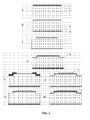
- Fig. 1 illustrates the process steps of fabrication of a germanium solar cell passivated by the method according to the present invention according to preferred embodiments described in detail in the specification.
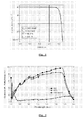
- Fig. 2 illustrates the performance of a solar cell according to a preferred embodiment.
- the short circuit current (J sc ) is equal to 40.4 mA/cm 2
- the open circuit voltage Voc is equal to 248 mV
- the fill factor (FF) is found to be 66.3%.
- An AM1.5 efficiency of 6.64 % is measured.
- Fig. 3 illustrates the internal quantum efficiency, the external quantum efficiency, and the reflectance of a solar cell created by a preferred embodiment of the present invention, in function of the wavelength of the incoming light.
- the good quality of the passivation layer is shown by the excellent response at low wavelengths.
- Fig. 4 shows simulation results where the emitter thickness and surface recombination velocities have been varied.
- Fig. 5 is the carrier lifetime is plotted in function of the duration of the exposure time of the substrate to the H 2 plasma during the preliminary cleaning step.
- Fig. 6 illustrates the process of achieving laser fired contacts (LFC), according to embodiments of the present invention.
- Fig. 7(a) through (c) provides SEM pictures of an Al-a-Si-Ge interface where a laser beam has been applied.
- the power was about 0.4W, whereas it was about 1W in Fig. 7(b) and 0.6W in Fig. 7(c).
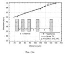
- Figs. 8(a) and 8(b) provide results of a transfer length method (TLM) measurement and I-V characteristics of a LFC substrate, respectively.
- TLM transfer length method
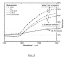
- Fig. 9 provides a measurement of the reflection of germanium substrates covered with different metals at the back.
- Fig. 10 is an overview of the several steps of a process for fabricating a germanium solar cell suited for application in a thermophotovoltaic device (so-called LFC cell).
- Fig. 11 is representing the IV-characteristics of the germanium LFC solar cell, measured using the AM1.5 spectrum.
- Fig. 12 is describing the quantum efficiency of a germanium photovoltaic cell using a LFC back contact.
- Fig. 13 is describing a normalized external quantum efficiency (EQE) and reflection of a laser fired cell (cell B) and a classical contacted germanium solar cell.
- Fig. 14 is representing the IV-characteristics of a diced germanium photovoltaic cell with a full aluminium rear contact, measured using the AM1.5 spectrum.
- a method for passivating and contacting a germanium substrate comprising a) providing a germanium substrate with a first surface; this germanium surface can be doped or undoped; b) depositing a layer of amorphous silicon on top of the germanium surface.
- PECVD plasma enhanced chemical vapor deposition
- the thickness of the layer is generally less than 500 nm. More preferably, the thickness of the layer is less than 300 nm. Even more preferably, the thickness of the layer is less than about 100 nm. Most preferably, for front surface applications, the thickness of the layer is less than about 40 nm.
- the thickness of the layer is from about 10 to about 40 nm, e.g., from about 15 nm, 20 nm, or 25 nm to about 30 nm, 35 nm, or 40 nm.
- the thickness can typically be larger, since the effect of absorption of incident light on the performance is minimal.
- the thickness is preferably from about 20 nm to about 100nm. More preferably the thickness is from about 40 nm to about 90 nm. Even more preferably the thickness is from about 50 nm to about 80 nm. If the thickness becomes too large, it may become more difficult to diffuse/fire the contact metal through the layer.
- the cleaning treatment preceding the deposition, gas flow composition and applied RF-power for forming the plasma is performed at a wafer temperature of from about 150°C to about 250°C or 300°C, e.g., from about 160°C, 170°C, 180°C, 190°C, 200°C, or 210°C to about 220°C, 230°C, 240°C, 250°C, 275°C, or 300°C.
- a higher deposition temperature results in out-diffusion of the hydrogen within the material, which subsequently results in less desirable passivation properties; c) depositing a patterned layer of metal on top of the layer of amorphous silicon.
- the metal is a highly conductive metal such as Pd, Cu, Ag, Au or Al.
- Pd, Cu, Ag, and Au are advantageously used in front surface applications, while Al can advantageously be used for backside passivation schemes.
- the aluminium can generate a back surface field (BSF), which would not be desirable on the front surface; if employed in front surface applications, Al could possibly form a p++ region which repels the holes at the front side, preventing collection of the holes on the front.
- BSF back surface field
- a multi-layer comprising two or more different metal layers can be applied, such as Pd/Ag, Pd/Au, or Pd/Cu. This step can comprise different sub steps.
- This layer can be patterned to form a contact grid; and d) "Firing through” or diffusion of the metal through the layer of amorphous silicon by applying a temperature step, such that the germanium surface is contacted.
- the diffusion step should be chosen such that the process can be controlled.
- the effect of the diffusion or fire through is that metal particles of the contact layer penetrate through the amorphous silicon passivation layer to form a conductive path between the contact and the Ge-substrate.
- the resulting contacting resistivity is preferably lower than 5.10 -4 ⁇ cm 2 , more preferably lower than 10 -4 ⁇ cm 2 , most preferably lower than 10 -5 ⁇ cm 2 .
- the quality of the passivation layer is strongly affected by the cleaning treatment preceding the deposition. For instance a wet-chemical HF-dip and a H 2 plasma can be used to prepare the surface.
- a method of passivating and contacting a surface of a germanium substrate including:
- the contact resistivity is preferably less than about 10 -4 ⁇ cm 2 .
- the method can further include cleaning the first surface before forming the passivation layer, the cleaning including applying wet-chemical HF treatment and a H 2 containing plasma to the first surface.
- Forming the passivation layer can be performed by plasma enhanced chemical vapor deposition (PECVD).
- PECVD plasma enhanced chemical vapor deposition
- the PECVD can be performed at a temperature of from about 150°C to about 300°C.
- the passivation layer can have a thickness of less than about 100 nm.
- the passivation layer can have a thickness of less than about 40 nm.
- the passivation layer can have a thickness of from about 10 nm to about 50 nm.
- the first surface can be a surface of a germanium solar cell, a thermo photovoltaic cell, or a photodetector.
- the contact layer includes Ag, Au, Pd, or Cu.
- the contact layer can also comprise a multi-layer, as for instance Pd/Ag, Pd/Au, or Pd/Cu multi-layers.
- the contact layer can be patterned to form a contact grid.
- the heating can be performed at a temperature lower than about 300°C.
- the heating can be performed at a temperature of from about 180°C to about 240°C.
- the method can further include (a) forming an emitter area in the germanium substrate; (b) forming a back contact on a second surface of the germanium substrate and thereby realizing a back surface field; (c) etching mesa structures so as to define photo voltaic cell regions; and (d) forming an antireflective coating on the exposed parts of the passivation layer and the contact layer.
- the forming of an emitter area, forming a back contact, and etching mesa structures can be performed before forming a passivation layer.
- Forming an antireflective coating can be performed after the heating step.
- a passivated germanium substrate including a germanium substrate including a first surface; a passivation layer of plasma enhanced chemical vapor deposition (PECVD) deposited amorphous silicon material formed on the first surface; and a metal contacting layer on the passivation layer contacting the substrate through the passivation layer, by particles of the metal having penetrated into the passivation layer and thereby having formed a conductive path between the contacting layer and the germanium substrate.
- PECVD plasma enhanced chemical vapor deposition
- the passivation layer preferably includes a conductive material in an area underlying the contacting layer and between the contacting layer and the germanium substrate.
- the passivation layer has a thickness of from about 10 to about 40 nm.
- a photovoltaic device including a germanium substrate including a first surface; a passivation layer of plasma enhanced chemical vapor deposition (PECVD) deposited amorphous silicon material formed on the first surface; and a contacting layer including a conductive material formed on the passivation layer.
- PECVD plasma enhanced chemical vapor deposition
- a method of passivating and contacting a surface of a germanium substrate comprising: providing a germanium substrate having a first surface; cleaning the first surface by applying a wet-chemical HF dip to the first surface and thereafter applying a H 2 containing plasma to the first surface; forming a passivation layer of amorphous silicon material on the first surface; forming a contact layer of metal on the passivation layer; and heating the substrate and the layers so that the first surface makes contact with the contact layer through the passivation layer.
- the method can further comprise forming an emitter area in the germanium substrate; forming a back contact on a second surface of the germanium substrate and thereby realizing a back surface field; etching mesa structures so as to define photo voltaic cell regions; and forming an antireflective coating on the exposed parts of the passivation layer and the contact layer.
- a method of passivating and contacting a surface of a germanium substrate comprising providing a germanium substrate having a first surface, wherein the first surface is configured to be used as a back surface of a photovoltaic device; forming a first passivation layer comprising an amorphous silicon material on the first surface; forming a contact layer on the first passivation layer, wherein the contact layer comprises a first metal layer, the first metal layer comprising aluminium; and heating the substrate and the layers so that the first surface makes contact with the contact layer through the first passivation layer.
- the first metal layer can comprise or consist essentially of aluminium.
- Heating the substrate and the layers can be performed locally, in a predetermined contact area.
- the heating can be performed by means of a laser.
- the contact layer can be a continuous layer configured for use as a mirroring surface for the back surface.
- the contact resistivity of a conductive path between the contact layer and the substrate is preferably less than about 10 -4 ⁇ cm 2 .
- the method can further comprise cleaning the first surface before forming the first passivation layer, the cleaning comprising applying a H 2 containing plasma to the first surface.
- the method can further comprise cleaning the first surface before forming the first passivation layer, the cleaning comprising applying a wet-chemical HF dip to the first surface.
- the first passivation layer can be performed by plasma enhanced chemical vapor deposition.
- the plasma enhanced chemical vapor deposition is preferably performed at a temperature of from about 150°C to about 300°C.
- the first passivation layer has preferably a thickness of less than about 100 nm.
- the first passivation layer can preferably have a thickness of less than about 80 nm.
- the first passivation layer can have a thickness of from about 20 nm to about 100 nm.
- a photovoltaic device can obtained by the methods described according to the present invention, wherein the photovoltaic device is selected from the group consisting of a solar cell, a thermo photovoltaic cell, and a photodetector.
- the contact layer can further comprise an additional metal layer, the additional metal layer comprising or consisting of at least one metal selected from the group consisting of Cu, Ag, and Au.
- the first metal layer can be deposited atop the first passivation layer, wherein the additional metal layer is deposited atop the first metal layer.
- the additional metal layer can be deposited by evaporation, or by electroplating.
- the contact layer can be patterned to form a contact grid.
- the heating is preferably performed at a temperature lower than about 300°C.
- the heating can be performed at a temperature of from about 180°C to about 240°C.
- the method can further comprise forming an emitter area in the germanium substrate; forming a second passivation layer comprising an amorphous silicon material on a second surface of the germanium substrate, wherein the second surface is configured for use as front surface of a photovoltaic device; forming a front contact layer on the second passivation layer, wherein the front contact layer comprises a second metal layer; and heating the substrate and the layers so that the second surface makes contact with the front contact layer through the second passivation layer.
- the second metal layer can comprise a metal selected from the group consisting of Pd, Cu, Ag, and Au. Only one heating step can be performed for the front surface and the back surface. The second surface can make contact with the front contact layer through the second passivation layer before the first surface makes contact with the contact layer through the first passivation layer.
- a passivated germanium substrate comprising a germanium substrate comprising a first surface; a passivation layer comprising an amorphous silicon material formed on the first surface; and a metal contacting layer on the passivation layer, the metal contacting layer contacting the substrate through the passivation layer, by particles of the metal that are penetrated into the passivation layer to form a conductive path between the contacting layer and the germanium substrate, wherein the contacting layer comprises a first metal layer, the first metal layer comprising aluminium.
- the amorphous silicon material can be deposited by for instance and preferably plasma enhanced chemical vapor deposition.
- the passivation layer preferably comprises a conductive material in an area underlying the contacting layer and between the contacting layer and the germanium substrate.
- the passivation layer has preferably a thickness of from about 20 nm to about 100 nm.
- a photovoltaic device comprising a germanium substrate having a first surface; a passivation layer comprising an amorphous silicon material formed on the first surface; and a contacting layer comprising a conductive material formed on the passivation layer, wherein the contacting layer comprises a first metal layer, the first metal layer comprising aluminium.
- the amorphous silicon material can be deposited by plasma enhanced chemical vapor deposition.
- a photovoltaic device comprising a germanium substrate having a first surface and a second surface; a first passivation layer comprising amorphous silicon material formed on the first surface; a second passivation layer comprising amorphous silicon material formed on the second surface; a first contacting layer comprising a conductive material formed on the first passivation layer, wherein the first contacting layer comprises aluminium; and a second contacting layer comprising a conductive material formed on the second passivation layer, wherein the second contacting layer comprises a metal selected from the group consisting of Pd, Cu, Ag, and Au.
- the amorphous silicon material can be deposited, for instance and preferably by plasma enhanced chemical vapor deposition.
- the photovoltaic device can preferably comprise a barrier layer in between the contact layer and in particular the back contact layer, made of aluminium and the passivation layer just underneath.
- Said barrier layer is accordingly a layer that is deposited between the amorphous silicon layer (passivation layer) and the aluminium layer (back contact layer).
- the preferred material for said barrier layer can be MgF 2 (through e-beam evaporation), ZnS (through e-beam evaporation),SiO x as eg SiO 2 (through PEC) and Si x N y , as eg Si 3 N 4 (through PEC.
- This barrier layer has two functions:
- a method for the production of a germanium solar cell is described in detail referring to the steps disclosed in Fig.1.
- SOD spin-on dopant (3)
- a possible alternative is the reversed situation with a p + emitter in the n-type substrate.
- the most relevant parameters are the diffusion time, diffusion temperature, diffusion atmosphere, and the phosphorous content of the SOD.
- the diffusion temperature is preferably from about 500 to about 700°C. More preferably a temperature of about 600 °C is used.
- the diffusion time is preferably from about 10 seconds to about 20 minutes. More preferably a diffusion time of about 30 seconds is used.
- the diffusion atmosphere is preferably a forming gas such as N 2 +H 2 (10%). Subsequent to the diffusion the spin-on material is removed using an HF solution.
- the Al is diffused into the substrate by applying a temperature step in a forming gas (preferably N 2 +H 2 (10%)) to create a p + zone that serves as a back surface field (BSF) (5).
- a forming gas preferably N 2 +H 2 (10%)
- Preferably an about 1 ⁇ m thick aluminium layer is evaporated.
- the diffusion temperature is preferably from about 350 to about 600°C.
- the diffusion time is preferably from about 10 minutes to about 60 minutes.
- the diffusion atmosphere is preferably a forming gas such as N 2 +H 2 (10%).
- the surface is prepared by a wet-chemical treatment using HF and subsequently applying a H 2 plasma, inside the deposition chamber, performed just before the deposition of the amorphous silicon.
- the applied RF power is less than 50 Watt. More preferably the power is less than 15 Watt.
- the exposure time is preferably less than 2 minutes; more preferably the exposure time can be chosen between 30 and 45 seconds.
- the thickness of the layer is less than about 100 nm. More preferably a thickness of smaller than about 50 nm or about 40 nm can be chosen.
- a thickness of about 10 nm to about 40 nm or 50 nm can be chosen, which can be especially advantageous when considering front side passivation schemes.
- the thickness is preferably greater, as described above. Thicker layers may absorb too much light, which can be disadvantageous when a high efficiency of a solar cell is important.
- Gas flow composition and applied RF-power are critical for forming the plasma.
- the PECVD is performed at a wafer temperature of from about 150 to about 250°C.
- the plasma is from about 6 to about 20 Watts.
- the gas composition comprises from about 20 to about 100 sccm SiH 4 and from about 0 to about 600 sccm H 2 .
- the metal preferably silver (Ag) copper (Cu) or gold (Au) contact structure (E), using preferably lift-off to define the finger pattern (F,7).
- the metal preferably silver (Ag) copper (Cu) or gold (Au) contact structure (E)
- a multi-layer of different types of metal can be used like Pd/Ag, Pd/Cu, or Pd/Au.
- the material of the first layer, preferably Pd is diffused through the passivation layer to obtain a low contact resistance.
- the second, preferably highly conductive metal layer such as Ag, Cu or Au, serves to obtain a low series resistance.
- the second layer can be evaporated or applied by electro-plating.
- a multi-layer comprising a 50 nm layer and a 2 ⁇ m layer can be applied.
- Cu as a second layer in the multilayer can be advantageous since it can be applied via electroplating and thus allow formation of thick layers (e.g., thicker then 2 microns), which can be desirable in applications where high currents are generated, as in, for instance, thermophotovoltaic systems or concentrator systems.
- the diffusion temperature is preferably from about 150 to about 300°C, for instance, about 220°C. More preferably a temperature of from about 160 or 170 °C to about 250 °C is used, and most preferably, a temperature of from about 180 °C to about 230 °C or 240 °C is used.
- the diffusion time is preferably between 1 min and 60 min. Depending on the thickness of the passivation layer, the optimal diffusion time will change.
- the diffusion atmosphere is preferably a forming gas (as N2 + H2 (10%)).
- a method for the production of a germanium solar cell is described referring to the same steps represented in Fig. 1:
- a diffusion temperature of 600 °C and a diffusion time of 30 seconds were used.
- the diffusion atmosphere was a forming gas, N 2 +H 2 (10%).
- the lift off comprised selectively depositing a resist layer on the layer of amorphous silicon before the Pd/Ag deposition. After the following Pd/Ag deposition the resist is removed - together with the Pd/Ag deposited on the resist, such that only the area where no resist had been applied remains covered with Ag. A 50 nm palladium and a 2 ⁇ m thick silver layer were used.
- Firing through the amorphous silicon layer of the applied Pd/Ag contacts (diffusion of palladium through the passivating amorphous silicon layer) in order to obtain a good contact with the n + germanium emitter.
- Critical are the diffusion time and temperature. A diffusion temperature of 220 °C and a diffusion time of about 2 to 20 minutes were used. The diffusion atmosphere was a forming gas (N2 + H2 (10%)).
- Fig. 2 illustrates the performance of a solar cell according to a preferred embodiment of the present invention.
- the short circuit current (J sc ) is equal to 40.4 mA/cm 2
- the open circuit voltage Voc is equal to 248 mV
- the fill factor (FF) was found to be 66.3%.
- An AM1.5 efficiency of 6.64 % was measured.
- Fig. 3 illustrates the internal quantum efficiency, the external quantum efficiency, and the reflectance of a solar cell created by a preferred embodiment of the present invention, in function of the wavelength of the incoming light.
- Fig. 4 shows simulation results where the emitter thickness and surface recombination velocities have been varied.
- Cell 1 has a simulated front surface recombination velocity (S front ) of 70000 cm/s and cell 2 has S front equal to 50 cm/s. With decreasing emitter depth and decreasing recombination velocity at the front surface the response of the cell improves.
- a 1 ⁇ m thick metal contact layer can be deposited by evaporation. Subsequently, the metal can be heated locally by applying a laser pulse.
- a laser pulse For this application, a green (532nm) YAG laser can be employed; however, other lasers can also be employed. The heating generated by the laser pulse results in the diffusion of the metal through the amorphous silicon and inside the germanium layer forming the contact. Aluminium is advantageous for back surface contacting, because aluminium dopes the germanium and thereby forms a local p + layer at the contact that acts as a back surface field. Aluminium also exhibits good reflective properties.
- the power of the laser is chosen such that it can be used in the processes as described above. Therefore several parameters can be adjusted as desired. Some parameters that can be adjusted include the current through the laser diode, the moving speed of the laser head, and the focusing of the laser beam.
- the contact resistance was measured for the contact shown in Figure 7(c) using the transfer length method. In this measurement, the resistance between two contact points was measured over several increasing distances and the results are shown in Figures 8(a) and 8(b). The resistance showed an Ohmic character. Based on the results of the measurement of the contact shown in Figure 7(c), a specific contact resistance of about 7.6.10 -4 ⁇ -cm is calculated, which makes this technique suitable for TPV applications.
- a first-time germanium TPV cell has been developed using LFC. It is believed that the laser lines as a contact grid at the back can be further optimized, improving the device, for example, by improving the Fill Factor (FF). Solar cell behavior has also been observed.
- FF Fill Factor
- the methods for passivating and contacting according to the preferred embodiments can be applied to the front surface as well as to the back surface of the photovoltaic device, thus also to both surfaces. This results in corresponding devices.
- a single firing step can be performed for firing front as well as back contacts.
- the amorphous layer can in certain embodiments be applied to both sides at the same time, in a single step. This can be done by a proper design of the deposition chamber and/or choosing certain orientations of the Ge wafers. In a typical chamber the wafers can be placed at an angle with respect to the horizontal direction (defined as orthogonal to the direction of gravity), as, for example, vertical ( i.e ., an angle of 90 degrees).
- the firing step can be performed locally (e.g ., defining a pattern), for example, by use of a laser.
- a laser allows for local heating.
- the methods of these embodiments are particularly desirable in the case of back surface applications, where patterning of the metal layer is not necessary.
- a eutectic alloy e.g. , GeAl on the back surface
- a continuous layer which serves as a reflector, also called mirror surface.
- a local heating by, for example, a laser can provide a good contact pattern, and leaves the remaining Ge/Al interface as is, such that its reflecting properties are not jeopardized.
- Fig. 9 shows some measurements which illustrate the reflection properties, measured from the font, of a 90 ⁇ m germanium substrate covered on the backside with, respectively, gold, silver, amorphous silicon-gold, amorphous silicon-silver and an annealed (440°C, 20 min) aluminium layer.
- the front side of the substrate was covered with a ZnS/MgF 2 anti-reflective (AR) coating.
- the annealed aluminium layer at the back gives a relatively low reflection of a maximum of 20 percent at 1800 nm.
- Using a good reflective metal like gold or silver increases the reflectivity up to 50 percent at 1800 nm. The fact that the effect of the backside reflection only takes place for high wavelengths can be explained by only these photons reaching the backside of the cell.
- back surface passivation is desirable. This can be achieved by applying, e.g., a thin (50 nm) layer of amorphous silicon by PECVD. This passivation layer is located between the germanium substrate and the metal layer at the back, and lowers the reflectance by 10% when compared to the metal layer only, but the reflectance is still twice as good when compared to the annealed aluminium contact.
- the metal can be patterned and fired by an overall heating step, or by an overall illumination by a laser of the appropriate energy, and on the backside a continuous layer can be applied locally contacting the Ge substrate, by a laser treatment along a predetermined contact pattern.
- Different metals can be used on the front and back surfaces.
- the back side metal can be patterned and fired by local or general heating, after which an additional mirror layer can be provided in the areas where no back contact is provided. This may require additional patterning or masking.
- the additional mirror layer is preferably selected such that it does not easily diffuse through the passivation layer and/or into the germanium substrate upon contact firing. It is preferably selected such that the reflectivity of the interface between the additional mirror layer and the passivation layer / germanium substrate is left substantially intact during contact firing.
- Fig. 5 the measured effective minority carrier lifetime is plotted in function of the duration of the exposure time of the substrate to the H2 plasma during the preliminary cleaning step.
- the amount of exposure plays a significant role in the optimization of the solar cell efficiency.
- a further improvement of the quality of the passivation can be achieved by optimizing the layer thickness.
- a layer that is too thin results in lower quality passivation properties, while a layer that is too thick absorbs a larger part of the solar spectrum.
- the restrictions concerning the thickness are less stringent since in these applications the part of the spectrum that is used by the germanium cell will not be absorbed in the amorphous silicon layer.
- a further improvement of the method according to the invention relates to the use of Ag for the back contacts.
- a barrier layer present in between the passivation layer and the contact will be formed.
- the cell (so called LFC cell) process that has been developed consists in seven basic steps. A schematic overview of these steps is shown in Fig. 10.
- n + emitter realized by diffusion of phosphorous from a spin-on dopant which is applied by spin coating, see Fig. 10(a).
- the diffusion profile is optimized by changing the phosphorous concentration in the spin-on dopant, the spin speed and the diffusion temperature and time.
- a crucial step for obtaining high cell efficiencies is the passivation of the front and back surface, Fig. 10 (b).
- a thin layer of amorphous silicon is deposited by application of Plasma Enhanced Chemical Vapour Deposition (PECVD). The surface pre-treatment and plasma conditions are of crucial importance for the quality of amorphous silicon passivation.
- PECVD Plasma Enhanced Chemical Vapour Deposition
- a palladium (Pd)/silver (Ag) stack is used as a front contact, see Fig. 10(c), where Pd will diffuse through the amorphous silicon layer.
- the additional layer of silver is used to realize a low series resistance contact.
- a dual layer of zinc-sulfide (ZnS) and aluminium will be applied, see Fig. 10(d).
- the ZnS layer acts like a diffusion barrier during the subsequent annealing step such that diffusion of aluminium through the amorphous silicon is prevented when annealing the front contact.
- the back surface reflection can be optimized.
- contact at the backside will be realized by local heating with a laser (Fig. 10(e)).
- the aluminum layer is locally heated and contact is being made through the ZnS and a-Si layer.
- annealing is done to diffuse the palladium through the amorphous silicon layer and to anneal the laser fired contact (Fig.10(f)). Optimization of the annealing time is crucial since a too short time does not leave a contact and a too long time results in a shorted cell.
- a dual layer antireflective coating consisting of ZnS and MgF 2 is deposited to increase light transmission into the germanium (Fig.10(g)).
- thermophotovoltaic cell has been realized with an efficiency of 6.3% and an V oc of 243.1 mV, a J sc of 44.5 mA/cm -2 and a FF of 58.5% as shown in Figure 11.
- Figures 12 and 13 show the quantum efficiency curves of the LFC contacted cell demonstrating the improved response of this cell in high wavelength regions.
- the most important motivation for using laser fired contacts in germanium TPV cells is the higher reflectance and thus higher spectral response for incoming photons with high wavelengths.
- our "standard" germanium solar cells an aluminium diffused back contact is used.
- Figure 13 the reflectance and normalized EQE which has been measured on the two different types of germanium solar cells has been compared. Each cell has the same emitter and front contact grid, but one cell has a diffused aluminium rear contact and the other a LFC contact.
- a 0.5 ⁇ 0.5 cm 2 cell has been realized with a record efficiency of 8.4 percent, with a J sc of 50 mA/cm 2 , a V oc of 258 mV and a FF of 65 percent.
- This cell has been separated from other cells by dicing using a diamond wafer dicer.
- the IV-curve of this cell is shown in Figure 14.
Landscapes
- Engineering & Computer Science (AREA)
- Computer Hardware Design (AREA)
- Microelectronics & Electronic Packaging (AREA)
- Power Engineering (AREA)
- Physics & Mathematics (AREA)
- Condensed Matter Physics & Semiconductors (AREA)
- Electromagnetism (AREA)
- General Physics & Mathematics (AREA)
- Life Sciences & Earth Sciences (AREA)
- Sustainable Development (AREA)
- Sustainable Energy (AREA)
- Chemical & Material Sciences (AREA)
- Manufacturing & Machinery (AREA)
- Inorganic Chemistry (AREA)
- Crystallography & Structural Chemistry (AREA)
- Photovoltaic Devices (AREA)
Applications Claiming Priority (2)
| Application Number | Priority Date | Filing Date | Title |
|---|---|---|---|
| US11/246,509 US7960645B2 (en) | 2003-05-07 | 2005-10-07 | Germanium solar cell and method for the production thereof |
| US11/340,171 US8664525B2 (en) | 2003-05-07 | 2006-01-26 | Germanium solar cell and method for the production thereof |
Publications (2)
| Publication Number | Publication Date |
|---|---|
| EP1772907A2 true EP1772907A2 (de) | 2007-04-11 |
| EP1772907A3 EP1772907A3 (de) | 2014-12-10 |
Family
ID=37670953
Family Applications (1)
| Application Number | Title | Priority Date | Filing Date |
|---|---|---|---|
| EP06121983.8A Withdrawn EP1772907A3 (de) | 2005-10-07 | 2006-10-09 | Germanium-Solarzelle und Verfahren zu ihrer Herstellung |
Country Status (2)
| Country | Link |
|---|---|
| US (1) | US8664525B2 (de) |
| EP (1) | EP1772907A3 (de) |
Cited By (3)
| Publication number | Priority date | Publication date | Assignee | Title |
|---|---|---|---|---|
| DE102008046480A1 (de) * | 2008-09-09 | 2010-03-11 | Solarworld Innovations Gmbh | Verfahren zur Herstellung einer lötbaren LFC-Solarzellenrückseite und aus derartigen LFC-Solarzellen verschaltetes Solarmodul |
| DE102008049220A1 (de) * | 2008-09-27 | 2010-06-24 | Solarworld Innovations Gmbh | Halbleiterbauelement mit Kontakten aus einlegierten Metalldrähten |
| EP2936561A4 (de) * | 2012-12-21 | 2015-12-23 | Sunpower Corp | Verbesserte haftung einer keimschicht für leitfähigen kontakt einer solarzelle |
Families Citing this family (19)
| Publication number | Priority date | Publication date | Assignee | Title |
|---|---|---|---|---|
| US20100012175A1 (en) * | 2008-07-16 | 2010-01-21 | Emcore Solar Power, Inc. | Ohmic n-contact formed at low temperature in inverted metamorphic multijunction solar cells |
| US9287438B1 (en) * | 2008-07-16 | 2016-03-15 | Solaero Technologies Corp. | Method for forming ohmic N-contacts at low temperature in inverted metamorphic multijunction solar cells with contaminant isolation |
| US20120104460A1 (en) | 2010-11-03 | 2012-05-03 | Alta Devices, Inc. | Optoelectronic devices including heterojunction |
| US8686284B2 (en) * | 2008-10-23 | 2014-04-01 | Alta Devices, Inc. | Photovoltaic device with increased light trapping |
| TW201030998A (en) * | 2008-10-23 | 2010-08-16 | Alta Devices Inc | Photovoltaic device |
| CN102257635A (zh) * | 2008-10-23 | 2011-11-23 | 奥塔装置公司 | 光伏器件的薄吸收层 |
| MY186820A (en) * | 2009-04-21 | 2021-08-23 | Tetrasun Inc | High-efficiency solar cell structures and methods of manufacture |
| US9691921B2 (en) | 2009-10-14 | 2017-06-27 | Alta Devices, Inc. | Textured metallic back reflector |
| US20170141256A1 (en) | 2009-10-23 | 2017-05-18 | Alta Devices, Inc. | Multi-junction optoelectronic device with group iv semiconductor as a bottom junction |
| US9502594B2 (en) | 2012-01-19 | 2016-11-22 | Alta Devices, Inc. | Thin-film semiconductor optoelectronic device with textured front and/or back surface prepared from template layer and etching |
| US9768329B1 (en) | 2009-10-23 | 2017-09-19 | Alta Devices, Inc. | Multi-junction optoelectronic device |
| US11271128B2 (en) | 2009-10-23 | 2022-03-08 | Utica Leaseco, Llc | Multi-junction optoelectronic device |
| US20150380576A1 (en) | 2010-10-13 | 2015-12-31 | Alta Devices, Inc. | Optoelectronic device with dielectric layer and method of manufacture |
| CN102148288A (zh) * | 2011-01-27 | 2011-08-10 | 东方电气集团(宜兴)迈吉太阳能科技有限公司 | 采用激光快速加热法制备单晶硅太阳能电池片背面钝化层的工艺 |
| US10011920B2 (en) | 2011-02-23 | 2018-07-03 | International Business Machines Corporation | Low-temperature selective epitaxial growth of silicon for device integration |
| US11038080B2 (en) | 2012-01-19 | 2021-06-15 | Utica Leaseco, Llc | Thin-film semiconductor optoelectronic device with textured front and/or back surface prepared from etching |
| US9059212B2 (en) | 2012-10-31 | 2015-06-16 | International Business Machines Corporation | Back-end transistors with highly doped low-temperature contacts |
| US8912071B2 (en) * | 2012-12-06 | 2014-12-16 | International Business Machines Corporation | Selective emitter photovoltaic device |
| US10283665B2 (en) * | 2013-07-08 | 2019-05-07 | Sifotonics Technologies Co., Ltd. | Compensated photonic device structure and fabrication method thereof |
Citations (4)
| Publication number | Priority date | Publication date | Assignee | Title |
|---|---|---|---|---|
| US4589006A (en) * | 1982-08-23 | 1986-05-13 | The United States Of America As Represented By The United States Department Of Energy | Germanium detector passivated with hydrogenated amorphous germanium |
| JPH104204A (ja) * | 1996-06-18 | 1998-01-06 | Sharp Corp | 太陽電池の製造方法 |
| US6210991B1 (en) * | 1997-04-23 | 2001-04-03 | Unisearch Limited | Metal contact scheme using selective silicon growth |
| EP1475844A2 (de) * | 2003-05-07 | 2004-11-10 | Interuniversitair Microelektronica Centrum Vzw | Germanium-Solarzelle und deren Herstellungsverfahren |
Family Cites Families (20)
| Publication number | Priority date | Publication date | Assignee | Title |
|---|---|---|---|---|
| GB1355890A (en) | 1972-04-29 | 1974-06-05 | Ferranti Ltd | Contacts for solar cells |
| US4473597A (en) * | 1978-02-01 | 1984-09-25 | Rca Corporation | Method and structure for passivating a PN junction |
| US4319395A (en) * | 1979-06-28 | 1982-03-16 | Motorola, Inc. | Method of making self-aligned device |
| JPS56155526A (en) * | 1980-05-06 | 1981-12-01 | Shunpei Yamazaki | Method of forming film |
| JPS58197717A (ja) * | 1982-05-13 | 1983-11-17 | Toshiba Corp | 半導体装置の製造方法 |
| US4724011A (en) * | 1983-05-16 | 1988-02-09 | Atlantic Richfield Company | Solar cell interconnection by discrete conductive regions |
| JPS61294460A (ja) * | 1985-06-21 | 1986-12-25 | Tohoku Ricoh Co Ltd | 電子写真感光体 |
| US4776894A (en) * | 1986-08-18 | 1988-10-11 | Sanyo Electric Co., Ltd. | Photovoltaic device |
| US5083007A (en) * | 1990-08-01 | 1992-01-21 | Microelectronics And Computer Technology Corporation | Bonding metal electrical members with a frequency doubled pulsed laser beam |
| JPH0548127A (ja) * | 1991-08-19 | 1993-02-26 | Showa Shell Sekiyu Kk | 非晶質シリコン太陽電池及びその製造方法 |
| US5437736A (en) * | 1994-02-15 | 1995-08-01 | Cole; Eric D. | Semiconductor fiber solar cells and modules |
| US6165876A (en) * | 1995-01-30 | 2000-12-26 | Yamazaki; Shunpei | Method of doping crystalline silicon film |
| DE19522539C2 (de) * | 1995-06-21 | 1997-06-12 | Fraunhofer Ges Forschung | Solarzelle mit einem, eine Oberflächentextur aufweisenden Emitter sowie Verfahren zur Herstellung derselben |
| US6339013B1 (en) * | 1997-05-13 | 2002-01-15 | The Board Of Trustees Of The University Of Arkansas | Method of doping silicon, metal doped silicon, method of making solar cells, and solar cells |
| US6103970A (en) * | 1998-08-20 | 2000-08-15 | Tecstar Power Systems, Inc. | Solar cell having a front-mounted bypass diode |
| US6632730B1 (en) * | 1999-11-23 | 2003-10-14 | Ebara Solar, Inc. | Method for self-doping contacts to a semiconductor |
| JP3586197B2 (ja) * | 2000-03-23 | 2004-11-10 | シャープ株式会社 | 薄膜形成用プラズマ成膜装置 |
| DE10046170A1 (de) * | 2000-09-19 | 2002-04-04 | Fraunhofer Ges Forschung | Verfahren zur Herstellung eines Halbleiter-Metallkontaktes durch eine dielektrische Schicht |
| US6645831B1 (en) * | 2002-05-07 | 2003-11-11 | Intel Corporation | Thermally stable crystalline defect-free germanium bonded to silicon and silicon dioxide |
| US7960645B2 (en) * | 2003-05-07 | 2011-06-14 | Imec | Germanium solar cell and method for the production thereof |
-
2006
- 2006-01-26 US US11/340,171 patent/US8664525B2/en active Active
- 2006-10-09 EP EP06121983.8A patent/EP1772907A3/de not_active Withdrawn
Patent Citations (4)
| Publication number | Priority date | Publication date | Assignee | Title |
|---|---|---|---|---|
| US4589006A (en) * | 1982-08-23 | 1986-05-13 | The United States Of America As Represented By The United States Department Of Energy | Germanium detector passivated with hydrogenated amorphous germanium |
| JPH104204A (ja) * | 1996-06-18 | 1998-01-06 | Sharp Corp | 太陽電池の製造方法 |
| US6210991B1 (en) * | 1997-04-23 | 2001-04-03 | Unisearch Limited | Metal contact scheme using selective silicon growth |
| EP1475844A2 (de) * | 2003-05-07 | 2004-11-10 | Interuniversitair Microelektronica Centrum Vzw | Germanium-Solarzelle und deren Herstellungsverfahren |
Non-Patent Citations (4)
| Title |
|---|
| HANSEN W L ET AL: "PROTECTIVE SURFACE COATINGS ON SEMICONDUCTOR NUCLEAR RADIATION DETECTORS", IEEE TRANS. ON NUCLEAR SCIENCE,, vol. 27, no. 1, 1 February 1980 (1980-02-01), pages 247-251, XP001432804, * |
| JACK T WALTON ED - JACK T WALTON: "SILICON DETECTORS: NEW CHALLENGES", NUCLEAR INSTRUMENTS AND METHODS IN PHYSICS RESEARCH, vol. 226, no. 1, 1 September 1984 (1984-09-01), XP001432223, * |
| LUKE P N ET AL: "Amorphous Ge bipolar blocking contacts on Ge detectors", PROCEEDINGS OF THE NUCLEAR SCIENCE SYMPOSIUM AND MEDICAL IMAGING CONFERENCE. SANTA FE, NOV. 2 - 9, 1991; [PROCEEDINGS OF THE NUCLEAR SCIENCE SYMPOSIUM AND MEDICAL IMAGING CONFERENCE], NEW YORK, IEEE, US, vol. -, 2 November 1991 (1991-11-02), pages 85-89, XP010057968, DOI: 10.1109/NSSMIC.1991.258915 ISBN: 978-0-7803-0513-7 * |
| WALTON J T ET AL: "Si(Li) x-ray detectors with amorphous Silicon passivation", IEEE NUCLEAR SCIENCE SYMPOSIUM. CONFERENCE RECORD, XX, XX, vol. 31, no. 1, 1 February 1984 (1984-02-01), pages 331-335, XP008082836, * |
Cited By (6)
| Publication number | Priority date | Publication date | Assignee | Title |
|---|---|---|---|---|
| DE102008046480A1 (de) * | 2008-09-09 | 2010-03-11 | Solarworld Innovations Gmbh | Verfahren zur Herstellung einer lötbaren LFC-Solarzellenrückseite und aus derartigen LFC-Solarzellen verschaltetes Solarmodul |
| DE102008046480A8 (de) * | 2008-09-09 | 2010-08-05 | Solarworld Innovations Gmbh | Verfahren zur Herstellung einer lötbaren LFC-Solarzellenrückseite und aus derartigen LFC-Solarzellen verschaltetes Solarmodul |
| DE102008049220A1 (de) * | 2008-09-27 | 2010-06-24 | Solarworld Innovations Gmbh | Halbleiterbauelement mit Kontakten aus einlegierten Metalldrähten |
| US8368163B2 (en) | 2008-09-27 | 2013-02-05 | Solarworld Innovations Gmbh | Semiconductor component with contacts made of alloyed-in metal wires |
| DE102008049220B4 (de) * | 2008-09-27 | 2015-11-19 | Solarworld Innovations Gmbh | Halbleiterbauelement mit Kontakten aus einlegierten Metalldrähten |
| EP2936561A4 (de) * | 2012-12-21 | 2015-12-23 | Sunpower Corp | Verbesserte haftung einer keimschicht für leitfähigen kontakt einer solarzelle |
Also Published As
| Publication number | Publication date |
|---|---|
| US8664525B2 (en) | 2014-03-04 |
| US20060207651A1 (en) | 2006-09-21 |
| EP1772907A3 (de) | 2014-12-10 |
Similar Documents
| Publication | Publication Date | Title |
|---|---|---|
| EP1772907A2 (de) | Germanium-Solarzelle und Verfahren zu ihrer Herstellung | |
| US9236510B2 (en) | Patterning of silicon oxide layers using pulsed laser ablation | |
| US7964789B2 (en) | Germanium solar cell and method for the production thereof | |
| US9455362B2 (en) | Laser irradiation aluminum doping for monocrystalline silicon substrates | |
| US8889462B2 (en) | Photovoltaic solar cells | |
| JP6046661B2 (ja) | 太陽電池、その製造方法及び太陽電池の不純物部形成方法 | |
| EP2149155B9 (de) | Herstellung eines hochwertigen rückseitigen kontakts mit lokaler rückseitiger siebdruckfläche | |
| Röder et al. | Add‐on laser tailored selective emitter solar cells | |
| US20130130430A1 (en) | Spatially selective laser annealing applications in high-efficiency solar cells | |
| US20120225515A1 (en) | Laser doping techniques for high-efficiency crystalline semiconductor solar cells | |
| US20110114171A1 (en) | Solar cell including sputtered reflective layer | |
| EP4350783A2 (de) | Hocheffiziente solarzellenstrukturen und herstellungsverfahren dafür | |
| US20130164883A1 (en) | Laser annealing applications in high-efficiency solar cells | |
| KR20070107660A (ko) | 백 콘택 태양 전지를 통한 이미터 랩 프로세스 및 제조방법 | |
| EP2472592B1 (de) | Solarzelle und Verfahren zu deren Herstellung | |
| EP2659518A2 (de) | Laserbearbeitungsverfahren für fotovotaische solarzellen | |
| US20170005206A1 (en) | Patterning of silicon oxide layers using pulsed laser ablation | |
| KR101878397B1 (ko) | 태양전지 및 그 제조 방법 | |
| US20140096820A1 (en) | Laser Doping of Crystalline Semiconductors Using a Dopant-Containing Amorphous Silicon Stack For Dopant Source and Passivation | |
| KR101954436B1 (ko) | 금속 실리사이드 층을 형성하는 방법 | |
| EP2819181A1 (de) | Laserglühanwendungen in hocheffizienten Solarzellen | |
| US7960645B2 (en) | Germanium solar cell and method for the production thereof | |
| WO2012162276A2 (en) | Spatially selective laser annealing applications in high-efficiency solar cells | |
| EP2645427A1 (de) | Erweiterte Laserablation bei der Solarzellenherstellung | |
| KR101406955B1 (ko) | 태양전지 및 그 제조방법 |
Legal Events
| Date | Code | Title | Description |
|---|---|---|---|
| PUAI | Public reference made under article 153(3) epc to a published international application that has entered the european phase |
Free format text: ORIGINAL CODE: 0009012 |
|
| AK | Designated contracting states |
Kind code of ref document: A2 Designated state(s): AT BE BG CH CY CZ DE DK EE ES FI FR GB GR HU IE IS IT LI LT LU LV MC NL PL PT RO SE SI SK TR |
|
| AX | Request for extension of the european patent |
Extension state: AL BA HR MK YU |
|
| RAP1 | Party data changed (applicant data changed or rights of an application transferred) |
Owner name: UMICORE N.V. Owner name: IMEC |
|
| PUAL | Search report despatched |
Free format text: ORIGINAL CODE: 0009013 |
|
| AK | Designated contracting states |
Kind code of ref document: A3 Designated state(s): AT BE BG CH CY CZ DE DK EE ES FI FR GB GR HU IE IS IT LI LT LU LV MC NL PL PT RO SE SI SK TR |
|
| AX | Request for extension of the european patent |
Extension state: AL BA HR MK RS |
|
| RIC1 | Information provided on ipc code assigned before grant |
Ipc: H01L 31/068 20120101ALI20141105BHEP Ipc: H01L 31/0216 20140101ALI20141105BHEP Ipc: H01L 31/052 20140101ALI20141105BHEP Ipc: H01L 31/028 20060101ALI20141105BHEP Ipc: H01L 31/18 20060101ALI20141105BHEP Ipc: H01L 31/0224 20060101AFI20141105BHEP |
|
| STAA | Information on the status of an ep patent application or granted ep patent |
Free format text: STATUS: THE APPLICATION HAS BEEN WITHDRAWN |
|
| 17P | Request for examination filed |
Effective date: 20150610 |
|
| RAX | Requested extension states of the european patent have changed |
Extension state: RS Payment date: 20150610 Extension state: HR Payment date: 20150610 Extension state: AL Payment date: 20150610 Extension state: BA Payment date: 20150610 Extension state: MK Payment date: 20150610 |
|
| RBV | Designated contracting states (corrected) |
Designated state(s): AT BE BG CH CY CZ DE DK EE ES FI FR GB GR HU IE IS IT LI LT LU LV MC NL PL PT RO SE SI SK TR |
|
| 18W | Application withdrawn |
Effective date: 20150619 |