EP1772776A1 - Method of patterning a positive tone resist layer overlaying a lithographic substrate and a computer program - Google Patents
Method of patterning a positive tone resist layer overlaying a lithographic substrate and a computer program Download PDFInfo
- Publication number
- EP1772776A1 EP1772776A1 EP06255143A EP06255143A EP1772776A1 EP 1772776 A1 EP1772776 A1 EP 1772776A1 EP 06255143 A EP06255143 A EP 06255143A EP 06255143 A EP06255143 A EP 06255143A EP 1772776 A1 EP1772776 A1 EP 1772776A1
- Authority
- EP
- European Patent Office
- Prior art keywords
- target
- pattern
- feature
- resist layer
- resist
- Prior art date
- Legal status (The legal status is an assumption and is not a legal conclusion. Google has not performed a legal analysis and makes no representation as to the accuracy of the status listed.)
- Withdrawn
Links
Images



Classifications
-
- G—PHYSICS
- G03—PHOTOGRAPHY; CINEMATOGRAPHY; ANALOGOUS TECHNIQUES USING WAVES OTHER THAN OPTICAL WAVES; ELECTROGRAPHY; HOLOGRAPHY
- G03F—PHOTOMECHANICAL PRODUCTION OF TEXTURED OR PATTERNED SURFACES, e.g. FOR PRINTING, FOR PROCESSING OF SEMICONDUCTOR DEVICES; MATERIALS THEREFOR; ORIGINALS THEREFOR; APPARATUS SPECIALLY ADAPTED THEREFOR
- G03F7/00—Photomechanical, e.g. photolithographic, production of textured or patterned surfaces, e.g. printing surfaces; Materials therefor, e.g. comprising photoresists; Apparatus specially adapted therefor
- G03F7/70—Microphotolithographic exposure; Apparatus therefor
- G03F7/70425—Imaging strategies, e.g. for increasing throughput or resolution, printing product fields larger than the image field or compensating lithography- or non-lithography errors, e.g. proximity correction, mix-and-match, stitching or double patterning
- G03F7/70466—Multiple exposures, e.g. combination of fine and coarse exposures, double patterning or multiple exposures for printing a single feature
-
- G—PHYSICS
- G03—PHOTOGRAPHY; CINEMATOGRAPHY; ANALOGOUS TECHNIQUES USING WAVES OTHER THAN OPTICAL WAVES; ELECTROGRAPHY; HOLOGRAPHY
- G03F—PHOTOMECHANICAL PRODUCTION OF TEXTURED OR PATTERNED SURFACES, e.g. FOR PRINTING, FOR PROCESSING OF SEMICONDUCTOR DEVICES; MATERIALS THEREFOR; ORIGINALS THEREFOR; APPARATUS SPECIALLY ADAPTED THEREFOR
- G03F1/00—Originals for photomechanical production of textured or patterned surfaces, e.g., masks, photo-masks, reticles; Mask blanks or pellicles therefor; Containers specially adapted therefor; Preparation thereof
- G03F1/36—Masks having proximity correction features; Preparation thereof, e.g. optical proximity correction [OPC] design processes
-
- G—PHYSICS
- G03—PHOTOGRAPHY; CINEMATOGRAPHY; ANALOGOUS TECHNIQUES USING WAVES OTHER THAN OPTICAL WAVES; ELECTROGRAPHY; HOLOGRAPHY
- G03F—PHOTOMECHANICAL PRODUCTION OF TEXTURED OR PATTERNED SURFACES, e.g. FOR PRINTING, FOR PROCESSING OF SEMICONDUCTOR DEVICES; MATERIALS THEREFOR; ORIGINALS THEREFOR; APPARATUS SPECIALLY ADAPTED THEREFOR
- G03F1/00—Originals for photomechanical production of textured or patterned surfaces, e.g., masks, photo-masks, reticles; Mask blanks or pellicles therefor; Containers specially adapted therefor; Preparation thereof
- G03F1/68—Preparation processes not covered by groups G03F1/20 - G03F1/50
- G03F1/70—Adapting basic layout or design of masks to lithographic process requirements, e.g., second iteration correction of mask patterns for imaging
-
- G—PHYSICS
- G03—PHOTOGRAPHY; CINEMATOGRAPHY; ANALOGOUS TECHNIQUES USING WAVES OTHER THAN OPTICAL WAVES; ELECTROGRAPHY; HOLOGRAPHY
- G03F—PHOTOMECHANICAL PRODUCTION OF TEXTURED OR PATTERNED SURFACES, e.g. FOR PRINTING, FOR PROCESSING OF SEMICONDUCTOR DEVICES; MATERIALS THEREFOR; ORIGINALS THEREFOR; APPARATUS SPECIALLY ADAPTED THEREFOR
- G03F7/00—Photomechanical, e.g. photolithographic, production of textured or patterned surfaces, e.g. printing surfaces; Materials therefor, e.g. comprising photoresists; Apparatus specially adapted therefor
- G03F7/70—Microphotolithographic exposure; Apparatus therefor
- G03F7/70425—Imaging strategies, e.g. for increasing throughput or resolution, printing product fields larger than the image field or compensating lithography- or non-lithography errors, e.g. proximity correction, mix-and-match, stitching or double patterning
- G03F7/70433—Layout for increasing efficiency or for compensating imaging errors, e.g. layout of exposure fields for reducing focus errors; Use of mask features for increasing efficiency or for compensating imaging errors
Definitions
- the present invention generally relates to photolithography and associated methods for exposing semiconductor substrates.
- Lithographic exposure apparatuses can be used, for example, in the manufacture of integrated circuits (ICs).
- a patterning device e.g. a mask or reticle provided with a mask pattern
- a beam of radiation is patterned by having that beam traverse the reticle, and is projected by a projection system of the lithographic apparatus onto a target portion (e.g., comprising one or more dies) on a substrate (silicon wafer) that has been coated with a layer of photo-active resist (i.e., photoresist) material, such as to image a desired pattern in the resist.
- a single wafer will contain a whole network of adjacent target portions that are successively irradiated via the projection system, one at a time.
- the smallest size of a repeatable feature (e.g., "half-pitch") of a pattern exposed on the wafer substrate that can be optically resolved by lithographic exposure apparatus depends on attributes of the projection system and the (patterned) projection beam of radiation.
- p 0.5 represents the repeatable feature size (e.g., "half-pitch") in nm;
- NA represents the numerical aperture of projection system
- ⁇ represents the wavelength of projection beam, in nm
- k 1 is a factor representative for the achievable optical resolution limit for the half-pitch feature size.
- the theoretical optical resolution half-pitch lower limit for k 1 is 0.25.
- considerable efforts have been directed to develop expensive technologies that are capable of employing shorter wavelengths and/or higher numerical apertures, thus allowing production of smaller features approaching the k 1 ⁇ 0.25 constraint.
- Fabrication of an integrated circuit pattern involves the control of space tolerances between features, as well as control of feature dimension tolerances.
- control of tolerances of the smallest dimensions such as for example the sizes of contacts or the width of lines or of spaces between lines permitted in the fabrication of the integrated circuit device is of importance.
- the size of these most critical dimensions is referred to as the critical dimension ("CD").
- CD-sized features features comprising a minimum size substantially equal to the CD are referred to as "CD-sized features" in the present text.
- MEF mask error factor
- LER line-edge roughness
- Lithographic apparatus typically include a radiation system and a projection system.
- the radiation system generally includes an illumination system.
- the illumination system receives radiation from a source, such as a laser, and produces an illumination beam for illuminating an object, such as the patterning device (e.g., a mask on a mask table).
- the beam is shaped and controlled such that at a pupil plane of the illumination system the beam has a desired spatial intensity distribution.
- Such a spatial intensity distribution at the pupil plane effectively acts as a virtual radiation source for producing the illumination beam.
- Various shapes of said intensity distribution consisting of (substantially uniform) light areas on a dark background, can be used. Any such shape will be referred to hereinafter as an "illumination mode".
- illumination modes include: conventional (a top-hat shaped intensity distribution in said pupil), annular, dipole, quadrupole and more complex shaped arrangements of the illumination pupil intensity distribution.
- a lateral position in said pupil plane corresponds to an angle of incidence at the patterning device, and any such angle of incidence is commonly expressed as a fraction sigma ( ⁇ ) of a numerical aperture NA of the projection system. Therefore, a more complete characterization of the intensity distribution in a pupil of the illumination system involves, besides an indication of the illumination mode, also an indication of parameters of the illumination mode, such as, for example, ⁇ and NA.
- a combination of an illumination mode and corresponding parameters of said illumination mode is referred to hereinafter as an "illumination setting".
- Known illumination settings include: a "conventional" illumination setting (whereby the intensity distribution in an illumination pupil is substantially uniform up to a certain radius defined by a parameter value of ⁇ , where 0 ⁇ ⁇ ⁇ 1, and a parameter value of the numerical aperture NA of the projection system), an annular setting, a dipole setting, a quadrupole setting and more complex arrangements.
- An annular or a multipole setting are typically characterized by the parameters ⁇ inner and ⁇ outer respectively indicating an inner and outer radial extent of an annulus or of poles.
- Such illumination modes are providing off-axis illumination of a patterning device. Illumination settings may be formed in various ways.
- the ⁇ value of a conventional illumination mode can be controlled using a zoom lens while ⁇ inner and ⁇ outer values of an annular mode can be controlled using a zoom-axicon.
- the NA value can be controlled using a settable iris diaphragm in the projection system.
- More complex settings may be formed using a diaphragm with appropriate apertures in the pupil plane or by a diffractive optical element.
- said diffractive optical element is arranged to generate a preselected angular intensity distribution upstream of a pupil plane of the illumination system. This angular intensity distribution is transformed into a corresponding spatial intensity distribution in the pupil plane of the illumination system.
- MEF and LER are most prominent errors limiting a further reduction of k 1 for those lithographic processes whereby the task is to print in resist semi-dense regularly spaced patterns of trenches or lines, the width sized at critical dimension and the features spaced apart about three times the critical dimension.
- Embodiments of the present invention ameliorate a lithographic exposure process for patterning a resist layer.
- a method consistent with the principles of the present invention, as embodied and broadly described herein, provide for the enhancement of image resolution in a lithographic system.
- a method of patterning a resist layer, overlaying at least partially a lithographic substrate, with a target pattern comprising a periodic arrangement of a target feature and an adjacent space, the target feature having a target feature width including illuminating a mask pattern comprising a periodic arrangement of an object feature and an adjacent space, the object feature having an object feature width, projecting the mask pattern at a demagnification onto the substrate, exposing the resist layer to an image of the mask pattern wherein each of the object features is imaged at a brightness lower than the brightness of respective adjacent spaces, and wherein the method further includes arranging a ratio, defined as the object feature width multiplied by the demagnification and divided by the target feature width, at a value lower than 0.8, and compensating for the ratio being lower than 0.8 to provide the target pattern.
- a second method which is a method as described above wherein the periodic arrangement of the target pattern has a target pitch and wherein a target duty cycle, defined as the target feature width divided by the target pitch, is one of any value between 0.7 and 0.8
- a method of providing a substrate with a desired pattern comprising a periodic arrangement of a desired feature and an adjacent desired space including: splitting the desired pattern in two interposed target patterns, respectively a first target pattern and a second target pattern, each target pattern comprising a periodic arrangement of a target feature with the desired space disposed adjacent to the target feature; providing a first resist layer to the substrate, overlaying at least partially the substrate, patterning the first resist layer with the first target pattern according to the second method described above, developing the first resist layer; providing a second resist layer to the substrate, overlaying at least partially the substrate, patterning the second resist layer with the second target pattern according to the second method described above, wherein the projecting is arranged to position the spaces of the second target pattern in interposed relation to the spaces of the of the first target pattern.
- a computer program product comprising program code to control a lithographic apparatus to perform a method of patterning a resist layer, overlaying at least partially a substrate, with a target pattern comprising a periodic arrangement of a target feature and an adjacent space, the target feature having a target feature width, comprising illuminating a mask pattern comprising a periodic arrangement of an object feature and an adjacent space, the object feature having an object feature width, projecting the mask pattern at a demagnification onto a substrate, exposing a resist layer, overlaying at least partially the substrate, to an image of the mask pattern wherein each of the object features is imaged at a brightness lower than the brightness of respective adjacent spaces, and compensating for a bias ratio being lower than 0.8, wherein the bias ratio is defined as the object feature width multiplied by the demagnification and divided by the target feature width.
- a lithographic apparatus comprising a controller configured to run the computer program product and to effect the compensating as described above.
- FIG. 1 illustrates a magnitude of mask error factor for a lithographic patterning process.
- the horizontal axis indicates a width of lines of a mask pattern, and the vertical axis indicates a width of lines as patterned in resist;
- FIG. 2 illustrates a magnitude of mask error factor for a lithographic patterning process according to the present invention
- FIG. 3 illustrates a decomposition of a desired pattern of dense lines and spaces into two patterns of semi dense spaces
- FIG. 4 illustrates a lithographic substrate provided with a hard mask and a resist layer
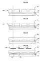
- FIG. 5 illustrates consecutive results of a double exposure patterning method according to the present invention including the effect of the first exposure and a first etching of the hard mask;
- FIG. 6 illustrates the results of a double exposure patterning method according to the present invention including the effect of the second exposure and a second etching of the hard mask;
- FIG. 7 illustrates a lithographic apparatus according to the invention.
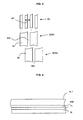
- FIG. 8 illustrates sizes of a feature of a target pattern, a mask pattern and a resist layer in relation to each other;
- FIG. 9 illustrates sizes of a feature of a target pattern, a mask pattern and a resist layer in relation to each other according to an embodiment of the present invention.
- the mask pattern may be embodied as a chrome on glass pattern substantially similar to the target pattern, i.e., the desired pattern.
- a mask pattern for example embodied as a quartz substrate provided with a pattern of features of chromium by means of electron beam writing, residual pattern-writing errors may occur. Such errors are by the lithographic process transferred in to the target pattern, and the sensitivity of a lithographic process to such pattern errors is expressed by a so called mask error factor. A reduction of mask error factor would provide an important advantage.
- MEF mask error factor
- the scaling factor M is or may not be mentioned, but is assumed to be accounted for when discussing dimensions at mask level.
- a resist patterning process is schematically indicated in Figure 8.
- a target pattern 800 comprising a periodic arrangement of a target feature 81 and an adjacent space 801 (which may, for example, be a line shaped feature 81 and an adjacent space 801) is to be printed in positive tone resist, provided as a layer 820 on a substrate.
- the pitch of the periodic arrangement is indicated by TP in Figure 8, and is referred to as the target pitch.
- a mask pattern 810 is illuminated and projected onto the substrate to expose the resist layer 820.
- the mask pattern 810 comprises a periodic arrangement of an object feature 82 and an adjacent space 802, in accordance with the target pattern.
- the object feature 82 has an object feature width PS, and the adjacent space 802 has a width of critical dimension CD of 25 nm. Further, the pitch at which the object feature and the adjacent space occur in the periodic arrangement 810 is referred to as the object pitch OP (hence, the relatively narrow spaces 802 are disposed at a pitch OP). In the present process the pitch OP is 100 nm. Thus, the object features 82 have a width of 75 nm, i.e., three times the critical dimension CD.
- the exposure process may for example be executed using an attenuated Phase Shift Mask (att-PSM).
- the object features are embodied as phase shifting, radiation absorbing features (but passing a small percentage of the radiation), for example of molybdenum silicide (MoSi), with a width of three times the critical dimension CD, i.e., 75 nm, on a quartz substrate.
- the object features 82 are imaged as dark features in an image of the mask pattern at substrate level, and result in unexposed resist material features 83, whereas the spaces 802 are imaged as bright areas in the image, resulting in portions 803 of photoactivated resist.
- the periodic arrangement of the target pattern as described here can be further characterized by a target duty cycle TDC defined as target feature width TS divided by target pitch TP, referring to the dimensions of the features in the patterned resist layer, and a mask pattern duty cycle PDC, also referred to as object duty cycle or pattern duty cycle, defined as object feature width PS divided by object pitch OP, referring to the dimensions of the features at mask level.
- a parameter BR referred to as a bias-ratio, or ratio, or also as a bias
- Figure 9 schematically indicates the definition of the ratio BR.
- biasing of mask-pattern features may involves relative size deviations with respect to nominal size of up to about 10%.
- object duty cycle PDC which slightly deviates from the target duty cycle TDC.
- the pattern duty cycle PDC is 0.7 and the bias ratio BR is 0.93.
- deviations from unity of the bias-ratio BR are limited, however, to about + or - 0.1..
- FIG. 1 An example of the magnitude of the MEF, and typical for a process where the target pattern and the mask pattern are a periodic line and space pattern with a bias ratio BR between 0.9 and 1.1, is illustrated in Figure 1.
- the horizontal axis indicates the width PS of the lines of the mask pattern
- the vertical axis indicates the resulting width 83 of the lines as patterned in resist, ideally corresponding to the target width TS.
- the tangent of the slope-angle A of the plot of the width 83 versus the width PS in Figure 1 is representing the mask error factor for the present lithographic process.
- the value of MEF varies strongly with the width of the mask-pattern feature and is of the order of 10.
- the MEF of this process can be substantially reduced by selecting a value of the bias-ratio BR which is lower than 0.8.
- the bias-ratio is chosen to be 0.67. This implies that both the lines and the spaces at the mask are embodied as lines and spaces of 50 nm width.
- the object duty cycle PDC is 0.5
- the required target duty cycle TDC is 0.75.
- Figure 2 illustrates the resulting sensitivity to mask pattern errors under the same illumination conditions as described above.
- the MEF is reduced to a value in a range between 2.9 and 3.8.
- the bias of the object feature 82 is applied asymmetrically with respect to the position of the target feature. It is appreciated that the invention is not limited to such an asymmetric bias, but that the bias can be disposed differently and in particular the bias can be arranged symmetric with respect to the corresponding target feature.
- the compensating includes adjusting the exposure dose to compensate for the pattern duty cycle PDC being set at 0.5 instead of 0.75.
- Such an adjustment of exposure dose causes an adjustment of the exposure dose within exposed areas of the pattern of the radiation at substrate level.
- this pattern can be considered as an image in air, as provided by the projection system.
- the concept of "energy-to-clear” is related to a change of solubility from insoluble to soluble in a positive tone resist (and from soluble to insoluble in a negative tone resist) which occurs at a threshold value of the exposure dose, the so-called energy-to-clear.
- the reduction of MEF as obtained according to the present invention also leads to a reduction of LER, since a line edge roughness error in the processed target pattern is dependent on a line edge roughness of the lines comprised in the mask pattern.
- a second embodiment is the same as the first embodiment, safe that the target duty cycle TDC differs from 0.75.
- the advantages of the method according to the invention and as described in the first embodiment are substantially the same for semi dense target patterns of spaces adjacent to non-critically sized lines.
- the lines of the target pattern have a line width in the range of 70 nm to 80 nm, and the target pitch of the lines and spaces is 100 nm.
- the value of target duty cycle TDC may, in accordance with the present invention, be selected from a range of values 0.7 to 0.8.
- this range of target pattern line widths may be provided using mask pattern line widths in the range of 20 nm to 55 nm at a pitch of 100 nm (ignoring the scale factor M) in combination with an adjustment of the exposure dose to maintain any of the selected target pattern duty cycles, i.e., with the pattern duty cycle PDC having a value in the range 0.2 to 0.55.
- the bias ratio BR has, in the present embodiment, a lowest value of 0.25 and a highest value of 0.78, i.e., below 0.8.
- the concept of a "space" comprised by a pattern of lines and spaces in resist is not limited to a space as obtained after development of the resist.
- the advantages of the invention are obtained irrespective of lithographic processing after exposure, such as for example a post exposure bake and a development of the resist.
- the lines of the target pattern are lines of unexposed positive tone resist material, and the spaces of the target pattern are embodied as portions of photo activated positive tone resist material, where these portions are shaped in accordance with the spaces of the target pattern.
- the bias ratio BR is 0.5, and the obtainable MEF is 2.
- a negative tone resist (instead of a positive tone resist) may be used in any of the first four embodiments, when instead of the spaces in these embodiments corresponding features of exposed negative tone resist material (and protruding from a surface of the substrate after development of the unexposed resist) have to be provided. Since then the imaging of the mask pattern is substantially the same as in the first four embodiments, a similar reduction of MEF is obtained.
- the compensating for the applied bias in any of the first four embodiments includes developing (dissolving) of exposed resist and applying a feature shrink process, or a combination of exposure dose adjustment and applying a feature shrink after development.
- the feature shrink process may be arranged to reduce the width of the spaces of the pattern obtained upon resist development.
- the shrinking of the spaces is provided by applying a chemical processing (such as overcoating the spaces with RELACS TM material, applying a mixing/bake process, cooling the substrate and rinsing by D.I. water) or a thermal resist flow processing for shrinking features can be used and have been shown to enable feature size correction of up to 50 nm shrink in a controlled way.
- PEB Post Exposure Bake
- a resist pattern obtained after developing the resist may serve as an etch mask for etching a hard mask disposed underneath the resist layer.
- the lithographic dual exposure patterning process involves the exclusive use of positive tone resist for printing features whereby k 1 ⁇ 0.25.
- positive tone resist is preferable over the use of negative tone resist for lithographic printing of features such as, for example, dense, semi dense and/or isolated lines.
- the method of patterning a resist layer as described in any of the first three embodiments is applied twice in a double exposure lithographic process.
- the invention comprises decomposing a desired pattern of dense CD-sized features and CD-sized spaces (such as for example, dense lines and spaces) into a first and second target pattern of semi dense, CD-sized spaces (and non-critically sized features or lines).
- the spaces are printed in interposed or interlaced position with respect to each other, using positive tone resist for each exposure.
- Two mask patterns, or object patterns are associated with the two respective target patterns, and the respective object patterns may be disposed on a single reticle or on two separate reticles.
- each of the exposures is preceded by applying a bias ratio BR to the object features of the two object patterns to a value lower than 0.8, so that the duty cycle PDC of the two object patterns is lower than 0.6.
- CD-sized spaces of the target patterns correspond to relative space-width widened spaces of the two corresponding mask patterns of semi dense spaces, whereby a factor representative for the space-width widening has a value between 1 and 3 (ignoring the demagnification factor of a projection system), thereby reducing mask error factor and line edge roughness.
- Figure 3 illustrates a periodic arrangement of a desired feature (a line) 31 and an adjacent , desired space 301; the pitch DP of the periodic arrangement is the desired pitch of the pattern DL.
- the desired pattern DL is split into two, interposed target patterns, respectively a first target pattern SDS 1 and a second target pattern SDS2.
- rule based or model based mask pattern design software may be used.
- Each of the target patterns SDS 1 and SDS2 include a periodic arrangement of a respective target line feature 32, 34 and a respective target space 302, 304 adjacent to the target feature.
- the width of the target space (302, 304) is identical to the width of the desired space 301, as illustrated in Figure 3.
- the method comprises two successive positive tone resist layer patternings, whereby the spaces 302 and 304 of two the respective target patterns SDS 1 and SDS2, are positioned in interlaced position with respect to each other on the substrate.
- the patterns SDS 1 and SDS2 may be transferred to the material layer to provide the desired pattern DL.
- the substrate W which may carry previously processed IC layers, is provided with a target layer TL, a hard mask layer HM on top of the target layer TL, and a positive tone resist layer RL 1 on top of the hard mask layer HM.
- the first patterning with a target pattern SDS 1 having a target duty cycle TDC1 includes providing a mask pattern MP1 in accordance with the target pattern SDS1, and having an object duty cycle PDC1, and a bias-ratio BR1.
- the bias-ratio BR1 is chosen lower than 0.8.
- the successive exposure conditions are the same as in the first embodiment.
- the target duty cycles TDC1 and TDC2 of the respective target patterns SDS 1 and SDS2 are both 0.75
- the object duty cycles PDC1 and PDC2 of the respective mask patterns MP1 and MP2 are both 0.5
- the respective bias-ratios BR1 and BR2 for the features of both masks is 0.67.
- the resist layer RL 1 is exposed to a pattern of the radiation using the mask pattern MP1 and the projection system which are arranged to image the mask pattern onto the resist layer.
- the exposure dose is adjusted to arrive at the target duty cycle TDC 1 as specified for the pattern SDS 1.
- the first patterning is followed by developing the resist layer RL1 to provide an etch mask RM1 of resist material, as illustrated in Figure 5A.
- the hard mask layer HM is dry etched to transfer the target pattern to the hard mask layer, as illustrated in Figure 5B.
- the resist mask RM 1 is stripped, and a supplementary positive tone resist layer RL2 is applied to the hard mask layer HM, as illustrated in Figure 5C.
- the second exposure is executed the same way as described above, whereby the mask MP2 is positioned such that the spaces 304 of the target pattern SDS2 will be disposed in interlaced position with respect to the spaces of the pattern SDS1.
- This can be realized by arranging the spaces 502 of the mask MP2 in interlaced position with respect to the spaces 504 of the previously etched hard mask HM, as illustrated in Figure 5D.
- the advantage of low MEF is obtained by the choice of a bias ratio BR2 lower than 0.8, and by arranging the exposure dose in accordance with the selected bias-ratio BR2 to obtain the target duty cycle TDC2 as specified for the pattern SDS2.
- a subsequent development of the exposed resist layer RL2 provides an etch mask RM2 of resist material, as illustrated in Figure 6A.
- the hard mask layer HM is again dry etched to transfer the target pattern SDS2 to the hard mask layer, as illustrated in Figure 6B.
- the resist mask RM2 is then stripped, and as a result a transfer of the target pattern SDS 1 and the supplementary target pattern SDS2 is obtained such as to provide a patterning of the hard mask HM which corresponds to the desired pattern DL, as illustrated in Figure 6C.
- a final pattern transfer which can be part of the previous pattern transfer in an integrated etch chamber, is obtained by applying a third etching of the target layer TL.
- the providing the resist-masks RM 1 and RM2 may further include a variety of processes before and/or after exposure of the resist layer.
- pre-exposure processes may include cleaning, priming, and soft bake processes.
- the wafer substrates may be subjected to different post-exposure processes, such as, for example, a post exposure bake (PEB), and a hard bake.
- PEB post exposure bake
- any photoresist layer may include a Bottom Anti Reflection Coating or a Developable Bottom Anti Reflection Coating to reduce back reflection of exposure radiation.
- a sixth embodiment of the invention is the same as the fifth embodiment safe for the developing of the resist layer RL1 after the first exposure, and the subsequent etching of the hard mask layer HM and stripping of the resist mask RM1.
- the resist layer RL 1 is subjected to a post exposure bake and next the (substantially) unexposed portions of the resist layer RL 1 are subjected to a supplementary, second exposure in accordance with the second exposure process of the previous embodiment.
- the post exposure bake has the effect of fixing the first target pattern SDS1 in the resist layer RL1, so that during the second exposure the resist has no "memory" of the first exposure. Non linear chemical properties of the resist are exploited for said fixing the pattern.
- positive tone resists for use with KrF excimer lasers and ArF excimer lasers are chemically amplified resists.
- a critical component of chemically amplified resist materials is the photo-acid generator (referred to as PAG), which is the photo-active ingredient.
- the resist further comprises a base B compound in a blocked matrix configuration. In this configuration, after exposure, photo-acid generator PAG is converted into a photo-acid PA+, of which some is neutralized by the base B compound.
- a reaction is catalyzed between the photo-acid PA+ and the polymer so that, after baking, the polymer is deblocked, rendering it soluble in typical developer solutions, and the photo-acid PA+ is largely dissipated.
- the photo-induced polymer deblocking reaction may cease, i.e. loses memory of the initial exposure, after approximately 40 seconds of baking time.
- the chemical reactions occurring between the photo-acid PA+ and the polymer are reduced such that the extent of polymer deblocking does not increase with longer baking times.
- the photo-acid PA+ virtually dissipates to provide a relatively high contrast and stable latent image corresponding to the pattern SDS 1 on a photoresist that further has little memory of the first (or any other any preceding) exposure.
- the spatial Fourier transformation of the features of the resist-mask RM 1 corresponding to the pattern SDS1 contain higher spatial frequencies than the spatial Fourier transformation of the intensity pattern of the image of the mask-pattern MP1, as provided by the projection system of the lithographic apparatus.
- the intensity pattern of the image of the mask-pattern MP2 contain lower spatial frequencies than the spatial Fourier transformation of the features of mask-pattern MP1.
- target duty cycles may have a value between 0.7 and 0.8
- pattern duty cycles may have a value between 0.2 and 0.55.
- any of the embodiments described above is not limited to patterns comprising lines and spaces.
- the invention is generally applicable to printing features such as for example trenches arranged in semi dense patterns (using single exposure processes according to the present invention) and dense patterns of trenches (using double exposure processes according to the present invention).
- a seventh embodiment is the same as the fifth embodiment safe for the details described below.
- a double exposure printing method uses two exposures as described in the fourth embodiment, whereby a further reduction of MEF down to a value of 2 is provided with each exposure.
- the seventh embodiment further differs from the fifth embodiment in that the etching step between the two exposures and the etching step after the second exposure are each supplemented by applying a feature shrink process.
- the feature shrink step is arranged to reduce the width of the spaces of the patterns SDS 1 and SDS2 for example, down to 30 nm, enabling the interlaced positioning of the spaces, as described in the fifth embodiment.
- a feature shrink can be arranged and obtained by applying an etch bias to a process of dry etching the hard mask layer HM.
- the shrinking is provided by applying a resist-processing to shrink the features of the resist masks RM 1 and RM2.
- Resist process shrink techniques such as, for example, a chemical and a thermal resist processing for shrinking features can be used and have been shown to enable feature size correction of up to 50 nm shrink in a controlled way.
- the present exposure and line printing method in principle only uses a conventional aqueous development steps and dry etch steps. Consequently, the present method can easily be implemented in a lithographic system comprising the lithographic apparatus and a coat/develop track that is typically linked to the lithographic apparatus.
- a lithographic exposure apparatus according to an embodiment of the invention is schematically depicted in Figure 7.
- the apparatus comprises:
- an illumination system (illuminator) IL configured to condition a radiation beam B (e.g., UV radiation or DUV radiation such as for example generated by an excimer laser operating at a wavelength of 193 nm or 157 nm, or EUV radiation generated by a laser-fired plasma source operating at 13,6 nm).
- a radiation beam B e.g., UV radiation or DUV radiation such as for example generated by an excimer laser operating at a wavelength of 193 nm or 157 nm, or EUV radiation generated by a laser-fired plasma source operating at 13,6 nm.
- a support structure e.g., a mask table
- MT constructed to support a patterning device (e.g., a mask) MA and connected to a first positioner PM configured to accurately position the patterning device in accordance with certain parameters;
- a substrate table e.g., a wafer table
- WT constructed to hold a substrate (e.g., a resist-coated wafer) W and connected to a second positioner PW configured to accurately position the substrate in accordance with certain parameters
- a projection system e.g., a refractive projection lens system
- PS configured to project a pattern imparted to the radiation beam B by patterning device MA onto a target portion C (e.g., comprising one or more dies) of the substrate W.
- the illumination system may include various types of optical components, such as refractive, reflective, magnetic, electromagnetic, electrostatic or other types of optical components, or any combination thereof, for directing, shaping, or controlling radiation.
- optical components such as refractive, reflective, magnetic, electromagnetic, electrostatic or other types of optical components, or any combination thereof, for directing, shaping, or controlling radiation.
- the support structure may be a frame or a table, for example, which may be fixed or movable as required.
- the support structure may ensure that the patterning device is at a desired position, for example with respect to the projection system. Any use of the terms "reticle” or “mask” herein may be considered synonymous with the more general term “patterning device.”
- patterning device used herein should be broadly interpreted as referring to any device that can be used to impart a radiation beam with a pattern in its cross-section such as to create a pattern in a target portion of the substrate. It should be noted that the pattern imparted to the radiation beam may not exactly correspond to the desired pattern in the target portion of the substrate, for example if the pattern includes phase-shifting features or so called assist features. Generally, the pattern imparted to the radiation beam will correspond to a particular functional layer in a device being created in the target portion, such as an integrated circuit.
- the patterning device may be transmissive or reflective.
- projection system used herein should be broadly interpreted as encompassing any type of projection system, including refractive, reflective, and catadioptric optical systems, or any combination thereof, as appropriate for the exposure radiation being used, or for other factors such as the use of an immersion liquid or the use of a vacuum. Any use of the term “projection lens” herein may be considered as synonymous with the more general term “projection system”.
- the apparatus is of a transmissive type (e.g., employing a transmissive mask).
- the apparatus may be of a reflective type (e.g., employing a reflective mask).
- the lithographic apparatus may be of a type having two (dual stage) or more substrate tables (and/or two or more mask tables). In such "multiple stage” machines the additional tables may be used in parallel, or preparatory steps may be carried out on one or more tables while one or more other tables are being used for exposure.
- the lithographic apparatus may also be of a type wherein at least a portion of the substrate may be covered by a liquid having a relatively high refractive index, e.g., water, so as to fill a space between the projection system and the substrate.
- a liquid having a relatively high refractive index e.g., water
- An immersion liquid may also be applied to other spaces in the lithographic apparatus, for example, between the mask and the projection system. Immersion techniques are well known in the art for increasing the numerical aperture of projection systems.
- immersion as used herein does not mean that a structure, such as a substrate, must be submerged in liquid, but rather only means that liquid is located between the projection system and the substrate during exposure.
- the illuminator IL receives a radiation beam from a radiation source SO.
- the source and the lithographic apparatus may be separate entities, for example when the source is an excimer laser. In such cases, the source is not considered to form part of the lithographic apparatus and the radiation beam is passed from the source SO to the illuminator IL with the aid of a beam delivery system BD comprising, for example, suitable directing mirrors and/or a beam expander. In other cases the source may be an integral part of the lithographic apparatus, for example when the source is a mercury lamp.
- the source SO and the illuminator IL, together with the beam delivery system BD if required, may be referred to as a radiation system.
- the illuminator IL may comprise an adjuster AD for adjusting the angular intensity distribution of the radiation beam. Generally, at least the parameters ⁇ -outer and ⁇ -inner, respectively, of the intensity distribution in a pupil plane of the illuminator can be adjusted.
- the illuminator IL may comprise various other components, such as an integrator IN and a condenser CO. The illuminator may be used to condition the radiation beam, to have a desired uniformity and intensity distribution in its cross-section.
- the radiation beam B is incident on the patterning device (e.g., mask MA), which is held on the support structure (e.g., mask table MT), and is patterned by the patterning device. Having traversed the mask MA, the radiation beam B passes through the projection system PS, which focuses the beam onto a target portion C of the substrate W.
- the substrate table WT can be moved accurately, e.g., so as to position different target portions C in the path of the radiation beam B.
- the first positioner PM and another position sensor can be used to accurately position the mask MA with respect to the path of the radiation beam B, e.g., after mechanical retrieval from a mask library, or during a scan.
- movement of the mask table MT may be realized with the aid of a long-stroke module (coarse positioning) and a short-stroke module (fine positioning), which form part of the first positioner PM.
- movement of the substrate table WT may be realized using a long-stroke module and a short-stroke module, which form part of the second positioner PW.
- the mask table MT may be connected to a short-stroke actuator only, or may be fixed.
- Mask MA and substrate W may be aligned using mask alignment marks M1, M2 and substrate alignment marks P1, P2.
- the substrate alignment marks as illustrated occupy dedicated target portions, they may be located in spaces between target portions (these are known as scribe-lane alignment marks).
- the mask alignment marks may be located between the dies.
- the depicted apparatus could be used in at least one of the following modes:
- step mode the mask table MT and the substrate table WT are kept essentially stationary, while an entire pattern imparted to the radiation beam is projected onto a target portion C at one time (i.e. a single static exposure).
- the substrate table WT is then shifted in the X and/or Y direction so that a different target portion C can be exposed.
- step mode the maximum size of the exposure field limits the size of the target portion C imaged in a single static exposure.
- the mask table MT and the substrate table WT are scanned synchronously while a pattern imparted to the radiation beam is projected onto a target portion C (i.e. a single dynamic exposure).
- the velocity and direction of the substrate table WT relative to the mask table MT may be determined by the (de-)magnification and image reversal characteristics of the projection system PS.
- the maximum size of the exposure field limits the width (in the non-scanning direction) of the target portion in a single dynamic exposure, whereas the length of the scanning motion determines the height (in the scanning direction) of the target portion.
- the mask table MT is kept essentially stationary holding a programmable patterning device, and the substrate table WT is moved or scanned while a pattern imparted to the radiation beam is projected onto a target portion C.
- a pulsed radiation source is employed and the programmable patterning device is updated as required after each movement of the substrate table WT or in between successive radiation pulses during a scan.
- This mode of operation can be readily applied to maskless lithography that utilizes programmable patterning device, such as a programmable mirror array of a type as referred to above.
- the lithographic system comprises, as lithographic exposure apparatus, a lithographic interferometric apparatus.
- a resist layer is exposed to a fringe pattern obtained in a multiple beam interferometric apparatus.
- two collimated beams of UV or DUV radiation intersect each other at an angle to produce linear interference fringes.
- a wafer having a photosensitive layer is positioned on a movable table. The table is arranged to be rotated and translated in two-dimensions respectively.
- Two substantially collimated coherent optical beams provided by any suitable well known source or sources are directed at a variable angle from the normal vector associated with the wafer toward each other and toward the photoresist layer to form an interference pattern on the photosensitive layer.
- the interfering radiation beams of coherent radiation may be generated by, for example, an ArF excimer laser using a beam splitting element, and may be provided in any suitable well known manner so that they are from the same source and are essentially equal in intensity at the wafer which assures a high contrast exposure.
- the interference pattern produced on the photoresist layer or layers may be varied by for example rotating the wafer and/or translating the wafer.
- a control device may comprise a memory into which data can be stored which concern the sub-patterns SDS 1 and SDS2 and which are used for controlling the lithographic exposure apparatus (such as, for example, settings concerning positioning of the stages MT and WT, and/or settings concerning illumination modes) during each of the two exposures required to generate the combined pattern DL.
- the same memory can be used to store data concerning the settings bias-ratios BR1 and BR2.
- a computer which may be part of the control device is programmed and arranged to execute, based on the data stored in the memory, any of the method steps according to the present invention.
- a computer program product may comprise program code to control a lithographic apparatus to perform a method of patterning a resist layer, overlaying at least partially a substrate, with a target pattern comprising a periodic arrangement of a target feature and an adjacent space, the target feature having a target feature width.
- the method includes illuminating a mask pattern comprising a periodic arrangement of an object feature and an adjacent space, the object feature having an object feature width, projecting the mask pattern at a demagnification onto a substrate, exposing a resist layer, overlaying at least partially the substrate, to an image of the mask pattern wherein each of the object features is imaged at a brightness lower than the brightness of respective adjacent spaces, and compensating for a bias ratio being lower than 0.8, wherein the bias ratio is defined as the object feature width multiplied by the demagnification and divided by the target feature width.
- a lithographic apparatus comprises a controller configured to run the computer program product and to effect the compensating.
- the lithographic apparatus is configured to execute a dual exposure process such as for example described in the fifth embodiment.
- the above described controller of the lithographic apparatus is then configured to run the computer program product described above and to effect the compensating for two different resist patterning processes wherein a first resist layer is patterned with a first target pattern including a periodic arrangement of a target feature and an adjacent space and a second resist layer is patterned with a second target pattern including a periodic arrangement of a target feature and an adjacent space, and wherein the spaces of the first and second target patterns are interposed.
- lithographic apparatus in the manufacture of ICs
- the lithographic apparatus described herein may have other applications, such as the manufacture of integrated optical systems, guidance and detection patterns for magnetic domain memories, flat-panel displays, liquid-crystal displays (LCDs), thin-film magnetic heads, etc.
- LCDs liquid-crystal displays
- any use of the terms “wafer” or “die” herein may be considered as synonymous with the more general terms “substrate” or "target portion”, respectively.
- the substrate referred to herein may be processed, before or after exposure, in for example a track (a tool that typically applies a layer of resist to a substrate and develops the exposed resist), a metrology tool and/or an inspection tool. Where applicable, the disclosure herein may be applied to such and other substrate processing tools. Further, the substrate may be processed more than once, for example in order to create a multi-layer IC, so that the term substrate used herein may also refer to a substrate that already contains multiple processed layers.
- UV radiation e.g., having a wavelength of or about 365, 355, 248, 193, 157 or 126 nm
- EUV radiation e.g., having a wavelength in the range of 5-20 nm
- lens may refer to any one or combination of various types of optical components, including refractive, reflective, magnetic, electromagnetic and electrostatic optical components.
Landscapes
- Physics & Mathematics (AREA)
- General Physics & Mathematics (AREA)
- Exposure And Positioning Against Photoresist Photosensitive Materials (AREA)
- Exposure Of Semiconductors, Excluding Electron Or Ion Beam Exposure (AREA)
Abstract
A single exposure method and a double exposure method for reducing mask error factor and for enhancing lithographic printing-process resolution is presented. The invention comprises decomposing a desired pattern of dense lines and spaces in two sub patterns of semi dense spaces that are printed in interlaced position with respect to each other, using positive tone resist. Each of the exposures is executed after applying a relative space-width widening to the spaces of two corresponding mask patterns of semi dense spaces. A factor representative for the space-width widening has a value between 1 and 3, thereby reducing mask error factor and line edge roughness.
Description
- The present invention generally relates to photolithography and associated methods for exposing semiconductor substrates.
- Lithographic exposure apparatuses can be used, for example, in the manufacture of integrated circuits (ICs). In such a case, a patterning device (e.g. a mask or reticle provided with a mask pattern) may generate a circuit pattern corresponding to an individual layer of the IC. In photolithography, a beam of radiation is patterned by having that beam traverse the reticle, and is projected by a projection system of the lithographic apparatus onto a target portion (e.g., comprising one or more dies) on a substrate (silicon wafer) that has been coated with a layer of photo-active resist (i.e., photoresist) material, such as to image a desired pattern in the resist. In general, a single wafer will contain a whole network of adjacent target portions that are successively irradiated via the projection system, one at a time.
- In the semiconductor industry, the continual demand for smaller semiconductor devices, having smaller patterns and features on the wafer substrate, is pushing the limits on the optical resolution that can be achieved by lithographic exposure apparatus.
- Generally, the smallest size of a repeatable feature (e.g., "half-pitch") of a pattern exposed on the wafer substrate that can be optically resolved by lithographic exposure apparatus, depends on attributes of the projection system and the (patterned) projection beam of radiation. In particular, the optical resolution for half-pitch feature size may be derived by using the simplified form of the Rayleigh resolution equation:

- where: p0.5 represents the repeatable feature size (e.g., "half-pitch") in nm;
- NA represents the numerical aperture of projection system;
- λ represents the wavelength of projection beam, in nm; and
- k1 is a factor representative for the achievable optical resolution limit for the half-pitch feature size.
- As indicated above, the theoretical optical resolution half-pitch lower limit for k1 is 0.25. In an attempt to approach the k1 = 0.25 barrier, considerable efforts have been directed to develop expensive technologies that are capable of employing shorter wavelengths and/or higher numerical apertures, thus allowing production of smaller features approaching the k1 ≥0.25 constraint.
- Fabrication of an integrated circuit pattern involves the control of space tolerances between features, as well as control of feature dimension tolerances. In particular the control of tolerances of the smallest dimensions such as for example the sizes of contacts or the width of lines or of spaces between lines permitted in the fabrication of the integrated circuit device is of importance. The size of these most critical dimensions is referred to as the critical dimension ("CD"). Features comprising a minimum size substantially equal to the CD are referred to as "CD-sized features" in the present text.
- Further, a variety of phenomena that accompany low k1 imaging, such as line-end retraction, corner rounding, variation of CD versus pitch, mask error factor ("MEF"), and line-edge roughness ("LER") may lead to a loss of feature fidelity beyond tolerance. In particular, MEF contributes to variations in lengths of polysilicon gates, reducing performance of the integrated circuit. The MEF is defined as the ratio of a change in CD of CD-sized features in resist in response to a change of the corresponding size of the corresponding features on the mask, whereby the latter size is normalized to substrate level taking into account a demagnification of the projection system. In the field of photolithography, Mask Error Factor is, alternatively, also referred to as Mask Error Enhancement Factor ("MEEF"). The two concepts are identical, and in the present text referred to as Mask Error Factor or MEF.
- Lithographic apparatus as mentioned above typically include a radiation system and a projection system. The radiation system generally includes an illumination system. The illumination system receives radiation from a source, such as a laser, and produces an illumination beam for illuminating an object, such as the patterning device (e.g., a mask on a mask table). Within a typical illumination system, the beam is shaped and controlled such that at a pupil plane of the illumination system the beam has a desired spatial intensity distribution. Such a spatial intensity distribution at the pupil plane effectively acts as a virtual radiation source for producing the illumination beam. Various shapes of said intensity distribution, consisting of (substantially uniform) light areas on a dark background, can be used. Any such shape will be referred to hereinafter as an "illumination mode". Known illumination modes include: conventional (a top-hat shaped intensity distribution in said pupil), annular, dipole, quadrupole and more complex shaped arrangements of the illumination pupil intensity distribution. A lateral position in said pupil plane corresponds to an angle of incidence at the patterning device, and any such angle of incidence is commonly expressed as a fraction sigma (σ) of a numerical aperture NA of the projection system. Therefore, a more complete characterization of the intensity distribution in a pupil of the illumination system involves, besides an indication of the illumination mode, also an indication of parameters of the illumination mode, such as, for example, σ and NA. A combination of an illumination mode and corresponding parameters of said illumination mode is referred to hereinafter as an "illumination setting". Known illumination settings include: a "conventional" illumination setting (whereby the intensity distribution in an illumination pupil is substantially uniform up to a certain radius defined by a parameter value of σ, where 0 < σ < 1, and a parameter value of the numerical aperture NA of the projection system), an annular setting, a dipole setting, a quadrupole setting and more complex arrangements. An annular or a multipole setting are typically characterized by the parameters σinner and σouter respectively indicating an inner and outer radial extent of an annulus or of poles. Such illumination modes are providing off-axis illumination of a patterning device. Illumination settings may be formed in various ways. The σ value of a conventional illumination mode can be controlled using a zoom lens while σinner and σouter values of an annular mode can be controlled using a zoom-axicon. The NA value can be controlled using a settable iris diaphragm in the projection system.
- More complex settings (such as said dipole and quadrupole modes) may be formed using a diaphragm with appropriate apertures in the pupil plane or by a diffractive optical element. Typically, said diffractive optical element is arranged to generate a preselected angular intensity distribution upstream of a pupil plane of the illumination system. This angular intensity distribution is transformed into a corresponding spatial intensity distribution in the pupil plane of the illumination system.
- In particular at high numerical aperture (NA > 0.85) and using off axis illumination modes for illumination the patterning device, MEF and LER are most prominent errors limiting a further reduction of k1 for those lithographic processes whereby the task is to print in resist semi-dense regularly spaced patterns of trenches or lines, the width sized at critical dimension and the features spaced apart about three times the critical dimension.
- Embodiments of the present invention ameliorate a lithographic exposure process for patterning a resist layer. A method consistent with the principles of the present invention, as embodied and broadly described herein, provide for the enhancement of image resolution in a lithographic system.
- There is provided a method of patterning a resist layer, overlaying at least partially a lithographic substrate, with a target pattern comprising a periodic arrangement of a target feature and an adjacent space, the target feature having a target feature width, including illuminating a mask pattern comprising a periodic arrangement of an object feature and an adjacent space, the object feature having an object feature width, projecting the mask pattern at a demagnification onto the substrate, exposing the resist layer to an image of the mask pattern wherein each of the object features is imaged at a brightness lower than the brightness of respective adjacent spaces, and wherein the method further includes arranging a ratio, defined as the object feature width multiplied by the demagnification and divided by the target feature width, at a value lower than 0.8, and compensating for the ratio being lower than 0.8 to provide the target pattern.
- According to an aspect of the invention there is provided a second method which is a method as described above wherein the periodic arrangement of the target pattern has a target pitch and wherein a target duty cycle, defined as the target feature width divided by the target pitch, is one of any value between 0.7 and 0.8
- According to an aspect of the invention there is provided a method of providing a substrate with a desired pattern comprising a periodic arrangement of a desired feature and an adjacent desired space, including: splitting the desired pattern in two interposed target patterns, respectively a first target pattern and a second target pattern, each target pattern comprising a periodic arrangement of a target feature with the desired space disposed adjacent to the target feature; providing a first resist layer to the substrate, overlaying at least partially the substrate, patterning the first resist layer with the first target pattern according to the second method described above, developing the first resist layer; providing a second resist layer to the substrate, overlaying at least partially the substrate, patterning the second resist layer with the second target pattern according to the second method described above, wherein the projecting is arranged to position the spaces of the second target pattern in interposed relation to the spaces of the of the first target pattern.
- According to another aspect of the invention there is provided a computer program product comprising program code to control a lithographic apparatus to perform a method of patterning a resist layer, overlaying at least partially a substrate, with a target pattern comprising a periodic arrangement of a target feature and an adjacent space, the target feature having a target feature width, comprising illuminating a mask pattern comprising a periodic arrangement of an object feature and an adjacent space, the object feature having an object feature width, projecting the mask pattern at a demagnification onto a substrate, exposing a resist layer, overlaying at least partially the substrate, to an image of the mask pattern wherein each of the object features is imaged at a brightness lower than the brightness of respective adjacent spaces, and compensating for a bias ratio being lower than 0.8, wherein the bias ratio is defined as the object feature width multiplied by the demagnification and divided by the target feature width.
- According to a further aspect of the invention there is provided a lithographic apparatus comprising a controller configured to run the computer program product and to effect the compensating as described above.
- Embodiments of the invention will now be described, by way of example only, with reference to the accompanying schematic drawings in which corresponding reference symbols indicate corresponding parts, and in which:
- - Figure 1 illustrates a magnitude of mask error factor for a lithographic patterning process. The horizontal axis indicates a width of lines of a mask pattern, and the vertical axis indicates a width of lines as patterned in resist;
- - Figure 2 illustrates a magnitude of mask error factor for a lithographic patterning process according to the present invention;
- - Figure 3 illustrates a decomposition of a desired pattern of dense lines and spaces into two patterns of semi dense spaces;
- - Figure 4 illustrates a lithographic substrate provided with a hard mask and a resist layer;
- - Figure 5 illustrates consecutive results of a double exposure patterning method according to the present invention including the effect of the first exposure and a first etching of the hard mask;
- - Figure 6 illustrates the results of a double exposure patterning method according to the present invention including the effect of the second exposure and a second etching of the hard mask;
- - Figure 7 illustrates a lithographic apparatus according to the invention.
- - Figure 8 illustrates sizes of a feature of a target pattern, a mask pattern and a resist layer in relation to each other; and
- - Figure 9 illustrates sizes of a feature of a target pattern, a mask pattern and a resist layer in relation to each other according to an embodiment of the present invention.
- As noted above, there exists a constant need to achieve finer optical resolutions thereby approaching the theoretical half-pitch lower limit k1 of 0.25, for printing patterns of features and spaces between the features, such as, for example, dense or semi dense patterns of lines and spaces. Besides enhancing the resolution of the lithographic patterning process, there is a need to maintain feature fidelity. The mask pattern may be embodied as a chrome on glass pattern substantially similar to the target pattern, i.e., the desired pattern. However, during the manufacturing of a mask pattern, for example embodied as a quartz substrate provided with a pattern of features of chromium by means of electron beam writing, residual pattern-writing errors may occur. Such errors are by the lithographic process transferred in to the target pattern, and the sensitivity of a lithographic process to such pattern errors is expressed by a so called mask error factor. A reduction of mask error factor would provide an important advantage.
- As noted above the phenomenon of mask error factor (MEF) accompanying low k1 imaging, may lead to a loss of feature fidelity beyond tolerance. The MEF is defined as the ratio of a change ΔRS of a CD-sized feature width RS in resist, in response to a change ΔPS of a corresponding size PS of the corresponding features on the mask, whereby the latter size PS is normalized to substrate level taking into account the demagnification M of the projection system (the magnitude of M may for example be 1/4, 1/5 or 1/8):

- For simplicity, in the present text and formula's the scaling factor M is or may not be mentioned, but is assumed to be accounted for when discussing dimensions at mask level. In the presence of a mask error factor the feature fidelity as provided by the imaging process using the projection system in combination with the imaging properties of the exposed resist may become affected such as to become beyond tolerance. Below, in formula's and figures M is set equal to 1; however, it is appreciated that the present invention is not limited to processes and apparatus wherein M=1.
- To illustrate the occurrence of MEF, a resist patterning process is schematically indicated in Figure 8. In the process a
target pattern 800, comprising a periodic arrangement of atarget feature 81 and an adjacent space 801 (which may, for example, be a line shapedfeature 81 and an adjacent space 801) is to be printed in positive tone resist, provided as alayer 820 on a substrate. The pitch of the periodic arrangement is indicated by TP in Figure 8, and is referred to as the target pitch. Amask pattern 810 is illuminated and projected onto the substrate to expose the resistlayer 820. Themask pattern 810 comprises a periodic arrangement of anobject feature 82 and anadjacent space 802, in accordance with the target pattern. Theobject feature 82 has an object feature width PS, and theadjacent space 802 has a width of critical dimension CD of 25 nm. Further, the pitch at which the object feature and the adjacent space occur in theperiodic arrangement 810 is referred to as the object pitch OP (hence, the relativelynarrow spaces 802 are disposed at a pitch OP). In the present process the pitch OP is 100 nm. Thus, the object features 82 have a width of 75 nm, i.e., three times the critical dimension CD. The exposure process may for example be executed using an attenuated Phase Shift Mask (att-PSM). With such a mask, the object features are embodied as phase shifting, radiation absorbing features (but passing a small percentage of the radiation), for example of molybdenum silicide (MoSi), with a width of three times the critical dimension CD, i.e., 75 nm, on a quartz substrate. The object features 82 are imaged as dark features in an image of the mask pattern at substrate level, and result in unexposed resist material features 83, whereas thespaces 802 are imaged as bright areas in the image, resulting inportions 803 of photoactivated resist. - The periodic arrangement of the target pattern as described here can be further characterized by a target duty cycle TDC defined as target feature width TS divided by target pitch TP, referring to the dimensions of the features in the patterned resist layer, and a mask pattern duty cycle PDC, also referred to as object duty cycle or pattern duty cycle, defined as object feature width PS divided by object pitch OP, referring to the dimensions of the features at mask level. For the present process, the duty cycles TDC and PDC are equal: TDC = PDC = 75 [nm] /100 [nm] = 0.75.
- To further characterize the lithographic patterning process, a parameter BR, referred to as a bias-ratio, or ratio, or also as a bias, is defined as the ratio of the object feature width scaled by the demagnification of the projection system, PS · M to the target feature width TS of the features of the target pattern:

and for the present process BR = 1 (M =1). Figure 9 schematically indicates the definition of the ratio BR. - Generally additional size deviations of mask-pattern features are introduced to compensate, for example, effects of errors occurring during projection and exposure of a pattern. Such biasing of mask-pattern features may involves relative size deviations with respect to nominal size of up to about 10%. Application of a bias results in an object duty cycle PDC which slightly deviates from the target duty cycle TDC. For example, when in the process described above the width of the spaces is increased by a factor 1.2, whilst the pitch of the spaces is kept at 100 nm, the pattern duty cycle PDC is 0.7 and the bias ratio BR is 0.93. Generally, deviations from unity of the bias-ratio BR are limited, however, to about + or - 0.1..
- An example of the magnitude of the MEF, and typical for a process where the target pattern and the mask pattern are a periodic line and space pattern with a bias ratio BR between 0.9 and 1.1, is illustrated in Figure 1. In Figure 1, the horizontal axis indicates the width PS of the lines of the mask pattern, and the vertical axis indicates the resulting
width 83 of the lines as patterned in resist, ideally corresponding to the target width TS. The tangent of the slope-angle A of the plot of thewidth 83 versus the width PS in Figure 1 is representing the mask error factor for the present lithographic process. The process is further characterized by a positive tone resist model which was calibrated for a NA of 0.93, a resist layer thickness of 50 nm, and a dipole TE polarized illumination mode with σinner = 0.82 and σouter = 0.96. The value of MEF varies strongly with the width of the mask-pattern feature and is of the order of 10. - According to a first embodiment of the present invention, the MEF of this process can be substantially reduced by selecting a value of the bias-ratio BR which is lower than 0.8. In the present embodiment the bias-ratio is chosen to be 0.67. This implies that both the lines and the spaces at the mask are embodied as lines and spaces of 50 nm width. The object duty cycle PDC is 0.5, and the required target duty cycle TDC is 0.75.
Figure 2 illustrates the resulting sensitivity to mask pattern errors under the same illumination conditions as described above. The MEF is reduced to a value in a range between 2.9 and 3.8. In the schematic illustration in Figure 9, the bias of theobject feature 82 is applied asymmetrically with respect to the position of the target feature. It is appreciated that the invention is not limited to such an asymmetric bias, but that the bias can be disposed differently and in particular the bias can be arranged symmetric with respect to the corresponding target feature. - In the present embodiment, the required target duty cycle TDC = 0.75 is obtained by compensating the patterning process for the applied bias of 0.67. The compensating includes adjusting the exposure dose to compensate for the pattern duty cycle PDC being set at 0.5 instead of 0.75. Such an adjustment of exposure dose causes an adjustment of the exposure dose within exposed areas of the pattern of the radiation at substrate level. For analysis purposes, this pattern can be considered as an image in air, as provided by the projection system. In the present embodiment, the contrast of the aerial image is much larger than the contrast of the aerial image in the conventional process, described above, whereby TDC = 0.75 and 0.9 < BR < 1.1. Therefore, a lowering of exposure dose with respect to the exposure dose in the prior art process can be exploited to broaden areas of the aerial image wherein exposure dose is below energy-to-clear. Here, the concept of "energy-to-clear" is related to a change of solubility from insoluble to soluble in a positive tone resist (and from soluble to insoluble in a negative tone resist) which occurs at a threshold value of the exposure dose, the so-called energy-to-clear. The reduction of MEF as obtained according to the present invention, also leads to a reduction of LER, since a line edge roughness error in the processed target pattern is dependent on a line edge roughness of the lines comprised in the mask pattern.
- A second embodiment is the same as the first embodiment, safe that the target duty cycle TDC differs from 0.75. The advantages of the method according to the invention and as described in the first embodiment are substantially the same for semi dense target patterns of spaces adjacent to non-critically sized lines. In this embodiment, the lines of the target pattern have a line width in the range of 70 nm to 80 nm, and the target pitch of the lines and spaces is 100 nm. Thus, the value of target duty cycle TDC may, in accordance with the present invention, be selected from a range of values 0.7 to 0.8. According to an aspect of the invention, this range of target pattern line widths may be provided using mask pattern line widths in the range of 20 nm to 55 nm at a pitch of 100 nm (ignoring the scale factor M) in combination with an adjustment of the exposure dose to maintain any of the selected target pattern duty cycles, i.e., with the pattern duty cycle PDC having a value in the range 0.2 to 0.55. With pattern line widths in the range of 20 nm to 55 nm at a pitch of 100 nm the bias ratio BR has, in the present embodiment, a lowest value of 0.25 and a highest value of 0.78, i.e., below 0.8.
- According to the invention the concept of a "space" comprised by a pattern of lines and spaces in resist is not limited to a space as obtained after development of the resist. The advantages of the invention are obtained irrespective of lithographic processing after exposure, such as for example a post exposure bake and a development of the resist.
- Consequently, in a third embodiment, which is the same as the first and or second embodiment, the lines of the target pattern are lines of unexposed positive tone resist material, and the spaces of the target pattern are embodied as portions of photo activated positive tone resist material, where these portions are shaped in accordance with the spaces of the target pattern.
- A further reduction of MEF is provided in a fourth embodiment of the invention, which is the same as the first embodiment safe that the pattern duty cycle PDC is PDC = 0.25 (pattern lines of 25 nm and pattern spaces of 75 nm) and the target duty cycle TDC = 0.5 (target pattern lines of 50 nm width and target pattern spaces of 50 nm width). The bias ratio BR is 0.5, and the obtainable MEF is 2.
- According to an aspect of the invention, a negative tone resist (instead of a positive tone resist) may be used in any of the first four embodiments, when instead of the spaces in these embodiments corresponding features of exposed negative tone resist material (and protruding from a surface of the substrate after development of the unexposed resist) have to be provided. Since then the imaging of the mask pattern is substantially the same as in the first four embodiments, a similar reduction of MEF is obtained.
- According to another aspect of the invention, the compensating for the applied bias in any of the first four embodiments includes developing (dissolving) of exposed resist and applying a feature shrink process, or a combination of exposure dose adjustment and applying a feature shrink after development. The feature shrink process may be arranged to reduce the width of the spaces of the pattern obtained upon resist development. For example, the shrinking of the spaces is provided by applying a chemical processing (such as overcoating the spaces with RELACS™ material, applying a mixing/bake process, cooling the substrate and rinsing by D.I. water) or a thermal resist flow processing for shrinking features can be used and have been shown to enable feature size correction of up to 50 nm shrink in a controlled way.
- As noted above, there exists a constant need to achieve finer optical resolutions. According to the present invention it is possible to circumventing the theoretical half-pitch lower limit k1 of 0.25 for printing dense lines using a double exposure process and exploiting the advantages of the single exposure embodiments described above.
- As described in greater detail below, the present invention achieves resolutions lower than the half-pitch lower limit half pitch p0.5 = k1 • λ/NA whereby k1 = 0.25, thus circumvention the k1 = 0.25 barrier, by implementing a dual exposure technique wherein between the two exposures a Post Exposure Bake (also referred to as "PEB") of the resist is applied, or alternatively, a Post Exposure Bake in combination with a subsequent development of the resist is applied. A resist pattern obtained after developing the resist may serve as an etch mask for etching a hard mask disposed underneath the resist layer.
- According to an aspect of the invention the lithographic dual exposure patterning process involves the exclusive use of positive tone resist for printing features whereby k1 < 0.25. The use of positive tone resist is preferable over the use of negative tone resist for lithographic printing of features such as, for example, dense, semi dense and/or isolated lines.
- According to an aspect of the invention, the method of patterning a resist layer as described in any of the first three embodiments is applied twice in a double exposure lithographic process. The invention comprises decomposing a desired pattern of dense CD-sized features and CD-sized spaces (such as for example, dense lines and spaces) into a first and second target pattern of semi dense, CD-sized spaces (and non-critically sized features or lines). The spaces are printed in interposed or interlaced position with respect to each other, using positive tone resist for each exposure. Two mask patterns, or object patterns are associated with the two respective target patterns, and the respective object patterns may be disposed on a single reticle or on two separate reticles. In the absence of any feature biasing, the features of each object pattern would have a width of about 3 times the critical dimension CD, whereas a space adjacent to such a non-critical feature remains CD-sized. Thus, the target duty cycle TDC would be equal to or about 0.75. In accordance with the present invention, however, each of the exposures is preceded by applying a bias ratio BR to the object features of the two object patterns to a value lower than 0.8, so that the duty cycle PDC of the two object patterns is lower than 0.6. It means that CD-sized spaces of the target patterns correspond to relative space-width widened spaces of the two corresponding mask patterns of semi dense spaces, whereby a factor representative for the space-width widening has a value between 1 and 3 (ignoring the demagnification factor of a projection system), thereby reducing mask error factor and line edge roughness. Embodiments presented below describe this aspect of the invention in more detail.
- According to a fifth embodiment of the present invention, there is provided a double exposure method of patterning a material layer, at least partially overlaying a lithographic substrate, with a desired dense pattern DL of lines and spaces, as schematically indicated in Figure 3. Figure 3 illustrates a periodic arrangement of a desired feature (a line) 31 and an adjacent , desired space 301; the pitch DP of the periodic arrangement is the desired pitch of the pattern DL. The desired pattern DL is split into two, interposed target patterns, respectively a first
target pattern SDS 1 and a second target pattern SDS2. For the splitting of the desired pattern, rule based or model based mask pattern design software may be used. Each of thetarget patterns SDS 1 and SDS2 include a periodic arrangement of a respectivetarget line feature respective target space spaces target patterns SDS 1 and SDS2, are positioned in interlaced position with respect to each other on the substrate. Thepatterns SDS 1 and SDS2 may be transferred to the material layer to provide the desired pattern DL. - In the present embodiment, and as illustrated in Figure 4, the substrate W, which may carry previously processed IC layers, is provided with a target layer TL, a hard mask layer HM on top of the target layer TL, and a positive tone resist
layer RL 1 on top of the hard mask layer HM. - The first patterning with a
target pattern SDS 1 having a target duty cycle TDC1, includes providing a mask pattern MP1 in accordance with the target pattern SDS1, and having an object duty cycle PDC1, and a bias-ratio BR1. To exploit the advantage of low MEF, the bias-ratio BR1 is chosen lower than 0.8. - In the present embodiment, the successive exposure conditions are the same as in the first embodiment. For example, the target duty cycles TDC1 and TDC2 of the respective
target patterns SDS 1 and SDS2 are both 0.75, the object duty cycles PDC1 and PDC2 of the respective mask patterns MP1 and MP2 are both 0.5, and the respective bias-ratios BR1 and BR2 for the features of both masks is 0.67. - The resist
layer RL 1 is exposed to a pattern of the radiation using the mask pattern MP1 and the projection system which are arranged to image the mask pattern onto the resist layer. The exposure dose is adjusted to arrive at the targetduty cycle TDC 1 as specified for thepattern SDS 1. The first patterning is followed by developing the resist layer RL1 to provide an etch mask RM1 of resist material, as illustrated in Figure 5A. Next the hard mask layer HM is dry etched to transfer the target pattern to the hard mask layer, as illustrated in Figure 5B. The resistmask RM 1 is stripped, and a supplementary positive tone resist layer RL2 is applied to the hard mask layer HM, as illustrated in Figure 5C. - Then, the second exposure is executed the same way as described above, whereby the mask MP2 is positioned such that the
spaces 304 of the target pattern SDS2 will be disposed in interlaced position with respect to the spaces of the pattern SDS1. This can be realized by arranging thespaces 502 of the mask MP2 in interlaced position with respect to thespaces 504 of the previously etched hard mask HM, as illustrated in Figure 5D. - As with the first exposure, the advantage of low MEF is obtained by the choice of a bias ratio BR2 lower than 0.8, and by arranging the exposure dose in accordance with the selected bias-ratio BR2 to obtain the target duty cycle TDC2 as specified for the pattern SDS2.
- A subsequent development of the exposed resist layer RL2 provides an etch mask RM2 of resist material, as illustrated in Figure 6A. Next the hard mask layer HM is again dry etched to transfer the target pattern SDS2 to the hard mask layer, as illustrated in Figure 6B. The resist mask RM2 is then stripped, and as a result a transfer of the
target pattern SDS 1 and the supplementary target pattern SDS2 is obtained such as to provide a patterning of the hard mask HM which corresponds to the desired pattern DL, as illustrated in Figure 6C. - A final pattern transfer which can be part of the previous pattern transfer in an integrated etch chamber, is obtained by applying a third etching of the target layer TL.
- In the present embodiment, the providing the resist-
masks RM 1 and RM2 may further include a variety of processes before and/or after exposure of the resist layer. For example, pre-exposure processes may include cleaning, priming, and soft bake processes. After exposure, the wafer substrates may be subjected to different post-exposure processes, such as, for example, a post exposure bake (PEB), and a hard bake. Further, any photoresist layer may include a Bottom Anti Reflection Coating or a Developable Bottom Anti Reflection Coating to reduce back reflection of exposure radiation. - A sixth embodiment of the invention is the same as the fifth embodiment safe for the developing of the resist layer RL1 after the first exposure, and the subsequent etching of the hard mask layer HM and stripping of the resist mask RM1. Instead, after the first exposure and before the second exposure, the resist
layer RL 1 is subjected to a post exposure bake and next the (substantially) unexposed portions of the resistlayer RL 1 are subjected to a supplementary, second exposure in accordance with the second exposure process of the previous embodiment. The post exposure bake has the effect of fixing the first target pattern SDS1 in the resist layer RL1, so that during the second exposure the resist has no "memory" of the first exposure. Non linear chemical properties of the resist are exploited for said fixing the pattern. Typically, positive tone resists for use with KrF excimer lasers and ArF excimer lasers are chemically amplified resists. A critical component of chemically amplified resist materials is the photo-acid generator (referred to as PAG), which is the photo-active ingredient. The resist further comprises a base B compound in a blocked matrix configuration. In this configuration, after exposure, photo-acid generator PAG is converted into a photo-acid PA+, of which some is neutralized by the base B compound. - During the baking process, a reaction is catalyzed between the photo-acid PA+ and the polymer so that, after baking, the polymer is deblocked, rendering it soluble in typical developer solutions, and the photo-acid PA+ is largely dissipated. For example, the photo-induced polymer deblocking reaction may cease, i.e. loses memory of the initial exposure, after approximately 40 seconds of baking time. Then, the chemical reactions occurring between the photo-acid PA+ and the polymer are reduced such that the extent of polymer deblocking does not increase with longer baking times. Thus, for this case, after a 40 sec. baking interval, the photo-acid PA+ virtually dissipates to provide a relatively high contrast and stable latent image corresponding to the
pattern SDS 1 on a photoresist that further has little memory of the first (or any other any preceding) exposure. - Due to any non-linearity of the response of a photoresist layer to either development and/or exposure, the spatial Fourier transformation of the features of the resist-
mask RM 1 corresponding to the pattern SDS1, contain higher spatial frequencies than the spatial Fourier transformation of the intensity pattern of the image of the mask-pattern MP1, as provided by the projection system of the lithographic apparatus. Similarly, the intensity pattern of the image of the mask-pattern MP2 contain lower spatial frequencies than the spatial Fourier transformation of the features of mask-pattern MP1. Further, a cross talk or a merging of the two sub-pattern images corresponding to thepatterns SDS 1 and SDS2 is prevented, in the above described double exposure embodiments, by either a transfer of thepattern SDS 1 to the hard mask HM or by fixing thepattern SDS 1 in the resist layer. Therefore, also the spatial Fourier transformation of the combined pattern DL as transferred to the hard mask HM contains spatial frequencies higher than corresponding to the inverse of a half pitch p0.5= k1 • λ/NA whereby the limitation k1 ≥ 0.25 is valid. The presence of said higher frequencies in principle enables the circumvention of the k1 = 0.25 barrier. - According to an aspect of the present invention the fifth and sixth embodiment are not limited to the specific values chosen for the target duty cycles and the mask pattern or object duty cycles. For example, in analogy with the single exposure processes according the present invention, target duty cycles may have a value between 0.7 and 0.8, and pattern duty cycles may have a value between 0.2 and 0.55.
- According to a further aspect of the invention, any of the embodiments described above is not limited to patterns comprising lines and spaces. The invention is generally applicable to printing features such as for example trenches arranged in semi dense patterns (using single exposure processes according to the present invention) and dense patterns of trenches (using double exposure processes according to the present invention).
- A seventh embodiment is the same as the fifth embodiment safe for the details described below. According to a seventh embodiment of the invention a double exposure printing method uses two exposures as described in the fourth embodiment, whereby a further reduction of MEF down to a value of 2 is provided with each exposure. Thus, for the two exposures the respective object
duty cycles PDC 1 and PDC2 are given byPDC 1 = PDC2 = 0.25 (pattern lines of 25 nm and pattern spaces of 75 nm) and the respective targetduty cycles TDC 1 and TDC2 are given byTDC 1 = TDC2 = 0.5 (target pattern lines of 50 nm width and target pattern spaces of 50 nm with), so that BR1 = BR2 = 0.5. - The seventh embodiment further differs from the fifth embodiment in that the etching step between the two exposures and the etching step after the second exposure are each supplemented by applying a feature shrink process. The feature shrink step is arranged to reduce the width of the spaces of the
patterns SDS 1 and SDS2 for example, down to 30 nm, enabling the interlaced positioning of the spaces, as described in the fifth embodiment. For example, a feature shrink can be arranged and obtained by applying an etch bias to a process of dry etching the hard mask layer HM. Alternatively, the shrinking is provided by applying a resist-processing to shrink the features of the resistmasks RM 1 and RM2. Resist process shrink techniques such as, for example, a chemical and a thermal resist processing for shrinking features can be used and have been shown to enable feature size correction of up to 50 nm shrink in a controlled way. - According to the present invention neither a deposition of a hard mask layer between the two exposures is not needed. Instead, the present exposure and line printing method in principle only uses a conventional aqueous development steps and dry etch steps. Consequently, the present method can easily be implemented in a lithographic system comprising the lithographic apparatus and a coat/develop track that is typically linked to the lithographic apparatus.
- A lithographic exposure apparatus according to an embodiment of the invention is schematically depicted in Figure 7. The apparatus comprises:
- - an illumination system (illuminator) IL configured to condition a radiation beam B (e.g., UV radiation or DUV radiation such as for example generated by an excimer laser operating at a wavelength of 193 nm or 157 nm, or EUV radiation generated by a laser-fired plasma source operating at 13,6 nm).
- - a support structure (e.g., a mask table) MT constructed to support a patterning device (e.g., a mask) MA and connected to a first positioner PM configured to accurately position the patterning device in accordance with certain parameters;
- - a substrate table (e.g., a wafer table) WT constructed to hold a substrate (e.g., a resist-coated wafer) W and connected to a second positioner PW configured to accurately position the substrate in accordance with certain parameters; and
- - a projection system (e.g., a refractive projection lens system) PS configured to project a pattern imparted to the radiation beam B by patterning device MA onto a target portion C (e.g., comprising one or more dies) of the substrate W.
- The illumination system may include various types of optical components, such as refractive, reflective, magnetic, electromagnetic, electrostatic or other types of optical components, or any combination thereof, for directing, shaping, or controlling radiation.
- The support structure may be a frame or a table, for example, which may be fixed or movable as required. The support structure may ensure that the patterning device is at a desired position, for example with respect to the projection system. Any use of the terms "reticle" or "mask" herein may be considered synonymous with the more general term "patterning device."
- The term "patterning device" used herein should be broadly interpreted as referring to any device that can be used to impart a radiation beam with a pattern in its cross-section such as to create a pattern in a target portion of the substrate. It should be noted that the pattern imparted to the radiation beam may not exactly correspond to the desired pattern in the target portion of the substrate, for example if the pattern includes phase-shifting features or so called assist features. Generally, the pattern imparted to the radiation beam will correspond to a particular functional layer in a device being created in the target portion, such as an integrated circuit. The patterning device may be transmissive or reflective.
- The term "projection system" used herein should be broadly interpreted as encompassing any type of projection system, including refractive, reflective, and catadioptric optical systems, or any combination thereof, as appropriate for the exposure radiation being used, or for other factors such as the use of an immersion liquid or the use of a vacuum. Any use of the term "projection lens" herein may be considered as synonymous with the more general term "projection system".
- As here depicted, the apparatus is of a transmissive type (e.g., employing a transmissive mask). Alternatively, the apparatus may be of a reflective type (e.g., employing a reflective mask).
- The lithographic apparatus may be of a type having two (dual stage) or more substrate tables (and/or two or more mask tables). In such "multiple stage" machines the additional tables may be used in parallel, or preparatory steps may be carried out on one or more tables while one or more other tables are being used for exposure.
- The lithographic apparatus may also be of a type wherein at least a portion of the substrate may be covered by a liquid having a relatively high refractive index, e.g., water, so as to fill a space between the projection system and the substrate. An immersion liquid may also be applied to other spaces in the lithographic apparatus, for example, between the mask and the projection system. Immersion techniques are well known in the art for increasing the numerical aperture of projection systems. The term "immersion" as used herein does not mean that a structure, such as a substrate, must be submerged in liquid, but rather only means that liquid is located between the projection system and the substrate during exposure.
- Referring to Figure 7, the illuminator IL receives a radiation beam from a radiation source SO. The source and the lithographic apparatus may be separate entities, for example when the source is an excimer laser. In such cases, the source is not considered to form part of the lithographic apparatus and the radiation beam is passed from the source SO to the illuminator IL with the aid of a beam delivery system BD comprising, for example, suitable directing mirrors and/or a beam expander. In other cases the source may be an integral part of the lithographic apparatus, for example when the source is a mercury lamp. The source SO and the illuminator IL, together with the beam delivery system BD if required, may be referred to as a radiation system.
- The illuminator IL may comprise an adjuster AD for adjusting the angular intensity distribution of the radiation beam. Generally, at least the parameters σ-outer and σ-inner, respectively, of the intensity distribution in a pupil plane of the illuminator can be adjusted. In addition, the illuminator IL may comprise various other components, such as an integrator IN and a condenser CO. The illuminator may be used to condition the radiation beam, to have a desired uniformity and intensity distribution in its cross-section.
- The radiation beam B is incident on the patterning device (e.g., mask MA), which is held on the support structure (e.g., mask table MT), and is patterned by the patterning device. Having traversed the mask MA, the radiation beam B passes through the projection system PS, which focuses the beam onto a target portion C of the substrate W. With the aid of the second positioner PW and position sensor IF (e.g., an interferometric device, linear encoder or capacitive sensor), the substrate table WT can be moved accurately, e.g., so as to position different target portions C in the path of the radiation beam B. Similarly, the first positioner PM and another position sensor (which is not explicitly depicted in Figure 7) can be used to accurately position the mask MA with respect to the path of the radiation beam B, e.g., after mechanical retrieval from a mask library, or during a scan. In general, movement of the mask table MT may be realized with the aid of a long-stroke module (coarse positioning) and a short-stroke module (fine positioning), which form part of the first positioner PM. Similarly, movement of the substrate table WT may be realized using a long-stroke module and a short-stroke module, which form part of the second positioner PW. In the case of a stepper (as opposed to a scanner) the mask table MT may be connected to a short-stroke actuator only, or may be fixed. Mask MA and substrate W may be aligned using mask alignment marks M1, M2 and substrate alignment marks P1, P2. Although the substrate alignment marks as illustrated occupy dedicated target portions, they may be located in spaces between target portions (these are known as scribe-lane alignment marks). Similarly, in situations in which more than one die is provided on the mask MA, the mask alignment marks may be located between the dies.
- The depicted apparatus could be used in at least one of the following modes:
- 1. In step mode, the mask table MT and the substrate table WT are kept essentially stationary, while an entire pattern imparted to the radiation beam is projected onto a target portion C at one time (i.e. a single static exposure). The substrate table WT is then shifted in the X and/or Y direction so that a different target portion C can be exposed. In step mode, the maximum size of the exposure field limits the size of the target portion C imaged in a single static exposure.
- 2. In scan mode, the mask table MT and the substrate table WT are scanned synchronously while a pattern imparted to the radiation beam is projected onto a target portion C (i.e. a single dynamic exposure). The velocity and direction of the substrate table WT relative to the mask table MT may be determined by the (de-)magnification and image reversal characteristics of the projection system PS. In scan mode, the maximum size of the exposure field limits the width (in the non-scanning direction) of the target portion in a single dynamic exposure, whereas the length of the scanning motion determines the height (in the scanning direction) of the target portion.
- 3. In another mode, the mask table MT is kept essentially stationary holding a programmable patterning device, and the substrate table WT is moved or scanned while a pattern imparted to the radiation beam is projected onto a target portion C. In this mode, generally a pulsed radiation source is employed and the programmable patterning device is updated as required after each movement of the substrate table WT or in between successive radiation pulses during a scan. This mode of operation can be readily applied to maskless lithography that utilizes programmable patterning device, such as a programmable mirror array of a type as referred to above.
- Combinations and/or variations on the above described modes of use or entirely different modes of use may also be employed.
- According to an aspect of the invention the lithographic system comprises, as lithographic exposure apparatus, a lithographic interferometric apparatus. In such an apparatus, a resist layer is exposed to a fringe pattern obtained in a multiple beam interferometric apparatus. For example, two collimated beams of UV or DUV radiation intersect each other at an angle to produce linear interference fringes. A wafer having a photosensitive layer is positioned on a movable table. The table is arranged to be rotated and translated in two-dimensions respectively. Two substantially collimated coherent optical beams provided by any suitable well known source or sources are directed at a variable angle from the normal vector associated with the wafer toward each other and toward the photoresist layer to form an interference pattern on the photosensitive layer. The interfering radiation beams of coherent radiation may be generated by, for example, an ArF excimer laser using a beam splitting element, and may be provided in any suitable well known manner so that they are from the same source and are essentially equal in intensity at the wafer which assures a high contrast exposure.
- The interference pattern produced on the photoresist layer or layers may be varied by for example rotating the wafer and/or translating the wafer.
- A control device according to the present invention may comprise a memory into which data can be stored which concern the
sub-patterns SDS 1 and SDS2 and which are used for controlling the lithographic exposure apparatus (such as, for example, settings concerning positioning of the stages MT and WT, and/or settings concerning illumination modes) during each of the two exposures required to generate the combined pattern DL. The same memory can be used to store data concerning the settings bias-ratios BR1 and BR2. A computer which may be part of the control device is programmed and arranged to execute, based on the data stored in the memory, any of the method steps according to the present invention. - A computer program product according to the present invention may comprise program code to control a lithographic apparatus to perform a method of patterning a resist layer, overlaying at least partially a substrate, with a target pattern comprising a periodic arrangement of a target feature and an adjacent space, the target feature having a target feature width. The method includes illuminating a mask pattern comprising a periodic arrangement of an object feature and an adjacent space, the object feature having an object feature width, projecting the mask pattern at a demagnification onto a substrate, exposing a resist layer, overlaying at least partially the substrate, to an image of the mask pattern wherein each of the object features is imaged at a brightness lower than the brightness of respective adjacent spaces, and compensating for a bias ratio being lower than 0.8, wherein the bias ratio is defined as the object feature width multiplied by the demagnification and divided by the target feature width. In an embodiment of the invention a lithographic apparatus comprises a controller configured to run the computer program product and to effect the compensating. According to an aspect of the invention, the lithographic apparatus is configured to execute a dual exposure process such as for example described in the fifth embodiment. The above described controller of the lithographic apparatus is then configured to run the computer program product described above and to effect the compensating for two different resist patterning processes wherein a first resist layer is patterned with a first target pattern including a periodic arrangement of a target feature and an adjacent space and a second resist layer is patterned with a second target pattern including a periodic arrangement of a target feature and an adjacent space, and wherein the spaces of the first and second target patterns are interposed.
- Although specific reference may be made in this text to the use of lithographic apparatus in the manufacture of ICs, it should be understood that the lithographic apparatus described herein may have other applications, such as the manufacture of integrated optical systems, guidance and detection patterns for magnetic domain memories, flat-panel displays, liquid-crystal displays (LCDs), thin-film magnetic heads, etc. The skilled artisan will appreciate that, in the context of such alternative applications, any use of the terms "wafer" or "die" herein may be considered as synonymous with the more general terms "substrate" or "target portion", respectively. The substrate referred to herein may be processed, before or after exposure, in for example a track (a tool that typically applies a layer of resist to a substrate and develops the exposed resist), a metrology tool and/or an inspection tool. Where applicable, the disclosure herein may be applied to such and other substrate processing tools. Further, the substrate may be processed more than once, for example in order to create a multi-layer IC, so that the term substrate used herein may also refer to a substrate that already contains multiple processed layers.
- The terms "radiation" and "beam" used herein encompass all types of electromagnetic radiation, including ultraviolet (UV) radiation (e.g., having a wavelength of or about 365, 355, 248, 193, 157 or 126 nm) and extreme ultra-violet (EUV) radiation (e.g., having a wavelength in the range of 5-20 nm).
- The term "lens", where the context allows, may refer to any one or combination of various types of optical components, including refractive, reflective, magnetic, electromagnetic and electrostatic optical components.
- While specific embodiments of the invention have been described above, it will be appreciated that the invention may be practiced otherwise than as described.
- The descriptions above are intended to be illustrative, not limiting. Thus, it will be apparent to one skilled in the art that modifications may be made to the invention as described without departing from the scope of the claims set out below.
Claims (21)
- A method of patterning a resist layer, overlaying at least partially a lithographic substrate, with a target pattern comprising a periodic arrangement of a target feature and an adjacent space, the target feature having a target feature width, including- illuminating a mask pattern comprising a periodic arrangement of an object feature and an adjacent space, the object feature having an object feature width;- projecting the mask pattern at a demagnification onto the substrate;- exposing the resist layer to an image of the mask pattern wherein each of the object features is imaged at a brightness lower than the brightness of respective adjacent spaces, and wherein the method further includes:- arranging a ratio, defined as the object feature width multiplied by the demagnification and divided by the target feature width, at a value lower than 0.8, and- compensating for the ratio being lower than 0.8 to provide the target pattern.
- A method according to claim 1, wherein the periodic arrangement of the target pattern has a target pitch and wherein a target duty cycle, defined as the target feature width divided by the target pitch, is one of any value between 0.7 and 0.8.
- A method according to claim 2, wherein the periodic arrangement of the mask pattern has an object pitch and wherein an object duty cycle, defined as the object feature width divided by the object pitch, is one of any value between 0.2 and 0.5.
- A method according to any one of the preceding claims, wherein the target duty cycle is 0.5 +/- 0.05 and the object duty cycle is 0.25 +/- 0.05.
- A method according to any of the claims 1 - 4, wherein the resist is a positive tone resist.
- A method according to any of the claims 1 - 5, wherein the target feature is a line shaped feature.
- A method according to any of the claims 1 - 6, wherein the compensating includes arranging an exposure dose in accordance with the ratio to provide the target duty cycle.
- A method according to claim 5, wherein the compensating includes developing exposed resist and applying a feature shrink process.
- A method according to any of the claims 1 - 8, wherein the target feature is a resist material feature and the adjacent space is a photo activated portion of resist material.
- A method of providing a substrate with a desired pattern comprising a periodic arrangement of a desired feature and an adjacent desired space, including:- splitting the desired pattern in two interposed target patterns, respectively a first target pattern and a second target pattern, each target pattern comprising a periodic arrangement of a target feature with the desired space disposed adjacent to the target feature;- providing a first resist layer to the substrate, overlaying at least partially the substrate,- patterning the first resist layer with the first target pattern according to the method of claim 2,- developing the first resist layer;- providing a second resist layer to the substrate, overlaying at least partially the substrate,- patterning the second resist layer with the second target pattern according to the method of claim 2, wherein the projecting is arranged to position the spaces of the second target pattern in interposed relation to the spaces of the of the first target pattern.
- A method of providing a substrate with a desired pattern comprising a periodic arrangement of a desired feature and an adjacent desired space, including:- splitting the desired pattern in two interposed target patterns, respectively a first target pattern and a second target pattern, each target pattern comprising a periodic arrangement of a target feature with the desired space disposed adjacent to the target feature;- providing a first resist layer to the substrate, overlaying at least partially the substrate,- patterning the first resist layer with the first target pattern according to the method of claim 3,- developing the first resist layer;- providing a second resist layer to the substrate, overlaying at least partially the substrate,- patterning the second resist layer with the second target pattern according to the method of claim 3, wherein the projecting is arranged to position the spaces of the second target pattern in interposed relation to the spaces of the of the first target pattern.
- A method according to claims 10 or 11, wherein the target feature of the first and second target pattern is a resist material feature and the adjacent space is a photo activated portion of resist material.
- A method according to claims 10 or 11, wherein the first and second resist are a positive tone resist.
- A method according to claim 13, further including, after developing the first resist layer, etching a hard mask layer underneath the first resist layer to transfer the first target sub-pattern to the hard mask layer, and after patterning the second resist layer developing the second resist layer and etching the hard mask layer to transfer the second target sub-pattern to the hard mask layer.
- A method according to any of the claims 10 - 14, wherein the desired feature is a line shaped feature.
- A method according to any of the claims 10 - 15, wherein the compensating includes arranging an exposure dose in accordance with the ratio to provide the target duty cycle.
- A method according to claim 13, wherein the compensating for the patterning of the first resist layer or of the second resist layer or of the first and second resist layer includes developing exposed resist and applying a feature shrink process.
- A computer program comprising program code means that, when executed on a computer system instructs a lithographic apparatus to carry out the steps according to any one of claims 1 to 17.
- A computer program product having recorded thereon a computer program according to claim 18.
- A lithographic apparatus comprising a controller configured to run the computer program according to claim 18 and to effect the compensating according to claim 18.
- A lithographic apparatus according to claim 20 wherein the controller is configured to run the computer program according to claim 18 and to effect the compensating according to claim 18 for two different resist patterning processes wherein a first resist layer is patterned with a first target pattern including a periodic arrangement of a target feature and an adjacent space and a second resist layer is patterned with a second target pattern including a periodic arrangement of a target feature and an adj acent space, and wherein the spaces of the first and second target patterns are interposed.
Applications Claiming Priority (1)
| Application Number | Priority Date | Filing Date | Title |
|---|---|---|---|
| US11/243,190 US7824842B2 (en) | 2005-10-05 | 2005-10-05 | Method of patterning a positive tone resist layer overlaying a lithographic substrate |
Publications (1)
| Publication Number | Publication Date |
|---|---|
| EP1772776A1 true EP1772776A1 (en) | 2007-04-11 |
Family
ID=37667815
Family Applications (1)
| Application Number | Title | Priority Date | Filing Date |
|---|---|---|---|
| EP06255143A Withdrawn EP1772776A1 (en) | 2005-10-05 | 2006-10-05 | Method of patterning a positive tone resist layer overlaying a lithographic substrate and a computer program |
Country Status (7)
| Country | Link |
|---|---|
| US (2) | US7824842B2 (en) |
| EP (1) | EP1772776A1 (en) |
| JP (1) | JP2007116144A (en) |
| KR (1) | KR100819484B1 (en) |
| CN (1) | CN1945444B (en) |
| SG (1) | SG131856A1 (en) |
| TW (1) | TWI346347B (en) |
Cited By (2)
| Publication number | Priority date | Publication date | Assignee | Title |
|---|---|---|---|---|
| EP2245512A4 (en) * | 2008-01-29 | 2011-08-10 | Brewer Science Inc | GUIDE METHOD FOR FORMING PATTERNS ON HARD MASK BY MULTIPLE DARK BACKGROUND EXPOSURES |
| US9640396B2 (en) | 2009-01-07 | 2017-05-02 | Brewer Science Inc. | Spin-on spacer materials for double- and triple-patterning lithography |
Families Citing this family (33)
| Publication number | Priority date | Publication date | Assignee | Title |
|---|---|---|---|---|
| DE102006004230B4 (en) * | 2006-01-30 | 2008-11-06 | Qimonda Ag | Method for producing a mask for the lithographic projection of a pattern onto a substrate |
| US7858293B2 (en) * | 2006-09-22 | 2010-12-28 | Tokyo Electron Limited | Method for double imaging a developable anti-reflective coating |
| US7883835B2 (en) * | 2006-09-22 | 2011-02-08 | Tokyo Electron Limited | Method for double patterning a thin film |
| US7811747B2 (en) * | 2006-09-22 | 2010-10-12 | Tokyo Electron Limited | Method of patterning an anti-reflective coating by partial developing |
| US7862985B2 (en) * | 2006-09-22 | 2011-01-04 | Tokyo Electron Limited | Method for double patterning a developable anti-reflective coating |
| KR100816753B1 (en) * | 2006-10-09 | 2008-03-25 | 삼성전자주식회사 | Method of forming a semiconductor device |
| US7932017B2 (en) * | 2007-01-15 | 2011-04-26 | Tokyo Electron Limited | Method of double patterning a thin film using a developable anti-reflective coating and a developable organic planarization layer |
| US7767386B2 (en) * | 2007-01-15 | 2010-08-03 | Tokyo Electron Limited | Method of patterning an organic planarization layer |
| US7901869B2 (en) * | 2007-06-01 | 2011-03-08 | Applied Materials, Inc. | Double patterning with a double layer cap on carbonaceous hardmask |
| US8293460B2 (en) * | 2008-06-16 | 2012-10-23 | Applied Materials, Inc. | Double exposure patterning with carbonaceous hardmask |
| JP2010073817A (en) * | 2008-09-17 | 2010-04-02 | Canon Inc | Method for forming pattern and method for determining offset value |
| US8546069B2 (en) * | 2009-01-15 | 2013-10-01 | International Business Machines Corporation | Method for enhancing lithographic imaging of isolated and semi-isolated features |
| NL2004297A (en) * | 2009-03-20 | 2010-09-21 | Asml Holding Nv | Improving alignment target contrast in a lithographic double patterning process. |
| US9316916B2 (en) | 2009-04-07 | 2016-04-19 | Globalfounries Inc. | Method to mitigate resist pattern critical dimension variation in a double-exposure process |
| NL2004365A (en) * | 2009-04-10 | 2010-10-12 | Asml Holding Nv | Method and system for increasing alignment target contrast. |
| US8574810B2 (en) * | 2009-04-27 | 2013-11-05 | Tokyo Electron Limited | Dual tone development with a photo-activated acid enhancement component in lithographic applications |
| US8568964B2 (en) * | 2009-04-27 | 2013-10-29 | Tokyo Electron Limited | Flood exposure process for dual tone development in lithographic applications |
| US7994060B2 (en) * | 2009-09-01 | 2011-08-09 | International Business Machines Corporation | Dual exposure track only pitch split process |
| CN102122113A (en) * | 2010-01-08 | 2011-07-13 | 中芯国际集成电路制造(上海)有限公司 | Photoetching method |
| US8338086B2 (en) * | 2010-03-31 | 2012-12-25 | Tokyo Electron Limited | Method of slimming radiation-sensitive material lines in lithographic applications |
| WO2012119105A2 (en) * | 2011-03-02 | 2012-09-07 | Texas Instruments Incorporated | Hybrid pitch-split pattern-split litrography process |
| US8580675B2 (en) * | 2011-03-02 | 2013-11-12 | Texas Instruments Incorporated | Two-track cross-connect in double-patterned structure using rectangular via |
| US8575020B2 (en) | 2011-03-02 | 2013-11-05 | Texas Instruments Incorporated | Pattern-split decomposition strategy for double-patterned lithography process |
| US8627244B2 (en) | 2011-06-29 | 2014-01-07 | International Business Machines Corporation | Frequency domain layout decomposition in double patterning lithography |
| CN102323716A (en) * | 2011-07-07 | 2012-01-18 | 西北工业大学 | Method for transferring and manufacturing pattern with nanometer structure |
| US8423923B2 (en) * | 2011-07-20 | 2013-04-16 | United Microelectronics Corp. | Optical proximity correction method |
| KR20130039124A (en) * | 2011-10-11 | 2013-04-19 | 삼성전자주식회사 | Method for forming patterns of semiconductor device |
| JP5623493B2 (en) * | 2012-11-28 | 2014-11-12 | キヤノン株式会社 | Alignment mark forming method and device manufacturing method |
| CN103995432B (en) * | 2012-12-03 | 2017-09-08 | 深圳清溢光电股份有限公司 | Reduce the method and device of optical mask plate striped |
| US9384318B2 (en) * | 2014-04-28 | 2016-07-05 | Globalfoundries Inc. | Mask error compensation by optical modeling calibration |
| US9513573B2 (en) * | 2014-09-04 | 2016-12-06 | Ricoh Company, Ltd. | Image forming method, image forming apparatus, and printed matter production method |
| US11669012B2 (en) | 2020-02-21 | 2023-06-06 | Applied Materials, Inc. | Maskless lithography method to fabricate topographic substrate |
| CN119781260B (en) * | 2025-03-13 | 2026-05-12 | 中国科学院光电技术研究所 | Method for obtaining high-resolution graph by utilizing different illumination modes |
Citations (1)
| Publication number | Priority date | Publication date | Assignee | Title |
|---|---|---|---|---|
| US6569605B1 (en) * | 1999-06-29 | 2003-05-27 | Hyundai Electronics Industries Co., Ltd. | Photomask and method for forming micro patterns of semiconductor device using the same |
Family Cites Families (13)
| Publication number | Priority date | Publication date | Assignee | Title |
|---|---|---|---|---|
| US6392689B1 (en) * | 1991-02-21 | 2002-05-21 | Eugene Dolgoff | System for displaying moving images pseudostereoscopically |
| JP3343919B2 (en) | 1991-08-22 | 2002-11-11 | 株式会社ニコン | Mask, circuit element manufacturing method and exposure method |
| DE69233134T2 (en) | 1991-08-22 | 2004-04-15 | Nikon Corp. | High resolution reproduction method using a mask pattern adapted to the method |
| JPH06138643A (en) | 1992-10-30 | 1994-05-20 | Toshiba Corp | Glass mask for semiconductor device and its production |
| US6042998A (en) | 1993-09-30 | 2000-03-28 | The University Of New Mexico | Method and apparatus for extending spatial frequencies in photolithography images |
| US6573975B2 (en) * | 2001-04-04 | 2003-06-03 | Pradeep K. Govil | DUV scanner linewidth control by mask error factor compensation |
| US6544695B2 (en) | 2001-04-11 | 2003-04-08 | Winbond Electronics Corp. | Photomask set for photolithographic operation |
| SG118239A1 (en) * | 2003-04-24 | 2006-01-27 | Asml Netherlands Bv | Lithographic processing method and device manufactured thereby |
| JP4287383B2 (en) | 2003-05-09 | 2009-07-01 | 富士通株式会社 | Resist processing method and semiconductor device manufacturing method |
| JP4206022B2 (en) | 2003-09-30 | 2009-01-07 | パナソニック株式会社 | Pattern formation method |
| JP4233091B2 (en) | 2003-11-19 | 2009-03-04 | 東京応化工業株式会社 | COATING FORMING AGENT FOR PATTERN REFINEMENT AND METHOD FOR FORMING FINE PATTERN USING THE SAME |
| US7256873B2 (en) * | 2004-01-28 | 2007-08-14 | Asml Netherlands B.V. | Enhanced lithographic resolution through double exposure |
| US7500218B2 (en) * | 2004-08-17 | 2009-03-03 | Asml Netherlands B.V. | Lithographic apparatus, method, and computer program product for generating a mask pattern and device manufacturing method using same |
-
2005
- 2005-10-05 US US11/243,190 patent/US7824842B2/en not_active Expired - Fee Related
-
2006
- 2006-09-27 US US11/527,732 patent/US7811746B2/en not_active Expired - Fee Related
- 2006-09-29 JP JP2006266438A patent/JP2007116144A/en active Pending
- 2006-09-29 SG SG200606816-7A patent/SG131856A1/en unknown
- 2006-10-02 KR KR1020060097068A patent/KR100819484B1/en not_active Expired - Fee Related
- 2006-10-04 TW TW095136817A patent/TWI346347B/en not_active IP Right Cessation
- 2006-10-05 EP EP06255143A patent/EP1772776A1/en not_active Withdrawn
- 2006-10-08 CN CN2006101605030A patent/CN1945444B/en not_active Expired - Fee Related
Patent Citations (1)
| Publication number | Priority date | Publication date | Assignee | Title |
|---|---|---|---|---|
| US6569605B1 (en) * | 1999-06-29 | 2003-05-27 | Hyundai Electronics Industries Co., Ltd. | Photomask and method for forming micro patterns of semiconductor device using the same |
Non-Patent Citations (4)
| Title |
|---|
| EBIHARA T ET AL: "Beyond k1=0.25 lithography: 70-nm L/S patterning using KrF scanners", PROCEEDINGS OF THE SPIE - THE INTERNATIONAL SOCIETY FOR OPTICAL ENGINEERING SPIE-INT. SOC. OPT. ENG USA, vol. 5256, no. 1, 2003, pages 985 - 994, XP002418693, ISSN: 0277-786X * |
| MAENHOUDT M ET AL: "Double patterning scheme for sub-0.25 k1 single damascene structures at NA=0.75, [lambda]=193nm", PROCEEDINGS OF THE SPIE - THE INTERNATIONAL SOCIETY FOR OPTICAL ENGINEERING SPIE-INT. SOC. OPT. ENG USA, vol. 5754, no. 1, May 2005 (2005-05-01), pages 1508 - 1518, XP002418540, ISSN: 0277-786X * |
| SHIH-CHI FU ET AL: "Maximization of process window for low-k1 spacing using KrF lithography", PROCEEDINGS OF THE SPIE - THE INTERNATIONAL SOCIETY FOR OPTICAL ENGINEERING SPIE-INT. SOC. OPT. ENG USA, vol. 5040, no. 1, 2003, pages 955 - 966, XP002418539, ISSN: 0277-786X * |
| YAN P -Y ET AL: "Sub-micron low-k1 imaging characteristics using a DUV printing tool and binary masks", PROCEEDINGS OF THE SPIE - THE INTERNATIONAL SOCIETY FOR OPTICAL ENGINEERING USA, vol. 2440, 1995, pages 270 - 277, XP002418541, ISSN: 0277-786X * |
Cited By (4)
| Publication number | Priority date | Publication date | Assignee | Title |
|---|---|---|---|---|
| EP2245512A4 (en) * | 2008-01-29 | 2011-08-10 | Brewer Science Inc | GUIDE METHOD FOR FORMING PATTERNS ON HARD MASK BY MULTIPLE DARK BACKGROUND EXPOSURES |
| US8133659B2 (en) | 2008-01-29 | 2012-03-13 | Brewer Science Inc. | On-track process for patterning hardmask by multiple dark field exposures |
| US8415083B2 (en) | 2008-01-29 | 2013-04-09 | Brewer Science Inc. | On-track process for patterning hardmask by multiple dark field exposures |
| US9640396B2 (en) | 2009-01-07 | 2017-05-02 | Brewer Science Inc. | Spin-on spacer materials for double- and triple-patterning lithography |
Also Published As
| Publication number | Publication date |
|---|---|
| CN1945444A (en) | 2007-04-11 |
| KR100819484B1 (en) | 2008-04-04 |
| US20070077523A1 (en) | 2007-04-05 |
| US20070077526A1 (en) | 2007-04-05 |
| TW200722934A (en) | 2007-06-16 |
| US7811746B2 (en) | 2010-10-12 |
| JP2007116144A (en) | 2007-05-10 |
| KR20070038423A (en) | 2007-04-10 |
| CN1945444B (en) | 2012-04-25 |
| SG131856A1 (en) | 2007-05-28 |
| TWI346347B (en) | 2011-08-01 |
| US7824842B2 (en) | 2010-11-02 |
Similar Documents
| Publication | Publication Date | Title |
|---|---|---|
| US7811746B2 (en) | Method of patterning a positive tone resist layer overlaying a lithographic substrate | |
| JP4630839B2 (en) | Reduced pitch multiple exposure method | |
| US20070018286A1 (en) | Substrate, lithographic multiple exposure method, machine readable medium | |
| US7026081B2 (en) | Optical proximity correction method utilizing phase-edges as sub-resolution assist features | |
| US7582413B2 (en) | Substrate, method of exposing a substrate, machine readable medium | |
| US7906270B2 (en) | Reduced pitch multiple exposure process | |
| US7374869B2 (en) | Lithographic processing method and device manufactured thereby | |
| KR101437575B1 (en) | Substrate-topography-aware lithography modeling | |
| US7372540B2 (en) | Lithographic apparatus and device manufacturing method | |
| JP4754547B2 (en) | Lithographic device manufacturing method and computer program | |
| US7496882B2 (en) | Optimization to avoid sidelobe printing | |
| CN119452304A (en) | Suppression of specular reflections from mask absorbers and resolution field stitching | |
| US20080292975A1 (en) | Device manufacturing method, method of making a mask, and mask | |
| EP1471386A1 (en) | Lithographic processing method and device manufactured thereby | |
| Joshi | Characterisation of the impact of scattered light and power illumination nonuniformity on semiconductor processes |
Legal Events
| Date | Code | Title | Description |
|---|---|---|---|
| PUAI | Public reference made under article 153(3) epc to a published international application that has entered the european phase |
Free format text: ORIGINAL CODE: 0009012 |
|
| AK | Designated contracting states |
Kind code of ref document: A1 Designated state(s): AT BE BG CH CY CZ DE DK EE ES FI FR GB GR HU IE IS IT LI LT LU LV MC NL PL PT RO SE SI SK TR |
|
| AX | Request for extension of the european patent |
Extension state: AL BA HR MK YU |
|
| 17P | Request for examination filed |
Effective date: 20070926 |
|
| AKX | Designation fees paid |
Designated state(s): DE FR GB IT NL |
|
| STAA | Information on the status of an ep patent application or granted ep patent |
Free format text: STATUS: THE APPLICATION IS DEEMED TO BE WITHDRAWN |
|
| 18D | Application deemed to be withdrawn |
Effective date: 20110503 |