EP1772460A1 - Ti, Ta, Hf, Zr and related metal silicon amides for ALD/CVD of metal-silicon nitrides, oxides, oxides or oxynitrides - Google Patents
Ti, Ta, Hf, Zr and related metal silicon amides for ALD/CVD of metal-silicon nitrides, oxides, oxides or oxynitrides Download PDFInfo
- Publication number
- EP1772460A1 EP1772460A1 EP06255104A EP06255104A EP1772460A1 EP 1772460 A1 EP1772460 A1 EP 1772460A1 EP 06255104 A EP06255104 A EP 06255104A EP 06255104 A EP06255104 A EP 06255104A EP 1772460 A1 EP1772460 A1 EP 1772460A1
- Authority
- EP
- European Patent Office
- Prior art keywords
- tantalum
- tert
- metal
- tetrakis
- dimethylamino
- Prior art date
- Legal status (The legal status is an assumption and is not a legal conclusion. Google has not performed a legal analysis and makes no representation as to the accuracy of the status listed.)
- Granted
Links
- 229910052751 metal Inorganic materials 0.000 title claims abstract description 60
- 239000002184 metal Substances 0.000 title claims abstract description 60
- 229910052719 titanium Inorganic materials 0.000 title claims description 13
- -1 silicon amides Chemical class 0.000 title claims description 12
- 229910052715 tantalum Inorganic materials 0.000 title claims description 4
- 229910052735 hafnium Inorganic materials 0.000 title claims 3
- 229910052726 zirconium Inorganic materials 0.000 title claims 3
- 229910052710 silicon Inorganic materials 0.000 title description 14
- 239000010703 silicon Substances 0.000 title description 14
- 125000002524 organometallic group Chemical group 0.000 claims abstract description 35
- 238000000034 method Methods 0.000 claims abstract description 33
- 238000005229 chemical vapour deposition Methods 0.000 claims abstract description 32
- 125000003545 alkoxy group Chemical group 0.000 claims abstract description 30
- IJGRMHOSHXDMSA-UHFFFAOYSA-N Atomic nitrogen Chemical compound N#N IJGRMHOSHXDMSA-UHFFFAOYSA-N 0.000 claims abstract description 24
- 238000000231 atomic layer deposition Methods 0.000 claims abstract description 23
- 125000004428 fluoroalkoxy group Chemical group 0.000 claims abstract description 22
- 125000003709 fluoroalkyl group Chemical group 0.000 claims abstract description 22
- 229910052757 nitrogen Inorganic materials 0.000 claims abstract description 18
- 239000001257 hydrogen Substances 0.000 claims abstract description 15
- 229910052739 hydrogen Inorganic materials 0.000 claims abstract description 15
- 125000000217 alkyl group Chemical group 0.000 claims abstract description 12
- 125000003118 aryl group Chemical group 0.000 claims abstract description 12
- 230000000737 periodic effect Effects 0.000 claims abstract description 10
- QVGXLLKOCUKJST-UHFFFAOYSA-N atomic oxygen Chemical compound [O] QVGXLLKOCUKJST-UHFFFAOYSA-N 0.000 claims abstract 2
- 229910052760 oxygen Inorganic materials 0.000 claims abstract 2
- 239000001301 oxygen Substances 0.000 claims abstract 2
- 239000010408 film Substances 0.000 claims description 46
- QGZKDVFQNNGYKY-UHFFFAOYSA-N Ammonia Chemical compound N QGZKDVFQNNGYKY-UHFFFAOYSA-N 0.000 claims description 38
- 239000002243 precursor Substances 0.000 claims description 29
- 229910052581 Si3N4 Inorganic materials 0.000 claims description 25
- 238000000151 deposition Methods 0.000 claims description 20
- 239000000203 mixture Substances 0.000 claims description 19
- 239000010936 titanium Substances 0.000 claims description 19
- 230000008021 deposition Effects 0.000 claims description 18
- HQVNEWCFYHHQES-UHFFFAOYSA-N silicon nitride Chemical compound N12[Si]34N5[Si]62N3[Si]51N64 HQVNEWCFYHHQES-UHFFFAOYSA-N 0.000 claims description 18
- 229910021529 ammonia Inorganic materials 0.000 claims description 16
- 239000000758 substrate Substances 0.000 claims description 16
- 150000001408 amides Chemical class 0.000 claims description 14
- 239000003153 chemical reaction reagent Substances 0.000 claims description 14
- RTAQQCXQSZGOHL-UHFFFAOYSA-N Titanium Chemical compound [Ti] RTAQQCXQSZGOHL-UHFFFAOYSA-N 0.000 claims description 11
- 150000002431 hydrogen Chemical class 0.000 claims description 10
- QJGQUHMNIGDVPM-UHFFFAOYSA-N nitrogen group Chemical group [N] QJGQUHMNIGDVPM-UHFFFAOYSA-N 0.000 claims description 9
- MNWRORMXBIWXCI-UHFFFAOYSA-N tetrakis(dimethylamido)titanium Chemical group CN(C)[Ti](N(C)C)(N(C)C)N(C)C MNWRORMXBIWXCI-UHFFFAOYSA-N 0.000 claims description 9
- 238000005137 deposition process Methods 0.000 claims description 8
- VBCSQFQVDXIOJL-UHFFFAOYSA-N diethylazanide;hafnium(4+) Chemical compound [Hf+4].CC[N-]CC.CC[N-]CC.CC[N-]CC.CC[N-]CC VBCSQFQVDXIOJL-UHFFFAOYSA-N 0.000 claims description 8
- VJDVOZLYDLHLSM-UHFFFAOYSA-N diethylazanide;titanium(4+) Chemical compound [Ti+4].CC[N-]CC.CC[N-]CC.CC[N-]CC.CC[N-]CC VJDVOZLYDLHLSM-UHFFFAOYSA-N 0.000 claims description 8
- GOVWJRDDHRBJRW-UHFFFAOYSA-N diethylazanide;zirconium(4+) Chemical compound [Zr+4].CC[N-]CC.CC[N-]CC.CC[N-]CC.CC[N-]CC GOVWJRDDHRBJRW-UHFFFAOYSA-N 0.000 claims description 8
- ZYLGGWPMIDHSEZ-UHFFFAOYSA-N dimethylazanide;hafnium(4+) Chemical compound [Hf+4].C[N-]C.C[N-]C.C[N-]C.C[N-]C ZYLGGWPMIDHSEZ-UHFFFAOYSA-N 0.000 claims description 8
- DWCMDRNGBIZOQL-UHFFFAOYSA-N dimethylazanide;zirconium(4+) Chemical compound [Zr+4].C[N-]C.C[N-]C.C[N-]C.C[N-]C DWCMDRNGBIZOQL-UHFFFAOYSA-N 0.000 claims description 8
- NPEOKFBCHNGLJD-UHFFFAOYSA-N ethyl(methyl)azanide;hafnium(4+) Chemical compound [Hf+4].CC[N-]C.CC[N-]C.CC[N-]C.CC[N-]C NPEOKFBCHNGLJD-UHFFFAOYSA-N 0.000 claims description 8
- LNKYFCABELSPAN-UHFFFAOYSA-N ethyl(methyl)azanide;titanium(4+) Chemical compound [Ti+4].CC[N-]C.CC[N-]C.CC[N-]C.CC[N-]C LNKYFCABELSPAN-UHFFFAOYSA-N 0.000 claims description 8
- SRLSISLWUNZOOB-UHFFFAOYSA-N ethyl(methyl)azanide;zirconium(4+) Chemical compound [Zr+4].CC[N-]C.CC[N-]C.CC[N-]C.CC[N-]C SRLSISLWUNZOOB-UHFFFAOYSA-N 0.000 claims description 8
- 238000006243 chemical reaction Methods 0.000 claims description 7
- 239000010409 thin film Substances 0.000 claims description 7
- 125000004122 cyclic group Chemical group 0.000 claims description 6
- 230000001590 oxidative effect Effects 0.000 claims description 6
- 238000010926 purge Methods 0.000 claims description 5
- JVCWKXBYGCJHDF-UHFFFAOYSA-N CC(C)(C)N=[W](N(C)C)(=NC(C)(C)C)N(C)C Chemical compound CC(C)(C)N=[W](N(C)C)(=NC(C)(C)C)N(C)C JVCWKXBYGCJHDF-UHFFFAOYSA-N 0.000 claims description 4
- QQBINNXWRDRCHB-UHFFFAOYSA-N CCC(C)(C)N=[Ta](N(C)C)(N(C)C)N(C)C Chemical compound CCC(C)(C)N=[Ta](N(C)C)(N(C)C)N(C)C QQBINNXWRDRCHB-UHFFFAOYSA-N 0.000 claims description 4
- PDGHBHKZHSFTHO-UHFFFAOYSA-N CCN(C)[Ta](=NC(C)(C)C)(N(C)CC)N(C)CC Chemical compound CCN(C)[Ta](=NC(C)(C)C)(N(C)CC)N(C)CC PDGHBHKZHSFTHO-UHFFFAOYSA-N 0.000 claims description 4
- GKBKXJWUIIYCBD-UHFFFAOYSA-N CCN(C)[Ta](N(C)CC)(N(C)CC)=NC(C)(C)CC Chemical compound CCN(C)[Ta](N(C)CC)(N(C)CC)=NC(C)(C)CC GKBKXJWUIIYCBD-UHFFFAOYSA-N 0.000 claims description 4
- WBDYMROSBUOORV-UHFFFAOYSA-N CCN(C)[Ta](N(C)CC)N(C)CC Chemical compound CCN(C)[Ta](N(C)CC)N(C)CC WBDYMROSBUOORV-UHFFFAOYSA-N 0.000 claims description 4
- KKSXSQXELVXONV-UHFFFAOYSA-N CCN(C)[W](=NC(C)(C)C)(=NC(C)(C)C)N(C)CC Chemical compound CCN(C)[W](=NC(C)(C)C)(=NC(C)(C)C)N(C)CC KKSXSQXELVXONV-UHFFFAOYSA-N 0.000 claims description 4
- YYKBKTFUORICGA-UHFFFAOYSA-N CCN(CC)[Ta](=NC(C)(C)C)(N(CC)CC)N(CC)CC Chemical compound CCN(CC)[Ta](=NC(C)(C)C)(N(CC)CC)N(CC)CC YYKBKTFUORICGA-UHFFFAOYSA-N 0.000 claims description 4
- GODRSDDUYGEYDK-UHFFFAOYSA-N CCN(CC)[Ta](N(CC)CC)(N(CC)CC)=NC(C)(C)CC Chemical compound CCN(CC)[Ta](N(CC)CC)(N(CC)CC)=NC(C)(C)CC GODRSDDUYGEYDK-UHFFFAOYSA-N 0.000 claims description 4
- YZHQWZURESVKOE-UHFFFAOYSA-N CCN(CC)[Ta](N(CC)CC)N(CC)CC Chemical compound CCN(CC)[Ta](N(CC)CC)N(CC)CC YZHQWZURESVKOE-UHFFFAOYSA-N 0.000 claims description 4
- IVBDGJZEAHBGFJ-UHFFFAOYSA-N CCN(CC)[W](=NC(C)(C)C)(=NC(C)(C)C)N(CC)CC Chemical compound CCN(CC)[W](=NC(C)(C)C)(=NC(C)(C)C)N(CC)CC IVBDGJZEAHBGFJ-UHFFFAOYSA-N 0.000 claims description 4
- FBNHWOBJTUBDME-UHFFFAOYSA-N CN(C)[Ta](N(C)C)(N(C)C)=NC(C)(C)C Chemical compound CN(C)[Ta](N(C)C)(N(C)C)=NC(C)(C)C FBNHWOBJTUBDME-UHFFFAOYSA-N 0.000 claims description 4
- IYZDEOSFLDNSDK-UHFFFAOYSA-N CN(C)[Ta](N(C)C)N(C)C Chemical compound CN(C)[Ta](N(C)C)N(C)C IYZDEOSFLDNSDK-UHFFFAOYSA-N 0.000 claims description 4
- OAKJQQAXSVQMHS-UHFFFAOYSA-N Hydrazine Chemical compound NN OAKJQQAXSVQMHS-UHFFFAOYSA-N 0.000 claims description 4
- PPJPTAQKIFHZQU-UHFFFAOYSA-N bis(tert-butylimino)tungsten;dimethylazanide Chemical compound C[N-]C.C[N-]C.CC(C)(C)N=[W]=NC(C)(C)C PPJPTAQKIFHZQU-UHFFFAOYSA-N 0.000 claims description 4
- 239000006227 byproduct Substances 0.000 claims description 4
- VSLPMIMVDUOYFW-UHFFFAOYSA-N dimethylazanide;tantalum(5+) Chemical compound [Ta+5].C[N-]C.C[N-]C.C[N-]C.C[N-]C.C[N-]C VSLPMIMVDUOYFW-UHFFFAOYSA-N 0.000 claims description 4
- 239000010937 tungsten Chemical group 0.000 claims description 4
- 229910052721 tungsten Chemical group 0.000 claims description 4
- UFHFLCQGNIYNRP-UHFFFAOYSA-N Hydrogen Chemical compound [H][H] UFHFLCQGNIYNRP-UHFFFAOYSA-N 0.000 claims description 3
- VYPSYNLAJGMNEJ-UHFFFAOYSA-N Silicium dioxide Chemical compound O=[Si]=O VYPSYNLAJGMNEJ-UHFFFAOYSA-N 0.000 claims description 3
- 229910052814 silicon oxide Inorganic materials 0.000 claims description 3
- GUVRBAGPIYLISA-UHFFFAOYSA-N tantalum atom Chemical group [Ta] GUVRBAGPIYLISA-UHFFFAOYSA-N 0.000 claims description 3
- DIIIISSCIXVANO-UHFFFAOYSA-N 1,2-Dimethylhydrazine Chemical compound CNNC DIIIISSCIXVANO-UHFFFAOYSA-N 0.000 claims description 2
- CBENFWSGALASAD-UHFFFAOYSA-N Ozone Chemical compound [O-][O+]=O CBENFWSGALASAD-UHFFFAOYSA-N 0.000 claims description 2
- 238000000137 annealing Methods 0.000 claims description 2
- 238000000280 densification Methods 0.000 claims description 2
- 125000000999 tert-butyl group Chemical group [H]C([H])([H])C(*)(C([H])([H])[H])C([H])([H])[H] 0.000 claims 3
- QCWXUUIWCKQGHC-UHFFFAOYSA-N Zirconium Chemical group [Zr] QCWXUUIWCKQGHC-UHFFFAOYSA-N 0.000 claims 2
- 125000002147 dimethylamino group Chemical group [H]C([H])([H])N(*)C([H])([H])[H] 0.000 claims 2
- VBJZVLUMGGDVMO-UHFFFAOYSA-N hafnium atom Chemical group [Hf] VBJZVLUMGGDVMO-UHFFFAOYSA-N 0.000 claims 2
- WFKWXMTUELFFGS-UHFFFAOYSA-N tungsten Chemical group [W] WFKWXMTUELFFGS-UHFFFAOYSA-N 0.000 claims 2
- VYZAMTAEIAYCRO-UHFFFAOYSA-N Chromium Chemical group [Cr] VYZAMTAEIAYCRO-UHFFFAOYSA-N 0.000 claims 1
- ZOKXTWBITQBERF-UHFFFAOYSA-N Molybdenum Chemical group [Mo] ZOKXTWBITQBERF-UHFFFAOYSA-N 0.000 claims 1
- 229910052804 chromium Inorganic materials 0.000 claims 1
- 239000011651 chromium Substances 0.000 claims 1
- 125000002496 methyl group Chemical group [H]C([H])([H])* 0.000 claims 1
- 229910052750 molybdenum Inorganic materials 0.000 claims 1
- 239000011733 molybdenum Chemical group 0.000 claims 1
- 229910052758 niobium Inorganic materials 0.000 claims 1
- 239000010955 niobium Chemical group 0.000 claims 1
- GUCVJGMIXFAOAE-UHFFFAOYSA-N niobium atom Chemical group [Nb] GUCVJGMIXFAOAE-UHFFFAOYSA-N 0.000 claims 1
- 229910052720 vanadium Inorganic materials 0.000 claims 1
- LEONUFNNVUYDNQ-UHFFFAOYSA-N vanadium atom Chemical group [V] LEONUFNNVUYDNQ-UHFFFAOYSA-N 0.000 claims 1
- 125000004435 hydrogen atom Chemical class [H]* 0.000 abstract 2
- VLKZOEOYAKHREP-UHFFFAOYSA-N n-Hexane Chemical class CCCCCC VLKZOEOYAKHREP-UHFFFAOYSA-N 0.000 description 16
- 230000004888 barrier function Effects 0.000 description 11
- 230000015572 biosynthetic process Effects 0.000 description 11
- 150000004767 nitrides Chemical class 0.000 description 11
- XUIMIQQOPSSXEZ-UHFFFAOYSA-N Silicon Chemical compound [Si] XUIMIQQOPSSXEZ-UHFFFAOYSA-N 0.000 description 10
- WYURNTSHIVDZCO-UHFFFAOYSA-N Tetrahydrofuran Chemical compound C1CCOC1 WYURNTSHIVDZCO-UHFFFAOYSA-N 0.000 description 10
- RYGMFSIKBFXOCR-UHFFFAOYSA-N Copper Chemical compound [Cu] RYGMFSIKBFXOCR-UHFFFAOYSA-N 0.000 description 9
- 229910052802 copper Inorganic materials 0.000 description 9
- 239000010949 copper Substances 0.000 description 9
- UGACIEPFGXRWCH-UHFFFAOYSA-N [Si].[Ti] Chemical compound [Si].[Ti] UGACIEPFGXRWCH-UHFFFAOYSA-N 0.000 description 7
- 238000009792 diffusion process Methods 0.000 description 7
- 239000000463 material Substances 0.000 description 7
- 239000002244 precipitate Substances 0.000 description 7
- 229910000069 nitrogen hydride Inorganic materials 0.000 description 6
- NRTOMJZYCJJWKI-UHFFFAOYSA-N Titanium nitride Chemical compound [Ti]#N NRTOMJZYCJJWKI-UHFFFAOYSA-N 0.000 description 4
- UHOVQNZJYSORNB-MZWXYZOWSA-N benzene-d6 Chemical compound [2H]C1=C([2H])C([2H])=C([2H])C([2H])=C1[2H] UHOVQNZJYSORNB-MZWXYZOWSA-N 0.000 description 4
- 239000004065 semiconductor Substances 0.000 description 4
- YLQBMQCUIZJEEH-UHFFFAOYSA-N tetrahydrofuran Natural products C=1C=COC=1 YLQBMQCUIZJEEH-UHFFFAOYSA-N 0.000 description 4
- 238000002411 thermogravimetry Methods 0.000 description 4
- 229910007991 Si-N Inorganic materials 0.000 description 3
- BLRPTPMANUNPDV-UHFFFAOYSA-N Silane Chemical compound [SiH4] BLRPTPMANUNPDV-UHFFFAOYSA-N 0.000 description 3
- 229910006294 Si—N Inorganic materials 0.000 description 3
- 239000013078 crystal Substances 0.000 description 3
- VYIRVGYSUZPNLF-UHFFFAOYSA-N n-(tert-butylamino)silyl-2-methylpropan-2-amine Chemical compound CC(C)(C)N[SiH2]NC(C)(C)C VYIRVGYSUZPNLF-UHFFFAOYSA-N 0.000 description 3
- 229910000077 silane Inorganic materials 0.000 description 3
- 125000001339 silanediyl group Chemical group [H][Si]([H])(*)* 0.000 description 3
- 239000007787 solid Substances 0.000 description 3
- 238000003786 synthesis reaction Methods 0.000 description 3
- XJDNKRIXUMDJCW-UHFFFAOYSA-J titanium tetrachloride Chemical compound Cl[Ti](Cl)(Cl)Cl XJDNKRIXUMDJCW-UHFFFAOYSA-J 0.000 description 3
- MZRVEZGGRBJDDB-UHFFFAOYSA-N N-Butyllithium Chemical compound [Li]CCCC MZRVEZGGRBJDDB-UHFFFAOYSA-N 0.000 description 2
- 239000012298 atmosphere Substances 0.000 description 2
- 239000012159 carrier gas Substances 0.000 description 2
- 150000001875 compounds Chemical class 0.000 description 2
- 239000012043 crude product Substances 0.000 description 2
- 239000007788 liquid Substances 0.000 description 2
- 238000004519 manufacturing process Methods 0.000 description 2
- 239000012299 nitrogen atmosphere Substances 0.000 description 2
- 239000003921 oil Substances 0.000 description 2
- 238000012545 processing Methods 0.000 description 2
- 239000000047 product Substances 0.000 description 2
- 239000000243 solution Substances 0.000 description 2
- 239000002904 solvent Substances 0.000 description 2
- MZLGASXMSKOWSE-UHFFFAOYSA-N tantalum nitride Chemical compound [Ta]#N MZLGASXMSKOWSE-UHFFFAOYSA-N 0.000 description 2
- 230000004580 weight loss Effects 0.000 description 2
- 238000001644 13C nuclear magnetic resonance spectroscopy Methods 0.000 description 1
- 238000005160 1H NMR spectroscopy Methods 0.000 description 1
- OKTJSMMVPCPJKN-UHFFFAOYSA-N Carbon Chemical compound [C] OKTJSMMVPCPJKN-UHFFFAOYSA-N 0.000 description 1
- 238000002441 X-ray diffraction Methods 0.000 description 1
- 229910052782 aluminium Inorganic materials 0.000 description 1
- XAGFODPZIPBFFR-UHFFFAOYSA-N aluminium Chemical compound [Al] XAGFODPZIPBFFR-UHFFFAOYSA-N 0.000 description 1
- 238000013459 approach Methods 0.000 description 1
- 229910052799 carbon Inorganic materials 0.000 description 1
- 230000015556 catabolic process Effects 0.000 description 1
- 239000011248 coating agent Substances 0.000 description 1
- 238000000576 coating method Methods 0.000 description 1
- 238000011109 contamination Methods 0.000 description 1
- 239000003989 dielectric material Substances 0.000 description 1
- 239000007772 electrode material Substances 0.000 description 1
- 238000002149 energy-dispersive X-ray emission spectroscopy Methods 0.000 description 1
- 239000007789 gas Substances 0.000 description 1
- 238000010348 incorporation Methods 0.000 description 1
- DLEDOFVPSDKWEF-UHFFFAOYSA-N lithium butane Chemical class [Li+].CCC[CH2-] DLEDOFVPSDKWEF-UHFFFAOYSA-N 0.000 description 1
- YDGSUPBDGKOGQT-UHFFFAOYSA-N lithium;dimethylazanide Chemical compound [Li+].C[N-]C YDGSUPBDGKOGQT-UHFFFAOYSA-N 0.000 description 1
- 238000001819 mass spectrum Methods 0.000 description 1
- 150000002736 metal compounds Chemical class 0.000 description 1
- 150000002739 metals Chemical class 0.000 description 1
- 238000013508 migration Methods 0.000 description 1
- 230000005012 migration Effects 0.000 description 1
- SSCVMVQLICADPI-UHFFFAOYSA-N n-methyl-n-[tris(dimethylamino)silyl]methanamine Chemical compound CN(C)[Si](N(C)C)(N(C)C)N(C)C SSCVMVQLICADPI-UHFFFAOYSA-N 0.000 description 1
- 125000004433 nitrogen atom Chemical group N* 0.000 description 1
- NFHFRUOZVGFOOS-UHFFFAOYSA-N palladium;triphenylphosphane Chemical compound [Pd].C1=CC=CC=C1P(C=1C=CC=CC=1)C1=CC=CC=C1.C1=CC=CC=C1P(C=1C=CC=CC=1)C1=CC=CC=C1.C1=CC=CC=C1P(C=1C=CC=CC=1)C1=CC=CC=C1.C1=CC=CC=C1P(C=1C=CC=CC=1)C1=CC=CC=C1 NFHFRUOZVGFOOS-UHFFFAOYSA-N 0.000 description 1
- 230000037361 pathway Effects 0.000 description 1
- FZHAPNGMFPVSLP-UHFFFAOYSA-N silanamine Chemical compound [SiH3]N FZHAPNGMFPVSLP-UHFFFAOYSA-N 0.000 description 1
- 239000012686 silicon precursor Substances 0.000 description 1
- DVHMVRMYGHTALQ-UHFFFAOYSA-N silylhydrazine Chemical compound NN[SiH3] DVHMVRMYGHTALQ-UHFFFAOYSA-N 0.000 description 1
- 238000003756 stirring Methods 0.000 description 1
- 238000000859 sublimation Methods 0.000 description 1
- 230000008022 sublimation Effects 0.000 description 1
- 150000003608 titanium Chemical class 0.000 description 1
- 238000002061 vacuum sublimation Methods 0.000 description 1
Images


Classifications
-
- C—CHEMISTRY; METALLURGY
- C07—ORGANIC CHEMISTRY
- C07F—ACYCLIC, CARBOCYCLIC OR HETEROCYCLIC COMPOUNDS CONTAINING ELEMENTS OTHER THAN CARBON, HYDROGEN, HALOGEN, OXYGEN, NITROGEN, SULFUR, SELENIUM OR TELLURIUM
- C07F11/00—Compounds containing elements of Groups 6 or 16 of the Periodic Table
- C07F11/005—Compounds containing elements of Groups 6 or 16 of the Periodic Table compounds without a metal-carbon linkage
-
- C—CHEMISTRY; METALLURGY
- C07—ORGANIC CHEMISTRY
- C07F—ACYCLIC, CARBOCYCLIC OR HETEROCYCLIC COMPOUNDS CONTAINING ELEMENTS OTHER THAN CARBON, HYDROGEN, HALOGEN, OXYGEN, NITROGEN, SULFUR, SELENIUM OR TELLURIUM
- C07F7/00—Compounds containing elements of Groups 4 or 14 of the Periodic Table
- C07F7/02—Silicon compounds
- C07F7/08—Compounds having one or more C—Si linkages
- C07F7/10—Compounds having one or more C—Si linkages containing nitrogen having a Si-N linkage
-
- C—CHEMISTRY; METALLURGY
- C07—ORGANIC CHEMISTRY
- C07F—ACYCLIC, CARBOCYCLIC OR HETEROCYCLIC COMPOUNDS CONTAINING ELEMENTS OTHER THAN CARBON, HYDROGEN, HALOGEN, OXYGEN, NITROGEN, SULFUR, SELENIUM OR TELLURIUM
- C07F7/00—Compounds containing elements of Groups 4 or 14 of the Periodic Table
- C07F7/003—Compounds containing elements of Groups 4 or 14 of the Periodic Table without C-Metal linkages
-
- C—CHEMISTRY; METALLURGY
- C07—ORGANIC CHEMISTRY
- C07F—ACYCLIC, CARBOCYCLIC OR HETEROCYCLIC COMPOUNDS CONTAINING ELEMENTS OTHER THAN CARBON, HYDROGEN, HALOGEN, OXYGEN, NITROGEN, SULFUR, SELENIUM OR TELLURIUM
- C07F7/00—Compounds containing elements of Groups 4 or 14 of the Periodic Table
- C07F7/02—Silicon compounds
- C07F7/08—Compounds having one or more C—Si linkages
-
- C—CHEMISTRY; METALLURGY
- C07—ORGANIC CHEMISTRY
- C07F—ACYCLIC, CARBOCYCLIC OR HETEROCYCLIC COMPOUNDS CONTAINING ELEMENTS OTHER THAN CARBON, HYDROGEN, HALOGEN, OXYGEN, NITROGEN, SULFUR, SELENIUM OR TELLURIUM
- C07F9/00—Compounds containing elements of Groups 5 or 15 of the Periodic Table
- C07F9/005—Compounds of elements of Group 5 of the Periodic Table without metal-carbon linkages
Definitions
- the field of the present invention is copper diffusion barrier layers in the fabrication of integrated circuits to avoid the migration of copper or other metals deposited as metal lines into insulating layers and other layers, features and semiconductor materials during the deposition and subsequent treatment of the metal line fabrication.
- the invention is also related to thin films as electrodes or dielectric layers in the semi-conductor industry.
- the present invention is an organometallic complex represented by the structure: wherein M is a metal selected from Group 4 of the Periodic Table of the Elements and R 1-4 can be same or different selected from the group consisting of dialkylamide, difluoralkylamide, hydrogen, alkyl, alkoxy, fluoroalkyl and alkoxy, fluoroalkoxy, cycloaliphatic, and aryl with the additional provision that when R 1 and R 2 are dialkylamide, difluoralkylamide, alkoxy, fluoroalkyl or alkoxy or fluoroalkoxy, they can be connected to form a ring.
- this aspect of the present invention is bis(N,N'-di(tert-butyl)- diaminosilyl)titanium as represented below.
- the invention relates to an organometallic complex represented by the structure: wherein M is a metal selected from Group 4 of the Periodic Table of the Elements and R 5-10 can be same or different selected from the group consisting of hydrogen, alkyl, alkoxy, fluoroalkyl and alkoxy, fluoroalkoxy, cycloaliphatic, and aryl with the additional provision that when R 5 , R 6 , R 9 and R 10 are dialkylamide, difluoralkylamide, alkoxy, fluoroalkyl alkoxy or fluoroalkoxy, they can be connected to form a ring.
- M is a metal selected from Group 4 of the Periodic Table of the Elements and R 5-10 can be same or different selected from the group consisting of hydrogen, alkyl, alkoxy, fluoroalkyl and alkoxy, fluoroalkoxy, cycloaliphatic, and aryl with the additional provision that when R 5 , R 6 , R 9 and R 10 are dialkylamide
- the invention relates to a deposition process for forming conformal metal silicon nitride thin film on a substrate wherein an organometallic complex as described above is introduced to a deposition chamber, vaporized and deposited on a substrate.
- the invention relates to an ALD or CVD process using a precursor as described above reacted with a nitrogen containing reagent selected from the group consisting of ammonia, hydrazine, dimethylhydrazine and nitrogen, in a reaction condition selected from the group consisting of thermal, plasma, remote plasma and other energizing environment to form a metal silicon nitride-based film.
- a nitrogen containing reagent selected from the group consisting of ammonia, hydrazine, dimethylhydrazine and nitrogen
- the invention relates to an ALD or CVD process using a precursor as described above reacted with a reagent selected from the group consisting of an oxidizing reagent and mixture of oxidizing and nitrogen containing reagents, in a reaction condition selected from the group consisting of thermal, plasma, remote plasma and other energizing environment, to form a metal silicon oxide or oxynitride-based film.
- a reagent selected from the group consisting of an oxidizing reagent and mixture of oxidizing and nitrogen containing reagents, in a reaction condition selected from the group consisting of thermal, plasma, remote plasma and other energizing environment, to form a metal silicon oxide or oxynitride-based film.
- the invention relates to an ALD or CVD process wherein an organometallic complex as described above is reacted as precursor with a reagent selected from the group consisting of an oxidizing reagent and mixture of oxidizing and nitrogen containing reagent to form a metal silicon oxide or oxynitride-based film, in a reaction process selected from the group consisting of thermal, plasma, remote plasma and other energizing environment.
- a reagent selected from the group consisting of an oxidizing reagent and mixture of oxidizing and nitrogen containing reagent to form a metal silicon oxide or oxynitride-based film
- the invention relates to a cyclic deposition process to form a metal silicon nitride film on a substrate comprising the steps:
- the metal amide is selected from the group consisting of tetrakis(dimethylamino)titanium (TDMAT), tetrakis(diethylamino)titanium (TDEAT), tetrakis(ethylmethylamino)titanium (TEMAT), tetrakis(dimethylamino)zirconium (TDMAZ), tetrakis(diethylamino)zirconium (TDEAZ), tetrakis(ethylmethylamino)zirconium (TEMAZ), tetrakis(dimethylamino)hafnium (TDMAH), tetrakis(diethylamino)hafnium (TDEAH), tetrakis(ethylmethylamino)hafnium (TEMAH), tert -butylimino tris(diethylamino)tantalum (TBTDET), tert
- the deposition process is selected from the group consisting of an atomic layer deposition (ALD) process and a chemical vapor deposition (CVD) process, optionally with ammonia.
- ALD atomic layer deposition
- CVD chemical vapor deposition
- the process further comprises using an additional treatment step for final film densification or film annealing selected from the group consisting of thermal, ozone, plasma, UV and microwave.
- an additional treatment step for final film densification or film annealing selected from the group consisting of thermal, ozone, plasma, UV and microwave.
- the invention relates to a CVD process optionally with ammonia employing a mixture comprising
- Copper has now effectively replaced aluminum as the interconnect metal for semiconductor logic devices due to its superior electrical conductivity and high electromigration resistance.
- copper can quickly and destructively diffuse through other materials in the device such as silicon or inter-level dielectrics leading to electrical malfunctioning in the finished product. For these reasons it is necessary to encapsulate the copper with diffusion barriers.
- Metal nitride and metal silicon nitride thin films are candidate materials for these diffusion barriers. They can also be used close to the silicon surface of a transistor as gate electrode materials, where they pose no contamination threat to the silicon and can be processed at relatively high temperatures.
- Metal nitride layers e.g., titanium nitride (TiN) layers have been employed as barrier layers against diffusion, including copper diffusion, in semiconductor device structures, e.g., contacts, vias and trenches.
- TiN titanium nitride
- these barrier layers must be extremely thin to accommodate the higher aspect ratios of today's devices, since it is desirable for the barrier to contribute the least additional resistance to a copper interconnect as possible.
- These barriers must be chemically inert and must resist inter-diffusion of adjacent materials through them, have low electrical resistivity (exhibit high conductivity), low contact or via resistance and low junction leakage.
- Metal nitrides tend to be metallic compounds than can possess a crystalline structure, whereas the metal nitride/silicon nitride films tend to be amorphous.
- the crystallinity of the film can provide for a breakdown of its barrier properties, since copper diffusion can occur along its crystal grain boundaries.
- the materials are amorphous, there are no grain boundaries so barrier properties are improved.
- the silicon nitride component acts to block the grain boundaries in the metal nitride.
- barrier films need to be grown as highly conformal thin films capable of evenly coating deeply etched features on a silicon wafer with a precisely controlled film thickness. These features are ultimately filled with copper to provide the interconnecting electrical pathways between transistor devices at the silicon wafer surface.
- Chemical vapor deposition is often used to grow these conformal thin films, but as device dimensions continue to shrink barrier film thicknesses on the order of 10 Angstroms (1 nm) are needed. At this point CVD becomes challenged and atomic layer deposition (“ALD”) becomes more attractive.
- metal nitride films such as titanium nitride, tantalum nitride or tungsten nitride
- metal amide or amide/imide compounds are used. These compounds are reacted in an ALD or CVD process with a suitable reagent, such as ammonia, to deposit a metal nitride.
- a suitable reagent such as ammonia
- a precursor can be thermolysed on the wafer surface in a CVD process to give a continuous thin film of a titanium carbonitride material, which is subsequently annealed using a hydrogen/nitrogen plasma to densify the film and reduce the level of carbon to give a mostly titanium nitride film.
- a suitable precursor for the latter process is tetrakis(dimethylamido)titanium.
- a tantalum nitride film can be grown in an ALD process using the precursor pentakis(dimethylamido)tantalum reacting with ammonia.
- silicon nitride is to be introduced into these films, it is usually done by co-reacting the metal nitride precursor with a silicon nitride precursor, such as silane or a silicon amide compound, such as tetrakis(dimethylamido)silicon.
- a metal (M) containing precursor, a silicon containing precursor and a nitrogen source, such as ammonia are co-reacted together to give the MSiN film.
- M metal
- silicon containing precursor a silicon containing precursor and a nitrogen source, such as ammonia
- the degree of silicon incorporation will depend to some degree upon the ability to precisely control the metering of the silicon precursor during the process.
- a metal amide, silane, and ammonia are sequentially deposited on the substrate via cyclic deposition, but the process poses processing issues.
- Silane is a pyrophoric gas and creates a potential safety hazard.
- three precursors are employed in the cyclic process, requiring three deposition steps along with respective purge steps.
- aminosilane or hydrazinosilane and ammonia have been reported to form silicon nitride.
- Mass spectrum shows a strong peak at 387m/z (ie parent of 393 m/z minus CH 3 of 15 m/z).
- TGA thermal gravimetric analysis
- Ti(H 2 Si(NBu t ) 2 ) 2 was used as the organometallic precursor for the formation of metal silicon nitride films in a conventional CVD apparatus using known CVD techniques.
- Ti(H 2 Si(NBu t ) 2 ) 2 was vaporized in a bubbler at 90 °C and transported into a CVD chamber in combination with and without NH 3 as a nitrogen-containing source.
- the CVD chamber was a cold-wall system having a heated substrate holder.
- the substrate was maintained at the temperature range from 400 to 500 °C.
- the chamber pressure was maintained at 1 to 2 Torr (130 to 270 Pa).
- the deposition rate of Ti-Si-N films as a function of substrate temperature at a deposition pressure of 1.5 Torr (200 Pa) with a He carrier gas flow rate of 46 sccm was shown in Figure 3.
- the flow rate of NH 3 ranged from 0 sccm (no NH 3 ) to 75sccm.
- the deposition rates increased as the substrate temperature increased.
- the deposition with no NH 3 had the lowest deposition rate, indicating the presence of NH 3 promoted the formation of titanium silicon nitride films.
Landscapes
- Chemical & Material Sciences (AREA)
- Organic Chemistry (AREA)
- Chemical Vapour Deposition (AREA)
- Electrodes Of Semiconductors (AREA)
- Internal Circuitry In Semiconductor Integrated Circuit Devices (AREA)
Abstract

each Rb is independently selected from dialkylamide, difluoralkylamide, hydrogen, alkyl, alkoxy, fluoroalkoxy, fluoroalkyl, cycloaliphatic, and aryl;
M is a metal of Group 4, 5 or 6 of the Periodic Table of the Elements;
x is at least 1 and
when M is a Group 4 metal, 2x + y = 4,
when M is a Group 5 metal, 2x + y =5, and
when M is a Group 6 metal, 2x + y = 6,
are of use in chemical vapour and atomic layer deposition processes.
Description
- The field of the present invention is copper diffusion barrier layers in the fabrication of integrated circuits to avoid the migration of copper or other metals deposited as metal lines into insulating layers and other layers, features and semiconductor materials during the deposition and subsequent treatment of the metal line fabrication. The invention is also related to thin films as electrodes or dielectric layers in the semi-conductor industry.
- In a first aspect, the present invention is an organometallic complex represented by the structure:

- The reference to selection of moieties throughout this specification includes independent selection where the same moiety occurs more than once in a complex. For example, two different R1 moieties may be present in the complex shown above.
- In a preferred embodiment, this aspect of the present invention is bis(N,N'-di(tert-butyl)- diaminosilyl)titanium as represented below.

- In a second aspect, the invention relates to an organometallic complex represented by the structure:

- In a third aspect, the invention relates to an organometallic complex represented by the structure:

- In a fourth aspect, the invention relates to an organometallic complex represented by the structure:

- Chemical vapor deposition (CVD) and atomic layer deposition (ALD) processes using these complexes are also contemplated.
- In a fifth aspect, the invention relates to a deposition process for forming conformal metal silicon nitride thin film on a substrate wherein an organometallic complex as described above is introduced to a deposition chamber, vaporized and deposited on a substrate.
- In a sixth aspect, the invention relates to an ALD or CVD process using a precursor as described above reacted with a nitrogen containing reagent selected from the group consisting of ammonia, hydrazine, dimethylhydrazine and nitrogen, in a reaction condition selected from the group consisting of thermal, plasma, remote plasma and other energizing environment to form a metal silicon nitride-based film.
- In a seventh aspect, the invention relates to an ALD or CVD process using a precursor as described above reacted with a reagent selected from the group consisting of an oxidizing reagent and mixture of oxidizing and nitrogen containing reagents, in a reaction condition selected from the group consisting of thermal, plasma, remote plasma and other energizing environment, to form a metal silicon oxide or oxynitride-based film.
- In a seventh aspect, the invention relates to an ALD or CVD process wherein an organometallic complex as described above is reacted as precursor with a reagent selected from the group consisting of an oxidizing reagent and mixture of oxidizing and nitrogen containing reagent to form a metal silicon oxide or oxynitride-based film, in a reaction process selected from the group consisting of thermal, plasma, remote plasma and other energizing environment.
- In an eighth aspect, the invention relates to a cyclic deposition process to form a metal silicon nitride film on a substrate comprising the steps:
- introducing an organometallic precursor, preferably as described above, to a deposition chamber and depositing a film on a heated substrate;
- purging the deposition chamber to remove unreacted organometallic precursor and any byproduct;
- introducing a metal amide to deposit a film on a heated substrate;
- purging the deposition chamber to remove any unreacted metal amide and byproduct; and,
- repeating the cyclic deposition process until a desired thickness of film is established.
- Preferably, the metal amide is selected from the group consisting of tetrakis(dimethylamino)titanium (TDMAT), tetrakis(diethylamino)titanium (TDEAT), tetrakis(ethylmethylamino)titanium (TEMAT), tetrakis(dimethylamino)zirconium (TDMAZ), tetrakis(diethylamino)zirconium (TDEAZ), tetrakis(ethylmethylamino)zirconium (TEMAZ), tetrakis(dimethylamino)hafnium (TDMAH), tetrakis(diethylamino)hafnium (TDEAH), tetrakis(ethylmethylamino)hafnium (TEMAH), tert-butylimino tris(diethylamino)tantalum (TBTDET), tert-butylimino tris(dimethylamino)tantalum (TBTDMT), tert-butylimino tris(ethylmethylamino)tantalum (TBTEMT), ethyllimino tris(diethylamino)tantalum (EITDET), ethyllimino tris(dimethylamino)tantalum (EITDMT), ethyllimino tris(ethylmethylamino)tantalum (EITEMT), tert-amylimino tris(dimethylamino)tantalum (TAIMAT), tert-amylimino tris(diethylamino)tantalum, pentakis(dimethylamino)tantalum, tert-amylimino tri(ethylmethylamino)tantalum, bis(tert-butylimino)bis(dimethylamino)tungsten (BTBMW), bis(tert-butylimino)bis(diethylamino)tungsten, bis(tert-butylimino)bis(ethylmethylamino)tungsten, and mixture thereof.
- Preferably, the deposition process is selected from the group consisting of an atomic layer deposition (ALD) process and a chemical vapor deposition (CVD) process, optionally with ammonia.
- Preferably, the process further comprises using an additional treatment step for final film densification or film annealing selected from the group consisting of thermal, ozone, plasma, UV and microwave.
- In a ninth aspect, the invention relates to a CVD process optionally with ammonia employing a mixture comprising
- (A)a precursor consisting of an organometallic complex as described above
- (B)a metal amide selected from the group consisting of tetrakis(dimethylamino)titanium (TDMAT), tetrakis(diethylamino)titanium (TDEAT), tetrakis(ethylmethylamino)titanium (TEMAT), tetrakis(dimethylamino)zirconium (TDMAZ), tetrakis(diethylamino)zirconium (TDEAZ), tetrakis(ethylmethylamino)zirconium (TEMAZ), tetrakis(dimethylamino)hafnium (TDMAH), tetrakis(diethylamino)hafnium (TDEAH), tetrakis(ethylmethylamino)hafnium (TEMAH), tert-butylimino tris(diethylamino)tantalum (TBTDET), tert-butylimino tris(dimethylamino)tantalum (TBTDMT), tert-butylimino tris(ethylmethylamino)tantalum (TBTEMT), ethyllimino tris(diethylamino)tantalum (EITDET), ethyllimino tris(dimethylamino)tantalum (EITDMT), ethyllimino tris(ethylmethylamino)tantalum (EITEMT), tert-amylimino tris(dimethylamino)tantalum (TAIMAT), tert-amylimino tris(diethylamino)tantalum, pentakis(dimethylamino)tantalum, tert-amylimino tri(ethylmethylamino)tantalum, bis(tert-butylimino)bis(dimethylamino)tungsten (BTBMW), bis(tert-butylimino)bis(diethylamino)tungsten, bis(tert-butylimino)bis(ethylmethylamino)tungsten, and mixture thereof.
- Features described in connection with one aspect of the invention can be used in connection with other aspects of the invention.
- The invention will be further described with reference to the Examples and to the Figures, in which:
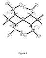
- Figure 1 is a single crystal structure of bis(N,N'-di(tert-butyl)diaminosilyl)titanium for use in the CVD or ALD of titanium silicon nitride containing films.
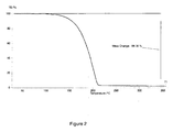
- Figure 2 is a graph of thermal gravimetric analysis (TGA) of bis(N,N'-di(tert-butyl)diaminosilyl)titanium. The almost complete weight loss indicates it is volatile and can be readily delivered into a reaction chamber in a typical CVD or ALD process. Thus, it is a suitable precursor to prepare titanium silicon nitride containing films with or without ammonia or other suitable nitrogen containing reagent.
- Figure 3 shows the deposition rate (Å/min (0.1 nm/min)) of Ti-Si-N films as a function of substrate temperature at a deposition pressure of 1.5 Torr (200 Pa) with a He carrier gas flow rate of 46 sccm (standard cubic centimetres per minute) with and without ammonia.
- Figure 4 shows the composition of titanium silicon nitride films at various temperatures. The titanium silicon nitride films are formed from chemical vapor deposition using Ti(H2Si(NBut)2)2 as organometallic precursor.
- Copper has now effectively replaced aluminum as the interconnect metal for semiconductor logic devices due to its superior electrical conductivity and high electromigration resistance. However, copper can quickly and destructively diffuse through other materials in the device such as silicon or inter-level dielectrics leading to electrical malfunctioning in the finished product. For these reasons it is necessary to encapsulate the copper with diffusion barriers. Metal nitride and metal silicon nitride thin films are candidate materials for these diffusion barriers. They can also be used close to the silicon surface of a transistor as gate electrode materials, where they pose no contamination threat to the silicon and can be processed at relatively high temperatures. Metal nitride layers, e.g., titanium nitride (TiN) layers have been employed as barrier layers against diffusion, including copper diffusion, in semiconductor device structures, e.g., contacts, vias and trenches. However, these barrier layers must be extremely thin to accommodate the higher aspect ratios of today's devices, since it is desirable for the barrier to contribute the least additional resistance to a copper interconnect as possible. These barriers must be chemically inert and must resist inter-diffusion of adjacent materials through them, have low electrical resistivity (exhibit high conductivity), low contact or via resistance and low junction leakage.
- Metal nitrides tend to be metallic compounds than can possess a crystalline structure, whereas the metal nitride/silicon nitride films tend to be amorphous. In the former case, the crystallinity of the film can provide for a breakdown of its barrier properties, since copper diffusion can occur along its crystal grain boundaries. In the latter case, since the materials are amorphous, there are no grain boundaries so barrier properties are improved. From an alternative perspective, the silicon nitride component acts to block the grain boundaries in the metal nitride.
- However, as more silicon nitride is added into the metal nitride to achieve this amorphous nature, the electrical resistivity of the material increases so the level of silicon nitride needs to be carefully controlled. Typically these barrier films need to be grown as highly conformal thin films capable of evenly coating deeply etched features on a silicon wafer with a precisely controlled film thickness. These features are ultimately filled with copper to provide the interconnecting electrical pathways between transistor devices at the silicon wafer surface. Chemical vapor deposition ("CVD") is often used to grow these conformal thin films, but as device dimensions continue to shrink barrier film thicknesses on the order of 10 Angstroms (1 nm) are needed. At this point CVD becomes challenged and atomic layer deposition ("ALD") becomes more attractive. In either case, volatile metal compounds are required as precursors. For metal nitride films, such as titanium nitride, tantalum nitride or tungsten nitride, metal amide or amide/imide compounds are used. These compounds are reacted in an ALD or CVD process with a suitable reagent, such as ammonia, to deposit a metal nitride. An example would be the CVD process, which uses the precursor tetrakis(diethylamido)titanium reacting with ammonia to give TiN. Alternatively, a precursor can be thermolysed on the wafer surface in a CVD process to give a continuous thin film of a titanium carbonitride material, which is subsequently annealed using a hydrogen/nitrogen plasma to densify the film and reduce the level of carbon to give a mostly titanium nitride film.
- An example of a suitable precursor for the latter process is tetrakis(dimethylamido)titanium. Alternatively, a tantalum nitride film can be grown in an ALD process using the precursor pentakis(dimethylamido)tantalum reacting with ammonia. Alternatively, a tungsten nitride film can be grown by ALD using the precursor (ButN=)2W(NMe2)2 reacting in alternating cycles with ammonia. If silicon nitride is to be introduced into these films, it is usually done by co-reacting the metal nitride precursor with a silicon nitride precursor, such as silane or a silicon amide compound, such as tetrakis(dimethylamido)silicon. Thus, a metal (M) containing precursor, a silicon containing precursor and a nitrogen source, such as ammonia, are co-reacted together to give the MSiN film. Thus, the degree of silicon incorporation will depend to some degree upon the ability to precisely control the metering of the silicon precursor during the process.
- Currently in the formation of ternary films, a metal amide, silane, and ammonia are sequentially deposited on the substrate via cyclic deposition, but the process poses processing issues. Silane is a pyrophoric gas and creates a potential safety hazard. In addition, three precursors are employed in the cyclic process, requiring three deposition steps along with respective purge steps. On the other hand, aminosilane or hydrazinosilane and ammonia have been reported to form silicon nitride. Importantly, though, it has been found that in these films, there is no direct metal-silicon bond in the metal silicon nitride formed by either chemical vapor deposition or atomic layer deposition, implying metal nitride and silicon nitride are in separate phases in the resulting film, i.e., metal nitride is stuffed with silicon nitride. The present invention is a potentially more elegant approach to growing MSiN films which uses a precursor that already has both the metal and silicon in its structure so both elements are delivered in the same molecule at a precisely fixed ratio, although the exact ratio of metal to silicon in a film resulting from the processing of such a precursor can still be controlled as a function of the exact process conditions of pressure, temperature, energy input and flows. The present invention will be illustrated in several non-limiting examples, set forth below.
- Under an atmosphere of dry nitrogen, 7.0g (40 mmoles) of bis(tert-butylamino)silane were dissolved in 100 ml of dry tetrahydrofuran solvent and cooled to -78°C. To this solution 32.0 ml (840 mmoles) of 2.5 M n-butyl lithium in hexanes were added dropwise over a 10 minute period and the resulting mixture stirred for an additional 30 minutes at -78°C resulting in the formation of a white precipitate. This mixture was then allowed to warm to room temperature for an additional 20 minutes after which it was re-cooled to -78°C. To a separate vessel containing 10 ml of dry tetrahydrofuran under a nitrogen atmosphere was slowly added 2.14 ml (10mmoles) of titanium tetrachloride resulting in the formation of a yellow precipitate. This latter precipitate was then added to the first precipitate at -78°C and then allowed to warm to room temperature and stir overnight. The tetrahydrofuran and hexane solvents were then stripped off under vacuum and the resulting yellow-green solid was mixed with 100 ml of fresh dry hexane under nitrogen, the resulting mixture filtered and the resulting green oil was heated to 110°C under dynamic vacuum and distilled over as an orange colored solid into a collection vessel cooled with liquid nitrogen. Yield = 3.6.g (45%). This crude product was then further purified by sublimation at 65-70°C. The structure was confirmed by single crystal X-ray analysis (see the drawing in Figure 1).
1H NMR : (500 MHz, C6D6): δ= 1.35 (s, 36H), δ= 5.41 (s, 4H).
13C NMR: (500 MHz, C6D6): δ= 35.25 (s, 12C), δ= 58.97 (s, 4C). - Mass spectrum shows a strong peak at 387m/z (ie parent of 393 m/z minus CH3 of 15 m/z).
- An alternative synthesis may also be used where two equivalents of the dianion of bis(tert-butylamino)silane are added to titanium tetrachloride in hexanes or dry tetrahydrofuran at -78°C and the resulting mixture processed as above.
- A graph of thermal gravimetric analysis (TGA) of bis(N,N'-di(tert-butyl)diaminosilyl)titanium was shown in Fig. 2. The almost complete weight loss indicated it was volatile and could be readily delivered into a reaction chamber in a typical CVD or ALD process. Thus, it is a suitable precursor to prepare titanium silicon nitride containing films with or without ammonia or other suitable nitrogen containing reagent.
- Under an atmosphere of dry nitrogen, 3.48g (20 mmoles) of bis(tert-butylamino)silane were dissolved in 100 ml of dry tetrahydrofuran solvent and cooled to -78°C. To this solution 24.4 ml (40 mmoles) of 1.6 M n-butyl lithium in hexanes were added dropwise over a 10 minute period and the resulting mixture stirred for an additional 30 minutes at -78°C resulting in the formation of a white precipitate. This mixture was then allowed to warm to room temperature for an additional 20 minutes after which it was re-cooled to -78°C. To a separate vessel containing 10 ml of dry tetrahydrofuran under a nitrogen atmosphere was slowly added 0.55 ml (5 mmoles) of titanium tetrachloride resulting in the formation of a yellow precipitate. This titanium precipitate was then added to the lithiated mixture at -78°C. To this mixture, 20g (20 mmoles) of 5 wt% lithium dimethylamide was added maintaining -78°C. The resulting mixture was then allowed to warm to room temperature and stirred overnight. The solvents were then stripped and the resulting crude product was mixed with 100 ml of dry hexane under nitrogen, filtered and the hexane then removed under vacuum. The resulting oil was then heated to 110°C under dynamic vacuum and distilled over as an orange colored solid into a collection vessel cooled with liquid nitrogen. This orange colored product was then purified by vacuum sublimation at 60°C.
- Ti(H2Si(NBut)2)2 was used as the organometallic precursor for the formation of metal silicon nitride films in a conventional CVD apparatus using known CVD techniques.
- Ti(H2Si(NBut)2)2 was vaporized in a bubbler at 90 °C and transported into a CVD chamber in combination with and without NH3 as a nitrogen-containing source. The CVD chamber was a cold-wall system having a heated substrate holder. The substrate was maintained at the temperature range from 400 to 500 °C. The chamber pressure was maintained at 1 to 2 Torr (130 to 270 Pa).
- The deposition rate of Ti-Si-N films as a function of substrate temperature at a deposition pressure of 1.5 Torr (200 Pa) with a He carrier gas flow rate of 46 sccm was shown in Figure 3. The flow rate of NH3 ranged from 0 sccm (no NH3) to 75sccm. The deposition rates increased as the substrate temperature increased. The deposition with no NH3 had the lowest deposition rate, indicating the presence of NH3 promoted the formation of titanium silicon nitride films.
- EDX analysis of titanium silicon nitride films deposited at various temperatures with NH3 as a nitrogen-containing source indicated that the films contained titanium, silicon, and nitrogen atoms (as shown in Figure 4).
Claims (28)
- An organometallic complex represented by the structure:
 each Ra is independently selected from dialkylamide, difluoralkylamide, hydrogen, alkyl, alkoxy, fluoroalkoxy, fluoroalkyl, cycloaliphatic, and aryl or two adjacent Ra can together form a ring optionally containing nitrogen or oxygen;each Rb is independently selected from dialkylamide, difluoralkylamide, hydrogen, alkyl, alkoxy, fluoroalkoxy, fluoroalkyl, cycloaliphatic, and aryl;M is a metal of Group 4, 5 or 6 of the Periodic Table of the Elements;x is at least 1 andwhen M is a Group 4 metal, 2x + y = 4,when M is a Group 5 metal, 2x + y =5, andwhen M is a Group 6 metal, 2x + y = 6.
 - An organometallic complex as claimed in Claim 1 represented by the structure:

- The organometallic complex of Claim 2, wherein one or both R1 and/or one or both R2 are hydrogen.
- The organometallic complex of Claim 2 or Claim 3, wherein one or both R3 and/or one or both R4 are t-butyl.
- The organometallic complex of Claim 2, comprising bis(N,N'-di(tert-butyl)-diaminosilyl)titanium.
- An organometallic complex as claimed in Claim 1 represented by the structure:

- The organometallic complex of Claim 6, wherein one or both R5 and/or one or both R6 are selected from hydrogen and dimethylamino.
- The organometallic complex of Claim 6 or Claim 7, wherein one or both R7 and/or one or both R8 are t-butyl.
- The organometallic complex of any one of Claims 6 to 8, wherein one or both R9 and/or one or both R10 are methyl.
- The organometallic complex of Claim 6, comprising HSi(NMe2)(ButN)2Ti(NMe2)2.
- The organometallic complex of any one of Claims 1 to 4 and 6 to 9, wherein M is selected from titanium, zirconium and hafnium.
- An organometallic complex as claimed in Claim 1 represented by the structure:

- The organometallic complex of Claim 12 wherein M is selected from vanadium, niobium, and tantalum.
- An organometallic complex as claimed in Claim 1 represented by the structure:
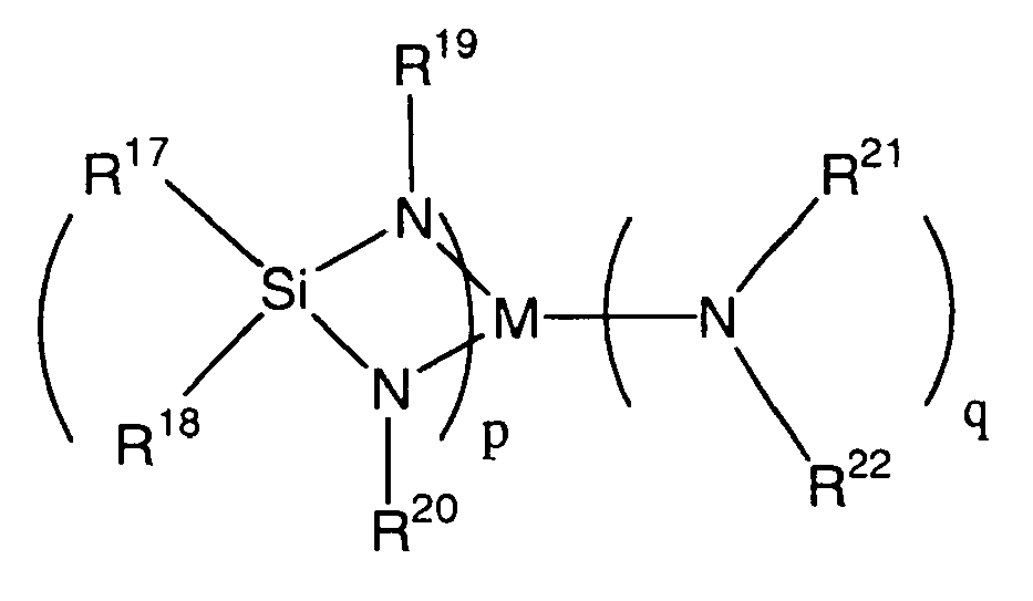
- The organometallic complex of Claim 14 wherein M is selected from chromium, molybdenum and tungsten.
- A deposition process for forming conformal metal silicon nitride thin film on a substrate wherein an organometallic complex as claimed in any one of the preceding claims is introduced to a deposition chamber, vaporized and deposited on a substrate.
- An ALD or CVD process wherein an organometallic complex as claimed in any one of Claims 1 to 15 is reacted as precursor with a nitrogen containing reagent selected from ammonia, hydrazine, dimethylhydrazine and nitrogen to form a metal silicon nitride-based film.
- An ALD or CVD process as claimed in Claim 17, wherein the reaction condition is selected from thermal, plasma, remote plasma and other energizing environment.
- An ALD or CVD process wherein an organometallic complex as claimed in any one of Claims 1 to 15 is reacted as precursor with a reagent selected from an oxidizing reagent and mixture of oxidizing and nitrogen containing reagents to form a metal silicon oxide or oxynitride-based film.
- An ALD or CVD process as claimed in Claim 19, wherein the reaction condition is selected from thermal, plasma, remote plasma and other energizing environment.
- A cyclic deposition process to form a metal silicon nitride film on a substrate comprising the steps:introducing an organometallic precursor to a deposition chamber and depositing a film on a heated substrate;purging the deposition chamber to remove unreacted organometallic precursor and any byproduct;introducing a metal amide to deposit a film on a heated substrate;purging the deposition chamber to remove any unreacted metal amide and byproduct; and,repeating the cyclic deposition process until a desired thickness of film is established.
- A process as claimed in Claim 21, wherein the metal amide is an amide of a metal selected from titanium, zirconium, hafnium, tantalum and tungsten.
- A process as claimed in Claim 20 or Claim 21, wherein the metal amide comprises one or more groups selected from dimethylamino, diethylamino, ethylmethylamino, tert-butylimino, ethylimino and tert-amylimino.
- The process of any one of Claims 21 to 23 wherein the organometallic complex is as claimed in any one of Claims 1 to 15.
- The process of any one of Claims 21 to 24 wherein the metal amide is selected from tetrakis(dimethylamino)titanium (TDMAT), tetrakis(diethylamino)titanium (TDEAT), tetrakis(ethylmethylamino)titanium (TEMAT), tetrakis(dimethylamino)zirconium (TDMAZ), tetrakis(diethylamino)zirconium (TDEAZ), tetrakis(ethylmethylamino)zirconium (TEMAZ), tetrakis(dimethylamino)hafnium (TDMAH), tetrakis(diethylamino)hafnium (TDEAH), tetrakis(ethylmethylamino)hafnium (TEMAH), tert-butylimino tris(diethylamino)tantalum (TBTDET), tert-butylimino tris(dimethylamino)tantalum (TBTDMT), tert-butylimino tris(ethylmethylamino)tantalum (TBTEMT), ethyllimino tris(diethylamino)tantalum (EITDET), ethyllimino tris(dimethylamino)tantalum (EITDMT), ethyllimino tris(ethylmethylamino)tantalum (EITEMT), tert-amylimino tris(dimethylamino)tantalum (TAIMAT), tert-amylimino tris(diethylamino)tantalum, pentakis(dimethylamino)tantalum, tert-amylimino tri(ethylmethylamino)tantalum, bis(tert-butylimino)bis(dimethylamino)tungsten (BTBMW), bis(tert-butylimino)bis(diethylamino)tungsten, bis(tert-butylimino)bis(ethylmethylamino)tungsten, and a mixture thereof.
- The deposition process of any one of Claims 16 to 25 selected from an atomic layer deposition (ALD) process and a chemical vapor deposition (CVD) process, optionally with ammonia.
- The process of any one of Claims 16 to 26 using an additional treatment step selected for final film densification or film annealing, selected from thermal, ozone, plasma, UV and microwave.
- An CVD process optionally with ammonia employing a mixture comprising(A)a precursor consisting of an organometallic complex as claimed in any one of Claims 1 to 15(B)a metal amide selected from tetrakis(dimethylamino)titanium (TDMAT), tetrakis(diethylamino)titanium (TDEAT), tetrakis(ethylmethylamino)titanium (TEMAT), tetrakis(dimethylamino)zirconium (TDMAZ), tetrakis(diethylamino)zirconium (TDEAZ), tetrakis(ethylmethylamino)zirconium (TEMAZ), tetrakis(dimethylamino)hafnium (TDMAH), tetrakis(diethylamino)hafnium (TDEAH), tetrakis(ethylmethylamino)hafnium (TEMAH), tert-butylimino tris(diethylamino)tantalum (TBTDET), tert-butylimino tris(dimethylamino)tantalum (TBTDMT), tert-butylimino tris(ethylmethylamino)tantalum (TBTEMT), ethyllimino tris(diethylamino)tantalum (EITDET), ethyllimino tris(dimethylamino)tantalum (EITDMT), ethyllimino tris(ethylmethylamino)tantalum (EITEMT), tert-amylimino tris(dimethylamino)tantalum (TAIMAT), tert-amylimino tris(diethylamino)tantalum, pentakis(dimethylamino)tantalum, tert-amylimino tri(ethylmethylamino)tantalum, bis(tert-butylimino)bis(dimethylamino)tungsten (BTBMW), bis(tert-butylimino)bis(diethylamino)tungsten, bis(tert-butylimino)bis(ethylmethylamino)tungsten, and a mixture thereof.
Applications Claiming Priority (2)
| Application Number | Priority Date | Filing Date | Title |
|---|---|---|---|
| US72475705P | 2005-10-07 | 2005-10-07 | |
| US11/522,768 US7754906B2 (en) | 2005-10-07 | 2006-09-18 | Ti, Ta, Hf, Zr and related metal silicon amides for ALD/CVD of metal-silicon nitrides, oxides or oxynitrides |
Publications (2)
| Publication Number | Publication Date |
|---|---|
| EP1772460A1 true EP1772460A1 (en) | 2007-04-11 |
| EP1772460B1 EP1772460B1 (en) | 2009-03-25 |
Family
ID=37603419
Family Applications (1)
| Application Number | Title | Priority Date | Filing Date |
|---|---|---|---|
| EP06255104A Not-in-force EP1772460B1 (en) | 2005-10-07 | 2006-10-03 | Ti, Ta, Hf, Zr and related metal silicon amides for ALD/CVD of metal-silicon nitrides, oxides, oxides or oxynitrides |
Country Status (8)
| Country | Link |
|---|---|
| US (1) | US7754906B2 (en) |
| EP (1) | EP1772460B1 (en) |
| JP (2) | JP4555272B2 (en) |
| KR (1) | KR100862263B1 (en) |
| CN (1) | CN1990492B (en) |
| AT (1) | ATE426606T1 (en) |
| DE (1) | DE602006005877D1 (en) |
| TW (1) | TWI336732B (en) |
Cited By (1)
| Publication number | Priority date | Publication date | Assignee | Title |
|---|---|---|---|---|
| US20220127724A1 (en) * | 2020-10-22 | 2022-04-28 | Asm Ip Holding B.V. | Method of depositing vanadium metal, structure, device and a deposition assembly |
Families Citing this family (379)
| Publication number | Priority date | Publication date | Assignee | Title |
|---|---|---|---|---|
| DE102005033579A1 (en) * | 2005-07-19 | 2007-01-25 | H.C. Starck Gmbh | Process for the preparation of thin hafnium or zirconium nitride layers |
| US7678422B2 (en) * | 2006-12-13 | 2010-03-16 | Air Products And Chemicals, Inc. | Cyclic chemical vapor deposition of metal-silicon containing films |
| KR100956210B1 (en) * | 2007-06-19 | 2010-05-04 | 에어 프로덕츠 앤드 케미칼스, 인코오포레이티드 | Plasma Enhanced Cyclic Deposition of Metal Silicon Nitride Thin Films |
| US7858144B2 (en) * | 2007-09-26 | 2010-12-28 | Eastman Kodak Company | Process for depositing organic materials |
| US20100037820A1 (en) * | 2008-08-13 | 2010-02-18 | Synos Technology, Inc. | Vapor Deposition Reactor |
| US20100037824A1 (en) * | 2008-08-13 | 2010-02-18 | Synos Technology, Inc. | Plasma Reactor Having Injector |
| US8770142B2 (en) | 2008-09-17 | 2014-07-08 | Veeco Ald Inc. | Electrode for generating plasma and plasma generator |
| US8851012B2 (en) | 2008-09-17 | 2014-10-07 | Veeco Ald Inc. | Vapor deposition reactor using plasma and method for forming thin film using the same |
| US10378106B2 (en) | 2008-11-14 | 2019-08-13 | Asm Ip Holding B.V. | Method of forming insulation film by modified PEALD |
| WO2010067778A1 (en) * | 2008-12-09 | 2010-06-17 | 株式会社アルバック | Tantalum nitride film formation method and film formation device therefore |
| US8871628B2 (en) * | 2009-01-21 | 2014-10-28 | Veeco Ald Inc. | Electrode structure, device comprising the same and method for forming electrode structure |
| US8257799B2 (en) | 2009-02-23 | 2012-09-04 | Synos Technology, Inc. | Method for forming thin film using radicals generated by plasma |
| US9394608B2 (en) | 2009-04-06 | 2016-07-19 | Asm America, Inc. | Semiconductor processing reactor and components thereof |
| US8758512B2 (en) * | 2009-06-08 | 2014-06-24 | Veeco Ald Inc. | Vapor deposition reactor and method for forming thin film |
| US8802201B2 (en) | 2009-08-14 | 2014-08-12 | Asm America, Inc. | Systems and methods for thin-film deposition of metal oxides using excited nitrogen-oxygen species |
| US8771791B2 (en) | 2010-10-18 | 2014-07-08 | Veeco Ald Inc. | Deposition of layer using depositing apparatus with reciprocating susceptor |
| US8877300B2 (en) * | 2011-02-16 | 2014-11-04 | Veeco Ald Inc. | Atomic layer deposition using radicals of gas mixture |
| US9163310B2 (en) | 2011-02-18 | 2015-10-20 | Veeco Ald Inc. | Enhanced deposition of layer on substrate using radicals |
| US9312155B2 (en) | 2011-06-06 | 2016-04-12 | Asm Japan K.K. | High-throughput semiconductor-processing apparatus equipped with multiple dual-chamber modules |
| US10364496B2 (en) | 2011-06-27 | 2019-07-30 | Asm Ip Holding B.V. | Dual section module having shared and unshared mass flow controllers |
| US10854498B2 (en) | 2011-07-15 | 2020-12-01 | Asm Ip Holding B.V. | Wafer-supporting device and method for producing same |
| US20130023129A1 (en) | 2011-07-20 | 2013-01-24 | Asm America, Inc. | Pressure transmitter for a semiconductor processing environment |
| US9017481B1 (en) | 2011-10-28 | 2015-04-28 | Asm America, Inc. | Process feed management for semiconductor substrate processing |
| US9659799B2 (en) | 2012-08-28 | 2017-05-23 | Asm Ip Holding B.V. | Systems and methods for dynamic semiconductor process scheduling |
| US10714315B2 (en) | 2012-10-12 | 2020-07-14 | Asm Ip Holdings B.V. | Semiconductor reaction chamber showerhead |
| US20160376700A1 (en) | 2013-02-01 | 2016-12-29 | Asm Ip Holding B.V. | System for treatment of deposition reactor |
| US9589770B2 (en) | 2013-03-08 | 2017-03-07 | Asm Ip Holding B.V. | Method and systems for in-situ formation of intermediate reactive species |
| US9484191B2 (en) | 2013-03-08 | 2016-11-01 | Asm Ip Holding B.V. | Pulsed remote plasma method and system |
| EP3366808B1 (en) * | 2013-06-28 | 2023-10-25 | Wayne State University | Method of forming layers on a substrate |
| US9249505B2 (en) | 2013-06-28 | 2016-02-02 | Wayne State University | Bis(trimethylsilyl) six-membered ring systems and related compounds as reducing agents for forming layers on a substrate |
| US9240412B2 (en) | 2013-09-27 | 2016-01-19 | Asm Ip Holding B.V. | Semiconductor structure and device and methods of forming same using selective epitaxial process |
| US10683571B2 (en) | 2014-02-25 | 2020-06-16 | Asm Ip Holding B.V. | Gas supply manifold and method of supplying gases to chamber using same |
| US10167557B2 (en) | 2014-03-18 | 2019-01-01 | Asm Ip Holding B.V. | Gas distribution system, reactor including the system, and methods of using the same |
| US11015245B2 (en) | 2014-03-19 | 2021-05-25 | Asm Ip Holding B.V. | Gas-phase reactor and system having exhaust plenum and components thereof |
| US10858737B2 (en) | 2014-07-28 | 2020-12-08 | Asm Ip Holding B.V. | Showerhead assembly and components thereof |
| US9890456B2 (en) | 2014-08-21 | 2018-02-13 | Asm Ip Holding B.V. | Method and system for in situ formation of gas-phase compounds |
| US10941490B2 (en) | 2014-10-07 | 2021-03-09 | Asm Ip Holding B.V. | Multiple temperature range susceptor, assembly, reactor and system including the susceptor, and methods of using the same |
| US9657845B2 (en) | 2014-10-07 | 2017-05-23 | Asm Ip Holding B.V. | Variable conductance gas distribution apparatus and method |
| KR102263121B1 (en) | 2014-12-22 | 2021-06-09 | 에이에스엠 아이피 홀딩 비.브이. | Semiconductor device and manufacuring method thereof |
| US10529542B2 (en) | 2015-03-11 | 2020-01-07 | Asm Ip Holdings B.V. | Cross-flow reactor and method |
| US10276355B2 (en) | 2015-03-12 | 2019-04-30 | Asm Ip Holding B.V. | Multi-zone reactor, system including the reactor, and method of using the same |
| US10458018B2 (en) | 2015-06-26 | 2019-10-29 | Asm Ip Holding B.V. | Structures including metal carbide material, devices including the structures, and methods of forming same |
| US10600673B2 (en) | 2015-07-07 | 2020-03-24 | Asm Ip Holding B.V. | Magnetic susceptor to baseplate seal |
| US10083836B2 (en) | 2015-07-24 | 2018-09-25 | Asm Ip Holding B.V. | Formation of boron-doped titanium metal films with high work function |
| US9960072B2 (en) | 2015-09-29 | 2018-05-01 | Asm Ip Holding B.V. | Variable adjustment for precise matching of multiple chamber cavity housings |
| US10211308B2 (en) | 2015-10-21 | 2019-02-19 | Asm Ip Holding B.V. | NbMC layers |
| US10322384B2 (en) | 2015-11-09 | 2019-06-18 | Asm Ip Holding B.V. | Counter flow mixer for process chamber |
| US11139308B2 (en) | 2015-12-29 | 2021-10-05 | Asm Ip Holding B.V. | Atomic layer deposition of III-V compounds to form V-NAND devices |
| US10529554B2 (en) | 2016-02-19 | 2020-01-07 | Asm Ip Holding B.V. | Method for forming silicon nitride film selectively on sidewalls or flat surfaces of trenches |
| US10468251B2 (en) | 2016-02-19 | 2019-11-05 | Asm Ip Holding B.V. | Method for forming spacers using silicon nitride film for spacer-defined multiple patterning |
| US10501866B2 (en) | 2016-03-09 | 2019-12-10 | Asm Ip Holding B.V. | Gas distribution apparatus for improved film uniformity in an epitaxial system |
| US10343920B2 (en) | 2016-03-18 | 2019-07-09 | Asm Ip Holding B.V. | Aligned carbon nanotubes |
| US9892913B2 (en) | 2016-03-24 | 2018-02-13 | Asm Ip Holding B.V. | Radial and thickness control via biased multi-port injection settings |
| US10865475B2 (en) | 2016-04-21 | 2020-12-15 | Asm Ip Holding B.V. | Deposition of metal borides and silicides |
| US10190213B2 (en) | 2016-04-21 | 2019-01-29 | Asm Ip Holding B.V. | Deposition of metal borides |
| US10367080B2 (en) | 2016-05-02 | 2019-07-30 | Asm Ip Holding B.V. | Method of forming a germanium oxynitride film |
| US10032628B2 (en) | 2016-05-02 | 2018-07-24 | Asm Ip Holding B.V. | Source/drain performance through conformal solid state doping |
| KR102592471B1 (en) | 2016-05-17 | 2023-10-20 | 에이에스엠 아이피 홀딩 비.브이. | Method of forming metal interconnection and method of fabricating semiconductor device using the same |
| US11453943B2 (en) | 2016-05-25 | 2022-09-27 | Asm Ip Holding B.V. | Method for forming carbon-containing silicon/metal oxide or nitride film by ALD using silicon precursor and hydrocarbon precursor |
| US10388509B2 (en) | 2016-06-28 | 2019-08-20 | Asm Ip Holding B.V. | Formation of epitaxial layers via dislocation filtering |
| US9859151B1 (en) | 2016-07-08 | 2018-01-02 | Asm Ip Holding B.V. | Selective film deposition method to form air gaps |
| US10612137B2 (en) | 2016-07-08 | 2020-04-07 | Asm Ip Holdings B.V. | Organic reactants for atomic layer deposition |
| US10714385B2 (en) | 2016-07-19 | 2020-07-14 | Asm Ip Holding B.V. | Selective deposition of tungsten |
| KR102354490B1 (en) | 2016-07-27 | 2022-01-21 | 에이에스엠 아이피 홀딩 비.브이. | Method of processing a substrate |
| US9887082B1 (en) | 2016-07-28 | 2018-02-06 | Asm Ip Holding B.V. | Method and apparatus for filling a gap |
| KR102532607B1 (en) | 2016-07-28 | 2023-05-15 | 에이에스엠 아이피 홀딩 비.브이. | Substrate processing apparatus and method of operating the same |
| US9812320B1 (en) | 2016-07-28 | 2017-11-07 | Asm Ip Holding B.V. | Method and apparatus for filling a gap |
| US10395919B2 (en) | 2016-07-28 | 2019-08-27 | Asm Ip Holding B.V. | Method and apparatus for filling a gap |
| US10410943B2 (en) | 2016-10-13 | 2019-09-10 | Asm Ip Holding B.V. | Method for passivating a surface of a semiconductor and related systems |
| CN106544001B (en) * | 2016-10-21 | 2019-12-31 | 河南大学 | A kind of guar gum fracturing fluid nano-crosslinking agent with good temperature resistance and preparation method thereof |
| US10643826B2 (en) | 2016-10-26 | 2020-05-05 | Asm Ip Holdings B.V. | Methods for thermally calibrating reaction chambers |
| US11532757B2 (en) | 2016-10-27 | 2022-12-20 | Asm Ip Holding B.V. | Deposition of charge trapping layers |
| US10714350B2 (en) | 2016-11-01 | 2020-07-14 | ASM IP Holdings, B.V. | Methods for forming a transition metal niobium nitride film on a substrate by atomic layer deposition and related semiconductor device structures |
| US10435790B2 (en) | 2016-11-01 | 2019-10-08 | Asm Ip Holding B.V. | Method of subatmospheric plasma-enhanced ALD using capacitively coupled electrodes with narrow gap |
| US10643904B2 (en) | 2016-11-01 | 2020-05-05 | Asm Ip Holdings B.V. | Methods for forming a semiconductor device and related semiconductor device structures |
| US10229833B2 (en) | 2016-11-01 | 2019-03-12 | Asm Ip Holding B.V. | Methods for forming a transition metal nitride film on a substrate by atomic layer deposition and related semiconductor device structures |
| US10134757B2 (en) | 2016-11-07 | 2018-11-20 | Asm Ip Holding B.V. | Method of processing a substrate and a device manufactured by using the method |
| KR102546317B1 (en) | 2016-11-15 | 2023-06-21 | 에이에스엠 아이피 홀딩 비.브이. | Gas supply unit and substrate processing apparatus including the same |
| US10340135B2 (en) | 2016-11-28 | 2019-07-02 | Asm Ip Holding B.V. | Method of topologically restricted plasma-enhanced cyclic deposition of silicon or metal nitride |
| KR102762543B1 (en) | 2016-12-14 | 2025-02-05 | 에이에스엠 아이피 홀딩 비.브이. | Substrate processing apparatus |
| US11581186B2 (en) | 2016-12-15 | 2023-02-14 | Asm Ip Holding B.V. | Sequential infiltration synthesis apparatus |
| US11447861B2 (en) | 2016-12-15 | 2022-09-20 | Asm Ip Holding B.V. | Sequential infiltration synthesis apparatus and a method of forming a patterned structure |
| KR102700194B1 (en) | 2016-12-19 | 2024-08-28 | 에이에스엠 아이피 홀딩 비.브이. | Substrate processing apparatus |
| US10269558B2 (en) | 2016-12-22 | 2019-04-23 | Asm Ip Holding B.V. | Method of forming a structure on a substrate |
| US10867788B2 (en) | 2016-12-28 | 2020-12-15 | Asm Ip Holding B.V. | Method of forming a structure on a substrate |
| US11390950B2 (en) | 2017-01-10 | 2022-07-19 | Asm Ip Holding B.V. | Reactor system and method to reduce residue buildup during a film deposition process |
| US10655221B2 (en) | 2017-02-09 | 2020-05-19 | Asm Ip Holding B.V. | Method for depositing oxide film by thermal ALD and PEALD |
| US10468261B2 (en) | 2017-02-15 | 2019-11-05 | Asm Ip Holding B.V. | Methods for forming a metallic film on a substrate by cyclical deposition and related semiconductor device structures |
| US10529563B2 (en) | 2017-03-29 | 2020-01-07 | Asm Ip Holdings B.V. | Method for forming doped metal oxide films on a substrate by cyclical deposition and related semiconductor device structures |
| US10283353B2 (en) | 2017-03-29 | 2019-05-07 | Asm Ip Holding B.V. | Method of reforming insulating film deposited on substrate with recess pattern |
| US10103040B1 (en) | 2017-03-31 | 2018-10-16 | Asm Ip Holding B.V. | Apparatus and method for manufacturing a semiconductor device |
| KR102457289B1 (en) | 2017-04-25 | 2022-10-21 | 에이에스엠 아이피 홀딩 비.브이. | Method for depositing a thin film and manufacturing a semiconductor device |
| US10446393B2 (en) | 2017-05-08 | 2019-10-15 | Asm Ip Holding B.V. | Methods for forming silicon-containing epitaxial layers and related semiconductor device structures |
| US10892156B2 (en) | 2017-05-08 | 2021-01-12 | Asm Ip Holding B.V. | Methods for forming a silicon nitride film on a substrate and related semiconductor device structures |
| US10770286B2 (en) | 2017-05-08 | 2020-09-08 | Asm Ip Holdings B.V. | Methods for selectively forming a silicon nitride film on a substrate and related semiconductor device structures |
| US10504742B2 (en) | 2017-05-31 | 2019-12-10 | Asm Ip Holding B.V. | Method of atomic layer etching using hydrogen plasma |
| US10886123B2 (en) | 2017-06-02 | 2021-01-05 | Asm Ip Holding B.V. | Methods for forming low temperature semiconductor layers and related semiconductor device structures |
| US12040200B2 (en) | 2017-06-20 | 2024-07-16 | Asm Ip Holding B.V. | Semiconductor processing apparatus and methods for calibrating a semiconductor processing apparatus |
| US11306395B2 (en) | 2017-06-28 | 2022-04-19 | Asm Ip Holding B.V. | Methods for depositing a transition metal nitride film on a substrate by atomic layer deposition and related deposition apparatus |
| US10685834B2 (en) | 2017-07-05 | 2020-06-16 | Asm Ip Holdings B.V. | Methods for forming a silicon germanium tin layer and related semiconductor device structures |
| KR20190009245A (en) | 2017-07-18 | 2019-01-28 | 에이에스엠 아이피 홀딩 비.브이. | Methods for forming a semiconductor device structure and related semiconductor device structures |
| US11018002B2 (en) | 2017-07-19 | 2021-05-25 | Asm Ip Holding B.V. | Method for selectively depositing a Group IV semiconductor and related semiconductor device structures |
| US10541333B2 (en) | 2017-07-19 | 2020-01-21 | Asm Ip Holding B.V. | Method for depositing a group IV semiconductor and related semiconductor device structures |
| US11374112B2 (en) | 2017-07-19 | 2022-06-28 | Asm Ip Holding B.V. | Method for depositing a group IV semiconductor and related semiconductor device structures |
| US10590535B2 (en) | 2017-07-26 | 2020-03-17 | Asm Ip Holdings B.V. | Chemical treatment, deposition and/or infiltration apparatus and method for using the same |
| US10605530B2 (en) | 2017-07-26 | 2020-03-31 | Asm Ip Holding B.V. | Assembly of a liner and a flange for a vertical furnace as well as the liner and the vertical furnace |
| US10312055B2 (en) | 2017-07-26 | 2019-06-04 | Asm Ip Holding B.V. | Method of depositing film by PEALD using negative bias |
| TWI815813B (en) | 2017-08-04 | 2023-09-21 | 荷蘭商Asm智慧財產控股公司 | Showerhead assembly for distributing a gas within a reaction chamber |
| US10770336B2 (en) | 2017-08-08 | 2020-09-08 | Asm Ip Holding B.V. | Substrate lift mechanism and reactor including same |
| US10692741B2 (en) | 2017-08-08 | 2020-06-23 | Asm Ip Holdings B.V. | Radiation shield |
| US11769682B2 (en) | 2017-08-09 | 2023-09-26 | Asm Ip Holding B.V. | Storage apparatus for storing cassettes for substrates and processing apparatus equipped therewith |
| US11139191B2 (en) | 2017-08-09 | 2021-10-05 | Asm Ip Holding B.V. | Storage apparatus for storing cassettes for substrates and processing apparatus equipped therewith |
| US10249524B2 (en) | 2017-08-09 | 2019-04-02 | Asm Ip Holding B.V. | Cassette holder assembly for a substrate cassette and holding member for use in such assembly |
| USD900036S1 (en) | 2017-08-24 | 2020-10-27 | Asm Ip Holding B.V. | Heater electrical connector and adapter |
| US11830730B2 (en) | 2017-08-29 | 2023-11-28 | Asm Ip Holding B.V. | Layer forming method and apparatus |
| KR102491945B1 (en) | 2017-08-30 | 2023-01-26 | 에이에스엠 아이피 홀딩 비.브이. | Substrate processing apparatus |
| US11056344B2 (en) | 2017-08-30 | 2021-07-06 | Asm Ip Holding B.V. | Layer forming method |
| US11295980B2 (en) | 2017-08-30 | 2022-04-05 | Asm Ip Holding B.V. | Methods for depositing a molybdenum metal film over a dielectric surface of a substrate by a cyclical deposition process and related semiconductor device structures |
| KR102401446B1 (en) | 2017-08-31 | 2022-05-24 | 에이에스엠 아이피 홀딩 비.브이. | Substrate processing apparatus |
| CN111295465B (en) * | 2017-09-14 | 2022-12-09 | 弗萨姆材料美国有限责任公司 | Compositions and methods for depositing silicon-containing films |
| US10607895B2 (en) | 2017-09-18 | 2020-03-31 | Asm Ip Holdings B.V. | Method for forming a semiconductor device structure comprising a gate fill metal |
| KR102630301B1 (en) | 2017-09-21 | 2024-01-29 | 에이에스엠 아이피 홀딩 비.브이. | Method of sequential infiltration synthesis treatment of infiltrateable material and structures and devices formed using same |
| US10844484B2 (en) | 2017-09-22 | 2020-11-24 | Asm Ip Holding B.V. | Apparatus for dispensing a vapor phase reactant to a reaction chamber and related methods |
| US10658205B2 (en) | 2017-09-28 | 2020-05-19 | Asm Ip Holdings B.V. | Chemical dispensing apparatus and methods for dispensing a chemical to a reaction chamber |
| US10403504B2 (en) | 2017-10-05 | 2019-09-03 | Asm Ip Holding B.V. | Method for selectively depositing a metallic film on a substrate |
| US10319588B2 (en) | 2017-10-10 | 2019-06-11 | Asm Ip Holding B.V. | Method for depositing a metal chalcogenide on a substrate by cyclical deposition |
| US10923344B2 (en) | 2017-10-30 | 2021-02-16 | Asm Ip Holding B.V. | Methods for forming a semiconductor structure and related semiconductor structures |
| KR102443047B1 (en) | 2017-11-16 | 2022-09-14 | 에이에스엠 아이피 홀딩 비.브이. | Substrate processing apparatus method and apparatus manufactured thereby |
| US10910262B2 (en) | 2017-11-16 | 2021-02-02 | Asm Ip Holding B.V. | Method of selectively depositing a capping layer structure on a semiconductor device structure |
| US11022879B2 (en) | 2017-11-24 | 2021-06-01 | Asm Ip Holding B.V. | Method of forming an enhanced unexposed photoresist layer |
| JP7206265B2 (en) | 2017-11-27 | 2023-01-17 | エーエスエム アイピー ホールディング ビー.ブイ. | Equipment with a clean mini-environment |
| CN111316417B (en) | 2017-11-27 | 2023-12-22 | 阿斯莫Ip控股公司 | Storage device for use with batch furnaces for storing wafer cassettes |
| US10290508B1 (en) | 2017-12-05 | 2019-05-14 | Asm Ip Holding B.V. | Method for forming vertical spacers for spacer-defined patterning |
| US10872771B2 (en) | 2018-01-16 | 2020-12-22 | Asm Ip Holding B. V. | Method for depositing a material film on a substrate within a reaction chamber by a cyclical deposition process and related device structures |
| CN111630203A (en) | 2018-01-19 | 2020-09-04 | Asm Ip私人控股有限公司 | Method of depositing a gap fill layer by plasma assisted deposition |
| TWI799494B (en) | 2018-01-19 | 2023-04-21 | 荷蘭商Asm 智慧財產控股公司 | Deposition method |
| USD903477S1 (en) | 2018-01-24 | 2020-12-01 | Asm Ip Holdings B.V. | Metal clamp |
| US11018047B2 (en) | 2018-01-25 | 2021-05-25 | Asm Ip Holding B.V. | Hybrid lift pin |
| US10535516B2 (en) | 2018-02-01 | 2020-01-14 | Asm Ip Holdings B.V. | Method for depositing a semiconductor structure on a surface of a substrate and related semiconductor structures |
| USD880437S1 (en) | 2018-02-01 | 2020-04-07 | Asm Ip Holding B.V. | Gas supply plate for semiconductor manufacturing apparatus |
| US11081345B2 (en) | 2018-02-06 | 2021-08-03 | Asm Ip Holding B.V. | Method of post-deposition treatment for silicon oxide film |
| JP7124098B2 (en) | 2018-02-14 | 2022-08-23 | エーエスエム・アイピー・ホールディング・ベー・フェー | Method for depositing a ruthenium-containing film on a substrate by a cyclical deposition process |
| US10896820B2 (en) | 2018-02-14 | 2021-01-19 | Asm Ip Holding B.V. | Method for depositing a ruthenium-containing film on a substrate by a cyclical deposition process |
| US10731249B2 (en) | 2018-02-15 | 2020-08-04 | Asm Ip Holding B.V. | Method of forming a transition metal containing film on a substrate by a cyclical deposition process, a method for supplying a transition metal halide compound to a reaction chamber, and related vapor deposition apparatus |
| KR102636427B1 (en) | 2018-02-20 | 2024-02-13 | 에이에스엠 아이피 홀딩 비.브이. | Substrate processing method and apparatus |
| US10658181B2 (en) | 2018-02-20 | 2020-05-19 | Asm Ip Holding B.V. | Method of spacer-defined direct patterning in semiconductor fabrication |
| US10975470B2 (en) | 2018-02-23 | 2021-04-13 | Asm Ip Holding B.V. | Apparatus for detecting or monitoring for a chemical precursor in a high temperature environment |
| US11473195B2 (en) | 2018-03-01 | 2022-10-18 | Asm Ip Holding B.V. | Semiconductor processing apparatus and a method for processing a substrate |
| US11629406B2 (en) | 2018-03-09 | 2023-04-18 | Asm Ip Holding B.V. | Semiconductor processing apparatus comprising one or more pyrometers for measuring a temperature of a substrate during transfer of the substrate |
| US11114283B2 (en) | 2018-03-16 | 2021-09-07 | Asm Ip Holding B.V. | Reactor, system including the reactor, and methods of manufacturing and using same |
| KR102646467B1 (en) | 2018-03-27 | 2024-03-11 | 에이에스엠 아이피 홀딩 비.브이. | Method of forming an electrode on a substrate and a semiconductor device structure including an electrode |
| US11230766B2 (en) | 2018-03-29 | 2022-01-25 | Asm Ip Holding B.V. | Substrate processing apparatus and method |
| US10510536B2 (en) | 2018-03-29 | 2019-12-17 | Asm Ip Holding B.V. | Method of depositing a co-doped polysilicon film on a surface of a substrate within a reaction chamber |
| US11088002B2 (en) | 2018-03-29 | 2021-08-10 | Asm Ip Holding B.V. | Substrate rack and a substrate processing system and method |
| KR102501472B1 (en) | 2018-03-30 | 2023-02-20 | 에이에스엠 아이피 홀딩 비.브이. | Substrate processing method |
| KR102600229B1 (en) | 2018-04-09 | 2023-11-10 | 에이에스엠 아이피 홀딩 비.브이. | Substrate supporting device, substrate processing apparatus including the same and substrate processing method |
| US12025484B2 (en) | 2018-05-08 | 2024-07-02 | Asm Ip Holding B.V. | Thin film forming method |
| KR102709511B1 (en) | 2018-05-08 | 2024-09-24 | 에이에스엠 아이피 홀딩 비.브이. | Methods for depositing an oxide film on a substrate by a cyclical deposition process and related device structures |
| US12272527B2 (en) | 2018-05-09 | 2025-04-08 | Asm Ip Holding B.V. | Apparatus for use with hydrogen radicals and method of using same |
| TWI816783B (en) | 2018-05-11 | 2023-10-01 | 荷蘭商Asm 智慧財產控股公司 | Methods for forming a doped metal carbide film on a substrate and related semiconductor device structures |
| KR102596988B1 (en) | 2018-05-28 | 2023-10-31 | 에이에스엠 아이피 홀딩 비.브이. | Method of processing a substrate and a device manufactured by the same |
| US11718913B2 (en) | 2018-06-04 | 2023-08-08 | Asm Ip Holding B.V. | Gas distribution system and reactor system including same |
| TWI840362B (en) | 2018-06-04 | 2024-05-01 | 荷蘭商Asm Ip私人控股有限公司 | Wafer handling chamber with moisture reduction |
| US11286562B2 (en) | 2018-06-08 | 2022-03-29 | Asm Ip Holding B.V. | Gas-phase chemical reactor and method of using same |
| KR102568797B1 (en) | 2018-06-21 | 2023-08-21 | 에이에스엠 아이피 홀딩 비.브이. | Substrate processing system |
| US10797133B2 (en) | 2018-06-21 | 2020-10-06 | Asm Ip Holding B.V. | Method for depositing a phosphorus doped silicon arsenide film and related semiconductor device structures |
| KR20250134000A (en) | 2018-06-27 | 2025-09-09 | 에이에스엠 아이피 홀딩 비.브이. | Cyclic deposition methods for forming metal-containing material and films and structures including the metal-containing material |
| US11499222B2 (en) | 2018-06-27 | 2022-11-15 | Asm Ip Holding B.V. | Cyclic deposition methods for forming metal-containing material and films and structures including the metal-containing material |
| KR102686758B1 (en) | 2018-06-29 | 2024-07-18 | 에이에스엠 아이피 홀딩 비.브이. | Method for depositing a thin film and manufacturing a semiconductor device |
| US10612136B2 (en) | 2018-06-29 | 2020-04-07 | ASM IP Holding, B.V. | Temperature-controlled flange and reactor system including same |
| US10388513B1 (en) | 2018-07-03 | 2019-08-20 | Asm Ip Holding B.V. | Method for depositing silicon-free carbon-containing film as gap-fill layer by pulse plasma-assisted deposition |
| US10755922B2 (en) | 2018-07-03 | 2020-08-25 | Asm Ip Holding B.V. | Method for depositing silicon-free carbon-containing film as gap-fill layer by pulse plasma-assisted deposition |
| US10767789B2 (en) | 2018-07-16 | 2020-09-08 | Asm Ip Holding B.V. | Diaphragm valves, valve components, and methods for forming valve components |
| US10483099B1 (en) | 2018-07-26 | 2019-11-19 | Asm Ip Holding B.V. | Method for forming thermally stable organosilicon polymer film |
| US11053591B2 (en) | 2018-08-06 | 2021-07-06 | Asm Ip Holding B.V. | Multi-port gas injection system and reactor system including same |
| US10883175B2 (en) | 2018-08-09 | 2021-01-05 | Asm Ip Holding B.V. | Vertical furnace for processing substrates and a liner for use therein |
| US10829852B2 (en) | 2018-08-16 | 2020-11-10 | Asm Ip Holding B.V. | Gas distribution device for a wafer processing apparatus |
| US11430674B2 (en) | 2018-08-22 | 2022-08-30 | Asm Ip Holding B.V. | Sensor array, apparatus for dispensing a vapor phase reactant to a reaction chamber and related methods |
| US11024523B2 (en) | 2018-09-11 | 2021-06-01 | Asm Ip Holding B.V. | Substrate processing apparatus and method |
| KR102707956B1 (en) | 2018-09-11 | 2024-09-19 | 에이에스엠 아이피 홀딩 비.브이. | Method for deposition of a thin film |
| US11049751B2 (en) | 2018-09-14 | 2021-06-29 | Asm Ip Holding B.V. | Cassette supply system to store and handle cassettes and processing apparatus equipped therewith |
| CN110970344B (en) | 2018-10-01 | 2024-10-25 | Asmip控股有限公司 | Substrate holding device, system including the same and method of using the same |
| US11232963B2 (en) | 2018-10-03 | 2022-01-25 | Asm Ip Holding B.V. | Substrate processing apparatus and method |
| KR102592699B1 (en) | 2018-10-08 | 2023-10-23 | 에이에스엠 아이피 홀딩 비.브이. | Substrate support unit and apparatuses for depositing thin film and processing the substrate including the same |
| US10847365B2 (en) | 2018-10-11 | 2020-11-24 | Asm Ip Holding B.V. | Method of forming conformal silicon carbide film by cyclic CVD |
| US10811256B2 (en) | 2018-10-16 | 2020-10-20 | Asm Ip Holding B.V. | Method for etching a carbon-containing feature |
| KR102546322B1 (en) | 2018-10-19 | 2023-06-21 | 에이에스엠 아이피 홀딩 비.브이. | Substrate processing apparatus and substrate processing method |
| KR102605121B1 (en) | 2018-10-19 | 2023-11-23 | 에이에스엠 아이피 홀딩 비.브이. | Substrate processing apparatus and substrate processing method |
| USD948463S1 (en) | 2018-10-24 | 2022-04-12 | Asm Ip Holding B.V. | Susceptor for semiconductor substrate supporting apparatus |
| US10381219B1 (en) | 2018-10-25 | 2019-08-13 | Asm Ip Holding B.V. | Methods for forming a silicon nitride film |
| US12378665B2 (en) | 2018-10-26 | 2025-08-05 | Asm Ip Holding B.V. | High temperature coatings for a preclean and etch apparatus and related methods |
| US11087997B2 (en) | 2018-10-31 | 2021-08-10 | Asm Ip Holding B.V. | Substrate processing apparatus for processing substrates |
| KR102748291B1 (en) | 2018-11-02 | 2024-12-31 | 에이에스엠 아이피 홀딩 비.브이. | Substrate support unit and substrate processing apparatus including the same |
| US11572620B2 (en) | 2018-11-06 | 2023-02-07 | Asm Ip Holding B.V. | Methods for selectively depositing an amorphous silicon film on a substrate |
| US11031242B2 (en) | 2018-11-07 | 2021-06-08 | Asm Ip Holding B.V. | Methods for depositing a boron doped silicon germanium film |
| US10847366B2 (en) | 2018-11-16 | 2020-11-24 | Asm Ip Holding B.V. | Methods for depositing a transition metal chalcogenide film on a substrate by a cyclical deposition process |
| US10818758B2 (en) | 2018-11-16 | 2020-10-27 | Asm Ip Holding B.V. | Methods for forming a metal silicate film on a substrate in a reaction chamber and related semiconductor device structures |
| US10559458B1 (en) | 2018-11-26 | 2020-02-11 | Asm Ip Holding B.V. | Method of forming oxynitride film |
| US12040199B2 (en) | 2018-11-28 | 2024-07-16 | Asm Ip Holding B.V. | Substrate processing apparatus for processing substrates |
| US11217444B2 (en) | 2018-11-30 | 2022-01-04 | Asm Ip Holding B.V. | Method for forming an ultraviolet radiation responsive metal oxide-containing film |
| KR102636428B1 (en) | 2018-12-04 | 2024-02-13 | 에이에스엠 아이피 홀딩 비.브이. | A method for cleaning a substrate processing apparatus |
| US11158513B2 (en) | 2018-12-13 | 2021-10-26 | Asm Ip Holding B.V. | Methods for forming a rhenium-containing film on a substrate by a cyclical deposition process and related semiconductor device structures |
| JP7504584B2 (en) | 2018-12-14 | 2024-06-24 | エーエスエム・アイピー・ホールディング・ベー・フェー | Method and system for forming device structures using selective deposition of gallium nitride - Patents.com |
| TWI819180B (en) | 2019-01-17 | 2023-10-21 | 荷蘭商Asm 智慧財產控股公司 | Methods of forming a transition metal containing film on a substrate by a cyclical deposition process |
| KR102727227B1 (en) | 2019-01-22 | 2024-11-07 | 에이에스엠 아이피 홀딩 비.브이. | Semiconductor processing device |
| CN111524788B (en) | 2019-02-01 | 2023-11-24 | Asm Ip私人控股有限公司 | Method for forming topologically selective films of silicon oxide |
| US11482533B2 (en) | 2019-02-20 | 2022-10-25 | Asm Ip Holding B.V. | Apparatus and methods for plug fill deposition in 3-D NAND applications |
| KR102626263B1 (en) | 2019-02-20 | 2024-01-16 | 에이에스엠 아이피 홀딩 비.브이. | Cyclical deposition method including treatment step and apparatus for same |
| KR102638425B1 (en) | 2019-02-20 | 2024-02-21 | 에이에스엠 아이피 홀딩 비.브이. | Method and apparatus for filling a recess formed within a substrate surface |
| TWI845607B (en) | 2019-02-20 | 2024-06-21 | 荷蘭商Asm Ip私人控股有限公司 | Cyclical deposition method and apparatus for filling a recess formed within a substrate surface |
| TWI842826B (en) | 2019-02-22 | 2024-05-21 | 荷蘭商Asm Ip私人控股有限公司 | Substrate processing apparatus and method for processing substrate |
| KR102762833B1 (en) | 2019-03-08 | 2025-02-04 | 에이에스엠 아이피 홀딩 비.브이. | STRUCTURE INCLUDING SiOCN LAYER AND METHOD OF FORMING SAME |
| KR102782593B1 (en) | 2019-03-08 | 2025-03-14 | 에이에스엠 아이피 홀딩 비.브이. | Structure Including SiOC Layer and Method of Forming Same |
| KR102858005B1 (en) | 2019-03-08 | 2025-09-09 | 에이에스엠 아이피 홀딩 비.브이. | Method for Selective Deposition of Silicon Nitride Layer and Structure Including Selectively-Deposited Silicon Nitride Layer |
| JP2020167398A (en) | 2019-03-28 | 2020-10-08 | エーエスエム・アイピー・ホールディング・ベー・フェー | Door openers and substrate processing equipment provided with door openers |
| KR102809999B1 (en) | 2019-04-01 | 2025-05-19 | 에이에스엠 아이피 홀딩 비.브이. | Method of manufacturing semiconductor device |
| US11447864B2 (en) | 2019-04-19 | 2022-09-20 | Asm Ip Holding B.V. | Layer forming method and apparatus |
| KR20200125453A (en) | 2019-04-24 | 2020-11-04 | 에이에스엠 아이피 홀딩 비.브이. | Gas-phase reactor system and method of using same |
| KR102929471B1 (en) | 2019-05-07 | 2026-02-20 | 에이에스엠 아이피 홀딩 비.브이. | Chemical source vessel with dip tube |
| KR102869364B1 (en) | 2019-05-07 | 2025-10-10 | 에이에스엠 아이피 홀딩 비.브이. | Method for Reforming Amorphous Carbon Polymer Film |
| KR102929472B1 (en) | 2019-05-10 | 2026-02-20 | 에이에스엠 아이피 홀딩 비.브이. | Method of depositing material onto a surface and structure formed according to the method |
| JP7612342B2 (en) | 2019-05-16 | 2025-01-14 | エーエスエム・アイピー・ホールディング・ベー・フェー | Wafer boat handling apparatus, vertical batch furnace and method |
| JP7598201B2 (en) | 2019-05-16 | 2024-12-11 | エーエスエム・アイピー・ホールディング・ベー・フェー | Wafer boat handling apparatus, vertical batch furnace and method |
| USD947913S1 (en) | 2019-05-17 | 2022-04-05 | Asm Ip Holding B.V. | Susceptor shaft |
| USD975665S1 (en) | 2019-05-17 | 2023-01-17 | Asm Ip Holding B.V. | Susceptor shaft |
| USD935572S1 (en) | 2019-05-24 | 2021-11-09 | Asm Ip Holding B.V. | Gas channel plate |
| USD922229S1 (en) | 2019-06-05 | 2021-06-15 | Asm Ip Holding B.V. | Device for controlling a temperature of a gas supply unit |
| KR20200141003A (en) | 2019-06-06 | 2020-12-17 | 에이에스엠 아이피 홀딩 비.브이. | Gas-phase reactor system including a gas detector |
| KR102918757B1 (en) | 2019-06-10 | 2026-01-28 | 에이에스엠 아이피 홀딩 비.브이. | Method for cleaning quartz epitaxial chambers |
| KR20200143254A (en) | 2019-06-11 | 2020-12-23 | 에이에스엠 아이피 홀딩 비.브이. | Method of forming an electronic structure using an reforming gas, system for performing the method, and structure formed using the method |
| USD944946S1 (en) | 2019-06-14 | 2022-03-01 | Asm Ip Holding B.V. | Shower plate |
| USD931978S1 (en) | 2019-06-27 | 2021-09-28 | Asm Ip Holding B.V. | Showerhead vacuum transport |
| KR102911421B1 (en) | 2019-07-03 | 2026-01-12 | 에이에스엠 아이피 홀딩 비.브이. | Temperature control assembly for substrate processing apparatus and method of using same |
| JP7499079B2 (en) | 2019-07-09 | 2024-06-13 | エーエスエム・アイピー・ホールディング・ベー・フェー | Plasma device using coaxial waveguide and substrate processing method |
| CN112216646B (en) | 2019-07-10 | 2026-02-10 | Asmip私人控股有限公司 | Substrate support assembly and substrate processing apparatus including the thereof |
| KR102895115B1 (en) | 2019-07-16 | 2025-12-03 | 에이에스엠 아이피 홀딩 비.브이. | Substrate processing apparatus |
| KR102955799B1 (en) | 2019-07-17 | 2026-04-21 | 에이에스엠 아이피 홀딩 비.브이. | Radical assist ignition plasma system and method |
| KR102860110B1 (en) | 2019-07-17 | 2025-09-16 | 에이에스엠 아이피 홀딩 비.브이. | Methods of forming silicon germanium structures |
| US11643724B2 (en) | 2019-07-18 | 2023-05-09 | Asm Ip Holding B.V. | Method of forming structures using a neutral beam |
| KR102903090B1 (en) | 2019-07-19 | 2025-12-19 | 에이에스엠 아이피 홀딩 비.브이. | Method of Forming Topology-Controlled Amorphous Carbon Polymer Film |
| TWI839544B (en) | 2019-07-19 | 2024-04-21 | 荷蘭商Asm Ip私人控股有限公司 | Method of forming topology-controlled amorphous carbon polymer film |
| TWI851767B (en) | 2019-07-29 | 2024-08-11 | 荷蘭商Asm Ip私人控股有限公司 | Methods for selective deposition utilizing n-type dopants and/or alternative dopants to achieve high dopant incorporation |
| CN112309900B (en) | 2019-07-30 | 2025-11-04 | Asmip私人控股有限公司 | Substrate processing equipment |
| KR20210015655A (en) | 2019-07-30 | 2021-02-10 | 에이에스엠 아이피 홀딩 비.브이. | Substrate processing apparatus and method |
| CN112309899B (en) | 2019-07-30 | 2025-11-14 | Asmip私人控股有限公司 | Substrate processing equipment |
| US12622218B2 (en) | 2019-07-31 | 2026-05-05 | Asm Ip Holding B.V. | Cassette lid opening device |
| US11587815B2 (en) | 2019-07-31 | 2023-02-21 | Asm Ip Holding B.V. | Vertical batch furnace assembly |
| US11227782B2 (en) | 2019-07-31 | 2022-01-18 | Asm Ip Holding B.V. | Vertical batch furnace assembly |
| US11587814B2 (en) | 2019-07-31 | 2023-02-21 | Asm Ip Holding B.V. | Vertical batch furnace assembly |
| CN112323048B (en) | 2019-08-05 | 2024-02-09 | Asm Ip私人控股有限公司 | Liquid level sensor for chemical source container |
| KR20210018761A (en) | 2019-08-09 | 2021-02-18 | 에이에스엠 아이피 홀딩 비.브이. | heater assembly including cooling apparatus and method of using same |
| USD965044S1 (en) | 2019-08-19 | 2022-09-27 | Asm Ip Holding B.V. | Susceptor shaft |
| USD965524S1 (en) | 2019-08-19 | 2022-10-04 | Asm Ip Holding B.V. | Susceptor support |
| JP7810514B2 (en) | 2019-08-21 | 2026-02-03 | エーエスエム・アイピー・ホールディング・ベー・フェー | Film-forming raw material mixed gas generating device and film-forming device |
| USD940837S1 (en) | 2019-08-22 | 2022-01-11 | Asm Ip Holding B.V. | Electrode |
| USD930782S1 (en) | 2019-08-22 | 2021-09-14 | Asm Ip Holding B.V. | Gas distributor |
| KR20210024423A (en) | 2019-08-22 | 2021-03-05 | 에이에스엠 아이피 홀딩 비.브이. | Method for forming a structure with a hole |
| USD949319S1 (en) | 2019-08-22 | 2022-04-19 | Asm Ip Holding B.V. | Exhaust duct |
| USD979506S1 (en) | 2019-08-22 | 2023-02-28 | Asm Ip Holding B.V. | Insulator |
| KR102928101B1 (en) | 2019-08-23 | 2026-02-13 | 에이에스엠 아이피 홀딩 비.브이. | Method for depositing silicon oxide film having improved quality by peald using bis(diethylamino)silane |
| US11286558B2 (en) | 2019-08-23 | 2022-03-29 | Asm Ip Holding B.V. | Methods for depositing a molybdenum nitride film on a surface of a substrate by a cyclical deposition process and related semiconductor device structures including a molybdenum nitride film |
| CN112442674A (en) | 2019-09-03 | 2021-03-05 | Asm Ip私人控股有限公司 | Method and apparatus for depositing chalcogenide films and structures including films |
| KR102806450B1 (en) | 2019-09-04 | 2025-05-12 | 에이에스엠 아이피 홀딩 비.브이. | Methods for selective deposition using a sacrificial capping layer |
| KR102733104B1 (en) | 2019-09-05 | 2024-11-22 | 에이에스엠 아이피 홀딩 비.브이. | Substrate processing apparatus |
| US12469693B2 (en) | 2019-09-17 | 2025-11-11 | Asm Ip Holding B.V. | Method of forming a carbon-containing layer and structure including the layer |
| US11562901B2 (en) | 2019-09-25 | 2023-01-24 | Asm Ip Holding B.V. | Substrate processing method |
| CN112593212B (en) | 2019-10-02 | 2023-12-22 | Asm Ip私人控股有限公司 | Method for forming topologically selective silicon oxide film through cyclic plasma enhanced deposition process |
| US12428726B2 (en) | 2019-10-08 | 2025-09-30 | Asm Ip Holding B.V. | Gas injection system and reactor system including same |
| TWI846953B (en) | 2019-10-08 | 2024-07-01 | 荷蘭商Asm Ip私人控股有限公司 | Substrate processing device |
| KR102948143B1 (en) | 2019-10-08 | 2026-04-07 | 에이에스엠 아이피 홀딩 비.브이. | Reactor system including a gas distribution assembly for use with activated species and method of using same |
| TWI846966B (en) | 2019-10-10 | 2024-07-01 | 荷蘭商Asm Ip私人控股有限公司 | Method of forming a photoresist underlayer and structure including same |
| US12009241B2 (en) | 2019-10-14 | 2024-06-11 | Asm Ip Holding B.V. | Vertical batch furnace assembly with detector to detect cassette |
| TWI834919B (en) | 2019-10-16 | 2024-03-11 | 荷蘭商Asm Ip私人控股有限公司 | Method of topology-selective film formation of silicon oxide |
| US11637014B2 (en) | 2019-10-17 | 2023-04-25 | Asm Ip Holding B.V. | Methods for selective deposition of doped semiconductor material |
| KR102845724B1 (en) | 2019-10-21 | 2025-08-13 | 에이에스엠 아이피 홀딩 비.브이. | Apparatus and methods for selectively etching films |
| US11996292B2 (en) | 2019-10-25 | 2024-05-28 | Asm Ip Holding B.V. | Methods for filling a gap feature on a substrate surface and related semiconductor structures |
| US11646205B2 (en) | 2019-10-29 | 2023-05-09 | Asm Ip Holding B.V. | Methods of selectively forming n-type doped material on a surface, systems for selectively forming n-type doped material, and structures formed using same |
| KR102890638B1 (en) | 2019-11-05 | 2025-11-25 | 에이에스엠 아이피 홀딩 비.브이. | Structures with doped semiconductor layers and methods and systems for forming same |
| US11501968B2 (en) | 2019-11-15 | 2022-11-15 | Asm Ip Holding B.V. | Method for providing a semiconductor device with silicon filled gaps |
| KR102861314B1 (en) | 2019-11-20 | 2025-09-17 | 에이에스엠 아이피 홀딩 비.브이. | Method of depositing carbon-containing material on a surface of a substrate, structure formed using the method, and system for forming the structure |
| CN112951697B (en) | 2019-11-26 | 2025-07-29 | Asmip私人控股有限公司 | Substrate processing apparatus |
| KR20210065848A (en) | 2019-11-26 | 2021-06-04 | 에이에스엠 아이피 홀딩 비.브이. | Methods for selectivley forming a target film on a substrate comprising a first dielectric surface and a second metallic surface |
| CN120998766A (en) | 2019-11-29 | 2025-11-21 | Asm Ip私人控股有限公司 | Substrate processing equipment |
| CN120432376A (en) | 2019-11-29 | 2025-08-05 | Asm Ip私人控股有限公司 | Substrate processing equipment |
| JP7527928B2 (en) | 2019-12-02 | 2024-08-05 | エーエスエム・アイピー・ホールディング・ベー・フェー | Substrate processing apparatus and substrate processing method |
| KR20210070898A (en) | 2019-12-04 | 2021-06-15 | 에이에스엠 아이피 홀딩 비.브이. | Substrate processing apparatus |
| JP7703317B2 (en) | 2019-12-17 | 2025-07-07 | エーエスエム・アイピー・ホールディング・ベー・フェー | Methods for forming vanadium nitride layers and structures including vanadium nitride layers - Patents.com |
| KR102943768B1 (en) | 2019-12-19 | 2026-03-26 | 에이에스엠 아이피 홀딩 비.브이. | Methods for filling a gap feature on a substrate and related semiconductor structures |
| TWI901623B (en) | 2020-01-06 | 2025-10-21 | 荷蘭商Asm Ip私人控股有限公司 | Gas supply assembly and valve plate assembly |
| TWI887322B (en) | 2020-01-06 | 2025-06-21 | 荷蘭商Asm Ip私人控股有限公司 | Reactor system, lift pin, and processing method |
| US11993847B2 (en) | 2020-01-08 | 2024-05-28 | Asm Ip Holding B.V. | Injector |
| KR102882467B1 (en) | 2020-01-16 | 2025-11-05 | 에이에스엠 아이피 홀딩 비.브이. | Method of forming high aspect ratio features |
| KR102675856B1 (en) | 2020-01-20 | 2024-06-17 | 에이에스엠 아이피 홀딩 비.브이. | Method of forming thin film and method of modifying surface of thin film |
| TWI889744B (en) | 2020-01-29 | 2025-07-11 | 荷蘭商Asm Ip私人控股有限公司 | Contaminant trap system, and baffle plate stack |
| TWI871421B (en) | 2020-02-03 | 2025-02-01 | 荷蘭商Asm Ip私人控股有限公司 | Devices and structures including a vanadium or indium layer and methods and systems for forming the same |
| KR20210100010A (en) | 2020-02-04 | 2021-08-13 | 에이에스엠 아이피 홀딩 비.브이. | Method and apparatus for transmittance measurements of large articles |
| US11776846B2 (en) | 2020-02-07 | 2023-10-03 | Asm Ip Holding B.V. | Methods for depositing gap filling fluids and related systems and devices |
| KR20210103953A (en) | 2020-02-13 | 2021-08-24 | 에이에스엠 아이피 홀딩 비.브이. | Gas distribution assembly and method of using same |
| KR102916725B1 (en) | 2020-02-13 | 2026-01-23 | 에이에스엠 아이피 홀딩 비.브이. | Substrate processing apparatus including light receiving device and calibration method of light receiving device |
| US11781243B2 (en) | 2020-02-17 | 2023-10-10 | Asm Ip Holding B.V. | Method for depositing low temperature phosphorous-doped silicon |
| TWI895326B (en) | 2020-02-28 | 2025-09-01 | 荷蘭商Asm Ip私人控股有限公司 | System dedicated for parts cleaning |
| TWI914330B (en) | 2020-03-04 | 2026-02-11 | 荷蘭商Asm Ip私人控股有限公司 | Reactor system, and alignment fixture |
| KR20210116240A (en) | 2020-03-11 | 2021-09-27 | 에이에스엠 아이피 홀딩 비.브이. | Substrate handling device with adjustable joints |
| KR20210116249A (en) | 2020-03-11 | 2021-09-27 | 에이에스엠 아이피 홀딩 비.브이. | lockout tagout assembly and system and method of using same |
| CN113394086A (en) | 2020-03-12 | 2021-09-14 | Asm Ip私人控股有限公司 | Method for producing a layer structure having a target topological profile |
| US12173404B2 (en) | 2020-03-17 | 2024-12-24 | Asm Ip Holding B.V. | Method of depositing epitaxial material, structure formed using the method, and system for performing the method |
| KR102755229B1 (en) | 2020-04-02 | 2025-01-14 | 에이에스엠 아이피 홀딩 비.브이. | Thin film forming method |
| TWI887376B (en) | 2020-04-03 | 2025-06-21 | 荷蘭商Asm Ip私人控股有限公司 | Method for manufacturing semiconductor device |
| TWI888525B (en) | 2020-04-08 | 2025-07-01 | 荷蘭商Asm Ip私人控股有限公司 | Apparatus and methods for selectively etching silcon oxide films |
| KR20210128343A (en) | 2020-04-15 | 2021-10-26 | 에이에스엠 아이피 홀딩 비.브이. | Method of forming chromium nitride layer and structure including the chromium nitride layer |
| US11821078B2 (en) | 2020-04-15 | 2023-11-21 | Asm Ip Holding B.V. | Method for forming precoat film and method for forming silicon-containing film |
| US11996289B2 (en) | 2020-04-16 | 2024-05-28 | Asm Ip Holding B.V. | Methods of forming structures including silicon germanium and silicon layers, devices formed using the methods, and systems for performing the methods |
| KR102901748B1 (en) | 2020-04-21 | 2025-12-17 | 에이에스엠 아이피 홀딩 비.브이. | Method for processing a substrate |
| KR102866804B1 (en) | 2020-04-24 | 2025-09-30 | 에이에스엠 아이피 홀딩 비.브이. | Vertical batch furnace assembly comprising a cooling gas supply |
| KR20210132612A (en) | 2020-04-24 | 2021-11-04 | 에이에스엠 아이피 홀딩 비.브이. | Methods and apparatus for stabilizing vanadium compounds |
| US11898243B2 (en) | 2020-04-24 | 2024-02-13 | Asm Ip Holding B.V. | Method of forming vanadium nitride-containing layer |
| KR102934380B1 (en) | 2020-04-24 | 2026-03-05 | 에이에스엠 아이피 홀딩 비.브이. | Methods of forming structures including vanadium boride and vanadium phosphide layers |
| KR20210132600A (en) | 2020-04-24 | 2021-11-04 | 에이에스엠 아이피 홀딩 비.브이. | Methods and systems for depositing a layer comprising vanadium, nitrogen, and a further element |
| KR102783898B1 (en) | 2020-04-29 | 2025-03-18 | 에이에스엠 아이피 홀딩 비.브이. | Solid source precursor vessel |
| KR20210134869A (en) | 2020-05-01 | 2021-11-11 | 에이에스엠 아이피 홀딩 비.브이. | Fast FOUP swapping with a FOUP handler |
| JP7726664B2 (en) | 2020-05-04 | 2025-08-20 | エーエスエム・アイピー・ホールディング・ベー・フェー | Substrate processing system for processing a substrate |
| JP7736446B2 (en) | 2020-05-07 | 2025-09-09 | エーエスエム・アイピー・ホールディング・ベー・フェー | Reactor system with tuned circuit |
| KR102788543B1 (en) | 2020-05-13 | 2025-03-27 | 에이에스엠 아이피 홀딩 비.브이. | Laser alignment fixture for a reactor system |
| TWI915365B (en) | 2020-05-15 | 2026-02-21 | 荷蘭商Asm Ip私人控股有限公司 | Method of forming a silicon germanium layer, semiconductor structure, semiconductor device, method of forming a deposition layer, and deposition system |
| TWI911214B (en) | 2020-05-19 | 2026-01-11 | 荷蘭商Asm Ip私人控股有限公司 | Substrate processing apparatus |
| KR20210145079A (en) | 2020-05-21 | 2021-12-01 | 에이에스엠 아이피 홀딩 비.브이. | Flange and apparatus for processing substrates |
| KR102795476B1 (en) | 2020-05-21 | 2025-04-11 | 에이에스엠 아이피 홀딩 비.브이. | Structures including multiple carbon layers and methods of forming and using same |
| TWI873343B (en) | 2020-05-22 | 2025-02-21 | 荷蘭商Asm Ip私人控股有限公司 | Reaction system for forming thin film on substrate |
| KR20210146802A (en) | 2020-05-26 | 2021-12-06 | 에이에스엠 아이피 홀딩 비.브이. | Method for depositing boron and gallium containing silicon germanium layers |
| TWI876048B (en) | 2020-05-29 | 2025-03-11 | 荷蘭商Asm Ip私人控股有限公司 | Substrate processing device |
| TW202212620A (en) | 2020-06-02 | 2022-04-01 | 荷蘭商Asm Ip私人控股有限公司 | Apparatus for processing substrate, method of forming film, and method of controlling apparatus for processing substrate |
| KR20210156219A (en) | 2020-06-16 | 2021-12-24 | 에이에스엠 아이피 홀딩 비.브이. | Method for depositing boron containing silicon germanium layers |
| TWI908816B (en) | 2020-06-24 | 2025-12-21 | 荷蘭商Asm Ip私人控股有限公司 | Method for forming a layer provided with silicon |
| TWI873359B (en) | 2020-06-30 | 2025-02-21 | 荷蘭商Asm Ip私人控股有限公司 | Substrate processing method |
| TWI896694B (en) | 2020-07-01 | 2025-09-11 | 荷蘭商Asm Ip私人控股有限公司 | Depositing method, semiconductor structure, and depositing system |
| TW202202649A (en) | 2020-07-08 | 2022-01-16 | 荷蘭商Asm Ip私人控股有限公司 | Substrate processing method |
| TWI864307B (en) | 2020-07-17 | 2024-12-01 | 荷蘭商Asm Ip私人控股有限公司 | Structures, methods and systems for use in photolithography |
| TWI878570B (en) | 2020-07-20 | 2025-04-01 | 荷蘭商Asm Ip私人控股有限公司 | Method and system for depositing molybdenum layers |
| KR20220011092A (en) | 2020-07-20 | 2022-01-27 | 에이에스엠 아이피 홀딩 비.브이. | Method and system for forming structures including transition metal layers |
| US12322591B2 (en) | 2020-07-27 | 2025-06-03 | Asm Ip Holding B.V. | Thin film deposition process |
| TW202605918A (en) | 2020-08-11 | 2026-02-01 | 荷蘭商Asm Ip私人控股有限公司 | Gate stack |
| KR102915124B1 (en) | 2020-08-14 | 2026-01-19 | 에이에스엠 아이피 홀딩 비.브이. | Method for processing a substrate |
| US12040177B2 (en) | 2020-08-18 | 2024-07-16 | Asm Ip Holding B.V. | Methods for forming a laminate film by cyclical plasma-enhanced deposition processes |
| TWI911263B (en) | 2020-08-25 | 2026-01-11 | 荷蘭商Asm Ip私人控股有限公司 | Method for cleaning a substrate, method for selectively depositing, and reaction system |
| US11725280B2 (en) | 2020-08-26 | 2023-08-15 | Asm Ip Holding B.V. | Method for forming metal silicon oxide and metal silicon oxynitride layers |
| TWI911265B (en) | 2020-08-27 | 2026-01-11 | 荷蘭商Asm Ip私人控股有限公司 | Method of forming patterned structures, method of manipulating mechanical property, and device structure |
| TWI904232B (en) | 2020-09-10 | 2025-11-11 | 荷蘭商Asm Ip私人控股有限公司 | Methods for depositing gap filing fluids and related systems and devices |
| USD990534S1 (en) | 2020-09-11 | 2023-06-27 | Asm Ip Holding B.V. | Weighted lift pin |
| KR20220036866A (en) | 2020-09-16 | 2022-03-23 | 에이에스엠 아이피 홀딩 비.브이. | Silicon oxide deposition method |
| USD1012873S1 (en) | 2020-09-24 | 2024-01-30 | Asm Ip Holding B.V. | Electrode for semiconductor processing apparatus |
| TWI889903B (en) | 2020-09-25 | 2025-07-11 | 荷蘭商Asm Ip私人控股有限公司 | Semiconductor processing method |
| US12009224B2 (en) | 2020-09-29 | 2024-06-11 | Asm Ip Holding B.V. | Apparatus and method for etching metal nitrides |
| KR20220045900A (en) | 2020-10-06 | 2022-04-13 | 에이에스엠 아이피 홀딩 비.브이. | Deposition method and an apparatus for depositing a silicon-containing material |
| CN114388427A (en) | 2020-10-06 | 2022-04-22 | Asm Ip私人控股有限公司 | Method and system for forming silicon nitride on sidewalls of features |
| CN114293174A (en) | 2020-10-07 | 2022-04-08 | Asm Ip私人控股有限公司 | Gas supply unit and substrate processing apparatus including the same |
| KR102855834B1 (en) | 2020-10-14 | 2025-09-04 | 에이에스엠 아이피 홀딩 비.브이. | Method of Depositing Material on Stepped Structure |
| KR102873665B1 (en) | 2020-10-15 | 2025-10-17 | 에이에스엠 아이피 홀딩 비.브이. | Method of manufacturing semiconductor device, and substrate treatment apparatus using ether-cat |
| TW202223136A (en) | 2020-10-28 | 2022-06-16 | 荷蘭商Asm Ip私人控股有限公司 | Method for forming layer on substrate, and semiconductor processing system |
| TW202229620A (en) | 2020-11-12 | 2022-08-01 | 特文特大學 | Deposition system, method for controlling reaction condition, method for depositing |
| TW202229795A (en) | 2020-11-23 | 2022-08-01 | 荷蘭商Asm Ip私人控股有限公司 | A substrate processing apparatus with an injector |
| TW202235649A (en) | 2020-11-24 | 2022-09-16 | 荷蘭商Asm Ip私人控股有限公司 | Methods for filling a gap and related systems and devices |
| KR20220076343A (en) | 2020-11-30 | 2022-06-08 | 에이에스엠 아이피 홀딩 비.브이. | an injector configured for arrangement within a reaction chamber of a substrate processing apparatus |
| KR20220077875A (en) | 2020-12-02 | 2022-06-09 | 에이에스엠 아이피 홀딩 비.브이. | Cleaning fixture for showerhead assemblies |
| US12577682B2 (en) * | 2020-12-02 | 2026-03-17 | Oerlikon Surface Solutions Ag, Pfäffikon | Al—Si corrosion protection coatings |
| US12255053B2 (en) | 2020-12-10 | 2025-03-18 | Asm Ip Holding B.V. | Methods and systems for depositing a layer |
| US12159788B2 (en) | 2020-12-14 | 2024-12-03 | Asm Ip Holding B.V. | Method of forming structures for threshold voltage control |
| US11946137B2 (en) | 2020-12-16 | 2024-04-02 | Asm Ip Holding B.V. | Runout and wobble measurement fixtures |
| TW202232639A (en) | 2020-12-18 | 2022-08-16 | 荷蘭商Asm Ip私人控股有限公司 | Wafer processing apparatus with a rotatable table |
| KR20220090435A (en) | 2020-12-22 | 2022-06-29 | 에이에스엠 아이피 홀딩 비.브이. | Precursor capsule, vessel and method |
| TW202226899A (en) | 2020-12-22 | 2022-07-01 | 荷蘭商Asm Ip私人控股有限公司 | Plasma treatment device having matching box |
| KR20220090438A (en) | 2020-12-22 | 2022-06-29 | 에이에스엠 아이피 홀딩 비.브이. | Transition metal deposition method |
| US11530477B2 (en) | 2021-01-12 | 2022-12-20 | Applied Materials, Inc. | Cycloheptatriene molybdenum (0) precursors for deposition of molybdenum films |
| USD1023959S1 (en) | 2021-05-11 | 2024-04-23 | Asm Ip Holding B.V. | Electrode for substrate processing apparatus |
| USD980813S1 (en) | 2021-05-11 | 2023-03-14 | Asm Ip Holding B.V. | Gas flow control plate for substrate processing apparatus |
| USD981973S1 (en) | 2021-05-11 | 2023-03-28 | Asm Ip Holding B.V. | Reactor wall for substrate processing apparatus |
| USD980814S1 (en) | 2021-05-11 | 2023-03-14 | Asm Ip Holding B.V. | Gas distributor for substrate processing apparatus |
| USD990441S1 (en) | 2021-09-07 | 2023-06-27 | Asm Ip Holding B.V. | Gas flow control plate |
| USD1099184S1 (en) | 2021-11-29 | 2025-10-21 | Asm Ip Holding B.V. | Weighted lift pin |
| USD1060598S1 (en) | 2021-12-03 | 2025-02-04 | Asm Ip Holding B.V. | Split showerhead cover |
Citations (1)
| Publication number | Priority date | Publication date | Assignee | Title |
|---|---|---|---|---|
| US5603988A (en) * | 1995-06-02 | 1997-02-18 | Morton International, Inc. | Method for depositing a titanium or tantalum nitride or nitride silicide |
Family Cites Families (10)
| Publication number | Priority date | Publication date | Assignee | Title |
|---|---|---|---|---|
| KR20000022003A (en) * | 1998-09-10 | 2000-04-25 | 이경수 | Method for forming three-components compound comprising metal and silicon |
| US6403465B1 (en) * | 1999-12-28 | 2002-06-11 | Taiwan Semiconductor Manufacturing Company | Method to improve copper barrier properties |
| JP3819660B2 (en) | 2000-02-15 | 2006-09-13 | 株式会社日立国際電気 | Semiconductor device manufacturing method and semiconductor manufacturing apparatus |
| US20020127883A1 (en) * | 2001-01-09 | 2002-09-12 | Conti Richard A. | Bis (tertiarybutylamino) silane and ozone based doped and undoped oxides |
| US6596643B2 (en) * | 2001-05-07 | 2003-07-22 | Applied Materials, Inc. | CVD TiSiN barrier for copper integration |
| US6559074B1 (en) * | 2001-12-12 | 2003-05-06 | Applied Materials, Inc. | Method of forming a silicon nitride layer on a substrate |
| AR038680A1 (en) | 2002-02-19 | 2005-01-26 | Synthes Ag | INTERVERTEBRAL IMPLANT |
| US6846516B2 (en) * | 2002-04-08 | 2005-01-25 | Applied Materials, Inc. | Multiple precursor cyclical deposition system |
| US6875271B2 (en) * | 2002-04-09 | 2005-04-05 | Applied Materials, Inc. | Simultaneous cyclical deposition in different processing regions |
| US20040009336A1 (en) * | 2002-07-11 | 2004-01-15 | Applied Materials, Inc. | Titanium silicon nitride (TISIN) barrier layer for copper diffusion |
-
2006
- 2006-09-18 US US11/522,768 patent/US7754906B2/en not_active Expired - Fee Related
- 2006-09-30 CN CN2006101444378A patent/CN1990492B/en not_active Expired - Fee Related
- 2006-10-03 TW TW095136762A patent/TWI336732B/en not_active IP Right Cessation
- 2006-10-03 EP EP06255104A patent/EP1772460B1/en not_active Not-in-force
- 2006-10-03 DE DE602006005877T patent/DE602006005877D1/en active Active
- 2006-10-03 AT AT06255104T patent/ATE426606T1/en not_active IP Right Cessation
- 2006-10-04 KR KR1020060097693A patent/KR100862263B1/en not_active Expired - Fee Related
- 2006-10-06 JP JP2006275057A patent/JP4555272B2/en not_active Expired - Fee Related
-
2010
- 2010-05-24 JP JP2010118497A patent/JP5118169B2/en not_active Expired - Fee Related
Patent Citations (1)
| Publication number | Priority date | Publication date | Assignee | Title |
|---|---|---|---|---|
| US5603988A (en) * | 1995-06-02 | 1997-02-18 | Morton International, Inc. | Method for depositing a titanium or tantalum nitride or nitride silicide |
Non-Patent Citations (5)
Cited By (2)
| Publication number | Priority date | Publication date | Assignee | Title |
|---|---|---|---|---|
| US20220127724A1 (en) * | 2020-10-22 | 2022-04-28 | Asm Ip Holding B.V. | Method of depositing vanadium metal, structure, device and a deposition assembly |
| US11873557B2 (en) * | 2020-10-22 | 2024-01-16 | Asm Ip Holding B.V. | Method of depositing vanadium metal |
Also Published As
| Publication number | Publication date |
|---|---|
| TWI336732B (en) | 2011-02-01 |
| JP4555272B2 (en) | 2010-09-29 |
| US7754906B2 (en) | 2010-07-13 |
| JP2010222362A (en) | 2010-10-07 |
| DE602006005877D1 (en) | 2009-05-07 |
| KR100862263B1 (en) | 2008-10-09 |
| JP5118169B2 (en) | 2013-01-16 |
| KR20070038914A (en) | 2007-04-11 |
| CN1990492A (en) | 2007-07-04 |
| US20070082500A1 (en) | 2007-04-12 |
| TW200714738A (en) | 2007-04-16 |
| ATE426606T1 (en) | 2009-04-15 |
| EP1772460B1 (en) | 2009-03-25 |
| JP2007131616A (en) | 2007-05-31 |
| CN1990492B (en) | 2011-06-08 |
Similar Documents
| Publication | Publication Date | Title |
|---|---|---|
| EP1772460B1 (en) | Ti, Ta, Hf, Zr and related metal silicon amides for ALD/CVD of metal-silicon nitrides, oxides, oxides or oxynitrides | |
| JP5746034B2 (en) | Organometallic precursors of niobium and vanadium for thin film deposition | |
| JP5275243B2 (en) | Novel group V metal-containing precursors and their use for the deposition of metal-containing films | |
| Zaera | The surface chemistry of thin film atomic layer deposition (ALD) processes for electronic device manufacturing | |
| EP2009139A1 (en) | Cyclic Deposition Method for Depositing a Metal Silicon Nitride Film | |
| KR101749783B1 (en) | Titanium-containing precursors for vapor deposition | |
| JP2015015483A (en) | Metal-enolate precursors for depositing metal-containing films | |
| KR20110041498A (en) | Method of forming a tantalum-containing layer on a substrate | |
| US9034761B2 (en) | Heteroleptic (allyl)(pyrroles-2-aldiminate) metal-containing precursors, their synthesis and vapor deposition thereof to deposit metal-containing films | |
| EP2065390A1 (en) | Metal organic compounds containing an amidinate ligand and their use for vapour phase deposition of metal containing thin films | |
| EP2573096A1 (en) | Tantalum-organic compounds and their use for thin films deposition | |
| EP2573098A1 (en) | Vanadium-organic compounds and their use for thin films deposition | |
| EP2573094A1 (en) | Novel niobium-organic compounds and their use for thin films deposition | |
| EP2902393A1 (en) | Novel dithiocarbamate vanadium organic precursors and their use for vapor phase deposition of vanadium containing films | |
| EP2902398A1 (en) | Niobium organic precursors and their use for vapor phase deposition of niobium containing films | |
| EP2902397A1 (en) | Novel dithiocarbamate niobium organic precursors and their use for vapor phase deposition of niobium containing films | |
| EP2808331A1 (en) | Method for forming a tantalum-containing layer on a substrate | |
| EP2808333A1 (en) | New tantalum precursors and their use | |
| EP2810950A1 (en) | Niobium-complexes and their use in a method for forming a niobium-containing layer on a substrate | |
| EP2902394A1 (en) | Vanadium organic precursors and their use for vapor phase deposition of vanadium containing films | |
| EP2902395A1 (en) | Tantalum organic precursors and their use for vapor phase deposition of tantalum containing films | |
| EP2902396A1 (en) | Novel dithiocarbamate tantalum organic precursors and their use for vapor phase deposition of tantalum containing films | |
| EP2573093A1 (en) | Novel tantalum-organic compounds and their use for thin films deposition | |
| EP2810948A1 (en) | Niobium-complexes and their use in a method for forming a niobium-containing layer on a substrate | |
| EP2808334A1 (en) | Method for forming a vanadium-containing layer on a substrate |
Legal Events
| Date | Code | Title | Description |
|---|---|---|---|
| PUAI | Public reference made under article 153(3) epc to a published international application that has entered the european phase |
Free format text: ORIGINAL CODE: 0009012 |
|
| AK | Designated contracting states |
Kind code of ref document: A1 Designated state(s): AT BE BG CH CY CZ DE DK EE ES FI FR GB GR HU IE IS IT LI LT LU LV MC NL PL PT RO SE SI SK TR |
|
| AX | Request for extension of the european patent |
Extension state: AL BA HR MK YU |
|
| 17P | Request for examination filed |
Effective date: 20070410 |
|
| 17Q | First examination report despatched |
Effective date: 20070713 |
|
| AKX | Designation fees paid |
Designated state(s): AT BE BG CH CY CZ DE DK EE ES FI FR GB GR HU IE IS IT LI LT LU LV MC NL PL PT RO SE SI SK TR |
|
| GRAP | Despatch of communication of intention to grant a patent |
Free format text: ORIGINAL CODE: EPIDOSNIGR1 |
|
| GRAS | Grant fee paid |
Free format text: ORIGINAL CODE: EPIDOSNIGR3 |
|
| GRAA | (expected) grant |
Free format text: ORIGINAL CODE: 0009210 |
|
| AK | Designated contracting states |
Kind code of ref document: B1 Designated state(s): AT BE BG CH CY CZ DE DK EE ES FI FR GB GR HU IE IS IT LI LT LU LV MC NL PL PT RO SE SI SK TR |
|
| REG | Reference to a national code |
Ref country code: GB Ref legal event code: FG4D |
|
| REG | Reference to a national code |
Ref country code: CH Ref legal event code: EP |
|
| REG | Reference to a national code |
Ref country code: IE Ref legal event code: FG4D |
|
| REF | Corresponds to: |
Ref document number: 602006005877 Country of ref document: DE Date of ref document: 20090507 Kind code of ref document: P |
|
| PG25 | Lapsed in a contracting state [announced via postgrant information from national office to epo] |
Ref country code: LT Free format text: LAPSE BECAUSE OF FAILURE TO SUBMIT A TRANSLATION OF THE DESCRIPTION OR TO PAY THE FEE WITHIN THE PRESCRIBED TIME-LIMIT Effective date: 20090325 Ref country code: FI Free format text: LAPSE BECAUSE OF FAILURE TO SUBMIT A TRANSLATION OF THE DESCRIPTION OR TO PAY THE FEE WITHIN THE PRESCRIBED TIME-LIMIT Effective date: 20090325 Ref country code: SI Free format text: LAPSE BECAUSE OF FAILURE TO SUBMIT A TRANSLATION OF THE DESCRIPTION OR TO PAY THE FEE WITHIN THE PRESCRIBED TIME-LIMIT Effective date: 20090325 |
|
| PG25 | Lapsed in a contracting state [announced via postgrant information from national office to epo] |
Ref country code: PL Free format text: LAPSE BECAUSE OF FAILURE TO SUBMIT A TRANSLATION OF THE DESCRIPTION OR TO PAY THE FEE WITHIN THE PRESCRIBED TIME-LIMIT Effective date: 20090325 Ref country code: SE Free format text: LAPSE BECAUSE OF FAILURE TO SUBMIT A TRANSLATION OF THE DESCRIPTION OR TO PAY THE FEE WITHIN THE PRESCRIBED TIME-LIMIT Effective date: 20090625 Ref country code: AT Free format text: LAPSE BECAUSE OF FAILURE TO SUBMIT A TRANSLATION OF THE DESCRIPTION OR TO PAY THE FEE WITHIN THE PRESCRIBED TIME-LIMIT Effective date: 20090325 Ref country code: LV Free format text: LAPSE BECAUSE OF FAILURE TO SUBMIT A TRANSLATION OF THE DESCRIPTION OR TO PAY THE FEE WITHIN THE PRESCRIBED TIME-LIMIT Effective date: 20090325 |
|
| NLV1 | Nl: lapsed or annulled due to failure to fulfill the requirements of art. 29p and 29m of the patents act | ||
| PG25 | Lapsed in a contracting state [announced via postgrant information from national office to epo] |
Ref country code: PT Free format text: LAPSE BECAUSE OF FAILURE TO SUBMIT A TRANSLATION OF THE DESCRIPTION OR TO PAY THE FEE WITHIN THE PRESCRIBED TIME-LIMIT Effective date: 20090901 Ref country code: ES Free format text: LAPSE BECAUSE OF FAILURE TO SUBMIT A TRANSLATION OF THE DESCRIPTION OR TO PAY THE FEE WITHIN THE PRESCRIBED TIME-LIMIT Effective date: 20090706 Ref country code: EE Free format text: LAPSE BECAUSE OF FAILURE TO SUBMIT A TRANSLATION OF THE DESCRIPTION OR TO PAY THE FEE WITHIN THE PRESCRIBED TIME-LIMIT Effective date: 20090325 Ref country code: CZ Free format text: LAPSE BECAUSE OF FAILURE TO SUBMIT A TRANSLATION OF THE DESCRIPTION OR TO PAY THE FEE WITHIN THE PRESCRIBED TIME-LIMIT Effective date: 20090325 |
|
| PG25 | Lapsed in a contracting state [announced via postgrant information from national office to epo] |
Ref country code: NL Free format text: LAPSE BECAUSE OF FAILURE TO SUBMIT A TRANSLATION OF THE DESCRIPTION OR TO PAY THE FEE WITHIN THE PRESCRIBED TIME-LIMIT Effective date: 20090325 Ref country code: RO Free format text: LAPSE BECAUSE OF FAILURE TO SUBMIT A TRANSLATION OF THE DESCRIPTION OR TO PAY THE FEE WITHIN THE PRESCRIBED TIME-LIMIT Effective date: 20090325 Ref country code: SK Free format text: LAPSE BECAUSE OF FAILURE TO SUBMIT A TRANSLATION OF THE DESCRIPTION OR TO PAY THE FEE WITHIN THE PRESCRIBED TIME-LIMIT Effective date: 20090325 Ref country code: IS Free format text: LAPSE BECAUSE OF FAILURE TO SUBMIT A TRANSLATION OF THE DESCRIPTION OR TO PAY THE FEE WITHIN THE PRESCRIBED TIME-LIMIT Effective date: 20090725 |
|
| PG25 | Lapsed in a contracting state [announced via postgrant information from national office to epo] |
Ref country code: BG Free format text: LAPSE BECAUSE OF FAILURE TO SUBMIT A TRANSLATION OF THE DESCRIPTION OR TO PAY THE FEE WITHIN THE PRESCRIBED TIME-LIMIT Effective date: 20090625 Ref country code: DK Free format text: LAPSE BECAUSE OF FAILURE TO SUBMIT A TRANSLATION OF THE DESCRIPTION OR TO PAY THE FEE WITHIN THE PRESCRIBED TIME-LIMIT Effective date: 20090325 |
|
| PLBE | No opposition filed within time limit |
Free format text: ORIGINAL CODE: 0009261 |
|
| STAA | Information on the status of an ep patent application or granted ep patent |
Free format text: STATUS: NO OPPOSITION FILED WITHIN TIME LIMIT |
|
| 26N | No opposition filed |
Effective date: 20091229 |
|
| PG25 | Lapsed in a contracting state [announced via postgrant information from national office to epo] |
Ref country code: MC Free format text: LAPSE BECAUSE OF NON-PAYMENT OF DUE FEES Effective date: 20091031 |
|
| PG25 | Lapsed in a contracting state [announced via postgrant information from national office to epo] |
Ref country code: GR Free format text: LAPSE BECAUSE OF FAILURE TO SUBMIT A TRANSLATION OF THE DESCRIPTION OR TO PAY THE FEE WITHIN THE PRESCRIBED TIME-LIMIT Effective date: 20090626 Ref country code: IE Free format text: LAPSE BECAUSE OF NON-PAYMENT OF DUE FEES Effective date: 20091003 |
|
| PG25 | Lapsed in a contracting state [announced via postgrant information from national office to epo] |
Ref country code: LU Free format text: LAPSE BECAUSE OF NON-PAYMENT OF DUE FEES Effective date: 20091003 |
|
| REG | Reference to a national code |
Ref country code: CH Ref legal event code: PL |
|
| GBPC | Gb: european patent ceased through non-payment of renewal fee |
Effective date: 20101003 |
|
| PG25 | Lapsed in a contracting state [announced via postgrant information from national office to epo] |
Ref country code: HU Free format text: LAPSE BECAUSE OF FAILURE TO SUBMIT A TRANSLATION OF THE DESCRIPTION OR TO PAY THE FEE WITHIN THE PRESCRIBED TIME-LIMIT Effective date: 20090926 |
|
| PG25 | Lapsed in a contracting state [announced via postgrant information from national office to epo] |
Ref country code: CH Free format text: LAPSE BECAUSE OF NON-PAYMENT OF DUE FEES Effective date: 20101031 Ref country code: LI Free format text: LAPSE BECAUSE OF NON-PAYMENT OF DUE FEES Effective date: 20101031 |
|
| PG25 | Lapsed in a contracting state [announced via postgrant information from national office to epo] |
Ref country code: GB Free format text: LAPSE BECAUSE OF NON-PAYMENT OF DUE FEES Effective date: 20101003 Ref country code: TR Free format text: LAPSE BECAUSE OF FAILURE TO SUBMIT A TRANSLATION OF THE DESCRIPTION OR TO PAY THE FEE WITHIN THE PRESCRIBED TIME-LIMIT Effective date: 20090325 |
|
| PG25 | Lapsed in a contracting state [announced via postgrant information from national office to epo] |
Ref country code: CY Free format text: LAPSE BECAUSE OF FAILURE TO SUBMIT A TRANSLATION OF THE DESCRIPTION OR TO PAY THE FEE WITHIN THE PRESCRIBED TIME-LIMIT Effective date: 20090325 |
|
| REG | Reference to a national code |
Ref country code: FR Ref legal event code: PLFP Year of fee payment: 11 |
|
| REG | Reference to a national code |
Ref country code: FR Ref legal event code: PLFP Year of fee payment: 12 |
|
| REG | Reference to a national code |
Ref country code: BE Ref legal event code: PD Owner name: VERSUM MATERIALS US, LLC; US Free format text: DETAILS ASSIGNMENT: CHANGE OF OWNER(S), CESSION; FORMER OWNER NAME: AIR PRODUCTS AND CHEMICALS, INC. Effective date: 20180315 |
|
| REG | Reference to a national code |
Ref country code: FR Ref legal event code: PLFP Year of fee payment: 13 |
|
| PGFP | Annual fee paid to national office [announced via postgrant information from national office to epo] |
Ref country code: BE Payment date: 20190917 Year of fee payment: 14 |
|
| PGFP | Annual fee paid to national office [announced via postgrant information from national office to epo] |
Ref country code: IT Payment date: 20191009 Year of fee payment: 14 |
|
| PGFP | Annual fee paid to national office [announced via postgrant information from national office to epo] |
Ref country code: FR Payment date: 20200914 Year of fee payment: 15 |
|
| PGFP | Annual fee paid to national office [announced via postgrant information from national office to epo] |
Ref country code: DE Payment date: 20200922 Year of fee payment: 15 |
|
| REG | Reference to a national code |
Ref country code: BE Ref legal event code: MM Effective date: 20201031 |
|
| PG25 | Lapsed in a contracting state [announced via postgrant information from national office to epo] |
Ref country code: BE Free format text: LAPSE BECAUSE OF NON-PAYMENT OF DUE FEES Effective date: 20201031 |
|
| PG25 | Lapsed in a contracting state [announced via postgrant information from national office to epo] |
Ref country code: IT Free format text: LAPSE BECAUSE OF NON-PAYMENT OF DUE FEES Effective date: 20201003 |
|
| REG | Reference to a national code |
Ref country code: DE Ref legal event code: R119 Ref document number: 602006005877 Country of ref document: DE |
|
| PG25 | Lapsed in a contracting state [announced via postgrant information from national office to epo] |
Ref country code: DE Free format text: LAPSE BECAUSE OF NON-PAYMENT OF DUE FEES Effective date: 20220503 |
|
| PG25 | Lapsed in a contracting state [announced via postgrant information from national office to epo] |
Ref country code: FR Free format text: LAPSE BECAUSE OF NON-PAYMENT OF DUE FEES Effective date: 20211031 |