EP1770832B1 - Stecker für Telekommunikation, Anordnung mit einem Telekommunikationsmodul und einem Stecker, und Herstellungsverfahren für einen Stecker - Google Patents
Stecker für Telekommunikation, Anordnung mit einem Telekommunikationsmodul und einem Stecker, und Herstellungsverfahren für einen Stecker Download PDFInfo
- Publication number
- EP1770832B1 EP1770832B1 EP05021514A EP05021514A EP1770832B1 EP 1770832 B1 EP1770832 B1 EP 1770832B1 EP 05021514 A EP05021514 A EP 05021514A EP 05021514 A EP05021514 A EP 05021514A EP 1770832 B1 EP1770832 B1 EP 1770832B1
- Authority
- EP
- European Patent Office
- Prior art keywords
- plug
- printed circuit
- circuit boards
- accordance
- telecommunications
- Prior art date
- Legal status (The legal status is an assumption and is not a legal conclusion. Google has not performed a legal analysis and makes no representation as to the accuracy of the status listed.)
- Not-in-force
Links
Images
Classifications
-
- H—ELECTRICITY
- H05—ELECTRIC TECHNIQUES NOT OTHERWISE PROVIDED FOR
- H05K—PRINTED CIRCUITS; CASINGS OR CONSTRUCTIONAL DETAILS OF ELECTRIC APPARATUS; MANUFACTURE OF ASSEMBLAGES OF ELECTRICAL COMPONENTS
- H05K1/00—Printed circuits
- H05K1/02—Details
- H05K1/14—Structural association of two or more printed circuits
- H05K1/144—Stacked arrangements of planar printed circuit boards
-
- H—ELECTRICITY
- H01—ELECTRIC ELEMENTS
- H01R—ELECTRICALLY-CONDUCTIVE CONNECTIONS; STRUCTURAL ASSOCIATIONS OF A PLURALITY OF MUTUALLY-INSULATED ELECTRICAL CONNECTING ELEMENTS; COUPLING DEVICES; CURRENT COLLECTORS
- H01R13/00—Details of coupling devices of the kinds covered by groups H01R12/70 or H01R24/00 - H01R33/00
- H01R13/66—Structural association with built-in electrical component
- H01R13/665—Structural association with built-in electrical component with built-in electronic circuit
- H01R13/6658—Structural association with built-in electrical component with built-in electronic circuit on printed circuit board
-
- H—ELECTRICITY
- H01—ELECTRIC ELEMENTS
- H01R—ELECTRICALLY-CONDUCTIVE CONNECTIONS; STRUCTURAL ASSOCIATIONS OF A PLURALITY OF MUTUALLY-INSULATED ELECTRICAL CONNECTING ELEMENTS; COUPLING DEVICES; CURRENT COLLECTORS
- H01R2107/00—Four or more poles
-
- H—ELECTRICITY
- H01—ELECTRIC ELEMENTS
- H01R—ELECTRICALLY-CONDUCTIVE CONNECTIONS; STRUCTURAL ASSOCIATIONS OF A PLURALITY OF MUTUALLY-INSULATED ELECTRICAL CONNECTING ELEMENTS; COUPLING DEVICES; CURRENT COLLECTORS
- H01R24/00—Two-part coupling devices, or either of their cooperating parts, characterised by their overall structure
- H01R24/60—Contacts spaced along planar side wall transverse to longitudinal axis of engagement
- H01R24/62—Sliding engagements with one side only, e.g. modular jack coupling devices
-
- H—ELECTRICITY
- H05—ELECTRIC TECHNIQUES NOT OTHERWISE PROVIDED FOR
- H05K—PRINTED CIRCUITS; CASINGS OR CONSTRUCTIONAL DETAILS OF ELECTRIC APPARATUS; MANUFACTURE OF ASSEMBLAGES OF ELECTRICAL COMPONENTS
- H05K1/00—Printed circuits
- H05K1/02—Details
- H05K1/0213—Electrical arrangements not otherwise provided for
- H05K1/0254—High voltage adaptations; Electrical insulation details; Overvoltage or electrostatic discharge protection ; Arrangements for regulating voltages or for using plural voltages
-
- H—ELECTRICITY
- H05—ELECTRIC TECHNIQUES NOT OTHERWISE PROVIDED FOR
- H05K—PRINTED CIRCUITS; CASINGS OR CONSTRUCTIONAL DETAILS OF ELECTRIC APPARATUS; MANUFACTURE OF ASSEMBLAGES OF ELECTRICAL COMPONENTS
- H05K1/00—Printed circuits
- H05K1/02—Details
- H05K1/11—Printed elements for providing electric connections to or between printed circuits
- H05K1/117—Pads along the edge of rigid circuit boards, e.g. for pluggable connectors
-
- H—ELECTRICITY
- H05—ELECTRIC TECHNIQUES NOT OTHERWISE PROVIDED FOR
- H05K—PRINTED CIRCUITS; CASINGS OR CONSTRUCTIONAL DETAILS OF ELECTRIC APPARATUS; MANUFACTURE OF ASSEMBLAGES OF ELECTRICAL COMPONENTS
- H05K1/00—Printed circuits
- H05K1/18—Printed circuits structurally associated with non-printed electric components
- H05K1/181—Printed circuits structurally associated with non-printed electric components associated with surface mounted components
-
- H—ELECTRICITY
- H05—ELECTRIC TECHNIQUES NOT OTHERWISE PROVIDED FOR
- H05K—PRINTED CIRCUITS; CASINGS OR CONSTRUCTIONAL DETAILS OF ELECTRIC APPARATUS; MANUFACTURE OF ASSEMBLAGES OF ELECTRICAL COMPONENTS
- H05K2201/00—Indexing scheme relating to printed circuits covered by H05K1/00
- H05K2201/09—Shape and layout
- H05K2201/09145—Edge details
- H05K2201/09172—Notches between edge pads
Definitions
- the invention relates to a plug in the field of telecommunications, an assembly including at least one telecommunications module and at least one plug as well as a method for manufacturing the plug.
- telecommunications modules establish an electrical connection between a wire, which is attached to the telecommunications module at a first side, and another wire, which is attached to the telecommunications module at a second side.
- the wires of one side can also be called incoming wires and the wires of the other side can be called outgoing wires.
- Plural telecommunications modules can be put together at a distribution point, such as a main distribution frame, an intermediate distribution frame, an outside cabinet or a distribution point located, for example, in an office building or on a particular floor of an office building.
- a distribution point such as a main distribution frame, an intermediate distribution frame, an outside cabinet or a distribution point located, for example, in an office building or on a particular floor of an office building.
- some telecommunications lines are connected with first telecommunications modules in a manner to constitute a permanent connection. Flexibility is realized by so-called jumpers or cross connects, which flexibly connect contacts of the first telecommunications module with contacts of a second telecommunications module.
- jumpers can be changed when a person moves within an office building to provide a different telephone (i.e. a different telephone line) with a certain telephone number, which the relocated person intends to keep.
- disconnection points can be located in the electrical connection between the two sides. At such disconnection points, disconnection plugs can be inserted, in order to disconnect the line.
- protection plugs and magazines are known. These are connected to the module and protect any equipment connected to the wires from overcurrent and overvoltage.
- test plugs can be inserted at a disconnection point in order to test or monitor a line.
- ADSL-technology has spread widely in the field of telecommunications.
- This technology allows at least two different signals to be transmitted on a single line. This is achieved by transmitting the different signals at different frequencies along the same line.
- the signals are combined at a particular point in the telecommunications line and split at another point.
- voice and data signals which are separate, are combined and sent to the central office via the same line.
- the central office the combined signal is split.
- the voice signal is then directed to the other subscriber(s) on the telephone call, and the data signal is directed to the other subscriber(s) participating in the data exchange.
- voice and data signals For the transmission of voice and data signals to the subscriber, separate voice and data signals are combined at the central office, sent to the subscriber and split at the subscriber side.
- splitters which are used to split or combine the signal, can generally be arranged at any distribution point.
- any electronic components which are necessary to perform the above functions can be contained, possibly together with a printed circuit board as a base, in a functional module, which can be called a splitter module or plug.
- a functional module which can be called a splitter module or plug.
- Similar functional modules are protection modules or plugs, which contain any components which provide protection against overvoltage and/or overcurrent, as well as testing and monitoring modules or plugs, which contain suitable electronic components and circuits in order to test and/or monitor a telecommunications line.
- other functional modules or plugs in the above sense are known to those skilled in the art.
- EP 1 455 543 A1 describes an assembly of a telecommunications module and at least one protection plug according to the preamble of claim 1, wherein the protection plug can contain a printed circuit board.
- US 2003/0043970 A1 is related to a splitter card which can include a first printed circuit board as a main board and one or more printed circuit boards as daughter boards.
- the invention provides a plug in the field of telecommunications, according to claim 1, in which the required functional components can be arranged in a well organized and/or space saving manner. Moreover, an assembly including at least one such plug as well as a method for manufacturing such a plug are provided.
- the novel plug includes a housing and is connectable with contacts of a telecommunications module.
- the telecommunications module can comprise a housing.
- the housing can be made of plastic or any other suitable material and can be constituted by one or more components.
- the housing serves to accommodate telecommunications contacts, to which telecommunications lines are connectable.
- the housing can also have specific structures for positioning the contacts therein.
- the housing can comprise one or more cavities or receiving spaces, which are adapted to accommodate the contacts and/or objects such as one or more plugs described below or any other types of outside modules or parts thereof.
- the housing can comprise suitable structures, typically at the outside thereof, to enable the telecommunications module to be mounted to a rack or any other suitable carrier in the field of telecommunications.
- the novel plug includes a housing, which can be formed of one or more housing parts made of plastic or any other suitable material, in order to accommodate the components and/or circuits mentioned below.
- the housing can have one or more projections, grooves or other suitable structures, which cooperate with corresponding structures at the telecommunications module, such as recesses, projections, ridges and/or openings, in order to securely locate the plug when it is fitted to the telecommunications module.
- the plug can comprise one or more projections which serve to allow an easy gripping and handling of the plug in order to fit it to the telecommunications module or remove it therefrom.
- the plug itself, i.e.
- plugable into a telecommunications module, includes at least one functional component and at least two printed circuit boards, as detailed below.
- the novel plug differs from known plugs, which can be plugged into a telecommunications module, but are, by cables, connected to a separate device which possibly includes functional components and/or printed circuit boards.
- the invention provides a plugable device, which includes functional components and printed circuit boards.
- the telecommunications module to which the plug can be fitted, includes telecommunications contacts, to which telecommunications lines are connectable.
- a telecommunications line will normally be constituted by a pair of wires, so that the telecommunications contacts are also arranged in pairs.
- telecommunications modules are known in which the telecommunications contacts are arranged in two or more parallel rows, with pairs of contacts being located opposite to each other.
- the telecommunications modules can have the shape of a strip.
- the plug has at least one functional component.
- the functional components can, for example, be overvoltage and/or overcurrent protectors.
- the plug can include one or more filters, which can, for example, constitute one or more splitter circuits.
- one or more testing circuits and/or components which allow testing one or more telecommunications lines or devices connected thereto, can be included in the plug.
- the plug can also include one or more coding components and/or circuits which can, for example, render the plug a type of electronic key which will make the plug compatible only with specific types of telecommunications modules. Such an embodiment can be called a coded plug.
- the above-mentioned embodiments can be called protection and/or splitter and/or testing plugs.
- the plug described herein further includes at least two printed circuit boards.
- different types of functional components can be separated from each other by arranging a first type of functional components on a first printed circuit board and arranging a second type of functional components on a second printed circuit board.
- protection components can, for example, be separated from other types of components, which can, for example, be filters used to provide a splitter circuit.
- any components that require maintenance and/or replacement or are easily damaged can be arranged on a first, for example, an upper printed circuit board, and other components, for example more expensive components, can be arranged on a second, for example lower printed circuit board.
- the "third dimension", i.e. a thickness direction of a printed circuit board can advantageously be used.
- the "third dimension" i.e. a thickness direction of a printed circuit board
- at least one additional printed circuit board is provided which can, for example, be arranged substantially parallel to and spaced from the first printed circuit board, so that functional components are arranged on top of each other as regards a thickness direction of the printed circuit boards.
- This allows the length and width dimensions of the plug to be reduced in the directions lying in the plane of the printed circuit boards.
- a somewhat “thicker" extension of the plug in this direction does not interfere with other components, which might be present.
- the available space is efficiently used.
- the printed circuit boards do not necessarily have to be completely inside the plug. Rather, they can protrude, at least partially, from the housing of the plug.
- Two printed circuit boards can, for example, be arranged substantially parallel to each other.
- two printed circuit boards can be arranged at least partially overlapping, i.e. the projection of one printed circuit board onto the plane of another printed circuit board can coincide, at least partially, with the other printed circuit board.
- the above-referenced thickness direction of the printed circuit boards is used in a particularly efficient manner, as the size in the remaining two directions, i.e. in the directions lying in the plane of the printed circuit boards can be kept small.
- two or more printed circuit boards can also be arranged at an angle or substantially perpendicular to each other or in any other position relative to each other, which is suitable for a particular application.
- the printed circuit boards can be separate from each other and are separately connected with contacts, which are adapted to be connected with contacts of the telecommunications module.
- mechanical positioning of one or more printed circuit boards can be performed by suitable contours provided on one or more inner faces of the housing of the plug.
- these aspects can be covered particularly efficiently when two printed circuit boards are electrically and/or mechanically connected with each other. This allows the electrical connection to the telecommunications module and/or the contours for mechanically positioning the one or more printed circuit boards to be kept simple.
- such a connection can, for example, be used to provide circuit layouts on the printed circuit boards which are adapted to have electrical current, which enters the plug, pass through a first printed circuit board that provides, for example, overcurrent and/or overvoltage protection. Then the current can flow through a second printed circuit board that includes, for example, a splitter circuit.
- the printed circuit boards can also be electrically isolated from each other and current can flow through them in parallel, for example when one circuit board provides test and/or measurement functions and the second provides other functions such as uninterrupted "life-line" telephone service.
- this connection can, generally, be an indirect one, or components, which have primarily a different purpose, such as housing parts, can be used to position the printed circuit boards relative to each other.
- advantages have been found for a modification in which specific mechanical connectors, such as one or more pins (see pins 40, 42 in Figs. 1 and 3 ) are used.
- the plug can include at least one plug contact, which is exposed so as to establish a connection with a contact of the telecommunications module.
- the one or more plug contact(s) can extend outside the plug's housing, and can also assist in guiding the plug into the appropriate location with respect to the module.
- the electrical connection between a plug contact and one or more printed circuit boards can be made particularly efficient when the plug contact extends through at least one printed circuit board. In this manner, electrical connection can, firstly, be established with the printed circuit board through which the plug contact extends. Secondly, the portion of the plug contact that extends through the first printed circuit board can be used to establish an electrical connection with a second printed circuit board.
- the structure of the novel plug can be kept simple when at least one printed circuit board includes at least one contact section, which is exposed so as to establish a connection with a contact of a telecommunications module.
- at least one plug contact is constituted by a contact section of the printed circuit board.
- a separate extending plug contact can be eliminated. Rather, contact sections on the printed circuit board are used to establish direct electrical connection with the contacts of the telecommunications module.
- the novel plug can be made particularly compact when at least one printed circuit board includes functional components on both sides thereof.
- the term "sides" of a printed circuit board refers to the major surfaces of the generally flat printed circuit board, as compared to the edges, the depth of which corresponds to the thickness of the printed circuit board.
- at least one printed circuit board can advantageously be used on both sides. This adds to the above-described advantage of making a compact and space efficient plug.
- the plug can, for example, include at least one splitter circuit, in order to allow splitting or combining of telecommunications signals.
- the novel plug can comprise a single splitter circuit, which is adapted to split or combine the signal transmitted through a single telecommunications line.
- Such a plug is particularly cost efficient.
- a telecommunications module can be equipped with such splitter plugs at a time when an individual subscriber desires ADSL services.
- the costs of providing the required equipment can be delayed until a point in time when the need actually arises, as opposed to having to provide multi-line multi-splitter modules that are installed even when only one new subscriber requests service.
- the novel plug can also include more splitter circuits in order to allow for ADSL services for a higher number of subscribers at one and the same time.
- the novel plug can also include at least one protection component such as overvoltage and/or overcurrent protectors.
- the plug can include both one or more splitter circuits and one or more protection components.
- coding components and/or circuits, one or more displays, one or more relays, as well as testing components and/or circuits can be included.
- the novel plug can include at least one opening or port that provides test access.
- the opening is, for example, formed in the housing and allows access to one or more contact(s), component(s) or circuit(s) of the plug in order to perform the described testing.
- the opening or port is provided on the side of the plug opposite where contacts extend to connect the plug to a module.
- Examples of types of testing that may be performed include electrical testing such as isolation testing, lead through resistance testing, transmission performance testing, fault testing (locating a fault at a point or within a range of positions along a line), etc.
- two printed circuit boards are positioned at a fixed distance from each other, for example, to protect any electronic components or circuits thereon.
- a distance can be realized efficiently by forming the housing so as to include at least one spacer, which is arranged between two printed circuit boards.
- Such a spacing contour can easily be provided on the housing, which can, for example, be made of molded plastic.
- the housing can thus support each circuit board at one or more locations on or along the board.
- the novel plug can be provided so as to be fittable to a telecommunications module that is already installed at a distribution point, such as a main distribution frame.
- a distribution point such as a main distribution frame.
- an assembly such as a distribution point and preferably a main distribution frame, including at least one telecommunications module, and at least one plug, as described above, is to be considered subject matter of the present application.
- the invention further provides a method of manufacturing a plug according to claim 1, including a housing and at least one functional component and being connectable with contacts of a telecommunications module, including the step of fitting at least two printed circuit boards to the plug. For example, they can be arranged in or on the plug.
- This method can be performed in an efficient and cost saving manner and is suitable for manufacturing the above-described plug.
- Preferred variants of the novel method essentially correspond to the preferred embodiments of the novel plug as described herein.
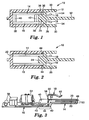
- Fig. 1 shows a sectional view of the novel plug 10 including a housing 12, which has, in the embodiment shown, a first housing part 26 and a second housing part 28.
- the first housing part 26 is adapted to face a telecommunications module (not shown), to which the plug 10 is fittable.
- the first housing part 26 includes two lateral protrusions 30 and one central protrusion 32, which is, in the embodiment shown, longer than the lateral protrusions 30.
- the protrusions are substantially parallel to each other.
- the protrusions 30, 32 can, for example, serve to position the plug relative to the telecommunications module.
- the central protrusion 32 can be insertable into a cavity formed in the telecommunications module, one result of which can be the proper positioning of the plug relative to the module.
- the central protrusion 32 can also serve to disconnect from each other the contacts of the telecommunications module that otherwise are in contact with each other at a disconnection point.
- plug contacts 18, which are exposed can establish electrical contact with the contacts of the telecommunications module.
- these contacts of the telecommunications module can, by the plug contacts 18, be connected with any functional components on printed circuit boards 14, 16 of the plug 10.
- plug contacts 18 are accommodated in recesses 34, which are formed between the central protrusion 32 and each of the lateral protrusions 30.
- the plug contacts 18 are, in the embodiment shown, shorter than the lateral protrusions 30, so that they are, particularly when the plug 10 is being handled before it is fitted to a telecommunications module or when it has been removed there from, protected against damage.
- the first housing part 26 is, in the embodiment shown, formed as a base and the second housing part 28 is formed as a type of cap so as to define an interior 36 of the housing 12.
- the first housing part 26 includes a spacer 24, which faces the interior 36.
- the spacer 24 is essentially formed as a comparably wide protrusion with steps 38 being defined on the sides thereof. These steps 38 are used to arrange the printed circuit boards 14, 16 and, particularly, space them from each other.
- that side of each printed circuit board 14, 16, which faces the other printed circuit board 16, 14 can be used for arranging functional components thereon.
- a spacer can be provided on one or both housing parts 26, 28. Such an embodiment is described below with reference to Fig. 2 .
- one or both housing parts 26, 28 can have suitable structures, such as one or more grooves, which are adapted to position a printed circuit board. Also in this way, two or more printed circuit boards can be kept in a fixed relationship to each other and be spaced from each other.
- a suitable structure such as a groove or a slot can be provided in one of the housing parts, for example, the second housing part 28, particularly at a location remote from the plug contacts 18.
- the plug contacts 18 can be fixed on the printed circuit board and the position of the plug contact 18 can be defined by the first and/or second housing part.
- the printed circuit board is in a defined position also on the side of the plug contacts 18.
- the printed circuit boards 14,16 are additionally electrically and mechanically connected with each other. This is, in the embodiment shown, achieved by two pins 40, 42. In the case shown, a first pin 42 is arranged relatively close to the spacer 24. The second pin 40 is arranged at a location remote from the spacer 24. This positioning enhances the mechanical stability of the arrangement. One or both pins 40, 42 can additionally be used to establish an electrical connection between the printed circuit boards 14, 16. As can also be seen in Fig. 1 , the printed circuit boards 14, 16 are arranged substantially parallel to each other.
- both printed circuit boards 14, 16 are arranged relatively close to the walls of the second housing part 28 so that, in the embodiment shown, the available space is efficiently used, for example, by arranging functional components on the printed circuit boards in the space that is present between them.
- Fig. 2 shows an embodiment similar to that of Fig. 1 .
- the main difference, compared with the embodiment of Fig. 1 is the arrangement of the printed circuit boards 14, 16.
- the printed circuit boards 14, 16 are mechanically attached to the spacer 24 provided on the first housing part 26 by fastening pins 44.
- the printed circuit boards 14, 16 entirely overlap each other.
- the printed circuit board are substantially the same size and overlie each other.
- One of the printed circuit board 14, 16 could be used to provide the functional components and circuits that are necessary to provide one or more splitter circuits.
- the other printed circuit board 16, 14 can be used to provide the components required for overvoltage and/or overcurrent protection.
- An optional opening, that can provide test access, is indicated at 22.
- Fig. 3 shows the printed circuit boards, functional components and contacts of a third embodiment of the novel plug.
- This embodiment differs from the above-described embodiments, firstly with regard to the arrangement of the printed circuit boards.
- the printed circuit boards 14, 16 are again arranged substantially parallel to each other. However, they only overlap in a small overlapping area 46 and are mechanically and/or electrically connected with each other by, in the embodiment shown, four pins 40.
- the first printed circuit board 14 itself has plug contacts formed thereon by providing contact sections 20 on the printed circuit board. These contact sections 20 are adapted to establish electrical connection with the contacts of a telecommunications module (not shown).
- a telecommunications module not shown.
- the printed circuit board 14 comprises a slit 48 so that two legs 50 are defined between the slit and each of the side edges of the approximately rectangular printed circuit board 14.
- at least two separate contact sections 20 can be provided. It can also be mentioned that further separate contact sections can be provided at the upper and lower side of each leg 50. Thus, for the embodiment shown, a total of four separate contact sections 20 can be defined.
- This opening 50 allows a plug contact 18 to pass through the first printed circuit board 14, so that it can be connected with the second printed circuit board 16.
- the plug contact 18 can, for example, be a grounding contact. Such a grounding contact can be provided for conducting overcurrent and/or overvoltage to ground.
- an overvoltage protector 54 with which the plug of Fig. 3 is equipped.
- Further functional components can be seen at 56.
- the functional components 54, 56 are, in the case shown, arranged on that side relative to printed circuit board 16, where also printed circuit board 14 is located.
- circuits (not visible in the drawing of Fig. 3 ) are provided on one or both printed circuit boards 14, 16, in order to allow the desired functions, such as protection, splitting, testing, coding etc., to be performed.
- the plug contact 18 has a first portion 58, which is substantially perpendicular to the second printed circuit board 16 and extends through the opening 52.
- a second portion 60 is bent approximately 90° with regard to the first portion 58 and comprises a flat V-shaped end 62. With this shape, reliable insertion and the establishment of electrical connection with a grounding element at the telecommunications module (not shown) can be achieved.
- resiliency of the plug contact 18 in the vertical direction of Fig. 3 can be used to provide a reliable electrical contact.
Claims (15)
- Stecker (10), enthaltend ein Gehäuse (12) und mindestens eine Funktionskomponente (54, 56), der mit Kontakten eines Telekommunikationsmoduls verbindbar ist, dadurch gekennzeichnet, dass der Stecker (10) mindestens zwei Leiterplatten (14, 16) enthält und die Leiterplatten getrennt mit Kontakten verbunden sind, die dazu ausgelegt sind, mit Kontakten eines Telekommunikationsmoduls verbunden zu werden.
- Stecker nach Anspruch 1, wobei mindestens zwei Leiterplatten (14, 16) im Wesentlichen parallel zueinander angeordnet sind.
- Stecker nach Anspruch 1 oder 2, wobei sich mindestens zwei Leiterplatten (14, 16) zumindest teilweise überlappen.
- Stecker nach einem der vorhergehenden Ansprüche, wobei mindestens zwei Leiterplatten (14, 16) elektrisch miteinander verbunden sind.
- Stecker nach einem der vorhergehenden Ansprüche, wobei mindestens zwei Leiterplatten (14, 16) mechanisch direkt miteinander verbunden sind.
- Stecker nach einem der vorhergehenden Ansprüche, wobei der Stecker (10) mindestens einen Steckerkontakt (18) enthält, der frei liegt, damit eine Verbindung mit einem Kontakt des Telekommunikationsmoduls hergestellt wird, und der sich durch mindestens eine Leiterplatte (16) hindurch erstreckt.
- Stecker nach einem der vorhergehenden Ansprüche, wobei mindestens eine der Leiterplatten (16) mindestens einen Kontaktabschnitt (20) daran enthält, der frei liegt, damit eine Verbindung mit einem Kontakt des Telekommunikationsmoduls hergestellt wird.
- Stecker nach einem der vorhergehenden Ansprüche, wobei mindestens eine Leiterplatte (14) mindestens eine Funktionskomponente (54, 56) an beiden Seiten davon enthält.
- Stecker nach einem der vorhergehenden Ansprüche, enthaltend mindestens eine Teilerschaltung.
- Stecker nach einem der vorhergehenden Ansprüche, enthaltend mindestens eine Schutzkomponente (54).
- Stecker nach einem der vorhergehenden Ansprüche, wobei das Gehäuse (12) mindestens eine Öffnung (22) enthält, die Prüfungszugang bietet.
- Stecker nach Anspruch 11, wobei der Prüfungszugang zur Durchführung von elektrischen Prüfungen, wie Isolierprüfung, Durchführungswiderstandsprüfung oder Übertragungsleistungsprüfung, verwendet werden kann.
- Stecker nach einem der vorhergehenden Ansprüche, wobei das Gehäuse mindestens einen Abstandhalter (24) enthält, der zwischen zwei Leiterplatten (14, 16) angeordnet ist.
- Anordnung, wie ein Verteilungspunkt, insbesondere ein Hauptverteiler, enthaltend mindestens ein Telekommunikationsmodul und mindestens einen Stecker (10) gemäß einem der vorhergehenden Ansprüche.
- Verfahren zur Herstellung eines Steckers nach Anspruch 1, enthaltend ein Gehäuse und mindestens eine Funktionskomponente, der mit Kontakten eines Telekommunikationsmoduls verbindbar ist, enthaltend den Schritt des Anbringens von mindestens zwei Leiterplatten an den Stecker.
Priority Applications (12)
| Application Number | Priority Date | Filing Date | Title |
|---|---|---|---|
| PL05021514T PL1770832T3 (pl) | 2005-09-30 | 2005-09-30 | Wtyczka telekomunikacyjna, zespół zawierający moduł telekomunikacyjny i wtyczkę oraz sposób wytwarzania wtyczki |
| ES05021514T ES2337066T3 (es) | 2005-09-30 | 2005-09-30 | Enchufe para telecomunicaciones, un conjunto que incluye un modulo de telecomunicaciones y un enchufe y un metodo de fabricacion de un enchufe. |
| DE602005018062T DE602005018062D1 (de) | 2005-09-30 | 2005-09-30 | Stecker für Telekommunikation, Anordnung mit einem Telekommunikationsmodul und einem Stecker, und Herstellungsverfahren für einen Stecker |
| EP05021514A EP1770832B1 (de) | 2005-09-30 | 2005-09-30 | Stecker für Telekommunikation, Anordnung mit einem Telekommunikationsmodul und einem Stecker, und Herstellungsverfahren für einen Stecker |
| AT05021514T ATE450909T1 (de) | 2005-09-30 | 2005-09-30 | Stecker für telekommunikation, anordnung mit einem telekommunikationsmodul und einem stecker, und herstellungsverfahren für einen stecker |
| US12/066,947 US20080318479A1 (en) | 2005-09-30 | 2006-09-25 | Plug in the Field of Telecommunications, an Assembly Including a Telecommunications Module and a Plug, and a Method of Manufacturing a Plug |
| PCT/US2006/037039 WO2007041034A1 (en) | 2005-09-30 | 2006-09-25 | A plug in the field of telecommunications, an assembly including a telecommunications module and a plug, and a method of manufacturing a plug |
| RU2008110408/09A RU2008110408A (ru) | 2005-09-30 | 2006-09-25 | Телекоммуникационный разъем и телекоммуникационное распределительное устройство |
| CNA2006800362294A CN101278445A (zh) | 2005-09-30 | 2006-09-25 | 电信领域的插头、包括电信模块和插头的组件以及制造该插头的方法 |
| BRPI0616614-8A BRPI0616614A2 (pt) | 2005-09-30 | 2006-09-25 | tomada no campo das telecomunicações, montagem que inclui uma tomada e módulo de telecomunicações, além de método para fabricação de uma tomada |
| TW095135699A TW200742191A (en) | 2005-09-30 | 2006-09-27 | A plug in the field of telecommunications, an assembly including a telecommunications module and a plug, and a method of manufacturing a plug |
| ARP060104327A AR055672A1 (es) | 2005-09-30 | 2006-10-02 | Un enchufe en el campo de las telecomunicaciones un esamble incluyendo un modulo de telecomunicaciones y enchufe y un metodo para manufacturar un enchufe |
Applications Claiming Priority (1)
| Application Number | Priority Date | Filing Date | Title |
|---|---|---|---|
| EP05021514A EP1770832B1 (de) | 2005-09-30 | 2005-09-30 | Stecker für Telekommunikation, Anordnung mit einem Telekommunikationsmodul und einem Stecker, und Herstellungsverfahren für einen Stecker |
Publications (2)
| Publication Number | Publication Date |
|---|---|
| EP1770832A1 EP1770832A1 (de) | 2007-04-04 |
| EP1770832B1 true EP1770832B1 (de) | 2009-12-02 |
Family
ID=35901840
Family Applications (1)
| Application Number | Title | Priority Date | Filing Date |
|---|---|---|---|
| EP05021514A Not-in-force EP1770832B1 (de) | 2005-09-30 | 2005-09-30 | Stecker für Telekommunikation, Anordnung mit einem Telekommunikationsmodul und einem Stecker, und Herstellungsverfahren für einen Stecker |
Country Status (12)
| Country | Link |
|---|---|
| US (1) | US20080318479A1 (de) |
| EP (1) | EP1770832B1 (de) |
| CN (1) | CN101278445A (de) |
| AR (1) | AR055672A1 (de) |
| AT (1) | ATE450909T1 (de) |
| BR (1) | BRPI0616614A2 (de) |
| DE (1) | DE602005018062D1 (de) |
| ES (1) | ES2337066T3 (de) |
| PL (1) | PL1770832T3 (de) |
| RU (1) | RU2008110408A (de) |
| TW (1) | TW200742191A (de) |
| WO (1) | WO2007041034A1 (de) |
Families Citing this family (3)
| Publication number | Priority date | Publication date | Assignee | Title |
|---|---|---|---|---|
| US8926339B2 (en) * | 2011-07-15 | 2015-01-06 | Fci Americas Technology Llc | Electrical connector having positioning assembly |
| CN105834684A (zh) * | 2016-04-26 | 2016-08-10 | 苏州昭沃五金科技有限公司 | 一种具有开口插孔的连接头加工工艺 |
| DE102016116926A1 (de) * | 2016-09-09 | 2018-03-15 | Harting Electric Gmbh & Co. Kg | Überspannungsschutzmodul für einen modularen Steckverbinder |
Family Cites Families (26)
| Publication number | Priority date | Publication date | Assignee | Title |
|---|---|---|---|---|
| CH504748A (de) * | 1970-02-11 | 1971-03-15 | Contraves Ag | Bauteilpaket für elektrische Ziffernanzeige |
| US4454566A (en) * | 1981-11-27 | 1984-06-12 | Bell Telephone Laboratories, Incorporated | Heat removal from cabinets housing electronic equipment |
| US4477857A (en) * | 1982-12-27 | 1984-10-16 | Gte Network Systems Corporation | Printed circuit fuse |
| DE3437988C3 (de) * | 1984-10-17 | 1996-11-21 | Bosch Gmbh Robert | Elektrisches Schaltgerät |
| US4744006A (en) * | 1986-07-10 | 1988-05-10 | Duffield Robert H | Apparatus for expanding the input/output capabilities of a personal computer |
| US4922374A (en) * | 1989-02-10 | 1990-05-01 | Illinois Tool Works, Inc. | Lightning protector assembly |
| US5155649A (en) * | 1989-10-02 | 1992-10-13 | Northern Telecom Limited | Surge protector for telecommunications equipment |
| US5260994A (en) * | 1991-09-25 | 1993-11-09 | Reliance Comm/Tec Corporation | Maintenance termination unit module |
| US5341269A (en) * | 1992-07-31 | 1994-08-23 | Illinois Tool Works Inc. | Voltage protector and grounding bar arrangement for terminal block |
| FR2708821A1 (fr) * | 1993-07-30 | 1995-02-10 | Amp France | Boîte d'interface d'abonné. |
| US5546267A (en) * | 1994-12-08 | 1996-08-13 | Illinois Tool Works Inc. | Communication circuit protector |
| US5718593A (en) * | 1995-07-03 | 1998-02-17 | Lucent Technologies Inc. | Polarity-sensitive protector device |
| US5920459A (en) * | 1997-02-04 | 1999-07-06 | The Whitaker Corporation | Electrical connector housing for circuit board assembly |
| US6438226B1 (en) * | 1997-10-06 | 2002-08-20 | Ccs Holdings, Inc. | XDSL splitter assembly for main distribution frame |
| US5999419A (en) * | 1998-08-07 | 1999-12-07 | National Semiconductor Corporation | Non-isolated boost converter with current steering |
| US6166894A (en) * | 1999-03-15 | 2000-12-26 | Lucent Technologies Inc. | PCB based protector cartridge |
| US6323743B1 (en) * | 1999-08-24 | 2001-11-27 | Tresness Irrevocable Patent Trust | Electronic filter assembly |
| DE29920935U1 (de) * | 1999-11-29 | 2000-02-03 | Quante Ag | Überspannungsschutzmagazin |
| DE10029649C9 (de) * | 2000-06-15 | 2008-02-07 | Adc Gmbh | Verteileranschlußmodul für die Telekommunikations- und Datentechnik |
| DE20104605U1 (de) * | 2001-03-16 | 2001-05-31 | 3M Innovative Properties Co | Anschlussblock und Verteilereinrichtung |
| US7103150B2 (en) * | 2001-09-05 | 2006-09-05 | Adc Telecommunications, Inc. | Splitter card with integral test access |
| DE20203910U1 (de) * | 2002-03-11 | 2003-07-17 | 3M Innovative Properties Co | Anschlussmodul der Telekommunikationstechnik |
| US6848943B2 (en) * | 2002-04-16 | 2005-02-01 | Pulse Engineering, Inc. | Shielded connector assembly and method of manufacturing |
| US6752664B2 (en) * | 2002-10-24 | 2004-06-22 | Hon Hai Precision Ind. Co., Ltd. | Modular jack having magnetic module with support and alignment mechanism |
| ATE494737T1 (de) * | 2003-03-03 | 2011-01-15 | 3M Innovative Properties Co | Anordnung von telekommunikationsmodulen mit wenigstens einem schutzstecker |
| KR100526506B1 (ko) * | 2003-05-27 | 2005-11-08 | 삼성전자주식회사 | 공기압 포설을 위한 광섬유 케이블 |
-
2005
- 2005-09-30 DE DE602005018062T patent/DE602005018062D1/de active Active
- 2005-09-30 EP EP05021514A patent/EP1770832B1/de not_active Not-in-force
- 2005-09-30 AT AT05021514T patent/ATE450909T1/de not_active IP Right Cessation
- 2005-09-30 PL PL05021514T patent/PL1770832T3/pl unknown
- 2005-09-30 ES ES05021514T patent/ES2337066T3/es active Active
-
2006
- 2006-09-25 BR BRPI0616614-8A patent/BRPI0616614A2/pt not_active IP Right Cessation
- 2006-09-25 WO PCT/US2006/037039 patent/WO2007041034A1/en active Application Filing
- 2006-09-25 US US12/066,947 patent/US20080318479A1/en not_active Abandoned
- 2006-09-25 CN CNA2006800362294A patent/CN101278445A/zh active Pending
- 2006-09-25 RU RU2008110408/09A patent/RU2008110408A/ru not_active Application Discontinuation
- 2006-09-27 TW TW095135699A patent/TW200742191A/zh unknown
- 2006-10-02 AR ARP060104327A patent/AR055672A1/es unknown
Also Published As
| Publication number | Publication date |
|---|---|
| EP1770832A1 (de) | 2007-04-04 |
| BRPI0616614A2 (pt) | 2011-06-28 |
| WO2007041034A1 (en) | 2007-04-12 |
| US20080318479A1 (en) | 2008-12-25 |
| TW200742191A (en) | 2007-11-01 |
| AR055672A1 (es) | 2007-08-29 |
| PL1770832T3 (pl) | 2010-05-31 |
| RU2008110408A (ru) | 2009-11-10 |
| CN101278445A (zh) | 2008-10-01 |
| ATE450909T1 (de) | 2009-12-15 |
| DE602005018062D1 (de) | 2010-01-14 |
| ES2337066T3 (es) | 2010-04-20 |
Similar Documents
| Publication | Publication Date | Title |
|---|---|---|
| EP1750337B1 (de) | Überspannungsschutzmodul und Zusammenbau von mindestens einem Telekommunikationsmodul und mindestens einem Überspannungsschutzmodul | |
| US7207818B1 (en) | Telecommunications assembly including at least one telecommunications module | |
| EP1804523B1 (de) | Telekommunikationsmodul und Telekommunikationsanordnung mit mindestens einem Telekommunikationsmodul | |
| EP1770832B1 (de) | Stecker für Telekommunikation, Anordnung mit einem Telekommunikationsmodul und einem Stecker, und Herstellungsverfahren für einen Stecker | |
| US7892046B2 (en) | Telecommunications module, combination of a telecommunications module and at least one splitter circuit, and assembly of at least two telecommunications modules | |
| US20070223684A1 (en) | Modular Arrangement in the Field of Telecommunications | |
| EP1455543A1 (de) | Anordnung von Telekommunikationsmodulen mit wenigstens einem Schutzstecker | |
| US20080153357A1 (en) | Telecommunications Module, Assemblies Thereof and Methods of Making and Using Same | |
| EP2553939B1 (de) | Telekommunikationsmodul mit trennfunktion | |
| US20070275606A1 (en) | Telecommunications module and combination including at least one telecommunicatins module | |
| CN101133520A (zh) | 电信模块及其组件和使用该电信模块的方法 | |
| US20090253310A1 (en) | Telecommunications assembly including at least one telecommunications module, a test bus and a kit of parts |
Legal Events
| Date | Code | Title | Description |
|---|---|---|---|
| PUAI | Public reference made under article 153(3) epc to a published international application that has entered the european phase |
Free format text: ORIGINAL CODE: 0009012 |
|
| AK | Designated contracting states |
Kind code of ref document: A1 Designated state(s): AT BE BG CH CY CZ DE DK EE ES FI FR GB GR HU IE IS IT LI LT LU LV MC NL PL PT RO SE SI SK TR |
|
| AX | Request for extension of the european patent |
Extension state: AL BA HR MK YU |
|
| 17P | Request for examination filed |
Effective date: 20070824 |
|
| 17Q | First examination report despatched |
Effective date: 20071001 |
|
| AKX | Designation fees paid |
Designated state(s): AT BE BG CH CY CZ DE DK EE ES FI FR GB GR HU IE IS IT LI LT LU LV MC NL PL PT RO SE SI SK TR |
|
| GRAP | Despatch of communication of intention to grant a patent |
Free format text: ORIGINAL CODE: EPIDOSNIGR1 |
|
| GRAS | Grant fee paid |
Free format text: ORIGINAL CODE: EPIDOSNIGR3 |
|
| GRAA | (expected) grant |
Free format text: ORIGINAL CODE: 0009210 |
|
| AK | Designated contracting states |
Kind code of ref document: B1 Designated state(s): AT BE BG CH CY CZ DE DK EE ES FI FR GB GR HU IE IS IT LI LT LU LV MC NL PL PT RO SE SI SK TR |
|
| REG | Reference to a national code |
Ref country code: GB Ref legal event code: FG4D |
|
| REG | Reference to a national code |
Ref country code: CH Ref legal event code: EP |
|
| REG | Reference to a national code |
Ref country code: IE Ref legal event code: FG4D |
|
| REF | Corresponds to: |
Ref document number: 602005018062 Country of ref document: DE Date of ref document: 20100114 Kind code of ref document: P |
|
| REG | Reference to a national code |
Ref country code: NL Ref legal event code: VDEP Effective date: 20091202 |
|
| REG | Reference to a national code |
Ref country code: ES Ref legal event code: FG2A Ref document number: 2337066 Country of ref document: ES Kind code of ref document: T3 |
|
| PG25 | Lapsed in a contracting state [announced via postgrant information from national office to epo] |
Ref country code: FI Free format text: LAPSE BECAUSE OF FAILURE TO SUBMIT A TRANSLATION OF THE DESCRIPTION OR TO PAY THE FEE WITHIN THE PRESCRIBED TIME-LIMIT Effective date: 20091202 Ref country code: SE Free format text: LAPSE BECAUSE OF FAILURE TO SUBMIT A TRANSLATION OF THE DESCRIPTION OR TO PAY THE FEE WITHIN THE PRESCRIBED TIME-LIMIT Effective date: 20091202 Ref country code: LT Free format text: LAPSE BECAUSE OF FAILURE TO SUBMIT A TRANSLATION OF THE DESCRIPTION OR TO PAY THE FEE WITHIN THE PRESCRIBED TIME-LIMIT Effective date: 20091202 |
|
| LTIE | Lt: invalidation of european patent or patent extension |
Effective date: 20091202 |
|
| PG25 | Lapsed in a contracting state [announced via postgrant information from national office to epo] |
Ref country code: SI Free format text: LAPSE BECAUSE OF FAILURE TO SUBMIT A TRANSLATION OF THE DESCRIPTION OR TO PAY THE FEE WITHIN THE PRESCRIBED TIME-LIMIT Effective date: 20091202 Ref country code: CY Free format text: LAPSE BECAUSE OF FAILURE TO SUBMIT A TRANSLATION OF THE DESCRIPTION OR TO PAY THE FEE WITHIN THE PRESCRIBED TIME-LIMIT Effective date: 20091202 Ref country code: LV Free format text: LAPSE BECAUSE OF FAILURE TO SUBMIT A TRANSLATION OF THE DESCRIPTION OR TO PAY THE FEE WITHIN THE PRESCRIBED TIME-LIMIT Effective date: 20091202 |
|
| REG | Reference to a national code |
Ref country code: PL Ref legal event code: T3 |
|
| PG25 | Lapsed in a contracting state [announced via postgrant information from national office to epo] |
Ref country code: AT Free format text: LAPSE BECAUSE OF FAILURE TO SUBMIT A TRANSLATION OF THE DESCRIPTION OR TO PAY THE FEE WITHIN THE PRESCRIBED TIME-LIMIT Effective date: 20091202 |
|
| PG25 | Lapsed in a contracting state [announced via postgrant information from national office to epo] |
Ref country code: IS Free format text: LAPSE BECAUSE OF FAILURE TO SUBMIT A TRANSLATION OF THE DESCRIPTION OR TO PAY THE FEE WITHIN THE PRESCRIBED TIME-LIMIT Effective date: 20100402 Ref country code: RO Free format text: LAPSE BECAUSE OF FAILURE TO SUBMIT A TRANSLATION OF THE DESCRIPTION OR TO PAY THE FEE WITHIN THE PRESCRIBED TIME-LIMIT Effective date: 20091202 Ref country code: EE Free format text: LAPSE BECAUSE OF FAILURE TO SUBMIT A TRANSLATION OF THE DESCRIPTION OR TO PAY THE FEE WITHIN THE PRESCRIBED TIME-LIMIT Effective date: 20091202 Ref country code: PT Free format text: LAPSE BECAUSE OF FAILURE TO SUBMIT A TRANSLATION OF THE DESCRIPTION OR TO PAY THE FEE WITHIN THE PRESCRIBED TIME-LIMIT Effective date: 20100402 Ref country code: NL Free format text: LAPSE BECAUSE OF FAILURE TO SUBMIT A TRANSLATION OF THE DESCRIPTION OR TO PAY THE FEE WITHIN THE PRESCRIBED TIME-LIMIT Effective date: 20091202 Ref country code: BG Free format text: LAPSE BECAUSE OF FAILURE TO SUBMIT A TRANSLATION OF THE DESCRIPTION OR TO PAY THE FEE WITHIN THE PRESCRIBED TIME-LIMIT Effective date: 20100302 |
|
| PG25 | Lapsed in a contracting state [announced via postgrant information from national office to epo] |
Ref country code: CZ Free format text: LAPSE BECAUSE OF FAILURE TO SUBMIT A TRANSLATION OF THE DESCRIPTION OR TO PAY THE FEE WITHIN THE PRESCRIBED TIME-LIMIT Effective date: 20091202 Ref country code: SK Free format text: LAPSE BECAUSE OF FAILURE TO SUBMIT A TRANSLATION OF THE DESCRIPTION OR TO PAY THE FEE WITHIN THE PRESCRIBED TIME-LIMIT Effective date: 20091202 Ref country code: BE Free format text: LAPSE BECAUSE OF FAILURE TO SUBMIT A TRANSLATION OF THE DESCRIPTION OR TO PAY THE FEE WITHIN THE PRESCRIBED TIME-LIMIT Effective date: 20091202 |
|
| PLBE | No opposition filed within time limit |
Free format text: ORIGINAL CODE: 0009261 |
|
| STAA | Information on the status of an ep patent application or granted ep patent |
Free format text: STATUS: NO OPPOSITION FILED WITHIN TIME LIMIT |
|
| PG25 | Lapsed in a contracting state [announced via postgrant information from national office to epo] |
Ref country code: GR Free format text: LAPSE BECAUSE OF FAILURE TO SUBMIT A TRANSLATION OF THE DESCRIPTION OR TO PAY THE FEE WITHIN THE PRESCRIBED TIME-LIMIT Effective date: 20100303 |
|
| 26N | No opposition filed |
Effective date: 20100903 |
|
| PG25 | Lapsed in a contracting state [announced via postgrant information from national office to epo] |
Ref country code: DK Free format text: LAPSE BECAUSE OF FAILURE TO SUBMIT A TRANSLATION OF THE DESCRIPTION OR TO PAY THE FEE WITHIN THE PRESCRIBED TIME-LIMIT Effective date: 20091202 |
|
| PG25 | Lapsed in a contracting state [announced via postgrant information from national office to epo] |
Ref country code: IT Free format text: LAPSE BECAUSE OF FAILURE TO SUBMIT A TRANSLATION OF THE DESCRIPTION OR TO PAY THE FEE WITHIN THE PRESCRIBED TIME-LIMIT Effective date: 20091202 |
|
| PG25 | Lapsed in a contracting state [announced via postgrant information from national office to epo] |
Ref country code: MC Free format text: LAPSE BECAUSE OF NON-PAYMENT OF DUE FEES Effective date: 20100930 |
|
| REG | Reference to a national code |
Ref country code: CH Ref legal event code: PL |
|
| GBPC | Gb: european patent ceased through non-payment of renewal fee |
Effective date: 20100930 |
|
| REG | Reference to a national code |
Ref country code: FR Ref legal event code: ST Effective date: 20110531 |
|
| REG | Reference to a national code |
Ref country code: DE Ref legal event code: R119 Ref document number: 602005018062 Country of ref document: DE Effective date: 20110401 |
|
| PG25 | Lapsed in a contracting state [announced via postgrant information from national office to epo] |
Ref country code: FR Free format text: LAPSE BECAUSE OF NON-PAYMENT OF DUE FEES Effective date: 20100930 Ref country code: LI Free format text: LAPSE BECAUSE OF NON-PAYMENT OF DUE FEES Effective date: 20100930 Ref country code: CH Free format text: LAPSE BECAUSE OF NON-PAYMENT OF DUE FEES Effective date: 20100930 Ref country code: DE Free format text: LAPSE BECAUSE OF NON-PAYMENT OF DUE FEES Effective date: 20110401 Ref country code: IE Free format text: LAPSE BECAUSE OF NON-PAYMENT OF DUE FEES Effective date: 20100930 |
|
| PG25 | Lapsed in a contracting state [announced via postgrant information from national office to epo] |
Ref country code: GB Free format text: LAPSE BECAUSE OF NON-PAYMENT OF DUE FEES Effective date: 20100930 |
|
| REG | Reference to a national code |
Ref country code: ES Ref legal event code: FD2A Effective date: 20111019 |
|
| PG25 | Lapsed in a contracting state [announced via postgrant information from national office to epo] |
Ref country code: ES Free format text: LAPSE BECAUSE OF NON-PAYMENT OF DUE FEES Effective date: 20101001 |
|
| PG25 | Lapsed in a contracting state [announced via postgrant information from national office to epo] |
Ref country code: PL Free format text: LAPSE BECAUSE OF NON-PAYMENT OF DUE FEES Effective date: 20100930 |
|
| REG | Reference to a national code |
Ref country code: PL Ref legal event code: LAPE |
|
| PG25 | Lapsed in a contracting state [announced via postgrant information from national office to epo] |
Ref country code: HU Free format text: LAPSE BECAUSE OF FAILURE TO SUBMIT A TRANSLATION OF THE DESCRIPTION OR TO PAY THE FEE WITHIN THE PRESCRIBED TIME-LIMIT Effective date: 20100603 Ref country code: LU Free format text: LAPSE BECAUSE OF NON-PAYMENT OF DUE FEES Effective date: 20100930 |
|
| PG25 | Lapsed in a contracting state [announced via postgrant information from national office to epo] |
Ref country code: TR Free format text: LAPSE BECAUSE OF FAILURE TO SUBMIT A TRANSLATION OF THE DESCRIPTION OR TO PAY THE FEE WITHIN THE PRESCRIBED TIME-LIMIT Effective date: 20091202 |