EP1765175B1 - Ultrasonic probe and method for the fabrication thereof - Google Patents
Ultrasonic probe and method for the fabrication thereof Download PDFInfo
- Publication number
- EP1765175B1 EP1765175B1 EP04733484.2A EP04733484A EP1765175B1 EP 1765175 B1 EP1765175 B1 EP 1765175B1 EP 04733484 A EP04733484 A EP 04733484A EP 1765175 B1 EP1765175 B1 EP 1765175B1
- Authority
- EP
- European Patent Office
- Prior art keywords
- piezoelectric element
- electrode
- face
- grooves
- circuit board
- Prior art date
- Legal status (The legal status is an assumption and is not a legal conclusion. Google has not performed a legal analysis and makes no representation as to the accuracy of the status listed.)
- Expired - Lifetime
Links
- 239000000523 sample Substances 0.000 title claims description 37
- 238000000034 method Methods 0.000 title claims description 18
- 238000004519 manufacturing process Methods 0.000 title claims description 6
- 239000004593 Epoxy Substances 0.000 claims description 14
- 239000013078 crystal Substances 0.000 claims description 10
- 229910052709 silver Inorganic materials 0.000 claims description 5
- BQCADISMDOOEFD-UHFFFAOYSA-N Silver Chemical compound [Ag] BQCADISMDOOEFD-UHFFFAOYSA-N 0.000 claims description 4
- 238000005452 bending Methods 0.000 claims description 4
- 239000004332 silver Substances 0.000 claims description 4
- 238000000151 deposition Methods 0.000 claims description 2
- 239000000758 substrate Substances 0.000 description 8
- 230000000052 comparative effect Effects 0.000 description 7
- 229910052751 metal Inorganic materials 0.000 description 6
- 239000002184 metal Substances 0.000 description 6
- 239000012071 phase Substances 0.000 description 4
- 230000035945 sensitivity Effects 0.000 description 4
- 230000007704 transition Effects 0.000 description 4
- 229910003781 PbTiO3 Inorganic materials 0.000 description 3
- 238000002955 isolation Methods 0.000 description 3
- 229910052451 lead zirconate titanate Inorganic materials 0.000 description 3
- 229910019653 Mg1/3Nb2/3 Inorganic materials 0.000 description 2
- MCMNRKCIXSYSNV-UHFFFAOYSA-N Zirconium dioxide Chemical compound O=[Zr]=O MCMNRKCIXSYSNV-UHFFFAOYSA-N 0.000 description 2
- 239000011248 coating agent Substances 0.000 description 2
- 238000000576 coating method Methods 0.000 description 2
- 229910052802 copper Inorganic materials 0.000 description 2
- 229910052737 gold Inorganic materials 0.000 description 2
- 230000000873 masking effect Effects 0.000 description 2
- 229910052759 nickel Inorganic materials 0.000 description 2
- 238000012545 processing Methods 0.000 description 2
- 238000004544 sputter deposition Methods 0.000 description 2
- 229910012463 LiTaO3 Inorganic materials 0.000 description 1
- FYYHWMGAXLPEAU-UHFFFAOYSA-N Magnesium Chemical compound [Mg] FYYHWMGAXLPEAU-UHFFFAOYSA-N 0.000 description 1
- 229910052793 cadmium Inorganic materials 0.000 description 1
- 239000000919 ceramic Substances 0.000 description 1
- 229910052804 chromium Inorganic materials 0.000 description 1
- 230000008878 coupling Effects 0.000 description 1
- 238000010168 coupling process Methods 0.000 description 1
- 238000005859 coupling reaction Methods 0.000 description 1
- 238000002425 crystallisation Methods 0.000 description 1
- 230000001419 dependent effect Effects 0.000 description 1
- 230000008021 deposition Effects 0.000 description 1
- 238000003745 diagnosis Methods 0.000 description 1
- 239000007772 electrode material Substances 0.000 description 1
- 238000009713 electroplating Methods 0.000 description 1
- 238000003384 imaging method Methods 0.000 description 1
- 238000003780 insertion Methods 0.000 description 1
- 230000037431 insertion Effects 0.000 description 1
- HFGPZNIAWCZYJU-UHFFFAOYSA-N lead zirconate titanate Chemical compound [O-2].[O-2].[O-2].[O-2].[O-2].[Ti+4].[Zr+4].[Pb+2] HFGPZNIAWCZYJU-UHFFFAOYSA-N 0.000 description 1
- 229910052749 magnesium Inorganic materials 0.000 description 1
- 239000011777 magnesium Substances 0.000 description 1
- 238000012986 modification Methods 0.000 description 1
- 230000004048 modification Effects 0.000 description 1
- 229910052763 palladium Inorganic materials 0.000 description 1
- 229910052697 platinum Inorganic materials 0.000 description 1
- 230000008569 process Effects 0.000 description 1
- 230000004044 response Effects 0.000 description 1
- 229910052703 rhodium Inorganic materials 0.000 description 1
- 238000005476 soldering Methods 0.000 description 1
- 238000003746 solid phase reaction Methods 0.000 description 1
- 238000012360 testing method Methods 0.000 description 1
- 238000002207 thermal evaporation Methods 0.000 description 1
- 230000002463 transducing effect Effects 0.000 description 1
Images





Classifications
-
- B—PERFORMING OPERATIONS; TRANSPORTING
- B06—GENERATING OR TRANSMITTING MECHANICAL VIBRATIONS IN GENERAL
- B06B—METHODS OR APPARATUS FOR GENERATING OR TRANSMITTING MECHANICAL VIBRATIONS OF INFRASONIC, SONIC, OR ULTRASONIC FREQUENCY, e.g. FOR PERFORMING MECHANICAL WORK IN GENERAL
- B06B1/00—Methods or apparatus for generating mechanical vibrations of infrasonic, sonic, or ultrasonic frequency
- B06B1/02—Methods or apparatus for generating mechanical vibrations of infrasonic, sonic, or ultrasonic frequency making use of electrical energy
- B06B1/06—Methods or apparatus for generating mechanical vibrations of infrasonic, sonic, or ultrasonic frequency making use of electrical energy operating with piezoelectric effect or with electrostriction
- B06B1/0644—Methods or apparatus for generating mechanical vibrations of infrasonic, sonic, or ultrasonic frequency making use of electrical energy operating with piezoelectric effect or with electrostriction using a single piezoelectric element
- B06B1/0662—Methods or apparatus for generating mechanical vibrations of infrasonic, sonic, or ultrasonic frequency making use of electrical energy operating with piezoelectric effect or with electrostriction using a single piezoelectric element with an electrode on the sensitive surface
- B06B1/0677—Methods or apparatus for generating mechanical vibrations of infrasonic, sonic, or ultrasonic frequency making use of electrical energy operating with piezoelectric effect or with electrostriction using a single piezoelectric element with an electrode on the sensitive surface and a high impedance backing
-
- B—PERFORMING OPERATIONS; TRANSPORTING
- B06—GENERATING OR TRANSMITTING MECHANICAL VIBRATIONS IN GENERAL
- B06B—METHODS OR APPARATUS FOR GENERATING OR TRANSMITTING MECHANICAL VIBRATIONS OF INFRASONIC, SONIC, OR ULTRASONIC FREQUENCY, e.g. FOR PERFORMING MECHANICAL WORK IN GENERAL
- B06B1/00—Methods or apparatus for generating mechanical vibrations of infrasonic, sonic, or ultrasonic frequency
- B06B1/02—Methods or apparatus for generating mechanical vibrations of infrasonic, sonic, or ultrasonic frequency making use of electrical energy
- B06B1/06—Methods or apparatus for generating mechanical vibrations of infrasonic, sonic, or ultrasonic frequency making use of electrical energy operating with piezoelectric effect or with electrostriction
- B06B1/0644—Methods or apparatus for generating mechanical vibrations of infrasonic, sonic, or ultrasonic frequency making use of electrical energy operating with piezoelectric effect or with electrostriction using a single piezoelectric element
- B06B1/0662—Methods or apparatus for generating mechanical vibrations of infrasonic, sonic, or ultrasonic frequency making use of electrical energy operating with piezoelectric effect or with electrostriction using a single piezoelectric element with an electrode on the sensitive surface
- B06B1/0681—Methods or apparatus for generating mechanical vibrations of infrasonic, sonic, or ultrasonic frequency making use of electrical energy operating with piezoelectric effect or with electrostriction using a single piezoelectric element with an electrode on the sensitive surface and a damping structure
- B06B1/0685—Methods or apparatus for generating mechanical vibrations of infrasonic, sonic, or ultrasonic frequency making use of electrical energy operating with piezoelectric effect or with electrostriction using a single piezoelectric element with an electrode on the sensitive surface and a damping structure on the back only of piezoelectric elements
Definitions
- the present invention relates to an ultrasonic probe having uniquely designed electrodes, and a method for the fabrication thereof.
- US 5,810,009 A relates to an ultrasonic probe and a method of manufacturing said probe.
- Ultrasonic imaging equipments have been widely used, and they conventionally comprise an ultrasonic probe for transducing an ultrasonic wave to an electric signal, a processing unit for processing the electric signal to an image and a display unit for displaying the image.
- the ultrasonic probe plays an important role in obtaining high-resolution image, and it is required to have a high electromechanical coupling coefficient, as well as good ultrasonic wave pulse and focusing characteristics of ultrasonic beam.
- An ultrasonic probe typically comprises an ultrasonic transmitting/receiving element consisting essentially of a piezoelectric element having a pair of electrodes, and as the piezoelectric element, lead zirconate titanate-based ceramics (PZT) was previously employed, but recently, a lead zirconia niobate-lead titanate(Pb(Zn 1/3 Nb 2/3 )0 3 -PbTiO 3 ; "PZN-PT”)- or lead magnesium niobate-lead titanate (Pb(Mg 1/3 Nb 2/3 )0 3 -PbTi0 3 ; "PMN-PT”) based piezoelectric single crystals have become favored because of their better properties.
- PZT lead zirconate titanate-based ceramics
- PZN-PT and PMN-PT have the disadvantage of poor thermal stability due to a low phase transition temperature.
- PZT has a phase transition temperature range of about 200 to 385 °C
- 0.67PMN-0.33PT exhibits the phase transition phenomena at about 150 °C. If a piezoelectric element is subjected to a temperature higher than the phase transition temperature, it will become depolarized, and thus, the preparing process of an ultrasonic probe using such piezoelectric elements should not involve a high-temperature step.
- the electrical connection in an ultrasonic probe has been often achieved by using an epoxy paste which does not require a high temperature, rather than by soldering.
- an epoxy paste layer tends to degrade the performance of the ultrasonic probe, and the connection of a flexible printed circuit board (FPCB) thereto requires an elaborate fabrication procedure.
- FPCB flexible printed circuit board
- a primary object of the invention to provide a novel ultrasonic probe comprising a piezoelectric element having uniquely designed electrodes and FPCB attached thereto in a way which is not influenced by the paste used for the attachment.
- an ultrasonic probe as defined in claim 1.
- the inventive ultrasonic probe is characterized by comprising uniquely designed electrodes and FPCB attached thereto in a form not influenced by the paste used for the attachment.
- An ultrasonic probe conventionally contains a piezoelectric device (an ultrasonic transmitting/receiving element) comprising a piezoelectric element consisting essentially of a piezoelectric single crystal; a first and second electrodes formed on an ultrasonic wave transmitting/receiving face and the face opposite to the transmitting/receiving face of the piezoelectric element, respectively; acoustic matching layers formed on the first electrode; an acoustic lens formed to cover the entire surface of the acoustic matching layer; a ground electrode connected to the first electrode; and a flexible printed circuit board for signal, connected to the second electrode.
- a piezoelectric device an ultrasonic transmitting/receiving element
- a piezoelectric element consisting essentially of a piezoelectric single crystal
- first and second electrodes formed on an ultrasonic wave transmitting/receiving face and the face opposite to the transmitting/receiving face of the piezoelectric element, respectively
- the inventive ultrasonic probe is characterized in that the first electrode is formed on a substantial portion of a first main face, a first side face and a part of a second main face of the piezoelectric element, and the second electrode is formed on a substantial portion of a second main face, a second side face and a part of a first main face of the piezoelectric element, and that the two electrodes are isolated from each other by two grooves formed on the first and second main faces of the piezoelectric element, in a manner parallel to the side edges of the piezoelectric element, respectively, at positions separated from the second and first side edges by a given distance, respectively.
- the inventive ultrasonic probe may be fabricated as shown in Figs. 2 and 3 .
- electrode layer 20" is deposited on the first and second main faces 10a, 10b and the first and second side faces 10c, 10d of single crystal piezoelectric element or wafer 10 (see Fig. 2a ), to obtain a coated wafer (see Fig. 2b ).
- the piezoelectric element may have a thickness of 20 to 500,000 ⁇ m, preferably 50 to 400 ⁇ m, in the direction of vibration.
- the electrode layer may be made of a conductive metal such as Cr, Cu, Ni, Au, etc., and a combination thereof.
- the deposition of the electrode layer may be conducted using a sputtering, electronic-beam, thermal-evaporation or electroplating method, and the thickness of the deposited electrode may range from 100 to 10,000 ⁇ .
- first electrode 20 formed mainly on first main face 10a and first side face 10c (an ultrasonic wave transmitting/receiving face)
- second electrode 20' formed mainly on second main face 10b and second side face 10d (the face opposite to the transmitting/receiving face), as shown in Fig. 2c .
- the grooves 30, 30' may each be formed at a position separated from the side edge of the piezoelectric element by a given distance, for example a distance to make room for applying an epoxy paste to attach the electrode to a flexible printed circuit board or a ground electrode in a later step, using a dicing saw.
- the grooves may be formed at the position of 1 to 1.5 mm inwardly from each side edge, and according to the invention, to a depth corresponding to 70 to 80% of the wafer thickness, in order to inhibit the generation of undesirable vibration.
- the resulting assembly 100 is then used to fabricate the inventive ultrasonic probe, as shown in Figs. 3a to 3d .
- Fig. 3a shows the step of attaching backing layer 40 to the electrode layer deposited on second main face 10b of the piezoelectric element, using an epoxy paste in a conventional manner
- Fig. 3b shows the step of attaching ground electrode plate 50 and flexible printed circuit board 60 for signal.
- ground electrode plate 50 is attached to first electrode 20 at first side face 10c of piezoelectric element 10
- flexible printed circuit board 60 is attached to second electrode 20' in the front portion of the groove 30 positioned on first main face 10a of the piezoelectric element, extending from second side face 10d of the piezoelectric element, and bending at the end part at a right angle.
- the attachment of the ground electrode plate and the flexible printed circuit board to the first and second electrodes, respectively, may be conventionally carried out using conductive epoxy paste 70, preferably a conductive silver epoxy paste, as shown in Fig. 3c , and the use of such bended end part make the bonding of the electrode with the flexible printed circuit board strong.
- At least one acoustic matching layer 80 may be formed on the electrode layer deposited on the first main face of the piezoelectric element, as in Fig. 3d , and thereon an acoustic lens may be covered.
- the ultrasonic probe fabricated by the inventive method can have excellent vibration characteristics, a wide frequency band, and a high sensitivity.
- the piezoelectric single crystal used in the ultrasonic probe may be any strongly ferroelectric, homogeneous single crystal, preferably PMN-PT, of which an example may have the composition of formula (I): x(A)y(B)z(C)-p(P)n(N) (I) wherein,
- the single crystal of formula (I) may be prepared by way of conducting a solid phase reaction followed by melting-crystallization, by a method described in Korean Patent No. 392754 .
- the piezoelectric single crystal of formula (I) has a high dielectric constant of about 5,500 or higher, a piezoelectric constant of about 1,500 pC/N or higher at an ambient temperature, and a low temperature coefficient in a broad temperature range of 20 to 90°C.
- the inventive ultrasonic probe has a relative dielectric constant ranging from about 1,000 to 10,000, the velocity of a sound wave generated on the (001) face ranging from 1,200 to 4,000 m/s (frequency constant: 1,400 to 2,000 Hz.m), and a high electromechanical coefficient (k 33 ') ranging from 80 to 95%. Accordingly, the inventive ultrasonic probe can be beneficially used for an ultrasonic diagnosis in medical, military, and industrial fields.
- An ultrasonic probe as shown in Fig. 1 was fabricated by a method comprising the procedures as shown in Figs. 2 and 3 .
- Piezoelectric single crystal substrate 10 having a (001) face (surface 10a) and a size of 20-25mm x 15-20mm x 0.4-0.5mm was prepared, and metal layer (Cr/Cu/Au) 20" was deposited using a DC sputtering method on surfaces10a, 10b, 10c and 10d of the substrate (but not on surfaces 10e and 10f) at an ambient temperature under a pressure of 1.2 x 10 -7 mmHg ( Figs. 2a and 2b ).
- grooves 30 and 30' were formed on surfaces 10a and 10 b of the metal deposited piezoelectric single crystal substrate, respectively, to separate metal layer 20" into two electrodes 20 and 20' by using a dicing saw: Groove 30 was formed on electrode layer 20" deposited on surface 10a in a manner parallel to the edge formed with surface 10d at a distance of 1-1.5 mm from said edge, while groove 30' was formed on electrode layer 20" deposited on surface 10b at a distance of 1-1.5 mm from the side edge with surface 10c of the substrate ( Fig. 2c ). Each of two grooves 30, 30' had a depth of 0.25-0.35 mm.
- Backing layer 40 was laminated on the electrode layer deposited on surface 10b of piezoelectric substrate 10 using an epoxy paste ( Fig. 3a ), and ground electrode plate 50 was attached to electrode 20 at first side face 10c of piezoelectric substrate 10 while flexible printed circuit board 60 was attached to electrode 20' at a part of the front of groove 30, beyond second side face 10d, of piezoelectric substrate 10, by bending at a right angle ( Fig. 3b ). Thereafter, two acoustic matching layers 80 were laminated on the electrode layer deposited on surface 10a of piezoelectric substrate 10, and thereon an acoustic lens was covered to fabricate the inventive ultrasonic probe, as shown in Fig. 1 .
- Example 2 The procedures of Example were repeated except that the two electrodes 20, 20' were formed by coating an electrode material after a masking tape was covered on the isolation portions 30, 30' and then removing the masking tape after coating, to fabricate an ultrasonic probe.
- Fig. 4b it can be seen that the piezoelectric element according to Comparative Example generates an undesirable vibration as shown in a dot-line box.
- Fig. 4a shows that such undesirable vibration did not appear in the piezoelectric element according to the present invention.
- the inventive probe comprising electrodes isolated by grooves having a given depth gives improved vibration performance.
- the probing characteristics (the relative sensitivity and the band-width) of the ultrasonic probes fabricated in Example and Comparative Example were measured with a pulse-echo response test, and the results are shown in Table 1.
- Table 1 shows that the inventive probe having electrode isolation grooves is better in terms of sensitivity and band-width than the probe of Comparative Example having a simple isolation portion.
Landscapes
- Engineering & Computer Science (AREA)
- Mechanical Engineering (AREA)
- Ultra Sonic Daignosis Equipment (AREA)
- Transducers For Ultrasonic Waves (AREA)
- Investigating Or Analyzing Materials By The Use Of Ultrasonic Waves (AREA)
Description
- The present invention relates to an ultrasonic probe having uniquely designed electrodes, and a method for the fabrication thereof.
-
US 5,810,009 A relates to an ultrasonic probe and a method of manufacturing said probe. Ultrasonic imaging equipments have been widely used, and they conventionally comprise an ultrasonic probe for transducing an ultrasonic wave to an electric signal, a processing unit for processing the electric signal to an image and a display unit for displaying the image. The ultrasonic probe plays an important role in obtaining high-resolution image, and it is required to have a high electromechanical coupling coefficient, as well as good ultrasonic wave pulse and focusing characteristics of ultrasonic beam. - An ultrasonic probe typically comprises an ultrasonic transmitting/receiving element consisting essentially of a piezoelectric element having a pair of electrodes, and as the piezoelectric element, lead zirconate titanate-based ceramics (PZT) was previously employed, but recently, a lead zirconia niobate-lead titanate(Pb(Zn1/3Nb2/3)03-PbTiO3; "PZN-PT")- or lead magnesium niobate-lead titanate (Pb(Mg1/3Nb2/3)03-PbTi03; "PMN-PT") based piezoelectric single crystals have become favored because of their better properties. However, PZN-PT and PMN-PT have the disadvantage of poor thermal stability due to a low phase transition temperature. For example, while PZT has a phase transition temperature range of about 200 to 385 °C, 0.67PMN-0.33PT exhibits the phase transition phenomena at about 150 °C. If a piezoelectric element is subjected to a temperature higher than the phase transition temperature, it will become depolarized, and thus, the preparing process of an ultrasonic probe using such piezoelectric elements should not involve a high-temperature step.
- Accordingly, the electrical connection in an ultrasonic probe has been often achieved by using an epoxy paste which does not require a high temperature, rather than by soldering. However, the insertion of an epoxy paste layer tends to degrade the performance of the ultrasonic probe, and the connection of a flexible printed circuit board (FPCB) thereto requires an elaborate fabrication procedure. Although a silver epoxy paste having a better conductivity than a non-silver epoxy paste has been used in an attempt to reduce the thickness of the epoxy paste layer, the above-mentioned low performance problem remains unresolved.
- It is, therefore, a primary object of the invention to provide a novel ultrasonic probe comprising a piezoelectric element having uniquely designed electrodes and FPCB attached thereto in a way which is not influenced by the paste used for the attachment.
- In accordance with an aspect of the present invention, there is provided an ultrasonic probe as defined in
claim 1. - In accordance with another aspect of the present invention, there is provided a method of the fabrication of an ultrasonic probe according to claim 4.
- Further advantageous embodiments are defined in the dependent claims.
- The above and other objects and features of the present invention will become apparent from the following description thereof, when taken in conjunction with the accompanying drawings which respectively shows:
-
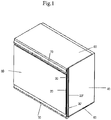
Fig. 1 : a schematic view of an ultrasonic probe according to the present invention:
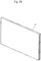
Figs. 2a to 2c : the procedures for forming two electrodes on a piezoelectric element in accordance with the present invention:
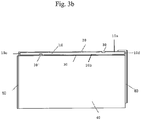
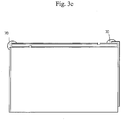
Figs. 3a to 3d : the procedure for fabricating the inventive ultrasonic probe using the assembly ofFig. 2c , in accordance with the present invention:-
Fig. 4a : the vibration characteristic of a piezoelectric element having the electrodes formed according to Example of the present invention: and -
Fig. 4b : the vibration characteristic of a piezoelectric element having the electrodes formed in Comparative Example.
-
- The inventive ultrasonic probe is characterized by comprising uniquely designed electrodes and FPCB attached thereto in a form not influenced by the paste used for the attachment.
- An ultrasonic probe conventionally contains a piezoelectric device (an ultrasonic transmitting/receiving element) comprising a piezoelectric element consisting essentially of a piezoelectric single crystal; a first and second electrodes formed on an ultrasonic wave transmitting/receiving face and the face opposite to the transmitting/receiving face of the piezoelectric element, respectively; acoustic matching layers formed on the first electrode; an acoustic lens formed to cover the entire surface of the acoustic matching layer; a ground electrode connected to the first electrode; and a flexible printed circuit board for signal, connected to the second electrode.
- The inventive ultrasonic probe is characterized in that the first electrode is formed on a substantial portion of a first main face, a first side face and a part of a second main face of the piezoelectric element, and the second electrode is formed on a substantial portion of a second main face, a second side face and a part of a first main face of the piezoelectric element, and that the two electrodes are isolated from each other by two grooves formed on the first and second main faces of the piezoelectric element, in a manner parallel to the side edges of the piezoelectric element, respectively, at positions separated from the second and first side edges by a given distance, respectively.
- The inventive ultrasonic probe may be fabricated as shown in
Figs. 2 and3 . Specifically,electrode layer 20" is deposited on the first and secondmain faces Fig. 2a ), to obtain a coated wafer (seeFig. 2b ). - The piezoelectric element may have a thickness of 20 to 500,000 µm, preferably 50 to 400 µm, in the direction of vibration.
- The electrode layer may be made of a conductive metal such as Cr, Cu, Ni, Au, etc., and a combination thereof. The deposition of the electrode layer may be conducted using a sputtering, electronic-beam, thermal-evaporation or electroplating method, and the thickness of the deposited electrode may range from 100 to 10,000 Å.
- Then, two
grooves 30, 30' are formed to separateelectrode layer 20" intofirst electrode 20 formed mainly on firstmain face 10a andfirst side face 10c (an ultrasonic wave transmitting/receiving face), and second electrode 20' formed mainly on secondmain face 10b andsecond side face 10d (the face opposite to the transmitting/receiving face), as shown inFig. 2c . - The
grooves 30, 30' may each be formed at a position separated from the side edge of the piezoelectric element by a given distance, for example a distance to make room for applying an epoxy paste to attach the electrode to a flexible printed circuit board or a ground electrode in a later step, using a dicing saw. Preferably, the grooves may be formed at the position of 1 to 1.5 mm inwardly from each side edge, and according to the invention, to a depth corresponding to 70 to 80% of the wafer thickness, in order to inhibit the generation of undesirable vibration. - The
resulting assembly 100 is then used to fabricate the inventive ultrasonic probe, as shown inFigs. 3a to 3d . -
Fig. 3a shows the step of attachingbacking layer 40 to the electrode layer deposited on secondmain face 10b of the piezoelectric element, using an epoxy paste in a conventional manner, andFig. 3b shows the step of attachingground electrode plate 50 and flexible printedcircuit board 60 for signal. - In accordance with the present invention, as represented in
Fig. 3b ,ground electrode plate 50 is attached tofirst electrode 20 atfirst side face 10c ofpiezoelectric element 10, and flexible printedcircuit board 60 is attached to second electrode 20' in the front portion of thegroove 30 positioned on firstmain face 10a of the piezoelectric element, extending fromsecond side face 10d of the piezoelectric element, and bending at the end part at a right angle. - The attachment of the ground electrode plate and the flexible printed circuit board to the first and second electrodes, respectively, may be conventionally carried out using
conductive epoxy paste 70, preferably a conductive silver epoxy paste, as shown inFig. 3c , and the use of such bended end part make the bonding of the electrode with the flexible printed circuit board strong. - Subsequently, at least one
acoustic matching layer 80 may be formed on the electrode layer deposited on the first main face of the piezoelectric element, as inFig. 3d , and thereon an acoustic lens may be covered. - The ultrasonic probe fabricated by the inventive method, as shown in
Fig. 1 , can have excellent vibration characteristics, a wide frequency band, and a high sensitivity. - The piezoelectric single crystal used in the ultrasonic probe may be any strongly ferroelectric, homogeneous single crystal, preferably PMN-PT, of which an example may have the composition of formula (I):
x(A)y(B)z(C)-p(P)n(N) (I)
wherein, - (A) is Pb(Mg1/3Nb2/3)O3 or Pb(Zn1/3Nb2/3)O3,
- (B) is PbTiO3,
- (C) is LiTaO3,
- (P) is a metal selected from the group consisting of Pt, Au, Ag, Pd and Rh,
- (N) is an oxide of a metal selected from the group consisting of Ni, Co, Fe, Sr, Sc, Ru, Cu and Cd,
- x is a number in the range of 0.65 to 0.98,
- y is a number in the range of 0.01 to 0.34,
- z is a number in the range of 0.01 to 0.1,
- p is a number in the range of 0.01 to 5, and
- n is a number in the range of 0.01 to 5.
- The single crystal of formula (I) may be prepared by way of conducting a solid phase reaction followed by melting-crystallization, by a method described in Korean Patent No.
392754 - The piezoelectric single crystal of formula (I) has a high dielectric constant of about 5,500 or higher, a piezoelectric constant of about 1,500 pC/N or higher at an ambient temperature, and a low temperature coefficient in a broad temperature range of 20 to 90°C.
- The inventive ultrasonic probe has a relative dielectric constant ranging from about 1,000 to 10,000, the velocity of a sound wave generated on the (001) face ranging from 1,200 to 4,000 m/s (frequency constant: 1,400 to 2,000 Hz.m), and a high electromechanical coefficient (k33') ranging from 80 to 95%. Accordingly, the inventive ultrasonic probe can be beneficially used for an ultrasonic diagnosis in medical, military, and industrial fields.
- The following Examples are given for the purpose of illustration only and are not intended to limit the scope of the invention.
- An ultrasonic probe as shown in
Fig. 1 , according to the present invention, was fabricated by a method comprising the procedures as shown inFigs. 2 and3 . - Piezoelectric
single crystal substrate 10 having a (001) face (surface 10a) and a size of 20-25mm x 15-20mm x 0.4-0.5mm was prepared, and metal layer (Cr/Cu/Au) 20" was deposited using a DC sputtering method on surfaces10a, 10b, 10c and 10d of the substrate (but not onsurfaces Figs. 2a and2b ). - Subsequently, two
grooves 30 and 30' were formed onsurfaces metal layer 20" into twoelectrodes 20 and 20' by using a dicing saw: Groove 30 was formed onelectrode layer 20" deposited onsurface 10a in a manner parallel to the edge formed withsurface 10d at a distance of 1-1.5 mm from said edge, while groove 30' was formed onelectrode layer 20" deposited onsurface 10b at a distance of 1-1.5 mm from the side edge withsurface 10c of the substrate (Fig. 2c ). Each of twogrooves 30, 30' had a depth of 0.25-0.35 mm. - Backing
layer 40 was laminated on the electrode layer deposited onsurface 10b ofpiezoelectric substrate 10 using an epoxy paste (Fig. 3a ), andground electrode plate 50 was attached toelectrode 20 atfirst side face 10c ofpiezoelectric substrate 10 while flexible printedcircuit board 60 was attached to electrode 20' at a part of the front ofgroove 30, beyondsecond side face 10d, ofpiezoelectric substrate 10, by bending at a right angle (Fig. 3b ). Thereafter, two acoustic matching layers 80 were laminated on the electrode layer deposited onsurface 10a ofpiezoelectric substrate 10, and thereon an acoustic lens was covered to fabricate the inventive ultrasonic probe, as shown inFig. 1 . - The procedures of Example were repeated except that the two
electrodes 20, 20' were formed by coating an electrode material after a masking tape was covered on theisolation portions 30, 30' and then removing the masking tape after coating, to fabricate an ultrasonic probe. - The vibration characteristic of the piezoelectric elements on which the electrodes were deposited according to Example and Comparative Example were tested and the results are represented in
Fig. 4a and Fig. 4b , respectively. - From
Fig. 4b , it can be seen that the piezoelectric element according to Comparative Example generates an undesirable vibration as shown in a dot-line box. In contrast,Fig. 4a shows that such undesirable vibration did not appear in the piezoelectric element according to the present invention. Accordingly, the inventive probe comprising electrodes isolated by grooves having a given depth gives improved vibration performance. - The probing characteristics (the relative sensitivity and the band-width) of the ultrasonic probes fabricated in Example and Comparative Example were measured with a pulse-echo response test, and the results are shown in Table 1.
Table 1 Probe of Example Probe of Comparative Example Relative sensitivity (dB) 1.5 0 -6dB Band width (%) 101.9 85.1 - Table 1 shows that the inventive probe having electrode isolation grooves is better in terms of sensitivity and band-width than the probe of Comparative Example having a simple isolation portion.
- While the invention has been described in connection with the above specific embodiments, it should be recognized that various modifications and changes may be made to the invention by those skilled in the art without departing from the scope of the invention as defined by the appended claims.
Claims (8)
- An ultrasonic probe comprising:(A) a piezoelectric element consisting essentially of a piezoelectric single crystal and having first and second main faces (10a, 10b) and first and second side faces (10c, 10d);(B) a first electrode (20) deposited on a substantial portion of the first main face (10a), the first side face (10c), and a part of the second main face (10b) of the piezoelectric element, and a second electrode (20') deposited on a substantial portion of the second main face (10b), the second side face (10d), and a part of the first main face (10a) of the piezoelectric element, the first and second electrodes being isolated from each other by two grooves (30, 30') formed on the first and second main faces of the piezoelectric element, in a manner parallel to the side edges of the piezoelectric element, respectively, at positions separated from the second and first side edges by a given distance, respectively;(C) a backing layer (40) attached to the electrode layer deposited on the second main face (10b) of the piezoelectric element;(D) a ground electrode (50) attached to the first electrode (20) at the first side face of the piezoelectric element; and(E) characterized by a flexible printed circuit board (60) attached to the second electrode (20') on the first main face (10a), an end part of the flexible printed circuit board (60) being attached to the second electrode (20') between the groove (30) and the second side face (10d) of the piezoelectric element, and bending to form a right angle, the flexible printed circuit board (60) extending from the second side face (10d) of the piezoelectric element,wherein the two grooves (30, 30') have a depth corresponding to 70 to 80% of the total piezoelectric element thickness.
- The ultrasonic probe of claim 1, wherein the grooves (30, 30') are positioned at a distance to make room for applying an epoxy paste to attach the electrodes to the flexible printed circuit board (60) or the ground electrode (50), inwardly from respective side edges of the piezoelectric element.
- The ultrasonic probe of claim 2, wherein the two grooves (30, 30') are positioned at 1-1.5 mm inwardly from respective side edges of the piezoelectric element.
- A method of the fabrication of an ultrasonic probe comprising:(A) depositing an electrode layer (20") on a first and second main faces (10a, 10b) and a first and second side faces (10c, 10d) of a piezoelectric element;(B) forming two grooves (30, 30') on the first and second main face (10a, 10b) of the piezoelectric element, in a manner parallel to the side edges of the piezoelectric element, respectively, at positions separated from the second and first side edges of the piezoelectric element by a given distance, respectively, to separate the electrode layer into two electrodes (20, 20');(C) attaching a backing layer (40) to the electrode layer deposited on the second main face (10b) of the piezoelectric element;(D) attaching a ground electrode (50) to the first electrode (20) at the side face of piezoelectric element; and(E) characterized by attaching a flexible printed circuit board (60) to the second electrode (20') on the first main face (10a), an end part of the flexible printed circuit board (60) being attached to the second electrode (20') between the groove (30) and the second side face (10d) of the piezoelectric element, and bending to form a right angle, the flexible printed circuit board (60) extending from the second side face (10d) of the piezoelectric element,wherein the two grooves (30, 30') are formed to have a depth corresponding to 70 to 80% of the total piezoelectric element thickness.
- The method of claim 4, wherein the two grooves (30, 30') are formed at a distance to make room for applying an epoxy paste to attach the electrodes to the flexible printed circuit board (60) or the ground electrode (50), inwardly from respective side edges of the piezoelectric element.
- The method of claim 5, wherein the two grooves (30, 30') are formed at a position of 1-1.5 mm inwardly from respective side edges of the piezoelectric element.
- The method of claim 6, wherein the epoxy paste is a silver epoxy paste.
- The method of claim 4, wherein the two grooves (30, 30') are formed using a dicing saw.
Applications Claiming Priority (1)
| Application Number | Priority Date | Filing Date | Title |
|---|---|---|---|
| PCT/KR2004/001164 WO2005110235A1 (en) | 2004-05-17 | 2004-05-17 | Ultrasonic probe and method for the fabrication thereof |
Publications (3)
| Publication Number | Publication Date |
|---|---|
| EP1765175A1 EP1765175A1 (en) | 2007-03-28 |
| EP1765175A4 EP1765175A4 (en) | 2017-07-12 |
| EP1765175B1 true EP1765175B1 (en) | 2019-01-16 |
Family
ID=35393947
Family Applications (1)
| Application Number | Title | Priority Date | Filing Date |
|---|---|---|---|
| EP04733484.2A Expired - Lifetime EP1765175B1 (en) | 2004-05-17 | 2004-05-17 | Ultrasonic probe and method for the fabrication thereof |
Country Status (4)
| Country | Link |
|---|---|
| EP (1) | EP1765175B1 (en) |
| JP (1) | JP4486127B2 (en) |
| CN (1) | CN100473353C (en) |
| WO (1) | WO2005110235A1 (en) |
Families Citing this family (2)
| Publication number | Priority date | Publication date | Assignee | Title |
|---|---|---|---|---|
| CN106446752B (en) * | 2015-08-04 | 2019-07-02 | 上海箩箕技术有限公司 | Electronic product |
| CN121125416B (en) * | 2025-11-17 | 2026-02-27 | 苏州欧伏安传感技术研究所有限公司 | Cross-metal communication methods, high-frequency ultrasonic transducers and their fabrication methods and systems |
Family Cites Families (13)
| Publication number | Priority date | Publication date | Assignee | Title |
|---|---|---|---|---|
| JPS56158648A (en) * | 1980-05-09 | 1981-12-07 | Tokyo Shibaura Electric Co | Ultrasonic diagnostic apparatus |
| KR830004828A (en) * | 1981-03-31 | 1983-07-20 | 시바 쇼오이찌 | Ultrasonic Diagnostic Device |
| JPS61112500A (en) * | 1984-11-06 | 1986-05-30 | Matsushita Electric Ind Co Ltd | Ultrasonic probe |
| DE3683509D1 (en) * | 1985-02-08 | 1992-03-05 | Matsushita Electric Industrial Co Ltd | ULTRASONIC CONVERTER. |
| JP3015481B2 (en) * | 1990-03-28 | 2000-03-06 | 株式会社東芝 | Ultrasonic probe system |
| US5423220A (en) * | 1993-01-29 | 1995-06-13 | Parallel Design | Ultrasonic transducer array and manufacturing method thereof |
| DE4427798C2 (en) * | 1993-08-06 | 1998-04-09 | Toshiba Kawasaki Kk | Piezoelectric single crystal and its use in an ultrasonic probe and ultrasonic array probe |
| US5810009A (en) * | 1994-09-27 | 1998-09-22 | Kabushiki Kaisha Toshiba | Ultrasonic probe, ultrasonic probe device having the ultrasonic probe, and method of manufacturing the ultrasonic probe |
| US5857974A (en) * | 1997-01-08 | 1999-01-12 | Endosonics Corporation | High resolution intravascular ultrasound transducer assembly having a flexible substrate |
| JP3570599B2 (en) * | 1997-01-14 | 2004-09-29 | 株式会社村田製作所 | Piezoelectric element and method of manufacturing the same |
| JP4153576B2 (en) * | 1997-11-25 | 2008-09-24 | 株式会社東芝 | Ultrasonic transducer |
| US6437487B1 (en) * | 2001-02-28 | 2002-08-20 | Acuson Corporation | Transducer array using multi-layered elements and a method of manufacture thereof |
| US20040054287A1 (en) * | 2002-08-29 | 2004-03-18 | Stephens Douglas Neil | Ultrasonic imaging devices and methods of fabrication |
-
2004
- 2004-05-17 CN CNB2004800430574A patent/CN100473353C/en not_active Expired - Lifetime
- 2004-05-17 JP JP2007526959A patent/JP4486127B2/en not_active Expired - Lifetime
- 2004-05-17 EP EP04733484.2A patent/EP1765175B1/en not_active Expired - Lifetime
- 2004-05-17 WO PCT/KR2004/001164 patent/WO2005110235A1/en not_active Ceased
Non-Patent Citations (1)
| Title |
|---|
| None * |
Also Published As
| Publication number | Publication date |
|---|---|
| CN1953710A (en) | 2007-04-25 |
| EP1765175A4 (en) | 2017-07-12 |
| EP1765175A1 (en) | 2007-03-28 |
| JP2007537818A (en) | 2007-12-27 |
| CN100473353C (en) | 2009-04-01 |
| JP4486127B2 (en) | 2010-06-23 |
| WO2005110235A1 (en) | 2005-11-24 |
Similar Documents
| Publication | Publication Date | Title |
|---|---|---|
| JP5318904B2 (en) | Multilayer ultrasonic transducer and manufacturing method thereof | |
| US9812634B2 (en) | Method of making thick film transducer arrays | |
| US6217979B1 (en) | Piezoelectric/electrostrictive film element | |
| EP1642531B1 (en) | Ultrasonic probe and ultrasonic diagnostic aparatus | |
| US5402791A (en) | Piezoelectric single crystal, ultrasonic probe, and array-type ultrasonic probe | |
| GB2052918A (en) | Piezoelectric transducers | |
| US6153967A (en) | Ultrasonic probe and ultrasonic diagnostic apparatus | |
| US6951135B2 (en) | Ultrasonic probe and method for the fabrication thereof | |
| EP1765175A1 (en) | Ultrasonic probe and method for the fabrication thereof | |
| EP1703571B1 (en) | Piezoelectric device | |
| JP3413025B2 (en) | Piezoelectric element | |
| KR100642677B1 (en) | Ultrasonic transducer and its manufacturing method | |
| JP2013026682A (en) | Medical composite single-crystal piezoelectric vibrator, medical ultrasonic probe, method of manufacturing medical composite single-crystal piezoelectric vibrator, and method of manufacturing medical ultrasonic probe | |
| JP3251727B2 (en) | Ultrasonic probe | |
| JP2000299247A (en) | Chip capacitor | |
| JPH06225391A (en) | Ultrasonic wave probe and manufacture thereof | |
| JP2001102650A (en) | Multilayer piezoelectric single crystal element, method of manufacturing multilayer piezoelectric single crystal element, and ultrasonic probe using the multilayer piezoelectric single crystal element | |
| JP2001285995A (en) | Ultrasonic probe | |
| JPS61172546A (en) | Ultrasonic probe | |
| JPH01174199A (en) | Manufacture of multi-layer ultrasonic probe | |
| HK1112659A (en) | Multilayer ultrasonic transducer and method for manufacturing same | |
| JPS6054599A (en) | Linear array type ultrasonic probe |
Legal Events
| Date | Code | Title | Description |
|---|---|---|---|
| PUAI | Public reference made under article 153(3) epc to a published international application that has entered the european phase |
Free format text: ORIGINAL CODE: 0009012 |
|
| 17P | Request for examination filed |
Effective date: 20061215 |
|
| AK | Designated contracting states |
Kind code of ref document: A1 Designated state(s): AT BE BG CH CY CZ DE DK EE ES FI FR GB GR HU IE IT LI LU MC NL PL PT RO SE SI SK TR |
|
| RIN1 | Information on inventor provided before grant (corrected) |
Inventor name: JUNG, HO Inventor name: RHIM, SUNGMINPUREUNMAEUL BYUCKSAN APT. |
|
| DAX | Request for extension of the european patent (deleted) | ||
| REG | Reference to a national code |
Ref country code: DE Ref legal event code: R079 Ref document number: 602004053641 Country of ref document: DE Free format text: PREVIOUS MAIN CLASS: A61B0008000000 Ipc: B06B0001060000 |
|
| RA4 | Supplementary search report drawn up and despatched (corrected) |
Effective date: 20170609 |
|
| RIC1 | Information provided on ipc code assigned before grant |
Ipc: B06B 1/06 20060101AFI20170602BHEP |
|
| STAA | Information on the status of an ep patent application or granted ep patent |
Free format text: STATUS: EXAMINATION IS IN PROGRESS |
|
| 17Q | First examination report despatched |
Effective date: 20180206 |
|
| GRAP | Despatch of communication of intention to grant a patent |
Free format text: ORIGINAL CODE: EPIDOSNIGR1 |
|
| STAA | Information on the status of an ep patent application or granted ep patent |
Free format text: STATUS: GRANT OF PATENT IS INTENDED |
|
| INTG | Intention to grant announced |
Effective date: 20180806 |
|
| GRAS | Grant fee paid |
Free format text: ORIGINAL CODE: EPIDOSNIGR3 |
|
| GRAA | (expected) grant |
Free format text: ORIGINAL CODE: 0009210 |
|
| STAA | Information on the status of an ep patent application or granted ep patent |
Free format text: STATUS: THE PATENT HAS BEEN GRANTED |
|
| AK | Designated contracting states |
Kind code of ref document: B1 Designated state(s): AT BE BG CH CY CZ DE DK EE ES FI FR GB GR HU IE IT LI LU MC NL PL PT RO SE SI SK TR |
|
| REG | Reference to a national code |
Ref country code: GB Ref legal event code: FG4D |
|
| REG | Reference to a national code |
Ref country code: CH Ref legal event code: EP |
|
| REG | Reference to a national code |
Ref country code: IE Ref legal event code: FG4D |
|
| REG | Reference to a national code |
Ref country code: DE Ref legal event code: R096 Ref document number: 602004053641 Country of ref document: DE |
|
| REG | Reference to a national code |
Ref country code: AT Ref legal event code: REF Ref document number: 1089304 Country of ref document: AT Kind code of ref document: T Effective date: 20190215 |
|
| REG | Reference to a national code |
Ref country code: NL Ref legal event code: MP Effective date: 20190116 |
|
| PG25 | Lapsed in a contracting state [announced via postgrant information from national office to epo] |
Ref country code: NL Free format text: LAPSE BECAUSE OF FAILURE TO SUBMIT A TRANSLATION OF THE DESCRIPTION OR TO PAY THE FEE WITHIN THE PRESCRIBED TIME-LIMIT Effective date: 20190116 |
|
| REG | Reference to a national code |
Ref country code: AT Ref legal event code: MK05 Ref document number: 1089304 Country of ref document: AT Kind code of ref document: T Effective date: 20190116 |
|
| PG25 | Lapsed in a contracting state [announced via postgrant information from national office to epo] |
Ref country code: PL Free format text: LAPSE BECAUSE OF FAILURE TO SUBMIT A TRANSLATION OF THE DESCRIPTION OR TO PAY THE FEE WITHIN THE PRESCRIBED TIME-LIMIT Effective date: 20190116 Ref country code: FI Free format text: LAPSE BECAUSE OF FAILURE TO SUBMIT A TRANSLATION OF THE DESCRIPTION OR TO PAY THE FEE WITHIN THE PRESCRIBED TIME-LIMIT Effective date: 20190116 Ref country code: PT Free format text: LAPSE BECAUSE OF FAILURE TO SUBMIT A TRANSLATION OF THE DESCRIPTION OR TO PAY THE FEE WITHIN THE PRESCRIBED TIME-LIMIT Effective date: 20190516 Ref country code: SE Free format text: LAPSE BECAUSE OF FAILURE TO SUBMIT A TRANSLATION OF THE DESCRIPTION OR TO PAY THE FEE WITHIN THE PRESCRIBED TIME-LIMIT Effective date: 20190116 Ref country code: ES Free format text: LAPSE BECAUSE OF FAILURE TO SUBMIT A TRANSLATION OF THE DESCRIPTION OR TO PAY THE FEE WITHIN THE PRESCRIBED TIME-LIMIT Effective date: 20190116 |
|
| PG25 | Lapsed in a contracting state [announced via postgrant information from national office to epo] |
Ref country code: BG Free format text: LAPSE BECAUSE OF FAILURE TO SUBMIT A TRANSLATION OF THE DESCRIPTION OR TO PAY THE FEE WITHIN THE PRESCRIBED TIME-LIMIT Effective date: 20190416 Ref country code: GR Free format text: LAPSE BECAUSE OF FAILURE TO SUBMIT A TRANSLATION OF THE DESCRIPTION OR TO PAY THE FEE WITHIN THE PRESCRIBED TIME-LIMIT Effective date: 20190417 |
|
| REG | Reference to a national code |
Ref country code: DE Ref legal event code: R097 Ref document number: 602004053641 Country of ref document: DE |
|
| PG25 | Lapsed in a contracting state [announced via postgrant information from national office to epo] |
Ref country code: AT Free format text: LAPSE BECAUSE OF FAILURE TO SUBMIT A TRANSLATION OF THE DESCRIPTION OR TO PAY THE FEE WITHIN THE PRESCRIBED TIME-LIMIT Effective date: 20190116 Ref country code: IT Free format text: LAPSE BECAUSE OF FAILURE TO SUBMIT A TRANSLATION OF THE DESCRIPTION OR TO PAY THE FEE WITHIN THE PRESCRIBED TIME-LIMIT Effective date: 20190116 Ref country code: DK Free format text: LAPSE BECAUSE OF FAILURE TO SUBMIT A TRANSLATION OF THE DESCRIPTION OR TO PAY THE FEE WITHIN THE PRESCRIBED TIME-LIMIT Effective date: 20190116 Ref country code: EE Free format text: LAPSE BECAUSE OF FAILURE TO SUBMIT A TRANSLATION OF THE DESCRIPTION OR TO PAY THE FEE WITHIN THE PRESCRIBED TIME-LIMIT Effective date: 20190116 Ref country code: RO Free format text: LAPSE BECAUSE OF FAILURE TO SUBMIT A TRANSLATION OF THE DESCRIPTION OR TO PAY THE FEE WITHIN THE PRESCRIBED TIME-LIMIT Effective date: 20190116 Ref country code: SK Free format text: LAPSE BECAUSE OF FAILURE TO SUBMIT A TRANSLATION OF THE DESCRIPTION OR TO PAY THE FEE WITHIN THE PRESCRIBED TIME-LIMIT Effective date: 20190116 Ref country code: CZ Free format text: LAPSE BECAUSE OF FAILURE TO SUBMIT A TRANSLATION OF THE DESCRIPTION OR TO PAY THE FEE WITHIN THE PRESCRIBED TIME-LIMIT Effective date: 20190116 |
|
| PLBE | No opposition filed within time limit |
Free format text: ORIGINAL CODE: 0009261 |
|
| STAA | Information on the status of an ep patent application or granted ep patent |
Free format text: STATUS: NO OPPOSITION FILED WITHIN TIME LIMIT |
|
| 26N | No opposition filed |
Effective date: 20191017 |
|
| REG | Reference to a national code |
Ref country code: CH Ref legal event code: PL |
|
| PG25 | Lapsed in a contracting state [announced via postgrant information from national office to epo] |
Ref country code: CH Free format text: LAPSE BECAUSE OF NON-PAYMENT OF DUE FEES Effective date: 20190531 Ref country code: LI Free format text: LAPSE BECAUSE OF NON-PAYMENT OF DUE FEES Effective date: 20190531 Ref country code: MC Free format text: LAPSE BECAUSE OF FAILURE TO SUBMIT A TRANSLATION OF THE DESCRIPTION OR TO PAY THE FEE WITHIN THE PRESCRIBED TIME-LIMIT Effective date: 20190116 |
|
| REG | Reference to a national code |
Ref country code: BE Ref legal event code: MM Effective date: 20190531 |
|
| PG25 | Lapsed in a contracting state [announced via postgrant information from national office to epo] |
Ref country code: LU Free format text: LAPSE BECAUSE OF NON-PAYMENT OF DUE FEES Effective date: 20190517 Ref country code: SI Free format text: LAPSE BECAUSE OF FAILURE TO SUBMIT A TRANSLATION OF THE DESCRIPTION OR TO PAY THE FEE WITHIN THE PRESCRIBED TIME-LIMIT Effective date: 20190116 |
|
| PG25 | Lapsed in a contracting state [announced via postgrant information from national office to epo] |
Ref country code: TR Free format text: LAPSE BECAUSE OF FAILURE TO SUBMIT A TRANSLATION OF THE DESCRIPTION OR TO PAY THE FEE WITHIN THE PRESCRIBED TIME-LIMIT Effective date: 20190116 |
|
| PG25 | Lapsed in a contracting state [announced via postgrant information from national office to epo] |
Ref country code: IE Free format text: LAPSE BECAUSE OF NON-PAYMENT OF DUE FEES Effective date: 20190517 |
|
| PG25 | Lapsed in a contracting state [announced via postgrant information from national office to epo] |
Ref country code: BE Free format text: LAPSE BECAUSE OF NON-PAYMENT OF DUE FEES Effective date: 20190531 |
|
| PG25 | Lapsed in a contracting state [announced via postgrant information from national office to epo] |
Ref country code: CY Free format text: LAPSE BECAUSE OF FAILURE TO SUBMIT A TRANSLATION OF THE DESCRIPTION OR TO PAY THE FEE WITHIN THE PRESCRIBED TIME-LIMIT Effective date: 20190116 |
|
| PG25 | Lapsed in a contracting state [announced via postgrant information from national office to epo] |
Ref country code: HU Free format text: LAPSE BECAUSE OF FAILURE TO SUBMIT A TRANSLATION OF THE DESCRIPTION OR TO PAY THE FEE WITHIN THE PRESCRIBED TIME-LIMIT; INVALID AB INITIO Effective date: 20040517 |
|
| PGFP | Annual fee paid to national office [announced via postgrant information from national office to epo] |
Ref country code: FR Payment date: 20230523 Year of fee payment: 20 Ref country code: DE Payment date: 20230526 Year of fee payment: 20 |
|
| PGFP | Annual fee paid to national office [announced via postgrant information from national office to epo] |
Ref country code: GB Payment date: 20230526 Year of fee payment: 20 |
|
| REG | Reference to a national code |
Ref country code: DE Ref legal event code: R071 Ref document number: 602004053641 Country of ref document: DE |
|
| REG | Reference to a national code |
Ref country code: GB Ref legal event code: PE20 Expiry date: 20240516 |
|
| PG25 | Lapsed in a contracting state [announced via postgrant information from national office to epo] |
Ref country code: GB Free format text: LAPSE BECAUSE OF EXPIRATION OF PROTECTION Effective date: 20240516 |
|
| PG25 | Lapsed in a contracting state [announced via postgrant information from national office to epo] |
Ref country code: GB Free format text: LAPSE BECAUSE OF EXPIRATION OF PROTECTION Effective date: 20240516 |