EP1763059A2 - Image display apparatus - Google Patents
Image display apparatus Download PDFInfo
- Publication number
- EP1763059A2 EP1763059A2 EP06010143A EP06010143A EP1763059A2 EP 1763059 A2 EP1763059 A2 EP 1763059A2 EP 06010143 A EP06010143 A EP 06010143A EP 06010143 A EP06010143 A EP 06010143A EP 1763059 A2 EP1763059 A2 EP 1763059A2
- Authority
- EP
- European Patent Office
- Prior art keywords
- image display
- display apparatus
- fluorescent layer
- electron
- supporting member
- Prior art date
- Legal status (The legal status is an assumption and is not a legal conclusion. Google has not performed a legal analysis and makes no representation as to the accuracy of the status listed.)
- Withdrawn
Links
- 239000000758 substrate Substances 0.000 claims abstract description 21
- 238000010894 electron beam technology Methods 0.000 claims description 57
- 239000011159 matrix material Substances 0.000 claims description 4
- 239000012212 insulator Substances 0.000 claims 1
- 238000010276 construction Methods 0.000 description 35
- 239000011295 pitch Substances 0.000 description 11
- 238000006073 displacement reaction Methods 0.000 description 10
- 239000011521 glass Substances 0.000 description 10
- 230000005684 electric field Effects 0.000 description 8
- 239000000126 substance Substances 0.000 description 6
- 239000004973 liquid crystal related substance Substances 0.000 description 4
- 238000000034 method Methods 0.000 description 4
- 239000010409 thin film Substances 0.000 description 3
- OKTJSMMVPCPJKN-UHFFFAOYSA-N Carbon Chemical compound [C] OKTJSMMVPCPJKN-UHFFFAOYSA-N 0.000 description 2
- 239000011248 coating agent Substances 0.000 description 2
- 238000000576 coating method Methods 0.000 description 2
- 238000007796 conventional method Methods 0.000 description 2
- 238000005336 cracking Methods 0.000 description 2
- 229910003460 diamond Inorganic materials 0.000 description 2
- 239000010432 diamond Substances 0.000 description 2
- 238000004519 manufacturing process Methods 0.000 description 2
- 239000000463 material Substances 0.000 description 2
- XOLBLPGZBRYERU-UHFFFAOYSA-N tin dioxide Chemical compound O=[Sn]=O XOLBLPGZBRYERU-UHFFFAOYSA-N 0.000 description 2
- 239000013598 vector Substances 0.000 description 2
- 230000000007 visual effect Effects 0.000 description 2
- 230000001133 acceleration Effects 0.000 description 1
- 230000002411 adverse Effects 0.000 description 1
- 229910052799 carbon Inorganic materials 0.000 description 1
- 239000003575 carbonaceous material Substances 0.000 description 1
- 238000006243 chemical reaction Methods 0.000 description 1
- 230000003247 decreasing effect Effects 0.000 description 1
- 230000000694 effects Effects 0.000 description 1
- 230000005611 electricity Effects 0.000 description 1
- 229910002804 graphite Inorganic materials 0.000 description 1
- 239000010439 graphite Substances 0.000 description 1
- 238000000206 photolithography Methods 0.000 description 1
- 238000007639 printing Methods 0.000 description 1
- 239000011347 resin Substances 0.000 description 1
- 229920005989 resin Polymers 0.000 description 1
- 238000007789 sealing Methods 0.000 description 1
- 238000007493 shaping process Methods 0.000 description 1
- 230000002269 spontaneous effect Effects 0.000 description 1
- 239000012780 transparent material Substances 0.000 description 1
Images


Classifications
-
- H—ELECTRICITY
- H01—ELECTRIC ELEMENTS
- H01J—ELECTRIC DISCHARGE TUBES OR DISCHARGE LAMPS
- H01J31/00—Cathode ray tubes; Electron beam tubes
- H01J31/08—Cathode ray tubes; Electron beam tubes having a screen on or from which an image or pattern is formed, picked up, converted, or stored
- H01J31/10—Image or pattern display tubes, i.e. having electrical input and optical output; Flying-spot tubes for scanning purposes
- H01J31/12—Image or pattern display tubes, i.e. having electrical input and optical output; Flying-spot tubes for scanning purposes with luminescent screen
- H01J31/123—Flat display tubes
-
- H—ELECTRICITY
- H01—ELECTRIC ELEMENTS
- H01J—ELECTRIC DISCHARGE TUBES OR DISCHARGE LAMPS
- H01J29/00—Details of cathode-ray tubes or of electron-beam tubes of the types covered by group H01J31/00
- H01J29/02—Electrodes; Screens; Mounting, supporting, spacing or insulating thereof
- H01J29/028—Mounting or supporting arrangements for flat panel cathode ray tubes, e.g. spacers particularly relating to electrodes
-
- H—ELECTRICITY
- H01—ELECTRIC ELEMENTS
- H01J—ELECTRIC DISCHARGE TUBES OR DISCHARGE LAMPS
- H01J29/00—Details of cathode-ray tubes or of electron-beam tubes of the types covered by group H01J31/00
- H01J29/46—Arrangements of electrodes and associated parts for generating or controlling the ray or beam, e.g. electron-optical arrangement
- H01J29/467—Control electrodes for flat display tubes, e.g. of the type covered by group H01J31/123
-
- H—ELECTRICITY
- H01—ELECTRIC ELEMENTS
- H01J—ELECTRIC DISCHARGE TUBES OR DISCHARGE LAMPS
- H01J29/00—Details of cathode-ray tubes or of electron-beam tubes of the types covered by group H01J31/00
- H01J29/86—Vessels; Containers; Vacuum locks
- H01J29/864—Spacers between faceplate and backplate of flat panel cathode ray tubes
-
- H—ELECTRICITY
- H01—ELECTRIC ELEMENTS
- H01J—ELECTRIC DISCHARGE TUBES OR DISCHARGE LAMPS
- H01J2329/00—Electron emission display panels, e.g. field emission display panels
- H01J2329/86—Vessels
- H01J2329/8625—Spacing members
Definitions
- the present invention relates to an image display apparatus, and more particularly, relates to a thin image display apparatus used for a video camera and the like.
- cathode ray tubes mainly have been used as image display apparatuses for color televisions, personal computers and the like.
- image display apparatuses have been required to be miniaturized and made lighter and thinner.
- various types of thin image display apparatuses have been developed and commercialized.
- liquid crystal displays and plasma displays have been developed actively.
- the liquid crystal displays have been applied to various types of products such as portable computers, portable televisions, video cameras, car-navigation systems and the like.
- Plasma displays have been used for products such as large-scale displays, for example, 20-inch-displays or 40-inch-displays.
- a liquid crystal display has a narrow visual angle and a slow response.
- a plasma display only high brightness is obtainable and the consumed electricity is large.
- an image display apparatus (hereinafter referred to as "a field emission image display apparatus” or “an image display apparatus") to which field emission, that is, a phenomenon in which electrons are emitted in a vacuum at room temperature, is applied, has attracted considerable attention.
- the field emission image display apparatus is of a spontaneous luminescent type, and therefore it is possible to obtain a wide visual angle and high brightness.
- its basic principle to illuminate a fluorescent substance with electron beams
- images with natural color and high reproduction can be displayed.
- Tokkai-Hei 3-149728 discloses an example of such a field emission image display apparatus.
- the field emission image display apparatus that is driven under a vacuum condition from 1 ⁇ 10 -7 to 1 ⁇ 10 -8 torr should be produced generally by vacuum-sealing the inner part. Therefore, the thin field emission image display apparatus should have a structure to be resistant to the atmospheric pressure.
- Tokkai Hei 3-149728 discloses a technique for providing a supporting member to the inner part of a field emission image display apparatus.
- FIG. 12 is a schematic cross-sectional view showing a field emission image display apparatus according to a conventional technique.
- the field emission image display apparatus shown in FIG. 12 comprises an electron emission source 101 comprising an insulating substrate 101a provided thereon with plural electron sources 101 b, a fluorescent layer 102 formed on the inner surface of the image display apparatus's panel to face the electron emission source 101, and supporting members 103 provided between the electron emission source 101 and fluorescent layer 102.
- the supporting members 103 are provided uniformly on the electron emission source 101 in order to prevent damage caused by outside pressure applied to the panel in the area between the electron emission source 101 and the fluorescent layer 102.
- FIG. 13 is a schematic cross-sectional view showing another conventional field emission image display apparatus.
- this field emission image display apparatus comprises an electron emission source 201 comprising an insulating substrate 201a provided thereon with plural electron sources 201b, a fluorescent layer 202 and supporting members 203 formed between the electron emission source 201 and the fluorescent layer 202.
- the supporting members 203 are uniformly formed on the electron emission source 201 in order to prevent damage caused by the outside pressure applied to the panel in the area between the electron emission source 201 and the fluorescent layer 202.
- This image display apparatus is distinguishable from the former one in that the supporting members 203 composing the field emission image display apparatus in FIG. 13 are negatively charged while the supporting members 103 composing the field emission image display apparatus in FIG. 12 are positively charged.
- An image display apparatus shown in FIG. 12 or 13 comprises the supporting members (103, 203) between the electron emission source (101, 201) and the fluorescent layer (102, 202), so that the field emission image display apparatus has a structure resistant to the atmospheric pressure. Electron beams (104, 204) are emitted from the electron sources (101b, 201b) formed with equal spacing on the insulating substrate (101a, 201a) and landed on predetermined positions of the fluorescent layer (102, 202), so that various images are displayed on the field emission image display apparatus. Various members required other than the above-identified ones for forming a field emission image display apparatus are omitted in FIGs. 12 and 13.
- the electron beams 104 emitted at an equal spacing will bend toward the supporting members 103 since the supporting members 103 are positively charged, and thus, the final landing positions of the electron beams 104 will not be spaced equally on the fluorescent layer 102.
- the electron beams 204 emitted at an equal spacing will bend away from the supporting members 203 since the supporting members 203 are negatively charged, and thus, the final landing positions of the electron beams 204 will not be spaced equally on the fluorescent layer 202.
- the electron beams (104, 204) are deviated from the landing positions on the fluorescent layers (102, 202), and good images are difficult to obtain.
- the supporting members (103, 203) composing the field emission image display apparatus have a predetermined thickness at the positions contacting with the fluorescent layer (102, 202). When this thickness exceeds a limit, it will be recognized as a horizontal line by someone watching the displayed images and the quality of the display images will be greatly lowered.
- plural supporting members (103, 203) are provided between the electron emission source (101, 201) and the fluorescent layer (102, 202). If the supporting members (103, 203) have different lengths, outside pressure will be applied only to the longer supporting members contacting with the fluorescent layer (102, 202), which may result in distortion or damage for the image display apparatuses.
- this invention aims to provide an image .display apparatus having a structure resistant to the atmospheric pressure by providing a supporting member to the inner part of the image display apparatus, and that will not negatively affect the image, so that good images are provided.
- an image display apparatus of this invention comprises a fluorescent layer formed on the inner surface of a vacuum container whose interior is kept under vacuum, an electron emission source comprising an insulating substrate provided with electron sources arranged thereon, and a supporting member sandwiched between the fluorescent layer and the electron emission source.
- a displacement preventing system is provided inside the image display apparatus in order to prevent displacement of the electron beams emitted from the electron sources caused by the charging of the supporting member.
- the electron beams are not displaced by the charging of the supporting member, and thus, the images will not be negatively affected by forming the supporting member.
- an image display apparatus that has a structure resistant to the atmospheric pressure and displays a good image can be obtained.
- the displacement preventing system comprises a conductive portion that is formed at a part of the supporting member near the fluorescent layer and contacts with the same layer.
- the supporting member contacting with the fluorescent layer is the conductive portion and thus it is not charged, so that the electron beams will not be affected by the electric field in the vicinity of the fluorescent layer. As a result, displacement of the electron beams caused by the charged supporting member can be prevented efficiently.
- the supporting member preferably has an electrode portion at the conductive portion opposite to the fluorescent layer and the electrode portion contacts with the conductive portion.
- the electrode portion can function as a divergent lens for the electron beams, so that the electron beams emitted from a position sufficiently separated from the supporting member can be deflected toward the supporting member.
- the electron beams are deflected toward the supporting member by using the electrode portion functioning as a divergent lens even if the electron sources sandwiching a formed supporting member are required to be arranged with more spacing compared to the other electron sources, so that the electron beams can be landed on the fluorescent layer with an equal pitch.
- the supporting member preferably has an insulating portion between the electron emission source and the electrode portion.
- the fluorescent layer can be insulated electrically from the electron emission source with certainty. As the insulating portion is charged, it may deflect the electron beams. In order to prevent the deflection, the electron sources should be separated sufficiently from the supporting member depending on the deflection degree. In the preferable construction of this invention, however, the electron beams can be deflected toward the supporting member by using the electrode portion as a divergent lens as mentioned above. In addition, the area in the vicinity of the fluorescent layer provided with the conductive portion will not be affected by the electric field. As a result, the electron beams can be landed with an equal pitch on the fluorescent layer by properly controlling some factors such as the positions of the electron sources and of the electrode portion. As a result, continuous images with no influence of the supporting member can be displayed on the image display screen.
- the electron sources are arranged on the insulating substrate so that the electron beams emitted from the electron sources are landed on the fluorescent layer with an equal pitch.
- the displacement preventing system prevents the electron beams from being displaced by the charging of the supporting member, and the electron sources can be arranged so that the electron beams will be landed with an equal pitch on the fluorescent layer by taking some factors such as the construction of the supporting member into consideration. As a result, good images free from the influence of the supporting member can be displayed.
- the electrode portion is formed wider than the insulating portion.
- the area in the vicinity of the fluorescent layer will be still less affected by the electric field, and thus, a no-electric field region can be formed with certainty in the vicinity of the fluorescent layer.
- the function of the divergent lens formed by the electrode portion can be further increased. As a result, the electron beams can be landed on the fluorescent layer with an equal pitch in a relatively simple manner, and good images can be displayed.
- a second electrode portion is provided at a part of the insulating portion near the electron emission source and the second electrode portion is wider than the insulating portion.
- the electron beam accelerating field can be kept constant at a position separated from the insulating portion.
- the electron beams can be separated sufficiently from the supporting member so that the charging of the supporting member (the insulating portion) caused by the electron beams can be minimized.
- the extension of the initial speed of the electron beams, the vectors of the initial speed of the electron beams etc. can be controlled by independently controlling the voltage applied to the respective second electrode portions, so that the disorder in uniformity of the image displayed in the vicinity of the supporting member can be controlled while observing the images. Therefore, the deviation of the beam landing caused by the deviation of the electron sources (deviations caused by manufacturing error etc.) can be corrected in a simple manner. As a result, the electron beams can be landed on the fluorescent layer with an equal pitch in a comparatively simple manner.
- the conductive portion is tapered and a part of the conductive portion contacting with the fluorescent layer is shaped narrower than the opposite part.
- the conductive portion composing the supporting member is tapered, it is possible to minimize the chance that those who observe the displayed image will recognize the part at which the conductive portions and fluorescent layer are contacted with each other.
- the image display apparatus of this invention can provide good images without shielding the display image.
- the electrode portion is resilient.
- the electrode portions can compensate the variation in length of the portions composing the supporting members other than the electrode portions.
- the conductive portions are resilient.
- the conductive portions can compensate the variation in length of the portions composing the supporting members other than the conducting portions.
- the insulating portions are resilient.
- the insulating portions can compensate the variation in length of the portions composing.the supporting members other than the insulating portions.
- the supporting members are arranged with a higher density at the center of the image display apparatus screen.
- the portion at the center of the screen, on which stress caused by the atmospheric pressure is focused can be supported with certainty, and an image display apparatus having a thin and large screen can be provided.
- An image display apparatus of this invention comprises a fluorescent layer formed on the inner surface of a vacuum container whose interior is kept under vacuum, an electron emission source having an insulating substrate provided with electron sources arranged thereon, and a supporting member sandwiched between the fluorescent layer and the electron emission source, in which the supporting member comprises a conducting portion to contact with the fluorescent layer.
- the supporting member contacting with the fluorescent layer is a conductive portion and will not be charged, so that the electron beams will not be affected by the electric field in the vicinity of the fluorescent layer. Therefore, the electron.beams are effectively prevented from displacement caused by the charging of the supporting member.
- providing supporting members will not adversely affect the images, and thus, an image display apparatus having a structure resistant to the atmospheric pressure and providing a good image display can be obtained.
- FIG. 1 is a perspective exploded view showing an image display apparatus in the first embodiment of this invention.
- FIG. 2 is a cross-sectional view showing the schematic construction of the image display apparatus of FIG. 1.
- an image display apparatus in this embodiment comprises an electron emission source 1 formed by arranging plural electron sources 1b in a matrix on an insulating substrate 1a, a fluorescent layer 2 formed on the inner surface of a panel 5, that displays an image by being excited by electron beams 4 emitted from the electron sources 1b, and supporting members 3 formed between the electron emission source 1 and the fluorescent layer 2.
- This image display apparatus is provided with a displacement preventing system (conductive portions 3a) to prevent displacement of the electron beams 4 emitted from the electron sources 1b caused by the charging of a supporting member 3.
- a vacuum container is formed from the insulating substrate 1a and a panel 5, and the inside of the image display apparatus is kept under a vacuum of about 10 -6 to 10 -8 torr.
- the fluorescent layer 2 in this embodiment is formed on the inner surface (vacuum side) of the panel plate member 5a by providing the plate-like panel image display screen (panel plate member 5a) and the surrounding wall portion (panel frame member 5b)as separate pieces.
- the plate-like panel image display screen (panel plate member 5a), the surrounding wall (panel frame member 5b) and the insulating substrate 1a are stuck together at the same time so that the vacuum container for the image display apparatus is formed.
- an electron emission source 1 can be used as long as it can emit electron beams 4 in a matrix.
- an electron emission source which is composed of a surface conductive element composed of a thin film of SnO 2 (Sb) or a thin film of Au and the like or a thin film of other materials, a microchip type electric field electron mission element such as Spindt type (microchip cathode of field emission type invented by Spindt), an electric field electron emission element having a MIN type structure or a similar structure or a cold cathode ray element composed of an electron emission material which is a carbon material such as diamond, graphite, DLC (Diamond Like Carbon) and the like, may be used.
- the electron sources 1b are arranged at a predetermined spacing on the insulating substrate 1a so that the respective electron beams 4 emitted from the respective electron sources 1b will be landed with an equal pitch on the fluorescent layer 2. In order to leave the space for the supporting members 3, larger spacing is provided between the electrode sources 1b at the positions to sandwich the supporting members 3 compared to the other positions in the insulating substrate 1a.
- the fluorescent layer 2 is formed by applying (e.g., coating) a fluorescent substance on the inner surface of the panel.
- the fluorescent substance emits light by being irradiated with electron beams emitted from the electron emission source 1.
- the fluorescent substance is coated in numerous strips on the panel inner surface in order of, for instance, red (R), green (G), and blue(B).
- the stripe-arranged fluorescent substance can be provided by some methods such as photolithography as in a usual case for forming a fluorescent surface for a cathode ray tube, or a screen-stencil.
- the glass panel 5 may have a box-shape in which the plate-like panel image display screen is incorporated with the surrounding wall portion.
- a fluorescent surface a fluorescent layer 2
- the wall portion surrounding the panel will be an obstacle in the printing step.
- a supporting member 3 comprises a conductive portion 3a as a displacement preventing system, an electrode portion 3b to direct the electron beams 4 to the predetermined positions on the fluorescent layer 2, and an insulating portion 3c to insulate the electron emission source 1 from the electrode portion 3b.
- the supporting member 3 is composed by connecting the conductive portion 3a and the insulating portion 3c via the electrode portion 3b, and formed between the electron emission source 1 and the fluorescent layer 2 so that the conductive portion 3a will contact with the fluorescent layer 2 while the insulating portion 3c will contact with the electron emission source 1.
- the glass panel 5 is made of a transparent material such as glass, since it is required that light emitted from a fluorescent layer to be observed from outside of the glass panel 5 in order to function as an image display apparatus. However, it is not required that the whole surface of the glass panel be transparent, but only the part of the glass panel 5 which contacts with the fluorescent layer 2 is transparent (in FIG. 1, the panel plate member 5a, and in FIG. 3, the upper area with largest surface). According to the construction, the image display apparatus of this invention can resist the outside pressure sufficiently even if the glass panel is not so thick. As a result, the image display apparatus can be made lighter while having a flat structure.
- FIG. 2 is a cross-sectional view showing the schematic construction of the image display apparatus of FIG. 1.
- electron beams 4 are emitted appropriately from respective electron sources 1b composing the electron emission source 1.
- Each electron beam 4 is landed at the predetermined position on the fluorescent layer 2, and various images are displayed on the image display apparatus.
- the following is an explanation about the operation and effects of the image display apparatus in this embodiment, referring to FIG. 2.
- a supporting member 3 composing the image display apparatus in this embodiment is sandwiched between the electron emission source 1 and the fluorescent layer 2 so that the conductive portion 3 a will contact with the fluorescent layer 2 while the insulating portion 3c will contact with the electron emission source 1.
- the conductive portion 3a composes the supporting portion 3 at the part near the fluorescent layer 2, the potential is equal at the fluorescent layer 2, the conductive portion 3a and the electrode portion 3b, and the supporting member 3 (conductive portion 3a) will not be charged in the vicinity of the fluorescent layer 2. Therefore, the electron beams 4 will not be affected by the electric field in the vicinity of the fluorescent layer 2.
- the electron sources 1b to sandwich each supporting member 3 are arranged to be separated from the supporting member 3 as much as possible so that the electron beams will be protected from the influence of the charged insulating portion 3c.
- the electrode portion 3b composing the supporting member 3 functions as a divergent lens to the electrode beams 4, and thus, the emitted electron beams can be deflected to the supporting member even if the electron sources 1b are arranged at the positions separated from the charged insulating portion 3c.
- the image display apparatus of this embodiment can land the electron beams on the fluorescent layer with an equal pitch by appropriately controlling the positions of the electron sources 1b arranged on the insulating substrate 1a and the positions of the electrode portions 3b composing the supporting members 3. Therefore, continuous picture images free from influences by the supporting members 3 can be displayed on the image screen.
- FIG. 4 is a cross-sectional view showing the schematic construction of an image display apparatus in the second embodiment.
- the basic construction of a display of the embodiment is the same as that of the first embodiment, except that the structure of the supporting members and the arrangement of the electrode sources are distinguishable from the first embodiment.
- a supporting member 13 composing the image display apparatus in this embodiment comprises a conductive portion 13a, an electrode portion 13b and an insulating portion 13c.
- the supporting member 13 is formed by connecting the conductive portion 13a and the insulating portion 13c via the electrode portion 13b, and sandwiched between the electron emission source 11 and the fluorescent layer 12 so that the conductive portion 13a will contact with the fluorescent layer 12 while the insulating portion 13c will contact with the electron emission source 11.
- the electrode portion 13b of this embodiment is formed to project in the direction parallel to the image display screen.
- the thus formed electrode portion 13b has a ribbon-shape when viewed from above.
- the electrode portion 13b made wider, apertures through which the electron beams 14 pass (the spacing between adjacent electrode portions 13b) become small, and the spacing of the electron sources 11b arranged on the insulating substrate 11a is controlled to correspond to the spacing between the electrode portions 13b. More specifically, the electron sources 11b sandwiching the supporting members 13 are arranged to be further separated from the supporting members 13 compared to the case of the first embodiment.
- the area in the vicinity of the fluorescent layer 12 will be less affected by the electric field present in the vicinity of the electron emission source 11, so that a no-electric field region in the vicinity of the fluorescent layer 12 can be provided with further certainty. It can also increase the function of the divergent lens formed by the electrode portion 13b, and the influence of the (charged) insulating portion 13c on the electron beams 14 can be further decreased compared to the first embodiment.
- the electron beams 14 can be landed with an equal pitch on the fluorescent layer 12 in a relatively simple manner by appropriately controlling some factors such as the positions of the electron sources 1 1b arranged on the insulating substrate 11a, and the positions and size of the electrode portion 13b composing the supporting members 13. Therefore, good images can be obtained in the image display apparatus of this embodiment.
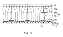
- FIG. 5 is a cross-sectional view showing the schematic construction of an image display apparatus in the third embodiment.
- the basic construction of the image display apparatus in this embodiment is the same as that of the second embodiment, except that the structure of the supporting members is distinguishable from the second embodiment.
- a supporting member 23 composing the image display apparatus in this embodiment comprises a conductive portion 23a, a first electrode portion 23b, an insulating portion 23c, and a second electrode portion 23d.
- a first electrode portion 23b is formed between the conductive portion 23a and the insulating portion 23c while the second electrode portion 23d is formed at a part of the insulating portion 23c near the electron emission source 21.
- the first and second electrode portions (23b, 23d) are formed wider than the insulating portion 23c.
- the second electrode portion 23d is basically applied with a predetermined voltage in the range from the anode voltage applied to the fluorescent layer to the voltage at the electron emission source 21 (generally 0V). Voltage can be applied independently to each second electrode portion 23d formed at each supporting member 23.
- the electron beam acceleration field can be kept constant at a position separated from the insulating portion 23c.
- charging of the supporting member 23 (insulating portion 23c) caused by the electron beams 24 can be minimized.
- the raster pitches can be controlled while observing the images. That is, the deviation of the beam landing caused by the deviation of the electron sources 21b (deviation caused by manufacturing errors or the like) can be corrected easily.
- the electron beams 24 can be landed with an equal pitch on the fluorescent layer 22 in a relatively simple manner by controlling some factors such as the positions of the electron sources 21b arranged on the insulating substrate 21a, the portions and size of the electrode portions 23b and 23d composing the supporting member 23, and the voltage applied to the second electrode portions 23d in an appropriate manner. Therefore, good images can be obtained in the image display apparatus of this embodiment.
- FIG. 6 is a cross-sectional view showing the schematic construction of an image display apparatus in the fourth embodiment.
- the basic construction of a display of the embodiment is the same as that of the first embodiment, except that the structure of the supporting members is distinguishable from that of the first embodiment.
- a supporting member 33 composing the image display apparatus in this embodiment comprises a conductive portion 33a, an electrode portion 33b and an insulating portion 33c.
- the supporting member 33 is formed by connecting the conductive portion 33a and the insulating portion 33c via the electrode portion 33b, and sandwiched between the electron emission source 31 and the fluorescent layer 32 so that the conductive portion 33a will contact with the fluorescent layer 32 while the insulating portion 33c will contact with the electron emission source 31.
- the conductive portion 33a in this embodiment is tapered, that is, this conductive portion 33a is shaped thinner at the fluorescent layer 32 side than at the electrode portion 33b side.
- numeral 31a is an insulating substrate
- 31b is an electron source
- 34 is an electron beam.
- an image display apparatus comprising conventional supporting members
- high strength for the supporting members is not required to resist the outside pressure.
- the part of a supporting member to contact with the fluorescent layer can be made very small, so that the supporting member will not disturb the image display.
- the stress caused by the outside pressure applied to the panel center is increased as the image display apparatus becomes big, and the image display apparatus should have supporting members with strength to resist the outside pressure.
- the supporting member can have quite large cross-section at the electron emission source side, while the cross-section is limited at the fluorescent layer side when considering the influences on the displayed images.
- the image display apparatus of this invention aims to solve such a problem.
- an image display apparatus of this embodiment can minimize the no-image display parts generated at the point where the conductive portion 33a contacts with the fluorescent layer 32, since the conductive portion 33a composing the supporting member 33 is tapered. As a result, good images can be obtained in the image display apparatus of this embodiment.
- An image display apparatus in this embodiment basically has the same construction as that of the fourth embodiment, except for the structure of the supporting members. More specifically, only the construction of the electrode portion is different from that of the fourth embodiment.
- the electrode portion in this embodiment has the same construction as the electrode portion 13b composing the supporting member 13 in the second embodiment referring to FIG. 4.
- the supporting member in this embodiment comprises an electrode portion having the same structure as the electrode portion 13b in the second embodiment, a conductive portion having the same structure as the conductive portion 33a in the fourth embodiment, and an insulating portion having the same structure as the insulating portion 33c in the fourth embodiment. Therefore, this embodiment can provide an image display apparatus possessing the respective advantages of the second and fourth embodiments.
- FIG. 7 is a cross-sectional view showing the schematic construction of an image display apparatus in the sixth embodiment.
- the image display apparatus in this embodiment basically has the same construction as that in the fifth embodiment, except that the structure of the supporting members is somewhat different, that is, the image display apparatus is formed by using resilient supporting members 53. More specifically, the image display apparatus in this embodiment is different from the fifth embodiment only in the structure of electrode portions 53b composing the supporting members 53.
- An electrode portion 53b composing a supporting member 53 in the embodiment comprises a first electrode component 53b 1 contacting with a tapered conductive portion 53a, and a second electrode component 53b 2 contacting with an insulating portion 53c.
- the electrode portion 53b is a trapezoid whose side lines are equal when viewed in the cross section, and it is formed by deforming to some extent at least one of the electrode components in order to provide a predetermined space between the first electrode component 53b 1 and second electrode component 53b 2 and sticking the first and second electrode components (53b 1 and 53b 2 ) together.
- the first electrode component 53b 1 is deformed to have a predetermined shape before sticking the flat second electrode component 53b 2 to this first electrode component 53b 1 , so that an electrode portion 53b having a predetermined space between the first electrode component 53b 1 and the second electrode portion 53b 2 is formed.
- the electrode portion 53b has a predetermined space as mentioned above, and the first electrode component 53b 1 has flexibility for the space. Therefore, the supporting member 53 formed with the electrode portion 53b will have a predetermined resilience.
- 51a is an insulating plate
- 51b is an electron source
- 54 is an electron beam.
- the electrode portions 53b with a predetermined resilience will function as a buffer even if the conductive portions 53a or the insulating portions 53c both composing the supporting members 53 are varied in length, therefore, the electrode portions 53b will compensate the variation in length of the members and maintain the flatness of the image display apparatus. As a result, the stress is prevented from being focused on one point, and thus, distortions or cracking in an image display apparatus can be prevented.
- FIG. 8 shows a variation of the supporting members (electrode portions) in this embodiment when the conductive portions composing the supporting members are varied in length.
- a left-side conductive portion (hereinafter, left conductive portion) 63a 1 is formed to be the longest.
- the second longest is the central conductive portion 63a 2
- the right-side conductive portion 63a 3 (right conductive portion) is the shortest one. That is, the left conductive portion 63a 1 is longer and the right conductive portion 63a 3 is shorter when the length of the central conductive portion 63a 2 is decided to be the design value.
- electrode portions that are previously provided with predetermined spaces (in this case, a predetermined space is formed so that the first electrode component is somewhat deformed when an image display apparatus is formed by using the conductive portions with a design value) will compensate for the varied length of the conductive portions (63a 1 , 63a 2 , and 63a 3 ) even if the conductive portions are differentiated from each other in length.
- the strength of the image display apparatus is improved.
- the supporting members described in the fourth or latter embodiments have tapered conductive portions, and the conductive portions are plates extended in the transverse direction.
- a supporting member of this invention will not be limited to this but it can be formed by separating the columnar supporting members from each other. Taking the productivity of an image display apparatus into consideration, however, it is extremely difficult to form many supporting members individually. Therefore, as shown in FIG. 9, a supporting member 43 can be formed by shaping only the conductive portions 43a to be acicular while the electrode portion 43b and insulating portion 43c are made of plate members.
- the construction can prevent the images from being shielded by the supporting members on the image screen, and in particular, the strength of the image display apparatus can be improved by combining supporting members having resilient insulating portions, since the outside pressure will be received uniformly by the entire screen.
- FIG. 10 is a cross-sectional view showing the schematic construction of an image display apparatus in the seventh embodiment.
- the image display apparatus in this embodiment basically has the same construction as the image display apparatus in the fifth embodiment, except that the structure of the supporting members is somewhat different, that is, the image display apparatus in this embodiment is formed by using resilient supporting members 73. More specifically, the image display apparatus in this embodiment is different from that in the fifth embodiment only in the structure of conductive portions 73a composing the supporting members 73.
- a conductive portion 73a composing a supporting member 73 in this embodiment is formed to be a predetermined shape (curved) as shown in FIG. 10.
- the conductive portion 73a has some flexibility because of the curved shape. Therefore, the supporting member 73 comprising the conductive portion 73a will have a predetermined resilience.
- 71a is an insulating substrate
- 71b is an electron source
- 71 is an electron emission source composed thereof.
- Numeral 74 is an electron beam.
- An image display apparatus in this embodiment comprises the above-mentioned supporting members 73. Therefore, the conductive portion 73a with a predetermined resilience functions as a buffer even if either the electrode portions 73b or the insulating portions 73c of the supporting members 73 are varied in length (thickness). As a result, the variation in length of the members will be compensated and the stress can be prevented from being focused on a point.
- the sixth embodiment refers to a case for forming resilient supporting members by using electrode portions having a predetermined flexibility
- the seventh embodiment refers to a case for forming resilient supporting members by using conductive portions having a predetermined flexibility.
- resilient supporting members can be formed by using insulating portions having a predetermined flexibility or by using electrode portions and conductive portions having flexibility.
- an image display apparatus formed by combining the embodiments will show the combined ffects of respective embodiments.
- FIG. 11 is a plan view showing one example of the construction.
- a supporting member 83 in FIG. 11 comprises a plate-like insulating portion 83c on which an electrode portion 83b and columnar conductive portions 83a are formed sequentially.
- the conductive portions 83a are arranged with a higher density at the center of the screen.
- the total reaction force of the supporting members 83 can be made greater at the screen center to which higher stress will be applied to, and thus, the atmospheric pressure and the stress can be balanced.
- the image display apparatuses are formed by containing electron emission sources, fluorescent layers, and supporting members in vacuum containers.
- This invention is not limited thereto, but an image display apparatus of this invention can be produced, for example, by forming between an electron emission source and a fluorescent layer, electrodes functioning to deflect electron beams emitted from electron emission sources, electrodes functioning to focus electron beams, or electrodes functioning to focus and deflect electron beams.
- Image display apparatuses formed in this way can resist the atmospheric pressure and provide images with a high resolution property.
Landscapes
- Cathode-Ray Tubes And Fluorescent Screens For Display (AREA)
- Vessels, Lead-In Wires, Accessory Apparatuses For Cathode-Ray Tubes (AREA)
Abstract
Description
- The present invention relates to an image display apparatus, and more particularly, relates to a thin image display apparatus used for a video camera and the like.
- Conventionally, cathode ray tubes mainly have been used as image display apparatuses for color televisions, personal computers and the like. However, in recent years, image display apparatuses have been required to be miniaturized and made lighter and thinner. In order to satisfy these demands, various types of thin image display apparatuses have been developed and commercialized.
- Under these circumstances, various types of thin image display apparatuses have been researched and developed recently. In particular, liquid crystal displays and plasma displays have been developed actively. The liquid crystal displays have been applied to various types of products such as portable computers, portable televisions, video cameras, car-navigation systems and the like. Plasma displays have been used for products such as large-scale displays, for example, 20-inch-displays or 40-inch-displays.
- However, there are several problems for the liquid crystal displays and the plasma displays. For instance, a liquid crystal display has a narrow visual angle and a slow response. Regarding a plasma display, only high brightness is obtainable and the consumed electricity is large. Then, an image display apparatus (hereinafter referred to as "a field emission image display apparatus" or "an image display apparatus") to which field emission, that is, a phenomenon in which electrons are emitted in a vacuum at room temperature, is applied, has attracted considerable attention. The field emission image display apparatus is of a spontaneous luminescent type, and therefore it is possible to obtain a wide visual angle and high brightness. Further, its basic principle (to illuminate a fluorescent substance with electron beams) is the same as that of a conventional cathode ray tube, and therefore, images with natural color and high reproduction can be displayed.
- Published Unexamined
Japanese Patent Application (Tokkai-Hei) 3-149728 Tokkai Hei 3-149728 - FIG. 12 is a schematic cross-sectional view showing a field emission image display apparatus according to a conventional technique. The field emission image display apparatus shown in FIG. 12 comprises an electron emission source 101 comprising an insulating substrate 101a provided thereon with
plural electron sources 101 b, afluorescent layer 102 formed on the inner surface of the image display apparatus's panel to face the electron emission source 101, and supportingmembers 103 provided between the electron emission source 101 andfluorescent layer 102. The supportingmembers 103 are provided uniformly on the electron emission source 101 in order to prevent damage caused by outside pressure applied to the panel in the area between the electron emission source 101 and thefluorescent layer 102. - FIG. 13 is a schematic cross-sectional view showing another conventional field emission image display apparatus. Like the field emission image display apparatus shown in FIG. 12, this field emission image display apparatus comprises an
electron emission source 201 comprising aninsulating substrate 201a provided thereon withplural electron sources 201b, afluorescent layer 202 and supportingmembers 203 formed between theelectron emission source 201 and thefluorescent layer 202. The supportingmembers 203 are uniformly formed on theelectron emission source 201 in order to prevent damage caused by the outside pressure applied to the panel in the area between theelectron emission source 201 and thefluorescent layer 202. This image display apparatus is distinguishable from the former one in that the supportingmembers 203 composing the field emission image display apparatus in FIG. 13 are negatively charged while the supportingmembers 103 composing the field emission image display apparatus in FIG. 12 are positively charged. - An image display apparatus shown in FIG. 12 or 13 comprises the supporting members (103, 203) between the electron emission source (101, 201) and the fluorescent layer (102, 202), so that the field emission image display apparatus has a structure resistant to the atmospheric pressure. Electron beams (104, 204) are emitted from the electron sources (101b, 201b) formed with equal spacing on the insulating substrate (101a, 201a) and landed on predetermined positions of the fluorescent layer (102, 202), so that various images are displayed on the field emission image display apparatus. Various members required other than the above-identified ones for forming a field emission image display apparatus are omitted in FIGs. 12 and 13.
- However, in the conventional field emission display apparatus in FIG. 12, the
electron beams 104 emitted at an equal spacing will bend toward the supportingmembers 103 since the supportingmembers 103 are positively charged, and thus, the final landing positions of theelectron beams 104 will not be spaced equally on thefluorescent layer 102. Similarly in the field emission image display apparatus shown in FIG. 13, theelectron beams 204 emitted at an equal spacing will bend away from the supportingmembers 203 since the supportingmembers 203 are negatively charged, and thus, the final landing positions of theelectron beams 204 will not be spaced equally on thefluorescent layer 202. As a result, the electron beams (104, 204) are deviated from the landing positions on the fluorescent layers (102, 202), and good images are difficult to obtain. - The supporting members (103, 203) composing the field emission image display apparatus have a predetermined thickness at the positions contacting with the fluorescent layer (102, 202). When this thickness exceeds a limit, it will be recognized as a horizontal line by someone watching the displayed images and the quality of the display images will be greatly lowered.
- Furthermore in the conventional technique, plural supporting members (103, 203) are provided between the electron emission source (101, 201) and the fluorescent layer (102, 202). If the supporting members (103, 203) have different lengths, outside pressure will be applied only to the longer supporting members contacting with the fluorescent layer (102, 202), which may result in distortion or damage for the image display apparatuses.
- In order to solve the above-mentioned problems, this invention aims to provide an image .display apparatus having a structure resistant to the atmospheric pressure by providing a supporting member to the inner part of the image display apparatus, and that will not negatively affect the image, so that good images are provided.
- In order to achieve the above aims, an image display apparatus of this invention comprises a fluorescent layer formed on the inner surface of a vacuum container whose interior is kept under vacuum, an electron emission source comprising an insulating substrate provided with electron sources arranged thereon, and a supporting member sandwiched between the fluorescent layer and the electron emission source. A displacement preventing system is provided inside the image display apparatus in order to prevent displacement of the electron beams emitted from the electron sources caused by the charging of the supporting member. In the image display apparatus provided with the displacement preventing system, the electron beams are not displaced by the charging of the supporting member, and thus, the images will not be negatively affected by forming the supporting member. As a result, an image display apparatus that has a structure resistant to the atmospheric pressure and displays a good image can be obtained.
- It is preferable in the image display apparatus of this invention that the displacement preventing system comprises a conductive portion that is formed at a part of the supporting member near the fluorescent layer and contacts with the same layer. In such a preferable construction, the supporting member contacting with the fluorescent layer is the conductive portion and thus it is not charged, so that the electron beams will not be affected by the electric field in the vicinity of the fluorescent layer. As a result, displacement of the electron beams caused by the charged supporting member can be prevented efficiently.
- In the preferred construction, the supporting member preferably has an electrode portion at the conductive portion opposite to the fluorescent layer and the electrode portion contacts with the conductive portion. In the preferable construction, the electrode portion can function as a divergent lens for the electron beams, so that the electron beams emitted from a position sufficiently separated from the supporting member can be deflected toward the supporting member. As a result, the electron beams are deflected toward the supporting member by using the electrode portion functioning as a divergent lens even if the electron sources sandwiching a formed supporting member are required to be arranged with more spacing compared to the other electron sources, so that the electron beams can be landed on the fluorescent layer with an equal pitch.
- In the preferable construction, the supporting member preferably has an insulating portion between the electron emission source and the electrode portion. In the preferable construction, the fluorescent layer can be insulated electrically from the electron emission source with certainty. As the insulating portion is charged, it may deflect the electron beams. In order to prevent the deflection, the electron sources should be separated sufficiently from the supporting member depending on the deflection degree. In the preferable construction of this invention, however, the electron beams can be deflected toward the supporting member by using the electrode portion as a divergent lens as mentioned above. In addition, the area in the vicinity of the fluorescent layer provided with the conductive portion will not be affected by the electric field. As a result, the electron beams can be landed with an equal pitch on the fluorescent layer by properly controlling some factors such as the positions of the electron sources and of the electrode portion. As a result, continuous images with no influence of the supporting member can be displayed on the image display screen.
- It is preferable in the image display apparatus of this invention that the electron sources are divided and arranged in a matrix.
- It is further preferable that the electron sources are arranged on the insulating substrate so that the electron beams emitted from the electron sources are landed on the fluorescent layer with an equal pitch. In other words, the displacement preventing system prevents the electron beams from being displaced by the charging of the supporting member, and the electron sources can be arranged so that the electron beams will be landed with an equal pitch on the fluorescent layer by taking some factors such as the construction of the supporting member into consideration. As a result, good images free from the influence of the supporting member can be displayed.
- It is also preferable in the image display apparatus of this invention that the electrode portion is formed wider than the insulating portion. In the preferable example, the area in the vicinity of the fluorescent layer will be still less affected by the electric field, and thus, a no-electric field region can be formed with certainty in the vicinity of the fluorescent layer. In addition, the function of the divergent lens formed by the electrode portion can be further increased. As a result, the electron beams can be landed on the fluorescent layer with an equal pitch in a relatively simple manner, and good images can be displayed.
- It is preferable in the image display apparatus of this invention that a second electrode portion is provided at a part of the insulating portion near the electron emission source and the second electrode portion is wider than the insulating portion. In this preferable example, the electron beam accelerating field can be kept constant at a position separated from the insulating portion. Moreover, the electron beams can be separated sufficiently from the supporting member so that the charging of the supporting member (the insulating portion) caused by the electron beams can be minimized.
- It is also preferable in the image display apparatus that voltage can be applied independently to the plural second electrode portions respectively. In the preferable example, the extension of the initial speed of the electron beams, the vectors of the initial speed of the electron beams etc. can be controlled by independently controlling the voltage applied to the respective second electrode portions, so that the disorder in uniformity of the image displayed in the vicinity of the supporting member can be controlled while observing the images. Therefore, the deviation of the beam landing caused by the deviation of the electron sources (deviations caused by manufacturing error etc.) can be corrected in a simple manner. As a result, the electron beams can be landed on the fluorescent layer with an equal pitch in a comparatively simple manner.
- It is also preferable in the image display apparatus of this invention that the conductive portion is tapered and a part of the conductive portion contacting with the fluorescent layer is shaped narrower than the opposite part. In this preferable example, as the conductive portion composing the supporting member is tapered, it is possible to minimize the chance that those who observe the displayed image will recognize the part at which the conductive portions and fluorescent layer are contacted with each other. As a result, the image display apparatus of this invention can provide good images without shielding the display image.
- It is also preferable in the image display apparatus of this invention that the supporting member is resilient. In this preferable example, stress is prevented from being focused on one point due to the predetermined resilience even if the supporting members are varied in length. Therefore, distortion and cracking of the image display apparatus can be prevented.
- It is further preferable in forming the resilient supporting member that the electrode portion is resilient. In the preferable example, the electrode portions can compensate the variation in length of the portions composing the supporting members other than the electrode portions. It is also preferable in forming the resilient supporting members that the conductive portions are resilient. In this preferable example, the conductive portions can compensate the variation in length of the portions composing the supporting members other than the conducting portions. It is further preferable in forming the resilient supporting members that the insulating portions are resilient. In this preferable example, the insulating portions can compensate the variation in length of the portions composing.the supporting members other than the insulating portions.
- It is preferable in the image display apparatus of this invention that the supporting members are arranged with a higher density at the center of the image display apparatus screen. In this preferable example, the portion at the center of the screen, on which stress caused by the atmospheric pressure is focused, can be supported with certainty, and an image display apparatus having a thin and large screen can be provided.
- An image display apparatus of this invention comprises a fluorescent layer formed on the inner surface of a vacuum container whose interior is kept under vacuum, an electron emission source having an insulating substrate provided with electron sources arranged thereon, and a supporting member sandwiched between the fluorescent layer and the electron emission source, in which the supporting member comprises a conducting portion to contact with the fluorescent layer. In the image display apparatus, the supporting member contacting with the fluorescent layer is a conductive portion and will not be charged, so that the electron beams will not be affected by the electric field in the vicinity of the fluorescent layer. Therefore, the electron.beams are effectively prevented from displacement caused by the charging of the supporting member. As a result, providing supporting members will not adversely affect the images, and thus, an image display apparatus having a structure resistant to the atmospheric pressure and providing a good image display can be obtained.
- FIG. 1 is a perspective exploded view showing an image display apparatus in the first embodiment of this invention.
- FIG. 2 is a cross-sectional view showing the schematic construction of the image display apparatus of FIG. 1.
- FIG. 3 is a perspective exploded view showing an image display apparatus formed by using a glass panel different from that of FIG. 1.
- FIG. 4 is a cross-sectional view showing the schematic construction of an image display apparatus in the second embodiment.
- FIG. 5 is a cross-sectional view showing the schematic construction of an image display apparatus in the third embodiment.
- FIG. 6 is a cross-sectional view showing the schematic construction of an image display apparatus in the fourth embodiment.
- FIG. 7 is a cross-sectional view showing the schematic construction of an image display apparatus in the sixth embodiment.
- FIG. 8 is a cross-sectiorial view showing the deformation of the electrode portions composing the image display apparatus shown in FIG. 7.
- FIG. 9 is a perspective view showing another construction of the supporting member used in the latter embodiments including the fourth embodiment.
- FIG. 10 is a cross-sectional view showing the schematic construction of an image display apparatus in the seventh embodiment.
- FIG. 11 is a plan view showing an example of an image display apparatus in which supporting members are arranged with a higher density at the center of the screen.
- FIG. 12 is a cross-sectional view showing the schematic construction of a conventional image display apparatus.
- FIG. 13 is a cross-sectional view showing the schematic construction of another conventional image display apparatus.
- The invention will be further described below referring to the FIGs. 1-11. First Embodiment
- FIG. 1 is a perspective exploded view showing an image display apparatus in the first embodiment of this invention. FIG. 2 is a cross-sectional view showing the schematic construction of the image display apparatus of FIG. 1. As shown in FIGs. 1 and 2, an image display apparatus in this embodiment comprises an
electron emission source 1 formed by arrangingplural electron sources 1b in a matrix on an insulatingsubstrate 1a, afluorescent layer 2 formed on the inner surface of apanel 5, that displays an image by being excited by electron beams 4 emitted from theelectron sources 1b, and supportingmembers 3 formed between theelectron emission source 1 and thefluorescent layer 2. This image display apparatus is provided with a displacement preventing system (conductive portions 3a) to prevent displacement of the electron beams 4 emitted from theelectron sources 1b caused by the charging of a supportingmember 3. A vacuum container is formed from the insulatingsubstrate 1a and apanel 5, and the inside of the image display apparatus is kept under a vacuum of about 10-6 to 10-8 torr. As shown in FIG. 1, thefluorescent layer 2 in this embodiment is formed on the inner surface (vacuum side) of thepanel plate member 5a by providing the plate-like panel image display screen (panel plate member 5a) and the surrounding wall portion (panel frame member 5b)as separate pieces. The plate-like panel image display screen (panel plate member 5a), the surrounding wall (panel frame member 5b) and the insulatingsubstrate 1a are stuck together at the same time so that the vacuum container for the image display apparatus is formed. - Any type of an
electron emission source 1 can be used as long as it can emit electron beams 4 in a matrix. For example, an electron emission source, which is composed of a surface conductive element composed of a thin film of SnO2(Sb) or a thin film of Au and the like or a thin film of other materials, a microchip type electric field electron mission element such as Spindt type (microchip cathode of field emission type invented by Spindt), an electric field electron emission element having a MIN type structure or a similar structure or a cold cathode ray element composed of an electron emission material which is a carbon material such as diamond, graphite, DLC (Diamond Like Carbon) and the like, may be used. Theelectron sources 1b are arranged at a predetermined spacing on the insulatingsubstrate 1a so that the respective electron beams 4 emitted from therespective electron sources 1b will be landed with an equal pitch on thefluorescent layer 2. In order to leave the space for the supportingmembers 3, larger spacing is provided between theelectrode sources 1b at the positions to sandwich the supportingmembers 3 compared to the other positions in the insulatingsubstrate 1a. - The
fluorescent layer 2 is formed by applying (e.g., coating) a fluorescent substance on the inner surface of the panel. The fluorescent substance emits light by being irradiated with electron beams emitted from theelectron emission source 1. In coating a fluorescent substance on the panel inner surface, in order to provide afluorescent layer 2 which can display a colored image, the fluorescent substance is coated in numerous strips on the panel inner surface in order of, for instance, red (R), green (G), and blue(B). The stripe-arranged fluorescent substance can be provided by some methods such as photolithography as in a usual case for forming a fluorescent surface for a cathode ray tube, or a screen-stencil. - As shown in FIG. 3, the
glass panel 5 may have a box-shape in which the plate-like panel image display screen is incorporated with the surrounding wall portion. When forming a fluorescent surface (a fluorescent layer 2) on thisglass panel 5, however, the wall portion surrounding the panel will be an obstacle in the printing step. Some methods can be taken to avoid the problem, for instance, a method for transferring the fluorescent layer by applying heat or pressure after forming the fluorescent surface on a resin sheet; or forming a fluorescent layer' on a relatively thin glass plate and sticking it to the panel's inner surface. - A supporting
member 3 comprises aconductive portion 3a as a displacement preventing system, anelectrode portion 3b to direct the electron beams 4 to the predetermined positions on thefluorescent layer 2, and an insulatingportion 3c to insulate theelectron emission source 1 from theelectrode portion 3b. The supportingmember 3 is composed by connecting theconductive portion 3a and the insulatingportion 3c via theelectrode portion 3b, and formed between theelectron emission source 1 and thefluorescent layer 2 so that theconductive portion 3a will contact with thefluorescent layer 2 while the insulatingportion 3c will contact with theelectron emission source 1. - The
glass panel 5 is made ofa transparent material such as glass, since it is required that light emitted from a fluorescent layer to be observed from outside of theglass panel 5 in order to function as an image display apparatus. However, it is not required that the whole surface of the glass panel be transparent, but only the part of theglass panel 5 which contacts with thefluorescent layer 2 is transparent (in FIG. 1, thepanel plate member 5a, and in FIG. 3, the upper area with largest surface). According to the construction, the image display apparatus of this invention can resist the outside pressure sufficiently even if the glass panel is not so thick. As a result, the image display apparatus can be made lighter while having a flat structure. - As mentioned above, FIG. 2 is a cross-sectional view showing the schematic construction of the image display apparatus of FIG. 1. In FIG. 2, electron beams 4 are emitted appropriately from
respective electron sources 1b composing theelectron emission source 1. Each electron beam 4 is landed at the predetermined position on thefluorescent layer 2, and various images are displayed on the image display apparatus. The following is an explanation about the operation and effects of the image display apparatus in this embodiment, referring to FIG. 2. - A supporting
member 3 composing the image display apparatus in this embodiment is sandwiched between theelectron emission source 1 and thefluorescent layer 2 so that theconductive portion 3 a will contact with thefluorescent layer 2 while the insulatingportion 3c will contact with theelectron emission source 1. As theconductive portion 3a composes the supportingportion 3 at the part near thefluorescent layer 2, the potential is equal at thefluorescent layer 2, theconductive portion 3a and theelectrode portion 3b, and the supporting member 3 (conductive portion 3a) will not be charged in the vicinity of thefluorescent layer 2. Therefore, the electron beams 4 will not be affected by the electric field in the vicinity of thefluorescent layer 2. In this embodiment, theelectron sources 1b to sandwich each supportingmember 3 are arranged to be separated from the supportingmember 3 as much as possible so that the electron beams will be protected from the influence of the charged insulatingportion 3c. Furthermore in this embodiment, theelectrode portion 3b composing the supportingmember 3 functions as a divergent lens to the electrode beams 4, and thus, the emitted electron beams can be deflected to the supporting member even if theelectron sources 1b are arranged at the positions separated from the charged insulatingportion 3c. - As a result, the image display apparatus of this embodiment can land the electron beams on the fluorescent layer with an equal pitch by appropriately controlling the positions of the
electron sources 1b arranged on the insulatingsubstrate 1a and the positions of theelectrode portions 3b composing the supportingmembers 3. Therefore, continuous picture images free from influences by the supportingmembers 3 can be displayed on the image screen. - FIG. 4 is a cross-sectional view showing the schematic construction of an image display apparatus in the second embodiment. The basic construction of a display of the embodiment is the same as that of the first embodiment, except that the structure of the supporting members and the arrangement of the electrode sources are distinguishable from the first embodiment.
- A supporting
member 13 composing the image display apparatus in this embodiment comprises aconductive portion 13a, anelectrode portion 13b and an insulatingportion 13c. The supportingmember 13 is formed by connecting theconductive portion 13a and the insulatingportion 13c via theelectrode portion 13b, and sandwiched between theelectron emission source 11 and thefluorescent layer 12 so that theconductive portion 13a will contact with thefluorescent layer 12 while the insulatingportion 13c will contact with theelectron emission source 11. Unlike the electrode portion in the first embodiment, theelectrode portion 13b of this embodiment is formed to project in the direction parallel to the image display screen. The thus formedelectrode portion 13b has a ribbon-shape when viewed from above. In this embodiment, in which theelectrode portion 13b made wider, apertures through which theelectron beams 14 pass (the spacing betweenadjacent electrode portions 13b) become small, and the spacing of theelectron sources 11b arranged on the insulating substrate 11a is controlled to correspond to the spacing between theelectrode portions 13b. More specifically, theelectron sources 11b sandwiching the supportingmembers 13 are arranged to be further separated from the supportingmembers 13 compared to the case of the first embodiment. - In this embodiment in which the above-mentioned
electron emission source 11 and supportingmembers 13 are used to compose the image display apparatus, the area in the vicinity of thefluorescent layer 12 will be less affected by the electric field present in the vicinity of theelectron emission source 11, so that a no-electric field region in the vicinity of thefluorescent layer 12 can be provided with further certainty. It can also increase the function of the divergent lens formed by theelectrode portion 13b, and the influence of the (charged) insulatingportion 13c on theelectron beams 14 can be further decreased compared to the first embodiment. As a result, theelectron beams 14 can be landed with an equal pitch on thefluorescent layer 12 in a relatively simple manner by appropriately controlling some factors such as the positions of theelectron sources 1 1b arranged on the insulating substrate 11a, and the positions and size of theelectrode portion 13b composing the supportingmembers 13. Therefore, good images can be obtained in the image display apparatus of this embodiment. - FIG. 5 is a cross-sectional view showing the schematic construction of an image display apparatus in the third embodiment. The basic construction of the image display apparatus in this embodiment is the same as that of the second embodiment, except that the structure of the supporting members is distinguishable from the second embodiment.
- A supporting
member 23 composing the image display apparatus in this embodiment comprises aconductive portion 23a, afirst electrode portion 23b, an insulatingportion 23c, and asecond electrode portion 23d. In other words, afirst electrode portion 23b is formed between theconductive portion 23a and the insulatingportion 23c while thesecond electrode portion 23d is formed at a part of the insulatingportion 23c near theelectron emission source 21. The first and second electrode portions (23b, 23d) are formed wider than the insulatingportion 23c. Thesecond electrode portion 23d is basically applied with a predetermined voltage in the range from the anode voltage applied to the fluorescent layer to the voltage at the electron emission source 21 (generally 0V). Voltage can be applied independently to eachsecond electrode portion 23d formed at each supportingmember 23. - In this embodiment in which the image display apparatus has supporting
members 23 comprising the above-mentionedsecond electrode portions 23d, the electron beam acceleration field can be kept constant at a position separated from the insulatingportion 23c. As theelectron beams 24 are sufficiently separated from the supportingmember 23, charging of the supporting member 23 (insulatingportion 23c) caused by theelectron beams 24 can be minimized. As some factors such as the extension of the initial speed of theelectron beams 24 and the vector of the initial speed of theelectron beams 24 can be controlled by controlling the voltage applied to thesecond electrode portions 23d independently, the raster pitches can be controlled while observing the images. That is, the deviation of the beam landing caused by the deviation of theelectron sources 21b (deviation caused by manufacturing errors or the like) can be corrected easily. As a result, theelectron beams 24 can be landed with an equal pitch on thefluorescent layer 22 in a relatively simple manner by controlling some factors such as the positions of theelectron sources 21b arranged on the insulatingsubstrate 21a, the portions and size of theelectrode portions member 23, and the voltage applied to thesecond electrode portions 23d in an appropriate manner. Therefore, good images can be obtained in the image display apparatus of this embodiment. - FIG. 6 is a cross-sectional view showing the schematic construction of an image display apparatus in the fourth embodiment. The basic construction of a display of the embodiment is the same as that of the first embodiment, except that the structure of the supporting members is distinguishable from that of the first embodiment.
- A supporting member 33 composing the image display apparatus in this embodiment comprises a
conductive portion 33a, an electrode portion 33b and an insulatingportion 33c. The supporting member 33 is formed by connecting theconductive portion 33a and the insulatingportion 33c via the electrode portion 33b, and sandwiched between theelectron emission source 31 and thefluorescent layer 32 so that theconductive portion 33a will contact with thefluorescent layer 32 while the insulatingportion 33c will contact with theelectron emission source 31. Theconductive portion 33a in this embodiment is tapered, that is, thisconductive portion 33a is shaped thinner at thefluorescent layer 32 side than at the electrode portion 33b side. In FIG. 6, numeral 31a is an insulating substrate, 31b is an electron source, and 34 is an electron beam. - If an image display apparatus comprising conventional supporting members is small, high strength for the supporting members is not required to resist the outside pressure. In such an image display apparatus, the part of a supporting member to contact with the fluorescent layer can be made very small, so that the supporting member will not disturb the image display. However, the stress caused by the outside pressure applied to the panel center is increased as the image display apparatus becomes big, and the image display apparatus should have supporting members with strength to resist the outside pressure. In this case, the supporting member can have quite large cross-section at the electron emission source side, while the cross-section is limited at the fluorescent layer side when considering the influences on the displayed images. The image display apparatus of this invention aims to solve such a problem.
- More specifically, an image display apparatus of this embodiment can minimize the no-image display parts generated at the point where the
conductive portion 33a contacts with thefluorescent layer 32, since theconductive portion 33a composing the supporting member 33 is tapered. As a result, good images can be obtained in the image display apparatus of this embodiment. - An image display apparatus in this embodiment basically has the same construction as that of the fourth embodiment, except for the structure of the supporting members. More specifically, only the construction of the electrode portion is different from that of the fourth embodiment. The electrode portion in this embodiment has the same construction as the
electrode portion 13b composing the supportingmember 13 in the second embodiment referring to FIG. 4. - In other words, the supporting member in this embodiment comprises an electrode portion having the same structure as the
electrode portion 13b in the second embodiment, a conductive portion having the same structure as theconductive portion 33a in the fourth embodiment, and an insulating portion having the same structure as the insulatingportion 33c in the fourth embodiment. Therefore, this embodiment can provide an image display apparatus possessing the respective advantages of the second and fourth embodiments. - FIG. 7 is a cross-sectional view showing the schematic construction of an image display apparatus in the sixth embodiment. The image display apparatus in this embodiment basically has the same construction as that in the fifth embodiment, except that the structure of the supporting members is somewhat different, that is, the image display apparatus is formed by using resilient supporting members 53. More specifically, the image display apparatus in this embodiment is different from the fifth embodiment only in the structure of electrode portions 53b composing the supporting members 53.
- An electrode portion 53b composing a supporting member 53 in the embodiment comprises a first electrode component 53b1 contacting with a tapered
conductive portion 53a, and a second electrode component 53b2 contacting with an insulatingportion 53c. The electrode portion 53b is a trapezoid whose side lines are equal when viewed in the cross section, and it is formed by deforming to some extent at least one of the electrode components in order to provide a predetermined space between the first electrode component 53b1 and second electrode component 53b2 and sticking the first and second electrode components (53b1 and 53b2) together. In this embodiment, the first electrode component 53b1 is deformed to have a predetermined shape before sticking the flat second electrode component 53b2 to this first electrode component 53b1, so that an electrode portion 53b having a predetermined space between the first electrode component 53b1 and the second electrode portion 53b2 is formed. As a result, the electrode portion 53b has a predetermined space as mentioned above, and the first electrode component 53b1 has flexibility for the space. Therefore, the supporting member 53 formed with the electrode portion 53b will have a predetermined resilience. In FIG. 7, 51a is an insulating plate, 51b is an electron source, and 54 is an electron beam. - In this embodiment in which an image display apparatus is formed by using the supporting members 53, the electrode portions 53b with a predetermined resilience will function as a buffer even if the
conductive portions 53a or the insulatingportions 53c both composing the supporting members 53 are varied in length, therefore, the electrode portions 53b will compensate the variation in length of the members and maintain the flatness of the image display apparatus. As a result, the stress is prevented from being focused on one point, and thus, distortions or cracking in an image display apparatus can be prevented. - FIG. 8 shows a variation of the supporting members (electrode portions) in this embodiment when the conductive portions composing the supporting members are varied in length. In FIG. 8, a left-side conductive portion (hereinafter, left conductive portion) 63a1 is formed to be the longest. The second longest is the central conductive portion 63a2, and the right-side conductive portion 63a3 (right conductive portion) is the shortest one. That is, the left conductive portion 63a1 is longer and the right conductive portion 63a3 is shorter when the length of the central conductive portion 63a2 is decided to be the design value.
- As clearly shown in FIG. 8, electrode portions that are previously provided with predetermined spaces (in this case, a predetermined space is formed so that the first electrode component is somewhat deformed when an image display apparatus is formed by using the conductive portions with a design value) will compensate for the varied length of the conductive portions (63a1, 63a2, and 63a3) even if the conductive portions are differentiated from each other in length. Thus, the strength of the image display apparatus is improved.
- The supporting members described in the fourth or latter embodiments have tapered conductive portions, and the conductive portions are plates extended in the transverse direction. A supporting member of this invention, however, will not be limited to this but it can be formed by separating the columnar supporting members from each other. Taking the productivity of an image display apparatus into consideration, however, it is extremely difficult to form many supporting members individually. Therefore, as shown in FIG. 9, a supporting
member 43 can be formed by shaping only theconductive portions 43a to be acicular while theelectrode portion 43b and insulatingportion 43c are made of plate members. - The construction can prevent the images from being shielded by the supporting members on the image screen, and in particular, the strength of the image display apparatus can be improved by combining supporting members having resilient insulating portions, since the outside pressure will be received uniformly by the entire screen.
- FIG. 10 is a cross-sectional view showing the schematic construction of an image display apparatus in the seventh embodiment. The image display apparatus in this embodiment basically has the same construction as the image display apparatus in the fifth embodiment, except that the structure of the supporting members is somewhat different, that is, the image display apparatus in this embodiment is formed by using resilient supporting members 73. More specifically, the image display apparatus in this embodiment is different from that in the fifth embodiment only in the structure of
conductive portions 73a composing the supporting members 73. - A
conductive portion 73a composing a supporting member 73 in this embodiment is formed to be a predetermined shape (curved) as shown in FIG. 10. Theconductive portion 73a has some flexibility because of the curved shape. Therefore, the supporting member 73 comprising theconductive portion 73a will have a predetermined resilience. In FIG. 10, 71a is an insulating substrate, 71b is an electron source, and 71 is an electron emission source composed thereof.Numeral 74 is an electron beam. - An image display apparatus in this embodiment comprises the above-mentioned supporting members 73. Therefore, the
conductive portion 73a with a predetermined resilience functions as a buffer even if either the electrode portions 73b or the insulatingportions 73c of the supporting members 73 are varied in length (thickness). As a result, the variation in length of the members will be compensated and the stress can be prevented from being focused on a point. - The sixth embodiment refers to a case for forming resilient supporting members by using electrode portions having a predetermined flexibility, while the seventh embodiment refers to a case for forming resilient supporting members by using conductive portions having a predetermined flexibility. This invention is not limited to these constructions, but for example, resilient supporting members can be formed by using insulating portions having a predetermined flexibility or by using electrode portions and conductive portions having flexibility.
- In this invention, the embodiments mentioned above can be combined respectively. Therefore, an image display apparatus formed by combining the embodiments will show the combined ffects of respective embodiments.
- Though supporting members are arranged uniformly inside the image display apparatuses in the above embodiments, this invention is not limited thereto. The supporting members in the embodiments, for example, can be arranged with a higher density at the center of the screen of a image display apparatus. FIG. 11 is a plan view showing one example of the construction. A supporting
member 83 in FIG. 11 comprises a plate-like insulatingportion 83c on which anelectrode portion 83b and columnarconductive portions 83a are formed sequentially. Theconductive portions 83a are arranged with a higher density at the center of the screen. In such an image display apparatus, the total reaction force of the supportingmembers 83 can be made greater at the screen center to which higher stress will be applied to, and thus, the atmospheric pressure and the stress can be balanced. - In the above embodiments, the image display apparatuses are formed by containing electron emission sources, fluorescent layers, and supporting members in vacuum containers. This invention is not limited thereto, but an image display apparatus of this invention can be produced, for example, by forming between an electron emission source and a fluorescent layer, electrodes functioning to deflect electron beams emitted from electron emission sources, electrodes functioning to focus electron beams, or electrodes functioning to focus and deflect electron beams. Image display apparatuses formed in this way can resist the atmospheric pressure and provide images with a high resolution property.
Claims (16)
- An image display apparatus comprising a fluorescent layer (52, 72) formed on an inner surface of a vacuum container whose interior is kept under vacuum, an electron emission source (51, 71) comprising an insulating substrate (51a, 7 1 a) provided with electron sources (51b, 71b) arranged thereon, and a supporting member (53, 73, 83) sandwiched between the fluorescent layer (52, 72) and the electron emission source (51, 71),
wherein the supporting member (53, 73, 83) is resilient. - The image display apparatus according to claim 1,
wherein the supporting member (53, 73, 83) has a first member near the electron emission source (51, 71) and a second member near the fluorescent layer (52, 72), and
the first member is resilient. - The image display apparatus according to claim 1,
wherein the supporting member (53, 73, 83) has a first member near the electron emission source (51, 71) and a second member near the fluorescent layer (52, 72), and
the second member is resilient. - The image display apparatus according to claim 1,
wherein the supporting member (53, 73, 83) has a first member near the electron emission source (51, 71), a second member near the fluorescent layer (52, 72), and an electrode portion (53b) between the first member and the second member, and
the electrode portion (53b) is resilient. - The image display apparatus according to claim 1,
wherein the supporting members (83) are arranged with a higher density at a center part of the fluorescent layer. - The image display apparatus according to claims 2 to 5, wherein the supporting member has a first member near the electron emission source and a second member near the fluorescent layer, the first member comprises an insulator, and the second member comprises a conductive portion (53a, 63a, 73a, 83a) contacting with the fluorescent layer (52, 72).
- The image display apparatus according to claim 6, wherein the electrode portion (53b) contacting the conductive portion (53a, 63a, 73a, 83a).
- The image display apparatus according to claim 7, wherein the electrode portion (53b) has an anodic potential.
- The image display apparatus according to claims 4 to 8, wherein the spacing between the electrode portions (53b) adjacent to each other in a direction parallel to an image display surface is smaller than either the spacing between the first members adjacent to each other or the spacing between the second members adjacent to each other in a direction parallel to the image display surface.
- The image display apparatus according to claims 4 to 9, wherein the electrode portion (53b) is wider than the first member.
- The image display apparatus according to claims 4 , wherein a second electrode portion (23d) is provided between the second member and the insulating substrate.
- The image display apparatus according to claim 11, wherein voltage is applied independently to a plurality of the second electrode portions (23d).
- The image display apparatus according to claim 11, wherein the second electrode portion (23d) is wider than the first member.
- The image display apparatus according to claim 2, wherein the second member (53b, 63b) is tapered and the part of the second member near the fluorescent layer (52) is narrower than the part near the electron emission source (51b).
- The image display apparatus according to claim 18, wherein the electron sources (51 b, 71 b) are divided and arranged in a matrix.
- The image display apparatus according to claim 15, wherein the electron sources (51b, 71b) are arranged on the insulating substrate (51a, 71a) so that the electron beams emitted from the electron sources are landed on the fluorescent layer with an equal pitch.
Applications Claiming Priority (2)
| Application Number | Priority Date | Filing Date | Title |
|---|---|---|---|
| JP25459497A JP3457162B2 (en) | 1997-09-19 | 1997-09-19 | Image display device |
| EP98117236A EP0903768A3 (en) | 1997-09-19 | 1998-09-11 | Spacer structure for a flat image display apparatus |
Related Parent Applications (1)
| Application Number | Title | Priority Date | Filing Date |
|---|---|---|---|
| EP98117236A Division EP0903768A3 (en) | 1997-09-19 | 1998-09-11 | Spacer structure for a flat image display apparatus |
Publications (2)
| Publication Number | Publication Date |
|---|---|
| EP1763059A2 true EP1763059A2 (en) | 2007-03-14 |
| EP1763059A3 EP1763059A3 (en) | 2007-06-06 |
Family
ID=17267218
Family Applications (2)
| Application Number | Title | Priority Date | Filing Date |
|---|---|---|---|
| EP98117236A Withdrawn EP0903768A3 (en) | 1997-09-19 | 1998-09-11 | Spacer structure for a flat image display apparatus |
| EP06010143A Withdrawn EP1763059A3 (en) | 1997-09-19 | 1998-09-11 | Image display apparatus |
Family Applications Before (1)
| Application Number | Title | Priority Date | Filing Date |
|---|---|---|---|
| EP98117236A Withdrawn EP0903768A3 (en) | 1997-09-19 | 1998-09-11 | Spacer structure for a flat image display apparatus |
Country Status (3)
| Country | Link |
|---|---|
| US (1) | US6320310B1 (en) |
| EP (2) | EP0903768A3 (en) |
| JP (1) | JP3457162B2 (en) |
Families Citing this family (7)
| Publication number | Priority date | Publication date | Assignee | Title |
|---|---|---|---|---|
| JP3507392B2 (en) * | 1999-02-25 | 2004-03-15 | キヤノン株式会社 | Electron beam equipment |
| JP2003109524A (en) * | 2001-09-27 | 2003-04-11 | Toshiba Corp | Image display device |
| US6879097B2 (en) * | 2001-09-28 | 2005-04-12 | Candescent Technologies Corporation | Flat-panel display containing electron-emissive regions of non-uniform spacing or/and multi-part lateral configuration |
| CN100463100C (en) * | 2004-06-01 | 2009-02-18 | 佳能株式会社 | Image display apparatus |
| JP2006073412A (en) * | 2004-09-03 | 2006-03-16 | Toshiba Corp | Image display device |
| KR20060059616A (en) * | 2004-11-29 | 2006-06-02 | 삼성에스디아이 주식회사 | Electron emission display device having a spacer |
| KR20060087646A (en) * | 2005-01-31 | 2006-08-03 | 삼성전자주식회사 | Supporting member, back-light assembly having the supporting member, and display apparatus having the back light assembly |
Citations (13)
| Publication number | Priority date | Publication date | Assignee | Title |
|---|---|---|---|---|
| US4145633A (en) * | 1977-05-12 | 1979-03-20 | Rca Corporation | Modular guided beam flat display device |
| JPS60172152A (en) * | 1984-02-15 | 1985-09-05 | Matsushita Electric Ind Co Ltd | Image display device |
| US4900981A (en) * | 1985-12-20 | 1990-02-13 | Matsushita Electric Industrial Co. | Flat-shaped display apparatus |
| JPH03149728A (en) * | 1989-11-07 | 1991-06-26 | Canon Inc | Flat type image display device |
| JPH03192639A (en) * | 1989-12-22 | 1991-08-22 | Furukawa Electric Co Ltd:The | Flat cathode-ray display |
| EP0616354A2 (en) * | 1993-03-18 | 1994-09-21 | International Business Machines Corporation | Spacers for flat panel displays |
| JPH06342635A (en) * | 1993-06-01 | 1994-12-13 | Canon Inc | Image display device |
| JPH07326306A (en) * | 1994-06-01 | 1995-12-12 | Canon Inc | Image forming device |
| US5504387A (en) * | 1992-12-26 | 1996-04-02 | Sanyo Electric Co., Ltd. | Flat display where a first film electrode, a dielectric film, and a second film electrode are successively formed on a base plate and electrons are directly emitted from the first film electrode |
| WO1996030926A1 (en) * | 1995-03-31 | 1996-10-03 | Candescent Technologies Corporation | Spacer structures for use in flat panel displays and methods for forming same |
| EP0739029A2 (en) * | 1995-04-21 | 1996-10-23 | Canon Kabushiki Kaisha | Image forming apparatus |
| WO1997015912A1 (en) * | 1995-10-26 | 1997-05-01 | Pixtech, Inc. | Cold cathode field emitter flat screen display |
| EP0896358A2 (en) * | 1997-08-01 | 1999-02-10 | Canon Kabushiki Kaisha | Electron beam apparatus, image forming apparatus using the same, components for electron beam apparatus, and methods of manufacturing these apparatuses and components |
Family Cites Families (26)
| Publication number | Priority date | Publication date | Assignee | Title |
|---|---|---|---|---|
| US3875442A (en) | 1972-06-02 | 1975-04-01 | Matsushita Electric Ind Co Ltd | Display panel |
| JPS5853462B2 (en) | 1976-09-20 | 1983-11-29 | 松下電器産業株式会社 | image display device |
| JPS5842583B2 (en) | 1976-12-15 | 1983-09-20 | 松下電器産業株式会社 | image display device |
| US4404493A (en) | 1981-04-03 | 1983-09-13 | Matsushita Electric Industrial Co., Ltd. | Picture image display apparatus |
| EP0109010A3 (en) | 1982-11-10 | 1986-10-29 | Siemens Aktiengesellschaft | Flat imaging device |
| FR2568394B1 (en) | 1984-07-27 | 1988-02-12 | Commissariat Energie Atomique | DEVICE FOR VIEWING BY CATHODOLUMINESCENCE EXCITED BY FIELD EMISSION |
| JPS61264640A (en) | 1985-05-20 | 1986-11-22 | Matsushita Electric Ind Co Ltd | Image display device |
| JPS6229046A (en) | 1985-07-31 | 1987-02-07 | Matsushita Electric Ind Co Ltd | Plane image display device |
| JP2622842B2 (en) | 1987-10-12 | 1997-06-25 | キヤノン株式会社 | Electron beam image display device and deflection method for electron beam image display device |
| DE3852276T2 (en) | 1987-11-16 | 1996-01-04 | Matsushita Electric Ind Co Ltd | Image display device. |
| FR2633763B1 (en) | 1988-06-29 | 1991-02-15 | Commissariat Energie Atomique | MICROPOINT TRICHROME FLUORESCENT SCREEN |
| DE68911846T2 (en) | 1988-10-26 | 1994-04-14 | Matsushita Electric Ind Co Ltd | Video screen. |
| JPH02288052A (en) | 1989-04-26 | 1990-11-28 | Matsushita Electric Ind Co Ltd | Image display device |
| EP0405262B2 (en) * | 1989-06-19 | 2004-01-02 | Matsushita Electric Industrial Co., Ltd. | Flat panel display device |
| US5160871A (en) | 1989-06-19 | 1992-11-03 | Matsushita Electric Industrial Co., Ltd. | Flat configuration image display apparatus and manufacturing method thereof |
| JP2827306B2 (en) | 1989-08-04 | 1998-11-25 | 松下電器産業株式会社 | Image display device |
| JPH04249048A (en) | 1991-02-01 | 1992-09-04 | Matsushita Electric Ind Co Ltd | Flat plate type image display device |
| US5229691A (en) | 1991-02-25 | 1993-07-20 | Panocorp Display Systems | Electronic fluorescent display |
| US5859508A (en) | 1991-02-25 | 1999-01-12 | Pixtech, Inc. | Electronic fluorescent display system with simplified multiple electrode structure and its processing |
| US5278475A (en) | 1992-06-01 | 1994-01-11 | Motorola, Inc. | Cathodoluminescent display apparatus and method for realization using diamond crystallites |
| EP0614209A1 (en) | 1993-03-01 | 1994-09-07 | Hewlett-Packard Company | A flat panel display |
| US5475192A (en) | 1993-03-15 | 1995-12-12 | Teikoku Tsushin Kogyo Co., Ltd. | Keytop sheet for push-button switches |
| CA2172803A1 (en) | 1993-11-04 | 1995-05-11 | Nalin Kumar | Methods for fabricating flat panel display systems and components |
| JPH07326206A (en) | 1994-06-01 | 1995-12-12 | Sumitomo Wiring Syst Ltd | Oblique mounting structure for electric equipment |
| JPH08236044A (en) | 1995-02-24 | 1996-09-13 | Matsushita Electric Ind Co Ltd | Plane type display and its manufacture and line light source |
| US5949395A (en) | 1995-12-21 | 1999-09-07 | Telegen Corporation | Flat-panel matrix-type light emissive display |
-
1997
- 1997-09-19 JP JP25459497A patent/JP3457162B2/en not_active Expired - Fee Related
-
1998
- 1998-09-04 US US09/148,270 patent/US6320310B1/en not_active Expired - Fee Related
- 1998-09-11 EP EP98117236A patent/EP0903768A3/en not_active Withdrawn
- 1998-09-11 EP EP06010143A patent/EP1763059A3/en not_active Withdrawn
Patent Citations (13)
| Publication number | Priority date | Publication date | Assignee | Title |
|---|---|---|---|---|
| US4145633A (en) * | 1977-05-12 | 1979-03-20 | Rca Corporation | Modular guided beam flat display device |
| JPS60172152A (en) * | 1984-02-15 | 1985-09-05 | Matsushita Electric Ind Co Ltd | Image display device |
| US4900981A (en) * | 1985-12-20 | 1990-02-13 | Matsushita Electric Industrial Co. | Flat-shaped display apparatus |
| JPH03149728A (en) * | 1989-11-07 | 1991-06-26 | Canon Inc | Flat type image display device |
| JPH03192639A (en) * | 1989-12-22 | 1991-08-22 | Furukawa Electric Co Ltd:The | Flat cathode-ray display |
| US5504387A (en) * | 1992-12-26 | 1996-04-02 | Sanyo Electric Co., Ltd. | Flat display where a first film electrode, a dielectric film, and a second film electrode are successively formed on a base plate and electrons are directly emitted from the first film electrode |
| EP0616354A2 (en) * | 1993-03-18 | 1994-09-21 | International Business Machines Corporation | Spacers for flat panel displays |
| JPH06342635A (en) * | 1993-06-01 | 1994-12-13 | Canon Inc | Image display device |
| JPH07326306A (en) * | 1994-06-01 | 1995-12-12 | Canon Inc | Image forming device |
| WO1996030926A1 (en) * | 1995-03-31 | 1996-10-03 | Candescent Technologies Corporation | Spacer structures for use in flat panel displays and methods for forming same |
| EP0739029A2 (en) * | 1995-04-21 | 1996-10-23 | Canon Kabushiki Kaisha | Image forming apparatus |
| WO1997015912A1 (en) * | 1995-10-26 | 1997-05-01 | Pixtech, Inc. | Cold cathode field emitter flat screen display |
| EP0896358A2 (en) * | 1997-08-01 | 1999-02-10 | Canon Kabushiki Kaisha | Electron beam apparatus, image forming apparatus using the same, components for electron beam apparatus, and methods of manufacturing these apparatuses and components |
Non-Patent Citations (5)
| Title |
|---|
| PATENT ABSTRACTS OF JAPAN vol. 010, no. 008 (E-373), 14 January 1986 (1986-01-14) & JP 60 172152 A (MATSUSHITA DENKI SANGYO KK), 5 September 1985 (1985-09-05) * |
| PATENT ABSTRACTS OF JAPAN vol. 015, no. 375 (E-1114), 20 September 1991 (1991-09-20) & JP 03 149728 A (CANON INC), 26 June 1991 (1991-06-26) * |
| PATENT ABSTRACTS OF JAPAN vol. 015, no. 453 (E-1134), 18 November 1991 (1991-11-18) & JP 03 192639 A (FURUKAWA ELECTRIC CO LTD:THE), 22 August 1991 (1991-08-22) * |
| PATENT ABSTRACTS OF JAPAN vol. 1995, no. 03, 28 April 1995 (1995-04-28) & JP 06 342635 A (CANON INC), 13 December 1994 (1994-12-13) * |
| PATENT ABSTRACTS OF JAPAN vol. 1996, no. 04, 30 April 1996 (1996-04-30) & JP 07 326306 A (CANON INC), 12 December 1995 (1995-12-12) * |
Also Published As
| Publication number | Publication date |
|---|---|
| EP0903768A2 (en) | 1999-03-24 |
| EP0903768A3 (en) | 2001-04-04 |
| EP1763059A3 (en) | 2007-06-06 |
| US6320310B1 (en) | 2001-11-20 |
| JPH1196942A (en) | 1999-04-09 |
| JP3457162B2 (en) | 2003-10-14 |
Similar Documents
| Publication | Publication Date | Title |
|---|---|---|
| US5229691A (en) | Electronic fluorescent display | |
| US5859508A (en) | Electronic fluorescent display system with simplified multiple electrode structure and its processing | |
| US5347292A (en) | Super high resolution cold cathode fluorescent display | |
| US4769575A (en) | Electron gun of an image display apparatus | |
| US20090058258A1 (en) | Light emission device and display device using the light emission device as its light source | |
| US7319286B2 (en) | Display device | |
| US6320310B1 (en) | Image display apparatus | |
| US7365483B2 (en) | Field emission display having grid plate with multi-layered structure | |
| US6208072B1 (en) | Image display apparatus with focusing and deflecting electrodes | |
| EP0982756A1 (en) | Flat panel display with improved micro-electron lens structure | |
| US6879097B2 (en) | Flat-panel display containing electron-emissive regions of non-uniform spacing or/and multi-part lateral configuration | |
| EP0920049B1 (en) | Image display apparatus | |
| JP3761532B2 (en) | Image display device | |
| US7626326B2 (en) | Electron emission display | |
| JPS588546B2 (en) | display device | |
| US6630782B1 (en) | Image display apparatus having electrodes comprised of a frame and wires | |
| CN101211740B (en) | Image display apparatus | |
| JPS6310434A (en) | Plane type display device | |
| JP2752137B2 (en) | Flat display | |
| JP2000100358A (en) | Flat display | |
| KR100795498B1 (en) | Image display apparatus | |
| JP2890571B2 (en) | Flat panel display | |
| JPH03250543A (en) | Display device | |
| JPH0614395Y2 (en) | Flat display | |
| JP2890572B2 (en) | Flat panel display |
Legal Events
| Date | Code | Title | Description |
|---|---|---|---|
| PUAI | Public reference made under article 153(3) epc to a published international application that has entered the european phase |
Free format text: ORIGINAL CODE: 0009012 |
|
| 17P | Request for examination filed |
Effective date: 20060517 |
|
| AC | Divisional application: reference to earlier application |
Ref document number: 0903768 Country of ref document: EP Kind code of ref document: P |
|
| AK | Designated contracting states |
Kind code of ref document: A2 Designated state(s): DE FR GB |
|
| PUAL | Search report despatched |
Free format text: ORIGINAL CODE: 0009013 |
|
| AK | Designated contracting states |
Kind code of ref document: A3 Designated state(s): DE FR GB |
|
| 17Q | First examination report despatched |
Effective date: 20070813 |
|
| AKX | Designation fees paid |
Designated state(s): DE FR GB |
|
| RAP1 | Party data changed (applicant data changed or rights of an application transferred) |
Owner name: PANASONIC CORPORATION |
|
| STAA | Information on the status of an ep patent application or granted ep patent |
Free format text: STATUS: THE APPLICATION IS DEEMED TO BE WITHDRAWN |
|
| 18D | Application deemed to be withdrawn |
Effective date: 20100401 |