EP1763010A2 - Appareil d'affichage à plasma - Google Patents
Appareil d'affichage à plasma Download PDFInfo
- Publication number
- EP1763010A2 EP1763010A2 EP06254702A EP06254702A EP1763010A2 EP 1763010 A2 EP1763010 A2 EP 1763010A2 EP 06254702 A EP06254702 A EP 06254702A EP 06254702 A EP06254702 A EP 06254702A EP 1763010 A2 EP1763010 A2 EP 1763010A2
- Authority
- EP
- European Patent Office
- Prior art keywords
- voltage
- sustain
- driver
- plasma display
- gate driver
- Prior art date
- Legal status (The legal status is an assumption and is not a legal conclusion. Google has not performed a legal analysis and makes no representation as to the accuracy of the status listed.)
- Withdrawn
Links
Images


Classifications
-
- G—PHYSICS
- G09—EDUCATION; CRYPTOGRAPHY; DISPLAY; ADVERTISING; SEALS
- G09G—ARRANGEMENTS OR CIRCUITS FOR CONTROL OF INDICATING DEVICES USING STATIC MEANS TO PRESENT VARIABLE INFORMATION
- G09G3/00—Control arrangements or circuits, of interest only in connection with visual indicators other than cathode-ray tubes
- G09G3/20—Control arrangements or circuits, of interest only in connection with visual indicators other than cathode-ray tubes for presentation of an assembly of a number of characters, e.g. a page, by composing the assembly by combination of individual elements arranged in a matrix no fixed position being assigned to or needed to be assigned to the individual characters or partial characters
- G09G3/22—Control arrangements or circuits, of interest only in connection with visual indicators other than cathode-ray tubes for presentation of an assembly of a number of characters, e.g. a page, by composing the assembly by combination of individual elements arranged in a matrix no fixed position being assigned to or needed to be assigned to the individual characters or partial characters using controlled light sources
- G09G3/28—Control arrangements or circuits, of interest only in connection with visual indicators other than cathode-ray tubes for presentation of an assembly of a number of characters, e.g. a page, by composing the assembly by combination of individual elements arranged in a matrix no fixed position being assigned to or needed to be assigned to the individual characters or partial characters using controlled light sources using luminous gas-discharge panels, e.g. plasma panels
- G09G3/288—Control arrangements or circuits, of interest only in connection with visual indicators other than cathode-ray tubes for presentation of an assembly of a number of characters, e.g. a page, by composing the assembly by combination of individual elements arranged in a matrix no fixed position being assigned to or needed to be assigned to the individual characters or partial characters using controlled light sources using luminous gas-discharge panels, e.g. plasma panels using AC panels
- G09G3/296—Driving circuits for producing the waveforms applied to the driving electrodes
-
- G—PHYSICS
- G09—EDUCATION; CRYPTOGRAPHY; DISPLAY; ADVERTISING; SEALS
- G09G—ARRANGEMENTS OR CIRCUITS FOR CONTROL OF INDICATING DEVICES USING STATIC MEANS TO PRESENT VARIABLE INFORMATION
- G09G3/00—Control arrangements or circuits, of interest only in connection with visual indicators other than cathode-ray tubes
- G09G3/20—Control arrangements or circuits, of interest only in connection with visual indicators other than cathode-ray tubes for presentation of an assembly of a number of characters, e.g. a page, by composing the assembly by combination of individual elements arranged in a matrix no fixed position being assigned to or needed to be assigned to the individual characters or partial characters
- G09G3/22—Control arrangements or circuits, of interest only in connection with visual indicators other than cathode-ray tubes for presentation of an assembly of a number of characters, e.g. a page, by composing the assembly by combination of individual elements arranged in a matrix no fixed position being assigned to or needed to be assigned to the individual characters or partial characters using controlled light sources
- G09G3/28—Control arrangements or circuits, of interest only in connection with visual indicators other than cathode-ray tubes for presentation of an assembly of a number of characters, e.g. a page, by composing the assembly by combination of individual elements arranged in a matrix no fixed position being assigned to or needed to be assigned to the individual characters or partial characters using controlled light sources using luminous gas-discharge panels, e.g. plasma panels
- G09G3/288—Control arrangements or circuits, of interest only in connection with visual indicators other than cathode-ray tubes for presentation of an assembly of a number of characters, e.g. a page, by composing the assembly by combination of individual elements arranged in a matrix no fixed position being assigned to or needed to be assigned to the individual characters or partial characters using controlled light sources using luminous gas-discharge panels, e.g. plasma panels using AC panels
- G09G3/291—Control arrangements or circuits, of interest only in connection with visual indicators other than cathode-ray tubes for presentation of an assembly of a number of characters, e.g. a page, by composing the assembly by combination of individual elements arranged in a matrix no fixed position being assigned to or needed to be assigned to the individual characters or partial characters using controlled light sources using luminous gas-discharge panels, e.g. plasma panels using AC panels controlling the gas discharge to control a cell condition, e.g. by means of specific pulse shapes
- G09G3/294—Control arrangements or circuits, of interest only in connection with visual indicators other than cathode-ray tubes for presentation of an assembly of a number of characters, e.g. a page, by composing the assembly by combination of individual elements arranged in a matrix no fixed position being assigned to or needed to be assigned to the individual characters or partial characters using controlled light sources using luminous gas-discharge panels, e.g. plasma panels using AC panels controlling the gas discharge to control a cell condition, e.g. by means of specific pulse shapes for lighting or sustain discharge
- G09G3/2942—Control arrangements or circuits, of interest only in connection with visual indicators other than cathode-ray tubes for presentation of an assembly of a number of characters, e.g. a page, by composing the assembly by combination of individual elements arranged in a matrix no fixed position being assigned to or needed to be assigned to the individual characters or partial characters using controlled light sources using luminous gas-discharge panels, e.g. plasma panels using AC panels controlling the gas discharge to control a cell condition, e.g. by means of specific pulse shapes for lighting or sustain discharge with special waveforms to increase luminous efficiency
-
- G—PHYSICS
- G09—EDUCATION; CRYPTOGRAPHY; DISPLAY; ADVERTISING; SEALS
- G09G—ARRANGEMENTS OR CIRCUITS FOR CONTROL OF INDICATING DEVICES USING STATIC MEANS TO PRESENT VARIABLE INFORMATION
- G09G3/00—Control arrangements or circuits, of interest only in connection with visual indicators other than cathode-ray tubes
- G09G3/20—Control arrangements or circuits, of interest only in connection with visual indicators other than cathode-ray tubes for presentation of an assembly of a number of characters, e.g. a page, by composing the assembly by combination of individual elements arranged in a matrix no fixed position being assigned to or needed to be assigned to the individual characters or partial characters
- G09G3/22—Control arrangements or circuits, of interest only in connection with visual indicators other than cathode-ray tubes for presentation of an assembly of a number of characters, e.g. a page, by composing the assembly by combination of individual elements arranged in a matrix no fixed position being assigned to or needed to be assigned to the individual characters or partial characters using controlled light sources
- G09G3/28—Control arrangements or circuits, of interest only in connection with visual indicators other than cathode-ray tubes for presentation of an assembly of a number of characters, e.g. a page, by composing the assembly by combination of individual elements arranged in a matrix no fixed position being assigned to or needed to be assigned to the individual characters or partial characters using controlled light sources using luminous gas-discharge panels, e.g. plasma panels
- G09G3/288—Control arrangements or circuits, of interest only in connection with visual indicators other than cathode-ray tubes for presentation of an assembly of a number of characters, e.g. a page, by composing the assembly by combination of individual elements arranged in a matrix no fixed position being assigned to or needed to be assigned to the individual characters or partial characters using controlled light sources using luminous gas-discharge panels, e.g. plasma panels using AC panels
- G09G3/296—Driving circuits for producing the waveforms applied to the driving electrodes
- G09G3/2965—Driving circuits for producing the waveforms applied to the driving electrodes using inductors for energy recovery
-
- G—PHYSICS
- G09—EDUCATION; CRYPTOGRAPHY; DISPLAY; ADVERTISING; SEALS
- G09G—ARRANGEMENTS OR CIRCUITS FOR CONTROL OF INDICATING DEVICES USING STATIC MEANS TO PRESENT VARIABLE INFORMATION
- G09G3/00—Control arrangements or circuits, of interest only in connection with visual indicators other than cathode-ray tubes
- G09G3/20—Control arrangements or circuits, of interest only in connection with visual indicators other than cathode-ray tubes for presentation of an assembly of a number of characters, e.g. a page, by composing the assembly by combination of individual elements arranged in a matrix no fixed position being assigned to or needed to be assigned to the individual characters or partial characters
- G09G3/22—Control arrangements or circuits, of interest only in connection with visual indicators other than cathode-ray tubes for presentation of an assembly of a number of characters, e.g. a page, by composing the assembly by combination of individual elements arranged in a matrix no fixed position being assigned to or needed to be assigned to the individual characters or partial characters using controlled light sources
- G09G3/28—Control arrangements or circuits, of interest only in connection with visual indicators other than cathode-ray tubes for presentation of an assembly of a number of characters, e.g. a page, by composing the assembly by combination of individual elements arranged in a matrix no fixed position being assigned to or needed to be assigned to the individual characters or partial characters using controlled light sources using luminous gas-discharge panels, e.g. plasma panels
- G09G3/288—Control arrangements or circuits, of interest only in connection with visual indicators other than cathode-ray tubes for presentation of an assembly of a number of characters, e.g. a page, by composing the assembly by combination of individual elements arranged in a matrix no fixed position being assigned to or needed to be assigned to the individual characters or partial characters using controlled light sources using luminous gas-discharge panels, e.g. plasma panels using AC panels
- G09G3/298—Control arrangements or circuits, of interest only in connection with visual indicators other than cathode-ray tubes for presentation of an assembly of a number of characters, e.g. a page, by composing the assembly by combination of individual elements arranged in a matrix no fixed position being assigned to or needed to be assigned to the individual characters or partial characters using controlled light sources using luminous gas-discharge panels, e.g. plasma panels using AC panels using surface discharge panels
Definitions
- This invention relates to a plasma display apparatus.
- a plasma display panel for displaying an image and a driver for driving the plasma display panel are attached to a rear surface of the plasma display panel.
- the plasma display panel comprises a plurality of discharge cells formed with barrier ribs between a front substrate and a rear substrate of the plasma display panel for displaying an image.
- An inert gas containing a main discharge gas such as neon (Ne), helium (He), or a gas mixture (Ne+He) of neon and helium and a small quantity of xenon fills each cell.
- a plurality of discharge cells constitutes one pixel. For example, a red color (R) discharge cell, a green color (G) discharge cell, and a blue color (B) discharge cell constitute one pixel.
- the driver supplies a driving signal having various functions for driving the plasma display panel.
- a sustain driver among the drivers supplies a high voltage sustain signal so as to maintain a discharge within each discharge cell.
- Switching elements of the sustain driver compose switching elements for controlling a high voltage so that the sustain driver controls and supplies a sustain signal comprising the high voltage.
- Switching elements of the sustain driver are not directly controlled by a low voltage control signal that is supplied from a controller, but are controlled by a gate drive as a control signal is supplied to the gate driver for controlling a gate terminal of the switching elements in the sustain driver.
- gate driver circuits for controlling each of switching elements MH and ML are electrically connected to each of the switching elements MH and ML of the sustain driver.
- Each of the switching elements MH and ML is turned on if the gate terminal G is higher by 5 to 15V than a source terminal S and is turned off if the gate terminal G is lower by 5 to 15V than the source terminal S.
- Gate driver circuits for controlling each of the switching elements MH and ML are referred to as a boot-strap type circuit.
- the boot-strap type circuit turns on or turns off the switching elements MH and ML for selectively supplying an applied voltage Vs and a ground voltage GND to an output terminal Vout using control signals HI and LI.
- a boot-strap circuit connected to FET switching elements means a circuit for supplying a voltage higher by 5 to 15V than the source terminal S to the gate terminal G of each of the switching elements MH and ML using capacitors CH and CL.
- a voltage for turning on the switch ML has a voltage difference of about 15V between the gate terminal G and the source terminal S.
- a gate driver supplies the voltage stored in the charge capacitor CL to a gate terminal of the switching element ML in response to a control signal supplied to the line L1 so that a terminal Vcc and a terminal LO are connected to each other, whereby a voltage difference of 15V is generated between the gate terminal and the source terminal and thus the switch ML is turned on.
- the gate driver turns off the switch ML by a control signal which causes the terminal LO and a terminal COM to be connected to each other.
- the gate driver also turns on the switch MH by generating a voltage difference of 15V between the gate terminal and the source terminal through supplying a driving voltage to the gate terminal of the switch MH.
- a voltage of 15V needs to be stored in the charge capacitor CH so as to generate a voltage difference of 15V between the gate terminal and the source terminal of the switch MH.
- the switch ML needs to be turned on so as to charge the charge capacitor CH. This is because a second current path for storing a voltage of a 15V DC voltage source to the capacitor CH is formed.
- a current path is formed at a time point when an output voltage Vout becomes ground level voltage as the switch ML is turned on and thus the voltage of the 15V power source P becomes stored in the charge capacitor CH through a diode D, whereby a driving voltage of the switch MH is formed.
- a terminal Vb and a terminal HO of the gate driver are connected to each other by a control signal supplied to the line HI and thus a driving voltage of the switch MH generates a voltage difference of 15V between the gate terminal and the source terminal by supplying a voltage stored in the charge capacitor CH to the gate terminal of the switch MH, thereby turning on the switch MH.
- the gate driver turns off the switch MH by a control signal for connecting the terminal HO and a terminal Vb to each other.
- a circuit such as the gate driver is referred to as a boot-strap type circuit and a circuit for receiving a driving voltage from a voltage source of other gate drivers as in the gate driver is referred to as a boot-strap chain type circuit.
- the sustain driver supplies only a positive sustain voltage with a sustain signal, it is easy to apply a boot-strap circuit or a boot-strap chain circuit as a circuit for driving a switch of the sustain driver.
- the sustain driver supplies various level of voltages such as a half of a positive sustain voltage Vs/2 and a positive sustain voltage Vs with a sustain signal
- the sustain driver cannot be controlled using only the boot-strap circuit and the boot-strap chain circuit.
- the present invention seeks to provide an improved plasma display apparatus.
- a first aspect of the invention provides a plasma display apparatus comprising: a plasma display panel that comprises an electrode; a sustain driver arranged to supply a sustain signal to the electrode and that comprises first and second switching elements for supplying the sustain signal; and first and second gate drivers arranged to drive each of the first and second switching elements, wherein the first gate driver is arranged to receive a driving voltage for driving the first switching element from a driving voltage source of the first gate driver, the second gate driver comprises a driving voltage source arranged to supply a driving voltage for driving the second switching element, and an auxiliary voltage for assisting the driving voltage is arranged to be supplied from the outside of the second gate driver so that the second switching element is driven by the driving voltage.
- the second gate driver may receive the auxiliary voltage from a capacitor of the sustain driver.
- the auxiliary voltage may be formed by receiving a voltage from a capacitor of the sustain driver and storing the voltage in auxiliary charge capacitor that is connected in series with a gate terminal of the second switching element.
- the driver may comprise first and second resistances wherein each resistance is connected in series to both ends of the auxiliary charge capacitor and each resistance is connected in series to the capacitor of the sustain driver.
- the sustain driver may supply a signal rising from a first voltage to a second voltage through resonance and rising from the second voltage to a third voltage through resonance to the electrode.
- the sustain driver may supply a sustain signal rising from the first voltage to the second voltage through resonance and then maintaining the second voltage during a predetermined period to the electrode.
- the first voltage may be substantially a ground level voltage GND.
- the third voltage may be substantially a sustain voltage.
- the second voltage may be substantially a half of a sustain voltage.
- the electrode may be a sustain electrode or a scan electrode.
- a plasma display apparatus comprising: a plasma display panel that comprises an electrode; a sustain driver arranged to supply a sustain signal to the electrode and that comprises a first, second, and third switching elements for supplying the sustain signal; and a first, second, and third gate drivers arranged to drive each of the first, second, and third switching elements, wherein the first gate driver receives a driving voltage for driving the first switching element from a driving voltage source of the first gate driver, the second gate driver comprises a driving voltage source arranged to supply a driving voltage for driving the second switching element and an auxiliary voltage for assisting the driving voltage is arranged to be supplied from the outside of the second gate driver so that the second switching element is driven by the driving voltage, and the third gate driver is arranged to receive a driving voltage for driving the third switching element from other gate drivers.
- the second gate driver may receive an auxiliary voltage from a capacitor of the sustain driver.
- the auxiliary voltage may be formed by receiving a voltage from the capacitor of the sustain driver and storing the voltage in the auxiliary charge capacitor that is connected in series to a gate terminal of the second switching element.
- the driver may comprise first and second resistances wherein each resistance is connected in series to both ends of the auxiliary charge capacitor and the each resistance is connected in series to the capacitor of the sustain driver.
- the third gate driver may receive a driving voltage of the third gate driver from the first gate driver.
- the driving voltage may be supplied from the first gate driver to the third gate driver while the first switching element is turned on.
- the driving voltage may be formed by receiving a voltage from a charge capacitor of the first gate driver and storing the voltage in a charge capacitor comprised in the third gate driver.
- the plasma display apparatus may further comprise a diode arranged between the charge capacitor of the third gate driver and the charge capacitor of the first gate driver.
- the cathode of the diode may be electrically connected to the charge capacitor of the third gate driver and the anode of the diode may be electrically connected to the charge capacitor of the first gate driver.
- the sustain driver may supply a signal rising from ground level voltage to a half of a sustain voltage through resonance and rising from the half of the sustain voltage to a sustain voltage through resonance to the electrode.
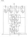
- FIG. 1 is a view illustrating a prior art general sustain driver and gate driver
- FIG. 2 is a view illustrating an embodiment of a plasma display apparatus in accordance with the invention.
- FIG. 3 is a view illustrating an embodiment of a structure of a plasma display panel shown in FIG. 2;
- FIG. 4 is a view illustrating an embodiment of a method of driving the plasma display panel in accordance with the invention.
- FIG. 5 is a view illustrating a gate driver and a sustain driver for supplying a sustain signal shown in FIG. 4;
- FIG. 6A is a view illustrating a method of operating a second gate driver shown in FIG. 5;
- FIG. 6B is a view illustrating a method of operating a third gate driver shown in FIG. 5;
- FIG. 7 is a view illustrating the output sustain signal and a switching timing chart of a sustain driver shown in FIG. 5;
- FIGS. 8A to 8H are views illustrating a method of driving the sustain driver depending on switching timing shown in FIG. 7.
- a plasma display apparatus comprises a plasma display panel 200, a first driver 210, a second driver 220, and a third driver 230.
- the first driver 210 and the second driver 220 comprise a sustain driver, and the third driver 230 comprises a data driver.
- the first driver 210 drives first electrodes Y1 to Yn of the plasma display panel 200.
- the first driver 210 comprises the sustain driver and the sustain driver supplies a multi level of sustain signal to the first electrodes Y1 to Yn during a sustain period so that an image is displayed by maintaining a discharge.
- a multi level of sustain signal may comprise voltage levels of a half of a positive sustain voltage and a positive sustain voltage.
- the sustain driver comprises a plurality of switching elements for controlling a sustain signal and the plurality of switching elements is controlled by a gate driver.
- the gate driver comprises at least two types of gate drivers. Examples of embodiments of gate drivers will be described later with reference to FIGS. 5 to 8.
- the first driver 210 is arranged to supply a reset signal in a reset period and a scan reference voltage and a scan signal in an address period to the first electrodes Y1 to Yn so that wall charges are uniformly formed within a discharge cell.
- the second driver 220 drives a second electrode Z of the plasma display panel 200.
- the second driver 220 comprises a sustain driver and the sustain driver supplies a multi level of sustain signal in a sustain period.
- the third driver 230 comprises a data driver, and the data driver supplies a data signal to the third electrodes X1 to Xm formed in the plasma display panel 200 in an address period.
- a front panel 300 and a rear panel 310 are coupled in parallel to each other and spaced apart by a predetermined distance.
- a first electrode 302 (Y) and a second electrode 303 (Z) for maintaining a discharge are formed in a front substrate 301, which is a display surface for displaying an image.
- a plurality of third electrodes 313 (X) is arranged so that the first electrode 302 (Y) and the second electrode 303 (Z) intersect on the rear substrate 311 forming a rear surface.
- the front panel 300 comprises the first electrode 302 (Y) and the second electrode 303 (Z) for performing a mutual discharge and maintaining emission of a discharge cell in a single discharge space, i.e., a discharge cell.
- a sustain electrode the first electrode 302 (Y) and the second electrode 303 (Z) comprising a transparent electrode (a) that is made of a transparent ITO material and a bus electrode (b) that is made of a metal material are formed in pairs.
- the first electrode 302 (Y) and the second electrode 303 (Z) are covered with at least one upper dielectric layer 304 that limits a discharge current and provides isolation between electrode pairs.
- a protective layer 305 deposited with magnesium oxide (MgO) is formed so as to facilitate a discharge condition.
- stripe type (or well type) barrier ribs 312 for forming a plurality of discharge spaces, i.e., discharge cells are arranged in parallel. Furthermore, a plurality of third electrodes 313 (X) for generating vacuum ultraviolet radiation by performing an address discharge are disposed in parallel with the barrier rib 312. R, G, and B phosphors 314 that emit visible light for displaying an image upon an address discharge are coated in the upper side surface of the rear panel 310. A lower dielectric layer 315 for protecting the third electrode 313 (X) is formed between the third electrode 313 (X) and the phosphor 314.
- FIG. 3 shows only an example of a plasma display panel 200, and the invention in its broadest aspect is not limited to panels of such a structure.
- FIG. 3 shows that the first electrode 302 (Y) and the second electrode 303 (Z), which are a sustain electrode, comprise transparent electrodes 302a and 303a and bus electrodes 302b and 303b, respectively, but at least one of the first electrode 302 (Y) and the second electrode 303 (Z) may comprise only the bus electrodes 302b and 303b.
- FIG. 3 shows that the upper dielectric layer 304 has a uniform thickness
- the upper dielectric layer 304 may have a different thickness and dielectric constant for each area
- FIG. 3 shows only a barrier rib 312 having a fixed pitch, in order to match white balance, the spacing of the barrier rib 312 in a discharge cell B can be formed.
- the brightness of an image embodied in the plasma display panel 200 may be increased.
- a tunnel may be formed in a side surface of the barrier rib 312 in order to improve the exhaust characteristics.
- each of drivers 210, 220, and 230 shown in FIG. 2 drives a plurality of electrodes of the plasma display panel 200
- FIG. 4 An embodiment of a driving method in which each of drivers 210, 220, and 230 shown in FIG. 2 drives a plurality of electrodes of the plasma display panel 200 will be described in detail with reference to FIG. 4.
- each of the drivers 210, 220, and 230 shown in FIG. 2 supplies a driving signal to the first electrode Y, the second electrode Z, and the third electrode X during a reset period, an address period, and a sustain period.
- the first driver 210 supplies the same set-up signal as that shown in the first electrode Y in a set-up period of a reset period.
- a weak dark discharge is generated within a discharge cell of an entire screen by the set-up signal. Positive wall charges accumulate on the second electrode Z and the third electrode X by the set-up discharge and negative wall charges accumulate on the first electrode Y.
- the first driver 210 supplies a set-down signal falling from a positive voltage lower than a highest voltage of a set-up signal to a specific voltage level lower than a ground GND level of voltage. Accordingly, a weak erase discharge is generated within the discharge cell, whereby wall charges excessively formed within the discharge cell become fully erased. Wall charges sufficient to stably generate an address discharge by the set-down discharge uniformly remain within the discharge cell.
- FIG. 4 illustrates a case where both a set-up signal and a set-down signal are supplied in a reset period.
- at least one of the set-up signal and the set-down signal may allow a ground level voltage to be maintained and the set-up signal may be a signal which maintains the same level of voltage as the positive sustain voltage during the set-up period.
- the first driver 210 supplies a scan reference voltage Vsc to the first electrode in an address period, and the first driver 210 supplies a scan signal Scan falling from a scan reference voltage Vsc to a negative voltage (-Vy) to the first electrode Y at a time point when a data signal Va supplied by the third driver 230 is supplied to the third electrode during an address period.
- Wall charges sufficient to generate a discharge when a sustain voltage Vs is applied are generated within a discharge cell selected by an address discharge. Accordingly, the first electrode Y is scanned.
- the first driver 210 is shown supplying a scan reference voltage Vsc to the first electrode Y during an address period.
- a scan bias voltage (-Vy+Vsc) may be supplied instead of the scan reference voltage Vsc.
- a sustain driver comprised in the first driver 110 and a sustain driver comprised in the second driver 120 may altemately supply a sustain signal to the first electrode Y and the second electrode Z in a sustain period.
- the sustain signal comprises various voltages such as a half of a positive sustain voltage Vs/2 and a positive sustain voltage Vs.
- a part or all of a sustain signal that is alternately supplied to the first electrode Y and the second electrode Z can be supplied such as to overlap.
- a sustain discharge i.e., a display discharge is generated between the first electrode Y and the second electrode Z.
- An erase period may be further added in a driving method described according to an embodiment.
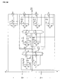
- a sustain driver 500 for supplying a sustain signal comprises first switching elements M20, M30, M40, and M60, second switching elements M50 and M70, third switching elements M10 and M80, a plurality of inductors L1 to L4, and a plurality of capacitors C 11 to C 14 .
- the sustain driver 500 supplies a multi voltage level of sustain signal comprising a half of a positive sustain voltage Vs/2 and a positive sustain voltage Vs.
- the sustain driver 500 comprises at least one of the first driver and the second driver shown in FIG. 1.
- a method of operating the sustain driver 500 will now be described in detail with reference to FIGS. 7 and 8A to 8H.
- First, second, third switching elements M10 to M80 are turned on if a voltage of a gate terminal is higher by 5 to 15V than that of a source terminal and are turned off if a voltage of the gate terminal is lower by 5 to 15V than that of the source terminal.
- Gate drivers for controlling the first, second, third switching elements M10 to M80 by supplying a control signal comprise first gate drivers 510a, 510b, 510c, and 510d, second gate drivers 520a and 520b, and third gate drivers 530a and 530b.
- the first gate drivers 510a, 510b, 510c, and 510d control the first switching elements M20, M30, M40, and M60, respectively depending on each control signal that receives through each of lines HI and LI.
- the first gate drivers 510a, 510b, 510c, and 510d comprise charge capacitors C2, C3, C4, and C6 for forming a driving voltage by storing a voltage that is received from driving voltage sources P2, P3, P4, and P6 and further comprise diodes D2, D3, and D5 so as to secure stability of circuit operation.
- a method of controlling the first switching elements M20, M30, M40, and M60 with the first gate drivers 510a, 510b, 510c, and 510d will now be described using the first gate driver 510c as example.
- a driving voltage source P3 of the gate driver 510c supplies a constant voltage of 15V to the charge capacitor C3 through the diode D3, and a 15V driving voltage stored in the charge capacitor C3 controls the switching element M30 so that a upper switch or a lower switch of the line HI or LI is turned on depending on a control signal received through the line HI or LI.
- the 15V driving voltage stored in the charge capacitor C3 is supplied to the gate terminal G of the switch M30.
- the voltage difference between the gate terminal G and the source terminal S of the switch M30 becomes 15V, whereby the switch M30 is turned on.
- each of the first gate drivers exercises control so that each of the first switching elements is turned on or turned off.
- the second gate drivers 520a and 520b controls the second switching elements M50 and M70, respectively.
- the second gate drivers 520a and 520b comprise charge capacitors C7 and C5 that form a driving voltage by storing the voltage received from driving voltage sources P7 and P5, auxiliary charge capacitors C9 and C10 that receive and store an auxiliary voltage for assisting a driving voltage from the outside of the second gate drivers 520a and 520b so that the second switching elements M50 and M70 drive by a driving voltage, and resistances R1, R2, R3, and R4 that are connected in series to each of both ends of the auxiliary charge capacitors C9 and C10.
- the gate driver 520a will now be described as an example.
- the resistance R2 whose one end is connected between one end of the auxiliary charge capacitor C9 and a gate terminal G of the second switching element M70 and whose the other end is connected in series to one end of the capacitor C12 of the sustain driver 500 performs a function of forming a 15V driving voltage in the gate terminal G and the source terminal S of the second switching element M70 so that the second switching element M70 is turned on.
- the resistance R1 whose one end is connected to the other end of the auxiliary charge capacitor C9 and whose other end is connected to the other end of the capacitor C 12 of the sustain driver 500 performs the function of ensuring stability of the circuit.
- a voltage difference can be formed between the gate terminal and the source terminal of the switching elements M5 and M7 by supplying an auxiliary voltage and thus the switching elements M5 and M7 can be stably controlled.
- the third gate drivers 530a and 530b control the third switching elements M10 and M80, respectively.
- Respective cathodes of diodes D7 and D1 are electrically connected to the charge capacitors C8 and C1 of the third gate drivers 530a and 530b and respective anodes of diodes D7 and D 1 are electrically connected to charge capacitors C6 and C2 of the first gate drivers 510a and 510b.
- the third gate drivers do not comprise a separate driving voltage source, the circuit becomes simplified and the manufacturing cost can be reduced.
- FIG. 5 shows that all of the first, second, and third gate drivers are comprised in a circuit. In a modification, only the first and second gate drivers need be used or only the first and third gate drivers need be used.
- the area and a bulk of the driver circuit can be reduced and as an expensive element for physically embodying the floating voltage source is not used, manufacturing cost can be reduced.
- not all circuits of the gate driver need to comprise only the first gate driver so as to control a switching element of a sustain driver for supplying a multi level of sustain signal.
- driving voltage sources of the gate driver should be connected to the ground and a period when source terminals of all switching elements of the sustain driver has a ground level of voltage GND during driving is required. This is because switching elements that do not satisfy the above condition as in M10, M50, M70, and M80 are always comprised in a sustain driver for supplying a multi level of sustain signal.
- a sustain driver for supplying a multi level of sustain signal always requires a floating voltage source.
- circuit construction can become simpler than that of a gate driver using a floating voltage source.
- FIG. 6A A method of operating a second gate driver shown in FIG. 5 will now be described with reference to FIG. 6A.
- each of the respective second gate drivers 520a and 520b shown in FIG. 5 is connected to respective capacitors C12 and C14 of the sustain driver 500, an auxiliary voltage is supplied from the capacitors C12 and C14 of an external sustain driver 500 and the second gate drivers 520a and 520b.
- an auxiliary voltage is formed by receiving a voltage from the capacitors C12 and C14 of the sustain driver 500 and storing the voltage in auxiliary charge capacitors C9 and C10 that are connected in series with the respective gate terminals G of the second switching elements M50 and M70.
- An exemplary driving method of the second gate drivers 520a and 520b is as follows.
- a gate driver 520a for controlling the switch M70 comprises a 15V driving voltage source, a charge capacitor C7, the auxiliary charge capacitor C9, and resistances R1 and R2.
- the 15V driving voltage is stored in the charge capacitor C7 through the diode D6 from the 15V driving voltage source P7 by a current path (not shown) that is connected to P7(+), D6, C7, and P7(-).
- an auxiliary voltage is transferred from C12 to C9 through a first current path that is connected to C12(+), R2, C9, R1, and C12(-).
- V1 the voltage between both plates that is stored in C 12
- V1 the voltage between both plates that is stored in C 12
- the voltage of the node between R1 and C9 becomes 15V and C9 simply maintains the voltage V1, so that the voltage of the node between C9 and R2 becomes V1+15V.
- the voltage of the C12(-) terminal is connected to ground, the voltage of the C12(+) terminal becomes V1. Accordingly, the voltage of the node between R2 and C12(+) becomes V1.
- a gate driver 520b for controlling the switch M50 comprises the 15V driving voltage source P5, the charge capacitor C5, the auxiliary charge capacitor C10, and resistances R3 and R4 will be described.
- an auxiliary voltage becomes stored from C14 (-) to C10 through a second current path that is connected to C14(+), R4, C10, R3, and C 14.
- the method of turning on the switch M50 by the gate driver 520b is the same as the method of turning on the switch M70 by the gate driver 520a.
- FIG. 6B A method of operating a third gate driver shown in FIG. 5 will now be described with reference to FIG. 6B.
- the third gate drivers 530a and 530b receive a driving voltage for driving the third switching elements M10 and M80 from other gate drivers.
- the third gate drivers 530a and 530b receive a driving voltage of the third gate drivers 530a and 530b from the first gate drivers 510a and 510b.
- the driving method of the third gate drivers 530a and 530b is as follows.
- the gate driver 530a for controlling the switch M80 comprises a charge capacitor C8 and a diode D7.
- the cathode of diode D7 is electrically connected to the charge capacitor C8 of the gate driver 530a and the anode of diode D7 is electrically connected to the charge capacitor C6 of the gate driver 510a.
- the switch M60 for controlling the gate driver 510a is turned on, the 15V driving voltage stored in C6 charges to C8 by the first current path that is connected to C6(+), D7, C8, L2, D9, M60, and C6(-).
- a driving voltage is formed by transferring a voltage from the charge capacitor C2 to the charge capacitor C 1 along the shown second current path and the switch M10 is turned on depending on a control signal supplied to the line HI of the gate driver 530b.
- the sustain driver 500 shown in FIG. 5 supplies a sustain signal comprising a half of a positive sustain voltage and a positive sustain voltage.
- the sustain driver 500 when a sustain signal rises from a ground level to a positive sustain voltage, the sustain signal does not rise at once but in two steps. Accordingly, the withstand voltage rating characteristics of a switching element comprised in the sustain driver 500 can be reduced and thus the manufacturing cost can be reduced.
- sustain driver 500 In an exemplary driving method of the sustain driver 500 is as follows.
- a voltage Vs/2 is stored in each of capacitors C 11 and C 12 of the shown sustain driver 500 and a voltage Vs/4 is stored in the capacitors C13 and C14.
- a voltage Vs means the same voltage as a positive sustain voltage of a sustain signal.
- a current path that is connected to GND, M40, C14, C13, M20, and Vout is formed as in FIG. 8C and thus a sustain signal maintains a half of a positive sustain voltage Vs/2 during a predetermined time.
- the predetermined time can be adjusted depending on the state of wall charges of an inner discharge cell in the plasma display panel and is adjusted depending on the time when the switches M20 and M40 are turned on.
- a switching element having low withstand voltage characteristics can be used in a sustain driver, whereby a manufacturing cost can be reduced.
Landscapes
- Engineering & Computer Science (AREA)
- Physics & Mathematics (AREA)
- Power Engineering (AREA)
- Plasma & Fusion (AREA)
- Computer Hardware Design (AREA)
- General Physics & Mathematics (AREA)
- Theoretical Computer Science (AREA)
- Control Of Indicators Other Than Cathode Ray Tubes (AREA)
- Control Of Gas Discharge Display Tubes (AREA)
- Transforming Electric Information Into Light Information (AREA)
Applications Claiming Priority (1)
| Application Number | Priority Date | Filing Date | Title |
|---|---|---|---|
| KR1020050083862A KR100724366B1 (ko) | 2005-09-08 | 2005-09-08 | 플라즈마 디스플레이 패널을 위한 구동 회로 |
Publications (2)
| Publication Number | Publication Date |
|---|---|
| EP1763010A2 true EP1763010A2 (fr) | 2007-03-14 |
| EP1763010A3 EP1763010A3 (fr) | 2008-05-21 |
Family
ID=37440578
Family Applications (1)
| Application Number | Title | Priority Date | Filing Date |
|---|---|---|---|
| EP06254702A Withdrawn EP1763010A3 (fr) | 2005-09-08 | 2006-09-08 | Appareil d'affichage à plasma |
Country Status (5)
| Country | Link |
|---|---|
| US (1) | US20070052629A1 (fr) |
| EP (1) | EP1763010A3 (fr) |
| JP (1) | JP2007072471A (fr) |
| KR (1) | KR100724366B1 (fr) |
| CN (1) | CN1928956A (fr) |
Families Citing this family (5)
| Publication number | Priority date | Publication date | Assignee | Title |
|---|---|---|---|---|
| KR100796686B1 (ko) | 2006-03-29 | 2008-01-21 | 삼성에스디아이 주식회사 | 플라즈마 표시 장치 및 그 구동 장치와 구동 방법 |
| KR100943956B1 (ko) * | 2008-07-15 | 2010-02-26 | 삼성에스디아이 주식회사 | 플라즈마 표시 장치 및 그 구동 장치 |
| KR101125644B1 (ko) * | 2010-08-09 | 2012-03-28 | 삼성에스디아이 주식회사 | 플라즈마 표시 장치 및 그 구동 장치 |
| US9673713B2 (en) * | 2012-12-04 | 2017-06-06 | Otis Elevator Company | Gate drive power supply for multilevel converter |
| CN113630114A (zh) * | 2021-08-18 | 2021-11-09 | 上海数明半导体有限公司 | 驱动电路以及电子设备 |
Citations (4)
| Publication number | Priority date | Publication date | Assignee | Title |
|---|---|---|---|---|
| US6256215B1 (en) * | 2000-08-10 | 2001-07-03 | Delphi Technologies, Inc. | Multiple output bootstrapped gate drive circuit |
| US20030085886A1 (en) * | 2001-11-06 | 2003-05-08 | Pioneer Corporation | Display panel driving apparatus having a structure capable of reducing power loss |
| EP1450340A2 (fr) * | 2003-02-18 | 2004-08-25 | Fujitsu Hitachi Plasma Display Limited | CIrcuit de pre-commande, circuit de commande de charge capacitive et dispositif d'affichage à plasma |
| EP1657705A2 (fr) * | 2004-11-08 | 2006-05-17 | LG Electronics, Inc. | Appareil d'affichage à plasma et son procédé de commande |
Family Cites Families (5)
| Publication number | Priority date | Publication date | Assignee | Title |
|---|---|---|---|---|
| JPH11338418A (ja) | 1998-05-26 | 1999-12-10 | Mitsubishi Electric Corp | プラズマディスプレイパネルの駆動方法及びプラズマディスプレイ装置 |
| KR100421014B1 (ko) * | 2001-08-28 | 2004-03-04 | 삼성전자주식회사 | 플라즈마 디스플레이 패널 구동 시스템의 자기 결합인덕터를 이용한 전력 회수 장치 및 설계 방법 |
| JP2003280574A (ja) * | 2002-03-26 | 2003-10-02 | Fujitsu Hitachi Plasma Display Ltd | 容量性負荷駆動回路及びプラズマディスプレイ装置 |
| KR100484175B1 (ko) * | 2002-11-08 | 2005-04-18 | 삼성전자주식회사 | 고효율 플라즈마 디스플레이 패널 구동 장치 및 방법 |
| KR100509503B1 (ko) * | 2003-07-10 | 2005-08-22 | 삼성전자주식회사 | 서지 전압을 클램핑하는 플라즈마 디스플레이 패널서스테인 구동 장치 및 방법 |
-
2005
- 2005-09-08 KR KR1020050083862A patent/KR100724366B1/ko not_active IP Right Cessation
-
2006
- 2006-09-07 US US11/516,749 patent/US20070052629A1/en not_active Abandoned
- 2006-09-08 CN CNA2006101537118A patent/CN1928956A/zh active Pending
- 2006-09-08 EP EP06254702A patent/EP1763010A3/fr not_active Withdrawn
- 2006-09-08 JP JP2006244091A patent/JP2007072471A/ja not_active Withdrawn
Patent Citations (4)
| Publication number | Priority date | Publication date | Assignee | Title |
|---|---|---|---|---|
| US6256215B1 (en) * | 2000-08-10 | 2001-07-03 | Delphi Technologies, Inc. | Multiple output bootstrapped gate drive circuit |
| US20030085886A1 (en) * | 2001-11-06 | 2003-05-08 | Pioneer Corporation | Display panel driving apparatus having a structure capable of reducing power loss |
| EP1450340A2 (fr) * | 2003-02-18 | 2004-08-25 | Fujitsu Hitachi Plasma Display Limited | CIrcuit de pre-commande, circuit de commande de charge capacitive et dispositif d'affichage à plasma |
| EP1657705A2 (fr) * | 2004-11-08 | 2006-05-17 | LG Electronics, Inc. | Appareil d'affichage à plasma et son procédé de commande |
Also Published As
| Publication number | Publication date |
|---|---|
| EP1763010A3 (fr) | 2008-05-21 |
| KR20070029004A (ko) | 2007-03-13 |
| US20070052629A1 (en) | 2007-03-08 |
| KR100724366B1 (ko) | 2007-06-04 |
| JP2007072471A (ja) | 2007-03-22 |
| CN1928956A (zh) | 2007-03-14 |
Similar Documents
| Publication | Publication Date | Title |
|---|---|---|
| US6469452B2 (en) | Plasma display panel and its driving method | |
| US20060103325A1 (en) | Plasma display device and driving method with reduced displacement current | |
| EP1796068B1 (fr) | Appareil d'affichage à plasma | |
| EP1763010A2 (fr) | Appareil d'affichage à plasma | |
| US20070052626A1 (en) | Plasma display apparatus | |
| US7692608B2 (en) | Energy recovery circuit and energy recovering method using the same | |
| US8325110B2 (en) | Power supply and driver for plasma display panel | |
| EP1811490A1 (fr) | Appareil d'affichage à plasma et son procédé de commande | |
| US20060203431A1 (en) | Plasma display panel (PDP) driving apparatus | |
| US7768478B2 (en) | Plasma display apparatus | |
| US7928931B2 (en) | Plasma display apparatus | |
| US7868853B2 (en) | Driving device for plasma display panel and plasma display device including the driving device | |
| KR100800521B1 (ko) | 플라즈마 디스플레이 장치 및 그의 구동 방법 | |
| KR100488462B1 (ko) | 에너지 회수장치 및 방법 | |
| KR100381267B1 (ko) | 플라즈마 디스플레이 패널의 구동장치 및 그의 구동방법 | |
| KR100877820B1 (ko) | 플라즈마 디스플레이 장치 | |
| US20080007489A1 (en) | Apparatus for driving plasma display panel | |
| US7999764B2 (en) | Plasma display apparatus | |
| US7924241B2 (en) | Plasma display apparatus and method of driving the same | |
| KR100811524B1 (ko) | 플라즈마 디스플레이 장치 | |
| US7928930B2 (en) | Plasma display apparatus | |
| KR100754881B1 (ko) | 플라즈마 디스플레이 패널의 유지 구동 장치 및 그구동방법 | |
| KR100553936B1 (ko) | 에너지 회수장치 및 방법 | |
| KR20070106332A (ko) | 플라즈마 디스플레이 장치 |
Legal Events
| Date | Code | Title | Description |
|---|---|---|---|
| PUAI | Public reference made under article 153(3) epc to a published international application that has entered the european phase |
Free format text: ORIGINAL CODE: 0009012 |
|
| AK | Designated contracting states |
Kind code of ref document: A2 Designated state(s): AT BE BG CH CY CZ DE DK EE ES FI FR GB GR HU IE IS IT LI LT LU LV MC NL PL PT RO SE SI SK TR |
|
| AX | Request for extension of the european patent |
Extension state: AL BA HR MK YU |
|
| PUAL | Search report despatched |
Free format text: ORIGINAL CODE: 0009013 |
|
| AK | Designated contracting states |
Kind code of ref document: A3 Designated state(s): AT BE BG CH CY CZ DE DK EE ES FI FR GB GR HU IE IS IT LI LT LU LV MC NL PL PT RO SE SI SK TR |
|
| AX | Request for extension of the european patent |
Extension state: AL BA HR MK RS |
|
| AKX | Designation fees paid | ||
| REG | Reference to a national code |
Ref country code: DE Ref legal event code: 8566 |
|
| STAA | Information on the status of an ep patent application or granted ep patent |
Free format text: STATUS: THE APPLICATION IS DEEMED TO BE WITHDRAWN |
|
| 18D | Application deemed to be withdrawn |
Effective date: 20081122 |