EP1763007A2 - Method for driving display panel - Google Patents
Method for driving display panel Download PDFInfo
- Publication number
- EP1763007A2 EP1763007A2 EP06018461A EP06018461A EP1763007A2 EP 1763007 A2 EP1763007 A2 EP 1763007A2 EP 06018461 A EP06018461 A EP 06018461A EP 06018461 A EP06018461 A EP 06018461A EP 1763007 A2 EP1763007 A2 EP 1763007A2
- Authority
- EP
- European Patent Office
- Prior art keywords
- display
- half section
- period
- emission
- display line
- Prior art date
- Legal status (The legal status is an assumption and is not a legal conclusion. Google has not performed a legal analysis and makes no representation as to the accuracy of the status listed.)
- Withdrawn
Links
- 238000000034 method Methods 0.000 title claims abstract description 26
- 238000007599 discharging Methods 0.000 description 65
- 238000010586 diagram Methods 0.000 description 9
- 238000006243 chemical reaction Methods 0.000 description 7
- 241001270131 Agaricus moelleri Species 0.000 description 4
- 238000009792 diffusion process Methods 0.000 description 3
- 239000011159 matrix material Substances 0.000 description 3
- 230000002093 peripheral effect Effects 0.000 description 2
- 230000004044 response Effects 0.000 description 1
Images


Classifications
-
- G—PHYSICS
- G09—EDUCATION; CRYPTOGRAPHY; DISPLAY; ADVERTISING; SEALS
- G09G—ARRANGEMENTS OR CIRCUITS FOR CONTROL OF INDICATING DEVICES USING STATIC MEANS TO PRESENT VARIABLE INFORMATION
- G09G3/00—Control arrangements or circuits, of interest only in connection with visual indicators other than cathode-ray tubes
- G09G3/20—Control arrangements or circuits, of interest only in connection with visual indicators other than cathode-ray tubes for presentation of an assembly of a number of characters, e.g. a page, by composing the assembly by combination of individual elements arranged in a matrix no fixed position being assigned to or needed to be assigned to the individual characters or partial characters
- G09G3/22—Control arrangements or circuits, of interest only in connection with visual indicators other than cathode-ray tubes for presentation of an assembly of a number of characters, e.g. a page, by composing the assembly by combination of individual elements arranged in a matrix no fixed position being assigned to or needed to be assigned to the individual characters or partial characters using controlled light sources
- G09G3/28—Control arrangements or circuits, of interest only in connection with visual indicators other than cathode-ray tubes for presentation of an assembly of a number of characters, e.g. a page, by composing the assembly by combination of individual elements arranged in a matrix no fixed position being assigned to or needed to be assigned to the individual characters or partial characters using controlled light sources using luminous gas-discharge panels, e.g. plasma panels
- G09G3/288—Control arrangements or circuits, of interest only in connection with visual indicators other than cathode-ray tubes for presentation of an assembly of a number of characters, e.g. a page, by composing the assembly by combination of individual elements arranged in a matrix no fixed position being assigned to or needed to be assigned to the individual characters or partial characters using controlled light sources using luminous gas-discharge panels, e.g. plasma panels using AC panels
- G09G3/291—Control arrangements or circuits, of interest only in connection with visual indicators other than cathode-ray tubes for presentation of an assembly of a number of characters, e.g. a page, by composing the assembly by combination of individual elements arranged in a matrix no fixed position being assigned to or needed to be assigned to the individual characters or partial characters using controlled light sources using luminous gas-discharge panels, e.g. plasma panels using AC panels controlling the gas discharge to control a cell condition, e.g. by means of specific pulse shapes
-
- G—PHYSICS
- G09—EDUCATION; CRYPTOGRAPHY; DISPLAY; ADVERTISING; SEALS
- G09G—ARRANGEMENTS OR CIRCUITS FOR CONTROL OF INDICATING DEVICES USING STATIC MEANS TO PRESENT VARIABLE INFORMATION
- G09G3/00—Control arrangements or circuits, of interest only in connection with visual indicators other than cathode-ray tubes
- G09G3/20—Control arrangements or circuits, of interest only in connection with visual indicators other than cathode-ray tubes for presentation of an assembly of a number of characters, e.g. a page, by composing the assembly by combination of individual elements arranged in a matrix no fixed position being assigned to or needed to be assigned to the individual characters or partial characters
- G09G3/22—Control arrangements or circuits, of interest only in connection with visual indicators other than cathode-ray tubes for presentation of an assembly of a number of characters, e.g. a page, by composing the assembly by combination of individual elements arranged in a matrix no fixed position being assigned to or needed to be assigned to the individual characters or partial characters using controlled light sources
- G09G3/28—Control arrangements or circuits, of interest only in connection with visual indicators other than cathode-ray tubes for presentation of an assembly of a number of characters, e.g. a page, by composing the assembly by combination of individual elements arranged in a matrix no fixed position being assigned to or needed to be assigned to the individual characters or partial characters using controlled light sources using luminous gas-discharge panels, e.g. plasma panels
- G09G3/288—Control arrangements or circuits, of interest only in connection with visual indicators other than cathode-ray tubes for presentation of an assembly of a number of characters, e.g. a page, by composing the assembly by combination of individual elements arranged in a matrix no fixed position being assigned to or needed to be assigned to the individual characters or partial characters using controlled light sources using luminous gas-discharge panels, e.g. plasma panels using AC panels
- G09G3/291—Control arrangements or circuits, of interest only in connection with visual indicators other than cathode-ray tubes for presentation of an assembly of a number of characters, e.g. a page, by composing the assembly by combination of individual elements arranged in a matrix no fixed position being assigned to or needed to be assigned to the individual characters or partial characters using controlled light sources using luminous gas-discharge panels, e.g. plasma panels using AC panels controlling the gas discharge to control a cell condition, e.g. by means of specific pulse shapes
- G09G3/293—Control arrangements or circuits, of interest only in connection with visual indicators other than cathode-ray tubes for presentation of an assembly of a number of characters, e.g. a page, by composing the assembly by combination of individual elements arranged in a matrix no fixed position being assigned to or needed to be assigned to the individual characters or partial characters using controlled light sources using luminous gas-discharge panels, e.g. plasma panels using AC panels controlling the gas discharge to control a cell condition, e.g. by means of specific pulse shapes for address discharge
- G09G3/2935—Addressed by erasing selected cells that are in an ON state
-
- G—PHYSICS
- G09—EDUCATION; CRYPTOGRAPHY; DISPLAY; ADVERTISING; SEALS
- G09G—ARRANGEMENTS OR CIRCUITS FOR CONTROL OF INDICATING DEVICES USING STATIC MEANS TO PRESENT VARIABLE INFORMATION
- G09G3/00—Control arrangements or circuits, of interest only in connection with visual indicators other than cathode-ray tubes
- G09G3/20—Control arrangements or circuits, of interest only in connection with visual indicators other than cathode-ray tubes for presentation of an assembly of a number of characters, e.g. a page, by composing the assembly by combination of individual elements arranged in a matrix no fixed position being assigned to or needed to be assigned to the individual characters or partial characters
- G09G3/2007—Display of intermediate tones
- G09G3/2018—Display of intermediate tones by time modulation using two or more time intervals
- G09G3/2022—Display of intermediate tones by time modulation using two or more time intervals using sub-frames
- G09G3/2029—Display of intermediate tones by time modulation using two or more time intervals using sub-frames the sub-frames having non-binary weights
-
- G—PHYSICS
- G09—EDUCATION; CRYPTOGRAPHY; DISPLAY; ADVERTISING; SEALS
- G09G—ARRANGEMENTS OR CIRCUITS FOR CONTROL OF INDICATING DEVICES USING STATIC MEANS TO PRESENT VARIABLE INFORMATION
- G09G3/00—Control arrangements or circuits, of interest only in connection with visual indicators other than cathode-ray tubes
- G09G3/20—Control arrangements or circuits, of interest only in connection with visual indicators other than cathode-ray tubes for presentation of an assembly of a number of characters, e.g. a page, by composing the assembly by combination of individual elements arranged in a matrix no fixed position being assigned to or needed to be assigned to the individual characters or partial characters
- G09G3/2007—Display of intermediate tones
- G09G3/2018—Display of intermediate tones by time modulation using two or more time intervals
- G09G3/2022—Display of intermediate tones by time modulation using two or more time intervals using sub-frames
- G09G3/204—Display of intermediate tones by time modulation using two or more time intervals using sub-frames the sub-frames being organized in consecutive sub-frame groups
-
- G—PHYSICS
- G09—EDUCATION; CRYPTOGRAPHY; DISPLAY; ADVERTISING; SEALS
- G09G—ARRANGEMENTS OR CIRCUITS FOR CONTROL OF INDICATING DEVICES USING STATIC MEANS TO PRESENT VARIABLE INFORMATION
- G09G3/00—Control arrangements or circuits, of interest only in connection with visual indicators other than cathode-ray tubes
- G09G3/20—Control arrangements or circuits, of interest only in connection with visual indicators other than cathode-ray tubes for presentation of an assembly of a number of characters, e.g. a page, by composing the assembly by combination of individual elements arranged in a matrix no fixed position being assigned to or needed to be assigned to the individual characters or partial characters
- G09G3/22—Control arrangements or circuits, of interest only in connection with visual indicators other than cathode-ray tubes for presentation of an assembly of a number of characters, e.g. a page, by composing the assembly by combination of individual elements arranged in a matrix no fixed position being assigned to or needed to be assigned to the individual characters or partial characters using controlled light sources
- G09G3/28—Control arrangements or circuits, of interest only in connection with visual indicators other than cathode-ray tubes for presentation of an assembly of a number of characters, e.g. a page, by composing the assembly by combination of individual elements arranged in a matrix no fixed position being assigned to or needed to be assigned to the individual characters or partial characters using controlled light sources using luminous gas-discharge panels, e.g. plasma panels
- G09G3/288—Control arrangements or circuits, of interest only in connection with visual indicators other than cathode-ray tubes for presentation of an assembly of a number of characters, e.g. a page, by composing the assembly by combination of individual elements arranged in a matrix no fixed position being assigned to or needed to be assigned to the individual characters or partial characters using controlled light sources using luminous gas-discharge panels, e.g. plasma panels using AC panels
- G09G3/296—Driving circuits for producing the waveforms applied to the driving electrodes
-
- G—PHYSICS
- G09—EDUCATION; CRYPTOGRAPHY; DISPLAY; ADVERTISING; SEALS
- G09G—ARRANGEMENTS OR CIRCUITS FOR CONTROL OF INDICATING DEVICES USING STATIC MEANS TO PRESENT VARIABLE INFORMATION
- G09G2310/00—Command of the display device
- G09G2310/06—Details of flat display driving waveforms
-
- G—PHYSICS
- G09—EDUCATION; CRYPTOGRAPHY; DISPLAY; ADVERTISING; SEALS
- G09G—ARRANGEMENTS OR CIRCUITS FOR CONTROL OF INDICATING DEVICES USING STATIC MEANS TO PRESENT VARIABLE INFORMATION
- G09G2320/00—Control of display operating conditions
- G09G2320/02—Improving the quality of display appearance
- G09G2320/0247—Flicker reduction other than flicker reduction circuits used for single beam cathode-ray tubes
-
- G—PHYSICS
- G09—EDUCATION; CRYPTOGRAPHY; DISPLAY; ADVERTISING; SEALS
- G09G—ARRANGEMENTS OR CIRCUITS FOR CONTROL OF INDICATING DEVICES USING STATIC MEANS TO PRESENT VARIABLE INFORMATION
- G09G3/00—Control arrangements or circuits, of interest only in connection with visual indicators other than cathode-ray tubes
- G09G3/20—Control arrangements or circuits, of interest only in connection with visual indicators other than cathode-ray tubes for presentation of an assembly of a number of characters, e.g. a page, by composing the assembly by combination of individual elements arranged in a matrix no fixed position being assigned to or needed to be assigned to the individual characters or partial characters
- G09G3/2007—Display of intermediate tones
- G09G3/2044—Display of intermediate tones using dithering
- G09G3/2051—Display of intermediate tones using dithering with use of a spatial dither pattern
-
- G—PHYSICS
- G09—EDUCATION; CRYPTOGRAPHY; DISPLAY; ADVERTISING; SEALS
- G09G—ARRANGEMENTS OR CIRCUITS FOR CONTROL OF INDICATING DEVICES USING STATIC MEANS TO PRESENT VARIABLE INFORMATION
- G09G3/00—Control arrangements or circuits, of interest only in connection with visual indicators other than cathode-ray tubes
- G09G3/20—Control arrangements or circuits, of interest only in connection with visual indicators other than cathode-ray tubes for presentation of an assembly of a number of characters, e.g. a page, by composing the assembly by combination of individual elements arranged in a matrix no fixed position being assigned to or needed to be assigned to the individual characters or partial characters
- G09G3/22—Control arrangements or circuits, of interest only in connection with visual indicators other than cathode-ray tubes for presentation of an assembly of a number of characters, e.g. a page, by composing the assembly by combination of individual elements arranged in a matrix no fixed position being assigned to or needed to be assigned to the individual characters or partial characters using controlled light sources
- G09G3/28—Control arrangements or circuits, of interest only in connection with visual indicators other than cathode-ray tubes for presentation of an assembly of a number of characters, e.g. a page, by composing the assembly by combination of individual elements arranged in a matrix no fixed position being assigned to or needed to be assigned to the individual characters or partial characters using controlled light sources using luminous gas-discharge panels, e.g. plasma panels
Definitions
- the present invention relates to a method for driving a matrix display type display panel.
- a plasma display panel (hereafter referred to as PDP) having a plurality of discharge cells arranged in a matrix pattern draws attention as a two-dimensional image display panel.
- PDP plasma display panel
- a subfield method which displays an image corresponding to an input video signal on a PDP has been known.
- a display period of one field is divided into a plurality of subfields, and each of the discharge cells is selectively discharged for emission in each subfield in accordance with a brightness level indicated by the input video signal.
- intermediate brightness corresponding to an overall emission period within one field period is visually recognized.
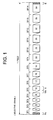
- Fig. 1 shows an example of an emission drive sequence based on the subfield method (see for example Japanese Patent Application Laid-Open No. 2000-227778 , Fig. 14).
- one field period is divided into 14 subfields, i.e., subfields SF1 to SF14. Only in the first subfield SF1 among the subfields SF1 to SF14, all the discharge cells of the PDP are initialized into light ON mode (Rc). Further, in each of the subfields SF1 to SF14, a discharge cell is set to light OFF mode depending on the input video signal (Wc), and only a display cell set to light ON mode is discharged for emission during a period assigned to this subfield (Ic).
- Fig. 2 shows an example of an emission drive pattern within one field period of one discharge cell, which is driven based on such emission drive sequence (see for example Japanese Patent Application Laid-Open No. 2000-227778 , Fig. 27).
- a discharge cell which has been initialized to the light ON mode in the first subfield SF1 is selectively erase-discharged in one of the subfields SF1 to SF14 so as to set to light OFF mode as shown by black dots.
- a discharge cell which is once set to light OFF mode maintains its light OFF mode until the subfield SF14 at the very end.
- a discharge cell is continuously discharged for emission in subfields shown by white circles from the first subfield SF1. Since each of the 15 types of emission patterns shown in Fig. 2 has a different total emission period in one field period, 15 types of intermediate brightness can be represented. In short, (N + 1) grayscales (N is the number of subfields) of intermediate brightness display is possible.
- multi-grayscale processing such as error diffusion and dither processing, is performed for the input video signal.
- the input video signal is converted into, for example, 8-bit pixel data for each pixel where the significant 6 bits thereof are recognized as the display data and the remaining insignificant 2 bits are recognized as error data.
- Error data corresponding to the peripheral pixels are respectively weighted and then added to each other so as to incorporate into the display data concerned.
- the brightness of the insignificant 2 bits in an original pixel is artificially represented by the peripheral pixels, and therefore the grayscale representation of the brightness equivalent to the 8 bits of pixel data becomes possible by 6 bits of display data.
- Dither processing is then performed on the 6 bits of error diffusion-processed pixel data acquired by the above-described error diffusion processing.
- a plurality of adjacent pixels are regarded as one pixel unit, and different dither coefficients are respectively assigned and added to the pixels in this one pixel unit where each of the pixels corresponds to the error diffusion-processed pixel data.
- brightness equivalent to 8 bits can be represented only by the significant 4 bits of the dither-added pixel data in terms of one pixel unit.
- the significant 4 bits of the dither-added pixel data are extracted as the multi-grayscale pixel data Ds, and those data are respectively assigned to the 15 types of emission patterns, as shown in Fig. 2.
- a pseudo-pattern called a dither pattern which is not related to the input video signal, may be visually recognized, which deteriorates image quality.
- the switching from emission sustaining status to light OFF status is once or less within one field period, and therefore the switching frequency is the same as the vertical synchronizing frequency which determines one field display period. Therefore if a PAL type television signal, of which vertical synchronizing frequency is only 50 [Hz], is supplied as the input video signal, flickers tend to be outstanding.
- the present invention is provided to solve the foregoing problems, and an object of the present invention is to provide a method for driving a display panel which allows good image display where flickers and dither patterns are suppressed.
- a method for driving a display panel having a plurality of display lines each provided with a plurality of pixel cells, said pixel cells are driven by a plurality of subfields within each unit display period comprising: a drive step for respectively assigning different brightness weight values to a series of M (M is an integer 2 or higher) display lines belonging to each of display line groups, and for emitting said pixel cells based on said brightness weight values such that an emission period of a pixel cell belonging to one display line differs from that of another pixel cell belonging to another display line among said M display lines, wherein said drive step comprises a first half drive step for executing emission of a first period out of said emission period in a first half section of said unit display period, and a latter half drive step for executing emission of a remaining second period out of said emission period in a latter half section of said unit display period, and relationship of a length of said first period to a length of said second period is reversed between one pixel cell belonging
- a method for driving a display panel having a plurality of display lines each provided with a plurality of pixel cells, said display panel is driven to display grayscale by a plurality of subfields in each unit display period in accordance with an input video signal comprising: emitting one pixel cell belonging to one display line by P subfields (P is an integer) continuously placed in a first half section of said unit display period and by Q subfields (Q is an integer less than P) continuously placed in a latter half section of said unit display period, and emitting another pixel cell belonging to another display line adjacent to said one display line by Q subfields continuously placed in the first half section of said unit display period and by P subfields continuously placed in the latter half section of said unit display period, when the Kth grayscale display is performed, and emitting one pixel cell belonging to said one display line by said P subfields similara to said Kth grayscale display in the first half section of said unit display period, and by said Q subfields similar to
- a method for driving a display panel respectively assigns brightness weight values to a plurality of successive display lines belonging to each of display line groups.
- An emission period within a unit display period of one pixel cell belonging to one display line differs from that of another pixel cell belonging to another display line based on this brightness weight values.
- the emission operation of the pixel cell during this emission period is separated into a first half section and a latter half section within a unit display period. Further, relationship of the length of an emission period in the first half section to that in the latter half section is reversed between one discharge cell belonging to one display line and another discharge cell belonging to another display line among the same display line group.
- frequency to change the status of the discharge cell from light ON status to light OFF status is twice per a unit display period. Accordingly, a good display with suppressed flickers can be performed even if an input video signal with low vertical synchronizing frequency such as PAL type television signal is supplied. Further, emission patterns of a series of 8 display lines change in a unit display period in a manner different from the line dither pattern corresponding to the brightness weight values fixedly assigned to the 8 display lines, and therefore the generation of a line dither pattern can be suppressed.
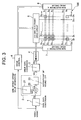
- Fig. 3 is a diagram showing a schematic configuration of a plasma display device for driving a plasma display panel according to the method of the present invention.
- the PDP 100 as a plasma display panel has column electrodes D1 to Dm extending in the vertical direction, and row electrodes X1 to Xn and row electrodes Y1 to Yn extending in the horizontal direction of the two dimensional display screen.
- the row electrodes X1 to Xn and row electrodes Y1 to Yn are alternately arranged one by one.
- the PDP 100 has a first display line including row electrodes X1 and Y1, a second display line including row electrodes X2 and Y2, ... and an n-th display line including row electrodes Xn and Yn.
- a discharge space is provided between these first to n-th display lines and the column electrodes D1 to Dm so as to seal discharge gas therebetween, and a plurality of discharge cells each corresponding to a pixel are respectively formed at intersections between the row electrodes and the column electrodes including the discharge space.
- the PDP 100 thus has (n ⁇ m) discharge cells G (1, 1) to G (n, m) which are arranged in a matrix pattern.
- a pixel data conversion circuit 1 converts an input video signal into pixel data PD of, for example, 8 bits which represents a brightness level of a pixel, and supplies the pixel data PD to a multi-grayscale processing circuit 2. It should be noted that the input video signal mentioned above is obtained after gamma correction on a source video signal corresponding to the image to be displayed.
- the multi-grayscale processing circuit 2 includes a line dither offset value generation circuit 21, adder 22 and insignificant bit round-off circuit 23.
- the line dither offset value generation circuit 21 first generates 8 line dither offset values LD respectively having the values of, for example, 0 through 7 such that these values respectively correspond to the following 8 display line sets, which are formed by dividing a first to n-th display lines of the PDP 100 in a manner that each of the sets is provided with a plurality of display lines of every eighth display line:
- the line dither offset value generation circuit 21 then supplies the line dither offset value LD to the adder 22 such that the line dither offset value LD corresponds to the display line which includes the discharge cell of the pixel data PD supplied from the pixel data conversion circuit 1.
- the adder 22 supplies the line offset added pixel data LF, which is obtained by addition of the line dither offset value LD with the pixel data PD, to an insignificant bit round-off circuit 23.
- the insignificant bit round-off circuit 23 rounds off the insignificant 3 bits of the line offset added pixel data LF, and supplies the remaining significant 3 bits to a drive data conversion circuit 3 as multi-grayscale pixel data MD.
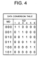
- the drive data conversion circuit 3 converts the 3 bit multi-grayscale pixel data MD to 6 bit pixel drive data GD in accordance with a data conversion table shown in Fig. 4, and supplies it to a memory 4.
- the memory 4 sequentially receives and stores the pixel drive data GD of each pixel. Upon completion of the writing of pixel drive data GD 1 , 1 to GD n, m of one image frame (n rows ⁇ m columns), the memory 4 separates each of the pixel drive data GD 1, 1 to GD n , m into bit digits, and reads one display line at a time. The memory 4 reads pixel drive data bits of the one display line (m bits), and supplies them to a column electrode drive circuit 5 as the pixel drive data bits DB1 to DB(m).
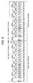
- the drive control circuit 6 generates various timing signals for grayscale driving the PDP 100 in accordance with the emission drive sequence shown in Fig. 5, and supplies them to the column electrode drive circuit 5, row electrode Y drive circuit 7 and row electrode X drive circuit 8 respectively.
- Each of the column electrode drive circuit 5, row electrode Y drive circuit 7 and row electrode X drive circuit 8 generates various drive pulses (not shown) for driving the PDP 100 as described below in response to a timing signal supplied from the drive control circuit 6, and applies them to the column electrodes D1 to Dm, row electrodes X1 to Xn and row electrodes Y1 to Yn of the PDP 100.
- the following six subfields SF0 to SF5 are used so as to represent the various brightness levels for displaying one frame or one field of image in six levels.
- the subfield SF0 determines whether the lowest brightness level 0 is represented or a higher brightness level is represented.
- the subfield SF0 is comprised of a low-level subfield SF0 a placed in the beginning of the first half section of a unit display period, i.e., one frame or one field display period, and a low-level subfield SF0 b placed in the beginning of the latter half section thereof, as shown in Fig. 5.
- the drive control circuit 6 executes a reset step R for initializing all the discharge cells to light ON mode status, where a predetermined amount of wall charges are formed, and an address step W0 for selectively erase-discharging discharge cells depending on the pixel drive data GD from the first to n-th display lines of the PDP 100 in a manner that each display line is erase-discharged at a time.
- the subfield SF1 serves to provide emission with higher brightness level than the lowest brightness level 0 by only one level.
- the subfield SF1 is comprised of 8 low-level subfields SF1 a1 to SF1 a4 and SF1 b1 to SF1 b4 , as shown in Fig. 5, so as to differentiate a brightness level of emission of one discharge cell belonging to one display line from that of another discharge cell belonging to another display line among 8 display lines of each display line group. In this case, as shown in Fig.
- the drive control circuit 6 sequentially executes the sustain step I for repeatedly sustain-discharging the display cells which are set to light ON mode, during a period extending over 2, and the address step W7 for selectively erase-discharging only the discharge cells placed in the (8N-1)th display line in accordance with the pixel drive data GD.
- the drive control circuit 6 sequentially executes the sustain step I for repeatedly sustain-discharging the discharge cells which are set to light ON mode, during a period extending over 2, and the address step W5 for selectively erase-discharging only the discharge cells placed in the (8N-3)th display line in accordance with the pixel drive data GD.
- the drive control circuit 6 sequentially executes the sustain step I for repeatedly sustain-discharging the discharge cells which are set to light ON mode, during a period extending over 2, and the address step W3 for selectively erase-discharging only the discharge cells placed in the (8N-5)th display line in accordance with the pixel drive data GD.
- the drive control circuit 6 sequentially executes the sustain step I for repeatedly sustain-discharging the discharge cells which are set to light ON mode, during a period extending over 2, and the address step W1 for selectively erase-discharging only the discharge cells placed in the (8N-7)th display line in accordance with the pixel drive data GD.
- the drive control circuit 6 sequentially executes the sustain step I for repeatedly sustain-discharging the discharge cells which are set to light ON mode, during a period extending over 1, and the address step W8 for selectively erase-discharging only the discharge cells placed in the (8N)th display line in accordance with the pixel drive data GD.
- the drive control circuit 6 sequentially executes the sustain step I for repeatedly sustain-discharging the discharge cells which are set to light ON mode, during a period extending over 2, and the address step W6 for selectively erase-discharging only the discharge cells placed in the (8N-2)th display line in accordance with the pixel drive data GD.
- the drive control circuit 6 sequentially executes the sustain step I for repeatedly sustain-discharging the discharge cells which are set to light ON mode, during a period extending over 2, and the address step W4 for selectively erase-discharging only the discharge cells placed in the (8N-4)th display line in accordance with the pixel drive data GD.
- the drive control circuit 6 sequentially executes the sustain step I for repeatedly sustain-discharging the discharge cells which are set to light ON mode, during a period extending over 2, and the address step W2 for selectively erase-discharging only the discharge cells placed in the (8N-6)th display line in accordance with the pixel drive data GD.
- the subfield SF2 serves to provide emission with higher brightness level than the subfield SF1 by only one level.
- the subfield SF2 is comprised of 8 low-level subfields SF2 a1 to SF2 a4 and SF2 b1 to SF2 b4 , as shown in Fig. 5, so as to differentiate a brightness level of emission of one discharge cell belonging to one display line from that of another discharge cell belonging to another display line among 8 display lines of each display line group.
- Fig. 5 8 low-level subfields SF2 a1 to SF2 a4 and SF2 b1 to SF2 b4 , as shown in Fig. 5, so as to differentiate a brightness level of emission of one discharge cell belonging to one display line from that of another discharge cell belonging to another display line among 8 display lines of each display line group.
- FIG. 5 shows, 4 low-level subfields SF2 a1 to SF2 a4 , out of these 8 low-level subfields, are placed after the low-level subfield SF1 a4 in the first half section of the unit display period, and the remaining low-level subfields SF2 b1 to SF2 b4 are placed after the low-level subfield SF1 b4 in the latter half section of the unit display period.
- the drive control circuit 6 sequentially executes the sustain step I for repeatedly sustain-discharging the discharge cells which are set to light ON mode, during a period extending over 1, and the address step W8 for selectively erase-discharging only the discharge cells placed in the (8N)th display line in accordance with the pixel drive data GD.
- the drive control circuit 6 sequentially executes the sustain step I for repeatedly sustain-discharging the discharge cells which are set to light ON mode, during a period extending over 2, and the address step W6 for selectively erase-discharging only the discharge cells placed in the (8N-2)th display line in accordance with the pixel drive data GD.
- the drive control circuit 6 sequentially executes the sustain step I for repeatedly sustain-discharging the discharge cells which are set to light ON mode, during a period extending over 2, and the address step W4 for selectively erase-discharging only the discharge cells placed in the (8N-4)th display line in accordance with the pixel drive data GD.
- the drive control circuit 6 sequentially executes the sustain step I for repeatedly sustain-discharging the discharge cells which are set to light ON mode, during a period extending over 2, and the address step W2 for selectively erase-discharging only the discharge cells placed in the (8N-6)th display line in accordance with the pixel drive data GD.
- the drive control circuit 6 sequentially executes the sustain step I for repeatedly sustain-discharging the discharge cells which are set to light ON mode, during a period extending over 3, and the address step W7 for selectively erase-discharging only the discharge cells placed in the (8N-1)th display line in accordance with the pixel drive data GD.
- the drive control circuit 6 sequentially executes the sustain step I for repeatedly sustain-discharging the discharge cells which are set to light ON mode, during a period extending over 2, and the address step W5 for selectively erase-discharging only the discharge cells placed in the (8N-3)th display line in accordance with the pixel drive data GD.
- the drive control circuit 6 sequentially executes the sustain step I for repeatedly sustain-discharging the discharge cells which are set to light ON mode, during a period extending over 2, and the address steps W3 for selectively erase-discharging only the discharge cells placed in the (8N-5)th display line according to the pixel data GD.
- the drive control circuit 6 sequentially executes the sustain step I for repeatedly sustain-discharging the discharge cells which are set to light ON mode, during a period extending over 2, and the address step W1 for selectively erase-discharging only the discharge cells placed in the (8N-7)th display line in accordance with the pixel drive data GD.
- the subfield SF3 serves to provide emission with higher brightness than the subfield SF2 by only one level.
- the subfield SF3 is comprised of 8 low-level subfields SF3 a1 to SF3 a4 and SF3 b1 to SF3 b4 , as shown in Fig. 5, so as to differentiate a brightness level of emission of one discharge cell belonging to one display line from that of another discharge cell belonging to another display line among 8 display lines of each display line group.
- Fig. 5 8 low-level subfields SF3 a1 to SF3 a4 and SF3 b1 to SF3 b4 , as shown in Fig. 5, so as to differentiate a brightness level of emission of one discharge cell belonging to one display line from that of another discharge cell belonging to another display line among 8 display lines of each display line group.
- FIG. 5 shows, 4 low-level subfields SF3 a1 to SF3 a4 , out of these 8 low-level subfields, are placed after the low-level subfield SF2 a4 in the first half section of the unit display period, and the remaining low-level subfields SF3 b1 to SF3 b4 are placed after the low-level subfield SF2 b4 in the latter half section of the unit display period.
- the drive control circuit 6 sequentially executes the sustain step I for repeatedly sustain-discharging the discharge cells which are set to light ON mode, during a period extending over 5, and the address step W7 for selectively erase-discharging only the discharge cells placed in the (8N-1)th display line in accordance with the pixel drive data GD.
- the drive control circuit 6 sequentially executes the sustain step I for repeatedly sustain-discharging the discharge cells which are set to light ON mode, during a period extending over 4, and the address step W5 for selectively erase-discharging only the discharge cells placed in the (8N-3)th display line in accordance with the pixel drive data GD.
- the drive control circuit 6 sequentially executes the sustain step I for repeatedly sustain-discharging the discharge cells which are set to light ON mode, during a period extending over 4, and the address step W3 for selectively erase-discharging only the discharge cells placed in the (8N-5)th display line in accordance with the pixel drive data GD.
- the drive control circuit 6 sequentially executes the sustain step I for repeatedly sustain-discharging the discharge cells which are set to light ON mode, during a period extending over 4, and the address step W1 for selectively erase-discharging only the discharge cells placed in the (8N-7)th display line in accordance with the pixel drive data GD.
- the drive control circuit 6 sequentially executes the sustain step I for repeatedly sustain-discharging the discharge cells which are set to light ON mode, during a period extending over 2, and the address step W8 for selectively erase-discharging only the discharge cells placed in the (8N)th display line in accordance with the pixel drive data GD.
- the drive control circuit 6 sequentially executes the sustain step I for repeatedly sustain-discharging the discharge cells which are set to light ON mode, during a period extending over 4, and the address step W6 for selectively erase-discharging only the discharge cells placed in the (8N-2)th display line in accordance with the pixel drive data GD.
- the drive control circuit 6 sequentially executes the sustain step I for repeatedly sustain-discharging the discharge cells which are set to light ON mode, during a period extending over 4, and the address step W4 for selectively erase-discharging only the discharge cells placed in the (8N-4)th display line in accordance with the pixel drive data GD.
- the drive control circuit 6 sequentially executes the sustain step I for repeatedly sustain-discharging the discharge cells which are set to light ON mode, during a period extending over 4, and the address step W2 for selectively erase-discharging only the discharge cells placed in the (8N-6)th display line in accordance with the pixel drive data GD.
- the subfield SF4 serves to provide emission with higher brightness level than the subfield SF3 by only one level.
- the subfield SF4 is comprised of 8 low-level subfields SF4 a1 to SF4 a4 and SF4 b1 to SFb 4b , as shown in Fig. 5, so as to differentiate a brightness level of emission of one discharge cell belonging to one display line from that of another discharge cell belonging to another display line among 8 display lines of each display line group.
- Fig. 5 8 low-level subfields SF4 a1 to SF4 a4 and SF4 b1 to SFb 4b
- FIG. 5 shows, 4 low-level subfields SF4 a1 to SF4 a4 , out of these 8 low-level subfields, are placed after the low-level subfield SF3 a4 in the first half section of the unit display period, and the remaining low-level subfields SF4 b1 to SF4 b4 are placed after the low-level subfield SF3 b4 in the latter half section of the unit display period.
- the drive control circuit 6 sequentially executes the sustain step I for repeatedly sustain-discharging the discharge cells which are set to light ON mode, during a period extending over 2, and the address step W8 for selectively erase-discharging only the discharge cells placed in the (8N)th display line in accordance with the pixel drive data GD.
- the drive control circuit 6 sequentially executes the sustain step I for repeatedly sustain-discharging the discharge cells which are set to light ON mode, during a period extending over 4, and the address step W6 for selectively erase-discharging only the discharge cells placed in the (8N-2)th display line in accordance with the pixel drive data GD.
- the drive control circuit 6 sequentially executes the sustain step I for repeatedly sustain-discharging the discharge cells which are set to light ON mode, during a period extending over 4, and the address step W4 for selectively erase-discharging only the discharge cells placed in the (8N-4)th display line in accordance with the pixel drive data GD.
- the drive control circuit 6 sequentially executes the sustain step I for repeatedly sustain-discharging the discharge cells which are set to light ON mode, during a period extending over 4, and the address step W2 for selectively erase-discharging only the discharge cells placed in the (8N-6)th display line in accordance with the pixel drive data GD.
- the drive control circuit 6 sequentially executes the sustain step I for repeatedly sustain-discharging the discharge cells which are set to light ON mode, during a period extending over 6, and the address step W7 for selectively erase-discharging only the discharge cells placed in the (8N-1)th display line in accordance with the pixel drive data GD.
- the drive control circuit 6 sequentially executes the sustain step I for repeatedly sustain-discharging the discharge cells which are set to light ON mode, during a period extending over 4, and the address step W5 for selectively erase-discharging only the discharge cells placed in the (8N-3)th display line in accordance with the pixel drive data GD.
- the drive control circuit 6 sequentially executes the sustain step I for repeatedly sustain-discharging the discharge cells which are set to light ON mode, during a period extending over 4, and the address step W3 for selectively erase-discharging only the discharge cells placed in the (8N-5)th display line in accordance with the pixel drive data GD.
- the drive control circuit 6 executes the sustain step I for repeatedly sustain-discharging the discharge cells which are set to light On mode during a period extending over 4.
- the subfield SF5 serves to provide emission with higher brightness level than the subfield SF4 by only one level, and is placed only at the very end of the first half section of the unit display period.
- the drive control circuit 6 executes the sustain step I for repeatedly sustain-discharging the discharge cells which are set to light ON mode during a period extending over 2.
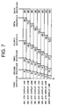
- Fig. 6 is a diagram showing an emission drive pattern based on the emission drive sequence shown in Fig. 5 and the pixel drive data GD.
- the following emission display is performed in accordance with the first grayscale drive.
- the column electrode drive circuit 5, row electrode Y drive circuit 7, row electrode X drive circuit 8 and drive control circuit 6 (hereafter called drive section) erase-discharge the discharge cells (indicated by black dots) in the address step W0 in the low-level subfields SF0 a and SF0 b , as shown in Fig. 6, in accordance with the pixel drive data GD of [110000], and set the discharge cells to light OFF mode.
- the following emission display is performed in accordance with the second grayscale drive.
- the drive section For the discharge cells belonging to the (8N-7)th display line, the drive section generates erase-discharge only in the low-level subfield SF1 a4 (indicated by a double circle) for the first half section and SF0 b (indicated by a black dot) in the latter half section within the unit display period. Therefore in this case, the discharge cells belonging to the (8N-7)th display line continuously perform sustain-discharge for emission in SF1 a1 to SF1 a4 (indicated by white circles and a double circle) which extend from initialization to light ON mode in the first low-level subfield SF0 a until generation of erase-discharge in SF1 a4 .
- the brightness level 8 corresponding to the overall length of the sustain-discharge for emission throughout the low-level subfields SF1 a1 to SF1 a4 is represented.
- the drive section For the discharge cells belonging to the (8N-6)th display line, the drive section generates erase-discharge in the low-level subfield SF0 a (indicated by a black dot) for the first half section and SF1 b4 (indicated by a double circle) in the latter half section within the unit display period.
- the discharge cells belonging to the (8N-6)th display line continuously perform sustain-discharge for emission in SF1 b1 to SF1 b4 (indicated by white circles and double circle) which extend from initialization to light ON mode in the low-level subfield SF0 b until generation of erase-discharge in SF1 b4 in the latter half section of the unit display period.
- the brightness level 7 corresponding to the overall length of the sustain-discharge for emission throughout the low-level subfields SF1 b1 to SF1 b4 is represented.
- the drive section For the discharge cells belonging to the (8N-5)th display line, the drive section generates erase-discharge in the low-level subfield SF1 a3 (indicated by a double circle) for the first half section and SF0 b (indicated by a black dot) in the latter half section within the unit display period. Therefore in this case, the discharge cells belonging to the (8N-5)th display line continuously perform sustain-discharge for emission in SF1 a1 to SF1 a3 (indicated by white circles and a double circle) which extend from initialization to light ON mode in the first low-level subfield SFO a until generation of erase-discharge in SF1 a3 .
- the drive section generates erase-discharge in the low-level subfield SFO a (indicated by a black dot) for the first half section and SF1 b3 (indicated by a double circle) in the latter half section within the unit display period.
- the discharge cells belonging to the (8N-4)th display line continuously perform sustain-discharge for emission in SF1 b1 to SF1 b3 (indicated by white circles and a double circle) which extend from initialization to light ON mode in the low-level subfield SF0 b until generation of erase-discharge in SF1 b3 in the latter half section of the unit display period.
- the brightness level 5 corresponding to the overall length of the sustain-discharge for emission throughout the low-level subfields SF1 b1 to SF1 b3 is represented.
- the drive section For the discharge cells belonging to the (8N-3)th display line, the drive section generates erase-discharge in the low-level subfield SF1 a2 (indicated by a double circle) for the first half section and SF0 b (indicated by a black dot) in the latter half section within the unit display period. Therefore in this case, the discharge cells belonging to the (8N-3)th display line continuously perform sustain-discharge for emission in SF1 a1 and SF1 a2 (indicated by a white circle and a double circle) which extend from initialization to light ON mode in the first low-level subfield SF0 a until generation of erase-discharge in SF1 a2 .
- the drive section For the discharge cells belonging to the (8N-2)th display line, the drive section generates erase-discharge in the low-level subfield SF0 a (indicated by a black dot) for the first half section and SF1 b2 (indicated by a double circle) in the latter half section within the unit display period.
- the discharge cells belonging to the (8N-2)th display line continuously perform sustain-discharge for emission in SF1 b1 and SF1 b2 (indicated by a white circle and a double circle) which extend from initialization to light ON mode in the low-level subfield SF0 b until generation of erase-discharge in SF1 b2 in the latter half section of the unit display period.
- the brightness level 3 corresponding to the overall length of the sustain-discharge for emission throughout the low-level subfields SF1 b1 and SF1 b2 is represented.
- the drive section For the discharge cells belonging to the (8N-1)th display line, the drive section generates erase-discharge in the low-level subfield SF1 a1 (indicated by a double circle) for the first half section and SF0 b (indicated by a black dot) in the latter half section within the unit display period. Therefore in this case, the discharge cells belonging to the (8N-1)th display line perform sustain-discharge emissions in the low-level subfield SF1 a1 (indicated by a double circle). By this operation, the brightness level 2 corresponding to the overall length of the sustain-discharge for emission in the low-level subfield SF1 a1 is represented.
- the drive section For the discharge cells belonging to the (8N)th display line, the drive section generates erase-discharge in the low-level subfield SF0 a (indicated by a black dot) for the first half section and SFl b1 (indicated by a double circle) in the latter half section within the unit display period. Therefore in this case, the discharge cells belonging to the (8N)th display line perform sustain-discharge emissions only in the low-level subfield SF1 b1 in the latter half section of the unit display period. By this operation, the brightness level 1 corresponding to the overall length of the sustain-discharge for emission in the low-level subfield SF1 b1 is represented.
- the following emission display is performed in accordance with the third grayscale drive described below.
- the drive section For the discharge cells belonging to the (8N-7)th display line, the drive section generates erase-discharge only in the low-level subfield SF1 a4 (indicated by a double circle) for the first half section and low-level subfield SF2 b4 (indicated by a double circle) in the latter half section within the unit display period. Therefore in this case, the discharge cells belonging to the (8N-7)th display line continuously perform sustain-discharge emissions in SF1 a1 to SF1 a4 (indicated by white circles and a double circle) for the first half section and SF1 b1 to SF2 b4 (indicated by white circles and a double circle) in the latter half section within the unit display period.
- the brightness level 24 corresponding to the overall length of the sustain-discharge for emission throughout the low-level subfields SF1 a1 to SF1 a4 and SF1 b1 to SF2 b4 is represented.
- the drive section For the discharge cells belonging to the (8N-6)th display line, the drive section generates erase-discharge only in the low-level subfield SF2 a4 (indicated by a double circle) for the first half section and low-level subfield SF1 b4 (indicated by a double circle) in the latter half section within the unit display period.
- the discharge cells belonging to the (8N-6)th display line continuously perform sustain-discharge for emission in SF1 a1 to SF2 a4 (indicated by white circles and a double circle) for the first half section and SF1 b1 to SF1 b4 (indicated by white circles and a double circle) in the latter half section within the unit display period.
- the brightness level 22 corresponding to the overall length of sustain-discharge for emission throughout the low-level subfields SF1 a1 to SF2 a4 and SF1 b1 to SF1 b4 is represented.
- the drive section For the discharge cells belonging to the (8N-5)th display line, the drive section generates erase-discharge only in the low-level subfields SF1 a3 (indicated by a double circle) for the first half section and low-level subfield SF2 b3 (indicated by a double circle) in the latter half section within the unit display period. Therefore in this case, the discharge cells belonging to the (8N-5)th display line continuously perform sustain-discharge for emission in SF1 a1 to SF1 a3 (indicated by white circles and a double circle) for the first half section and SF1 b1 to SF2 b3 (indicated by white circles and a double circle) in the latter half section within the unit display period.
- the brightness level 20 corresponding to the overall length of the sustain-discharge for emission throughout the low-level subfields SF1 a1 to SF1 a3 and SF1 b1 to SF2 b3 is represented.
- the drive section For the discharge cells belonging to the (8N-4)th display line, the drive section generates erase-discharge only in the low-level subfield SF2 a3 (indicated by a double circle) for the first half section and low-level subfield SF1 b3 (indicated by a double circle) in the latter half section within the unit display period.
- the discharge cells belonging to the (8N-4)th display line continuously perform sustain-discharge for emission in SF1 a1 to SF2 a3 (indicated by white circles and a double circle) for the first half section and SF1 b1 to SF1 b3 (indicated by white circles and a double circle) in the latter half section within the unit display period.
- the brightness level 18 corresponding to the overall length of sustain-discharge for emission throughout the low-level subfields SF1 a1 to SF2 a3 and SF1 b1 to SF1 b3 is represented.
- the drive section For the discharge cells belonging to the (8N-3)th display line, the drive section generates erase-discharge only in the low-level subfield SF1 a2 (indicated by a double circle) for the first half section and low-level subfield SF2 b2 (indicated by a double circle) in the latter half section within the unit display period. Therefore in this case, the discharge cells belonging to the (8N-3)th display line continuously perform sustain-discharge for emission in SF1 a1 and SF1 a2 (indicated by a white circle and a double circle) for the first half section and SF1 b1 to SF2 b2 (indicated by white circles and a double circle) in the latter half section within the unit display period.
- the drive section generates erase-discharge only in the low-level subfield SF2 a2 (indicated by a double circle) for the first half section and low-level subfield SF1 b2 (indicated by a double circle) in the latter half section within the unit display period.
- the discharge cells belonging to the (8N-2)th display line continuously performs sustain-discharge emissions in each of SF1 b1 to SF2 a2 (indicated by white circles and a double circle) for the first half section and SF1 b1 and SF1 b2 (indicated by a white circle and a double circle) in the latter half section within the unit display period.
- the brightness level 14 corresponding to the overall length of the sustain-discharge for emission throughout the low-level subfields SF1 a1 to SF2 a2 and SF1 b1 and SF1 b2 is represented.
- the drive section For the discharge cells belonging to the (8N-1)th display line, the drive section generates erase-discharge only in the low-level subfield SF1 a1 (indicated by a double circle) for the first half section and low-level subfield SF2 b1 (indicated by a double circle) in the latter half section within the unit display period. Therefore in this case, the discharge cells belonging to the (8N-1)th display line continuously perform sustain-discharge for emission in SF1 a1 (indicated by a double circle) for the first half section and SF1 b1 to SF2 b1 (indicated by white circles and a double circle) in the latter half section within the unit display period.
- the drive section generates erase-discharge only in the low-level subfield SF2 a1 (indicated by a double circle) for the first half section and low-level subfield SF1 b1 (indicated by a double circle) in the latter half section within the unit display period.
- the discharge cells belonging to the (8N)th display line continuously perform sustain-discharge for emission in SF1 a1 to SF2 a1 (indicated by white circles and a double circle) for the first half section and SF1 b1 in the latter half section within the unit display period.
- the brightness level 10 corresponding to the overall length of sustain-discharge for emission throughout the low-level subfields SF1 a1 to SF2 a1 and SF1 b1 is represented.
- the drive section For the discharge cells belonging to the (8N-7)th display line, the drive section generates erase-discharge only in the low-level subfield SF3 a4 (indicated by a double circle) for the first half section and low-level subfield SF2 b4 (indicated by a double circle) in the latter half section within the unit display period. Therefore in this case, the discharge cells belonging to the (8N-7)th display line continuously perform sustain-discharge for emission in SF1 a1 to SF3 a4 (indicated by white circles and a double circle) for the first half section and SF1 b1 to SF2 b4 (indicated by white circles and a double circle) in the latter half section within the unit display period.
- the brightness level 48 corresponding to the overall length of the sustain-discharge for emission throughout the low-level subfields SF1 a1 to SF3 a4 and SF1 b1 to SF2 b4 is represented.
- the drive section For the discharge cells belonging to the (8N-6)th display line, the drive section generates erase-discharge only in the low-level subfield SF2 a4 (indicated by a double circle) for the first half section and low-level subfield SF3 b4 (indicated by a double circle) in the latter half section within the unit display period.
- the discharge cells belonging to the (8N-6)th display line continuously perform sustain-discharge for emission in SF1 a1 to SF2 a4 (indicated by white circles and a double circle) for the first half section and SF1 b1 to SF3 b4 (indicated by white circles and a double circle) in the latter half section within the unit display period.
- the brightness level 45 corresponding to the overall length of sustain-discharge for emission throughout the low-level subfields SF1 a1 to SF2 a4 and SF1 b1 to SF3 b4 is represented.
- the drive section For the discharge cells belonging to the (8N-5)th display line, the drive section generates erase-discharge only in the low-level subfield SF3 a3 (indicated by a double circle) for the first half section and low-level subfield SF2 b3 (indicated by a double circle) in the latter half section within the unit display period. Therefore in this case, the discharge cells belonging to the (8N-5)th display line continuously perform sustain-discharge for emission in SF1 a1 to SF3 a3 (indicated by white circles and a double circle) for the first half section and SF1 b1 to SF2 b3 (indicated by white circles and a double circle) in the latter half section within the unit display period.
- the brightness level 42 corresponding to the overall length of the sustain-discharge for emission throughout the low-level subfields SF1 a1 to SF3 a3 and SF1 b1 to SF2 b3 is represented.
- the drive section For the discharge cells belonging to the (8N-4)th display line, the drive section generates erase-discharge only in the low-level subfield SF2 a3 (indicated by a double circle) for the first half section and low-level subfield SF3 b3 (indicated by a double circle) in the latter half section within the unit display period.
- the discharge cells belonging to the (8N-4)th display line continuously perform sustain-discharge for emission in SF1 a1 to SF2 a3 (indicated by white circles and a double circle) for the first half section and SF1 b1 to SF3 b3 (indicated by white circles and a double circle) in the latter half section within the unit display period.
- the brightness level 39 corresponding to the overall length of sustain-discharge for emission throughout the low-level subfields SF1 a1 to SF2 a3 and SF1 b1 to SF3 b3 is represented.
- the drive section For the discharge cells belonging to the (8N-3)th display line, the drive section generates erase-discharge only in the low-level subfield SF3 a2 (indicated by a double circle) for the first half section and low-level subfield SF2 b2 (indicated by a double circle) in the latter half section within the unit display period. Therefore in this case, the discharge cells belonging to the (8N-3)th display line continuously perform sustain-discharge for emission in SF1 a1 to SF3 a2 (indicated by white circles and a double circle) for the first half section and SF1 b1 to SF2 b2 (indicated by white circles and a double circle) in the latter half section within the unit display period.
- the brightness level 36 corresponding to the overall length of the sustain-discharge for emission throughout the low-level subfields SF1 a1 to SF3 a2 and SF1 b1 to SF2 b2 is represented.
- the drive section For the discharge cells belonging to the (8N-2)th display line, the drive section generates erase-discharge only in the low-level subfield SF2 a2 (indicated by a double circle) for the first half section and low-level subfield SF3 b2 (indicated by a double circle) in the latter half section within the unit display period.
- the discharge cells belonging to the (8N-2)th display line continuously perform sustain-discharge for emission in the SF1 a1 to SF2 a2 (indicated by white circles and a double circle) for the first half section and SF1 b1 to SF3 b2 (indicated by white circles and a double circle) in the latter half section within the unit display period.
- the brightness level 33 corresponding to the overall length of sustain-discharge for emission throughout the low-level subfields SF1 a1 to SF2 a2 and SF1 b1 to SF3 b2 is represented.
- the drive section For the discharge cells belonging to the (8N-1)th display line, the drive section generates erase-discharge only in the low-level subfield SF3 a1 (indicated by a double circle) for the first half section and low-level subfield SF2 b1 (indicated by a double circle) in the latter half section within the unit display period. Therefore in this case, the discharge cells belonging to the (8N-1)th display line continuously perform sustain-discharge for emission in SF1 a1 to SF3 a1 (indicated by white circles and a double circle) for the first half section and SF1 b1 to SF2 b1 (indicated by white circles and a double circle) in the latter half section within the unit display period.
- the brightness level 30 corresponding to the overall length of sustain-discharge for emission throughout the low-level subfields SF1 a1 to SF3 a1 and SF1 b1 to SF2 b1 is represented.
- the drive section For the discharge cells belonging to the (8N)th display line, the drive section generates erase-discharge only in the low-level subfield SF2 a1 (indicated by a double circle) for the first half section and low-level subfield SF3 b1 (indicated by a double circle) for the later half section in the unit display period.
- the discharge cells belonging to the (8N)th display line continuously perform sustain-discharge for emission in SF1 a1 to SF2 a1 (indicated by white circles and a double circle) for the first half section and SF1 b1 to SF3 b1 (indicated by white circles and a double circle) in the latter half section within the unit display period.
- the brightness level 27 corresponding to the overall length of the sustain-discharge for emission throughout the low-level subfields SF1 a1 to SF2 a1 and SF1 b1 to SF3 b1 is represented.
- the following emission display is performed in accordance with the fifth grayscale drive described below.
- the drive section For the discharge cells belonging to the (8N-7)th display line, the drive section generates erase-discharge only in the low-level subfield SF3 a4 (indicated by a double circle) for the first half section in the unit display period. Therefore in this case, the discharge cells belonging to the (8N-7)th display line continuously perform sustain-discharge for emission in SF1 a1 to SF3 a4 (indicated by white circles and a double circle) for the first half section and whole low-level subfields SF1 b1 to SF4 b4 (indicated by white circles) in the latter half section within the unit display period.
- the brightness level 80 corresponding to the overall length of the sustain-discharge for emission throughout the low-level subfields SF1 a1 to SF3 a4 and SF1 b1 to SF4 b4 is represented.
- the drive section For the discharge cells belonging to the (8N-6)th display line, the drive section generates erase-discharge only in the low-level subfield SF4 a4 (indicated by a double circle) for the first half section and low-level subfield SF3 b4 (indicated by a double circle) in the latter half section within the unit display period.
- the discharge cells belonging to the (8N-6)th display line continuously perform sustain-discharge for emission in SF1 a1 to SF4 a4 (indicated by white circles and a double circle) for the first half section and SF1 b1 to SF3 b4 (indicated by white circles and a double circle) in the latter half section within the unit display period.
- brightness level 76 corresponding to the overall length of the sustain-discharge for emission is represented.
- the drive section For the discharge cells belonging to the (8N-5)th display line, the drive section generates erase-discharge only in the low-level subfield SF3 a3 (indicated by a double circle) for the first half section and the low-level subfield SF4 b3 (indicated by a double circle) for the latter section in the unit display period. Therefore in this case, the discharge cells belonging to the (8N-5)th display line continuously perform sustain-discharge for emission in SF1 a1 to SF3 a3 (indicated by white circles and a double circle) for the first half section and SF1 b1 to SF4 b3 (indicated by white circles and a double circle) in the latter half section within the unit display period.
- the drive section For the discharge cells belonging to the (8N-4)th display line, the drive section generates erase-discharge only in the low-level subfield SF4 a3 (indicated by a double circle) for the first half section and low-level subfield SF3 b3 (indicated by a double circle) in the latter half section within the unit display period.
- the discharge cells belonging to the (8N-4)th display line continuously perform sustain-discharge for emission in SF1 a1 to SF4 a3 (indicated by white circles and a double circle) for the first half section and SF1 b1 to SF3 b3 (indicated by white circles and a double circle) in the latter half section within the unit display period.
- the brightness level 68 corresponding to the overall length of the sustain-discharge for emission is represented.
- the drive section For the discharge cells belonging to the (8N-3)th display line, the drive section generates erase-discharge only in the low-level subfield SF3 a2 (indicated by a double circle) for the first half section and the low-level subfield SF4 b2 (indicated by a double circle) in the latter half section within the unit display period. Therefore in this case, the discharge cells belonging to the (8N-3)th display line continuously perform sustain-discharge for emission in SF1 a1 to SF3 a2 (indicated by white circles and a double circle) for the first half section and SF1 b1 to SF4 b2 (indicated by white circles and a double circle) in the latter half section within the unit display period.
- the drive section For the discharge cells belonging to the (8N-2)th display line, the drive section generates erase-discharge only in the low-level subfield SF4 a2 (indicated by a double circle) for the first half section and low-level subfield SF3 b2 (indicated by a double circle) in the latter half section within the unit display period.
- the discharge cells belonging to the (8N-2)th display line continuously perform sustain-discharge for emission in SF1 a1 to SF4 a2 (indicated by white circles and a double circle) for the first half section and SF1 b1 to SF3 b2 (indicated by white circles and a double circle) in the latter half section within the unit display period.
- the brightness level 60 corresponding to the overall length of the sustain-discharge for emission is represented.
- the drive section For the discharge cells belonging to the (8N-1)th display line, the drive section generates erase-discharge only in the low-level subfield SF3 a1 (indicated by a double circle) for the first half section and low-level subfield SF4 b1 (indicated by a double circle) in the latter half section within the unit display period. Therefore in this case, the discharge cells belonging to the (8N-1)th display line continuously perform sustain-discharge for emission in SF1 a1 to SF3 a1 (indicated by white circles and a double circle) for the first half section and SF1 b1 to SF4 b1 (indicated by white circles and a double circle) in the latter half section within the unit display period.
- the drive section For the discharge cells belonging to the (8N)th display line, the drive section generates erase-discharge only in the low-level subfield SF4 a1 (indicated by a double circle) for the first half section and low-level subfield SF3 b1 (indicated by a double circle) in the latter half section within the unit display period.
- the discharge cells belonging to the (8N)th display line continuously perform sustain-discharge for emission in SF1 a1 to SF4 a1 (indicated by white circles and a double circle) for the first half section and SF1 b1 and SF3 b1 (indicated by white circles and a double circle) in the latter half section within the unit display period.
- the brightness level 52 corresponding to the overall length of the sustain-discharge for emission is represented.
- K denotes integers 3 and 4
- sustain-discharge for emission is performed by P subfields continuously placed in the first half section of the unit display period and by Q (Q ⁇ P) subfields continuously placed in the latter half section thereof.
- sustain-discharge for emission is performed by Q subfields continuously placed in the first half section of the unit display period and by P subfields continuously placed in the latter half section thereof.
- sustain-discharge for emission is performed by these M subfields similar to the above-described Kth grayscale display in the first half section of the unit display period, and by these Q subfields similar to the above-described Kth grayscale display and by L subsequent subfields in the latter half section thereof.
- emission is performed by these Q subfields similar to the above-described Kth grayscale display and by L subsequent subfields in the first half section of the unit display period, and by these P subfields similar to the above-described Kth grayscale display in the latter half section thereof.
- the number of subfields providing sustain-discharge for emission corresponding to the emission brightness in the first half section of the unit display period and the number of subfields providing sustain-discharge for emission corresponding to emission brightness in the latter half section thereof are switched or reversed between adjacent display lines.
- an emission display is performed as described below in accordance with the sixth grayscale drive so as to represent the highest brightness.
- the drive section in this case does not generate an erase-discharge at all on the discharge cells during the unit display period, and therefore sustain-discharge for emission are continuously performed throughout the low-level subfields from SF1 a1 to SF5 and from SF1 b1 to SF4 b4 .
- the highest brightness level 96 corresponding to the overall length of sustain-discharge for emission throughout the subfields is represented.
- the plasma display device shown in Fig. 3 performs the following line dither processing. Specifically, different line dither offset values LD are respectively assigned to a series of 8 display lines, that is:
- this line dither processing has two chances in the third to fifth grayscale drive to change the status of the discharge cell from light ON status to light OFF status within the unit display period (indicated by a double circle) as shown in Fig. 6.
- the frequency of the discharge cell switching from light ON status to light OFF status is twice as much as the vertical synchronizing frequency, a good display with suppressed flickers can be performed even if an input video signal with low vertical synchronizing frequency such as PAL type television signal is supplied.
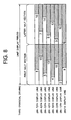
- sustain-discharge for emission is performed in both of the first half section and the latter half section of the unit display period for every grayscale in a manner that an emission period of one discharge cell belonging to one discharge line differs from that of another discharge cell belonging to another discharge line among a series of 8 discharge lines.
- relationship of the length of an emission period in the first half section to that in the latter half section is reversed between one discharge cell belonging to an even numbered display line and another discharge cell belonging to an odd numbered display line.
- sustain-discharge for emission with an emission period extending over 24 is performed separately by an emission period extending over 8 in the first half section and an emission period extending over 16 in the latter half section as shown in Fig. 8.
- sustain-discharge emission with an emission period extending over 22 is performed separately by an emission period extending over 15 in the first half section and an emission period extending over 7 in the latter half section, as shown in Fig. 8.
- the sustain-discharge emission with an emission period extending over 20 is performed separately by an emission period extending over 6 in the first half section and an emission period extending over 14 in the latter half section, as shown in Fig. 8.
- sustain-discharge emission with an emission period extending over 18 is performed separately by an emission period extending over 13 in the first half section and an emission period extending over 5 in the latter half section, as shown in Fig. 8.
- the sustain-discharge emission with an emission period extending over 16 is performed separately by an emission period extending over 4 in the first half section and an emission period extending over 12 in the latter half section, as shown in Fig. 8.
- sustain-discharge emission with an emission period extending over 14 is performed separately by an emission period extending over 11 in the first half section and an emission period extending over 3 in the latter half section, as shown in Fig. 8.
- sustain-discharge emission with an emission period extending over 12 is performed separately by an emission period extending over 2 in the first half section and an emission period extending over 10 in the latter half section, as shown in Fig. 8.
- sustain-discharge emission with an emission period extending over 10 is performed separately by an emission period extending over 9 in the first half section and an emission period extending over 1 in the latter half section, as shown in Fig. 8.
- emission patterns of a series of 8 display lines which are different from the line dither pattern corresponding to the brightness weight value fixedly assigned to the 8 display lines, differs to each other within a unit display period, and therefore the generation of a line dither pattern can be suppressed.
- a good image display with suppressed line dither patterns and flickers can be performed even if an input video signal with a low vertical synchronizing frequency is supplied.
- the relationship of the length of the emission period in the first half section to that in the and latter half section within the unit display period is reversed between one discharge cell belonging to an even numbered display line and another discharge cell belonging to an odd numbered display line, however above relationship may be reversed in a different manner.
- the relationship of the length of the emission period in the first half section to that in the latter half section within the unit display period may be reversed between adjacent display line units each having paired or tripled display lines, where such relationship are the same among display lines within each display line unit.
- a series of display lines may by arranged in a manner that one adjacent display line pair has such feature that relationship of the length of the emission period in the first half section to that in the latter half section within the unit display period is reversed between such adjacent display lines, whereas another adjacent display line pair has such feature that relationship of the length of the emission period in the first half section to that in the latter half section within the unit display period is the same between such adjacent display lines.
Landscapes
- Engineering & Computer Science (AREA)
- Physics & Mathematics (AREA)
- Computer Hardware Design (AREA)
- General Physics & Mathematics (AREA)
- Theoretical Computer Science (AREA)
- Power Engineering (AREA)
- Plasma & Fusion (AREA)
- Control Of Indicators Other Than Cathode Ray Tubes (AREA)
- Control Of Gas Discharge Display Tubes (AREA)
Abstract
Description
- The present invention relates to a method for driving a matrix display type display panel.
- Recently a plasma display panel (hereafter referred to as PDP) having a plurality of discharge cells arranged in a matrix pattern draws attention as a two-dimensional image display panel. On the other hand, a subfield method which displays an image corresponding to an input video signal on a PDP has been known. According to the subfield method, a display period of one field is divided into a plurality of subfields, and each of the discharge cells is selectively discharged for emission in each subfield in accordance with a brightness level indicated by the input video signal. By this operation, intermediate brightness corresponding to an overall emission period within one field period is visually recognized.
- Fig. 1 shows an example of an emission drive sequence based on the subfield method (see for example
Japanese Patent Application Laid-Open No. 2000-227778 - In the emission drive sequence shown in Fig. 1, one field period is divided into 14 subfields, i.e., subfields SF1 to SF14. Only in the first subfield SF1 among the subfields SF1 to SF14, all the discharge cells of the PDP are initialized into light ON mode (Rc). Further, in each of the subfields SF1 to SF14, a discharge cell is set to light OFF mode depending on the input video signal (Wc), and only a display cell set to light ON mode is discharged for emission during a period assigned to this subfield (Ic).
- Fig. 2 shows an example of an emission drive pattern within one field period of one discharge cell, which is driven based on such emission drive sequence (see for example
Japanese Patent Application Laid-Open No. 2000-227778 - According to the emission pattern in Fig. 2, a discharge cell which has been initialized to the light ON mode in the first subfield SF1 is selectively erase-discharged in one of the subfields SF1 to SF14 so as to set to light OFF mode as shown by black dots. A discharge cell which is once set to light OFF mode maintains its light OFF mode until the subfield SF14 at the very end. In other words, until being set to light OFF mode, a discharge cell is continuously discharged for emission in subfields shown by white circles from the first subfield SF1. Since each of the 15 types of emission patterns shown in Fig. 2 has a different total emission period in one field period, 15 types of intermediate brightness can be represented. In short, (N + 1) grayscales (N is the number of subfields) of intermediate brightness display is possible.
- In this method, however, the number of subfields into which one field is divided is limited, and therefore the number of grayscales may become insufficient. To compensate the insufficiency of the number of grayscales, multi-grayscale processing, such as error diffusion and dither processing, is performed for the input video signal.
- In error diffusion processing, the input video signal is converted into, for example, 8-bit pixel data for each pixel where the significant 6 bits thereof are recognized as the display data and the remaining insignificant 2 bits are recognized as error data. Error data corresponding to the peripheral pixels are respectively weighted and then added to each other so as to incorporate into the display data concerned. By this operation, the brightness of the insignificant 2 bits in an original pixel is artificially represented by the peripheral pixels, and therefore the grayscale representation of the brightness equivalent to the 8 bits of pixel data becomes possible by 6 bits of display data. Dither processing is then performed on the 6 bits of error diffusion-processed pixel data acquired by the above-described error diffusion processing. In the dither processing, a plurality of adjacent pixels are regarded as one pixel unit, and different dither coefficients are respectively assigned and added to the pixels in this one pixel unit where each of the pixels corresponds to the error diffusion-processed pixel data. By adding the dither coefficients, brightness equivalent to 8 bits can be represented only by the significant 4 bits of the dither-added pixel data in terms of one pixel unit. Accordingly, the significant 4 bits of the dither-added pixel data are extracted as the multi-grayscale pixel data Ds, and those data are respectively assigned to the 15 types of emission patterns, as shown in Fig. 2.
- However, when dither coefficients are regularly added to the pixel data by dither processing, a pseudo-pattern called a dither pattern, which is not related to the input video signal, may be visually recognized, which deteriorates image quality.
- Further, when the emission drive pattern shown in Fig. 2 is carried out, the switching from emission sustaining status to light OFF status is once or less within one field period, and therefore the switching frequency is the same as the vertical synchronizing frequency which determines one field display period. Therefore if a PAL type television signal, of which vertical synchronizing frequency is only 50 [Hz], is supplied as the input video signal, flickers tend to be outstanding.
- The present invention is provided to solve the foregoing problems, and an object of the present invention is to provide a method for driving a display panel which allows good image display where flickers and dither patterns are suppressed.
- According to a first aspect of the invention, there is provided a method for driving a display panel having a plurality of display lines each provided with a plurality of pixel cells, said pixel cells are driven by a plurality of subfields within each unit display period, said method comprising: a drive step for respectively assigning different brightness weight values to a series of M (M is an
integer 2 or higher) display lines belonging to each of display line groups, and for emitting said pixel cells based on said brightness weight values such that an emission period of a pixel cell belonging to one display line differs from that of another pixel cell belonging to another display line among said M display lines, wherein said drive step comprises a first half drive step for executing emission of a first period out of said emission period in a first half section of said unit display period, and a latter half drive step for executing emission of a remaining second period out of said emission period in a latter half section of said unit display period, and relationship of a length of said first period to a length of said second period is reversed between one pixel cell belonging to one display line and another pixel cell belonging to another display line among said display line group. - According to a second aspect of the invention, there is provided a method for driving a display panel having a plurality of display lines each provided with a plurality of pixel cells, said display panel is driven to display grayscale by a plurality of subfields in each unit display period in accordance with an input video signal, the method comprising: emitting one pixel cell belonging to one display line by P subfields (P is an integer) continuously placed in a first half section of said unit display period and by Q subfields (Q is an integer less than P) continuously placed in a latter half section of said unit display period, and emitting another pixel cell belonging to another display line adjacent to said one display line by Q subfields continuously placed in the first half section of said unit display period and by P subfields continuously placed in the latter half section of said unit display period, when the Kth grayscale display is performed, and emitting one pixel cell belonging to said one display line by said P subfields similara to said Kth grayscale display in the first half section of said unit display period, and by said Q subfields similar to said Kth grayscale display in the latter half section of said unit display period and by L subsequent subfields, and emitting said another pixel cell belonging to said another display line adjacent to said one display line by said P subfields similar to said Kth grayscale display and L subsequent subfields in the first half section of said unit display period, and by said P subfields similar to said Kth grayscale display, when (K+1)th grayscale is displayed.
-
- Fig. 1 is a diagram showing an example of an emission drive sequence based on the subfield method;
- Fig. 2 is a diagram showing an example of an emission drive pattern in one field period of one discharge cell which is driven based on the emission drive sequence shown in Fig. 1;
- Fig. 3 is a diagram showing a configuration of a plasma display device for driving a plasma display panel based on a driving method according to the present invention;
- Fig. 4 is a data conversion table in a drive
data conversion circuit 3 shown in Fig. 3; - Fig. 5 is a diagram showing an example of an emission drive sequence;
- Fig. 6 is a diagram showing an emission drive pattern based on the emission drive sequence shown in Fig. 5;
- Fig. 7 is a diagram showing a brightness level represented by a first to sixth grayscale drive for each display line; and
- Fig. 8 is a diagram showing an emission pattern in a unit display period by a third grayscale drive for each display line.
- A method for driving a display panel according to the present invention respectively assigns brightness weight values to a plurality of successive display lines belonging to each of display line groups. An emission period within a unit display period of one pixel cell belonging to one display line differs from that of another pixel cell belonging to another display line based on this brightness weight values. In this instance, the emission operation of the pixel cell during this emission period is separated into a first half section and a latter half section within a unit display period. Further, relationship of the length of an emission period in the first half section to that in the latter half section is reversed between one discharge cell belonging to one display line and another discharge cell belonging to another display line among the same display line group. According to this method, frequency to change the status of the discharge cell from light ON status to light OFF status is twice per a unit display period. Accordingly, a good display with suppressed flickers can be performed even if an input video signal with low vertical synchronizing frequency such as PAL type television signal is supplied. Further, emission patterns of a series of 8 display lines change in a unit display period in a manner different from the line dither pattern corresponding to the brightness weight values fixedly assigned to the 8 display lines, and therefore the generation of a line dither pattern can be suppressed.
- Embodiments of the present invention will be hereinafter described with reference to the drawings.
- Fig. 3 is a diagram showing a schematic configuration of a plasma display device for driving a plasma display panel according to the method of the present invention.
- In Fig. 3, the
PDP 100 as a plasma display panel has column electrodes D1 to Dm extending in the vertical direction, and row electrodes X1 to Xn and row electrodes Y1 to Yn extending in the horizontal direction of the two dimensional display screen. The row electrodes X1 to Xn and row electrodes Y1 to Yn are alternately arranged one by one. A pair of row electrodes X and Y, which are adjacent to each other, serve display of one display line in thePDP 100. Specifically, thePDP 100 has a first display line including row electrodes X1 and Y1, a second display line including row electrodes X2 and Y2, ... and an n-th display line including row electrodes Xn and Yn. A discharge space is provided between these first to n-th display lines and the column electrodes D1 to Dm so as to seal discharge gas therebetween, and a plurality of discharge cells each corresponding to a pixel are respectively formed at intersections between the row electrodes and the column electrodes including the discharge space. ThePDP 100 thus has (n × m) discharge cells G(1, 1) to G(n, m) which are arranged in a matrix pattern. - A pixel
data conversion circuit 1 converts an input video signal into pixel data PD of, for example, 8 bits which represents a brightness level of a pixel, and supplies the pixel data PD to amulti-grayscale processing circuit 2. It should be noted that the input video signal mentioned above is obtained after gamma correction on a source video signal corresponding to the image to be displayed. - The
multi-grayscale processing circuit 2 includes a line dither offsetvalue generation circuit 21,adder 22 and insignificant bit round-offcircuit 23. - The line dither offset
value generation circuit 21 first generates 8 line dither offset values LD respectively having the values of, for example, 0 through 7 such that these values respectively correspond to the following 8 display line sets, which are formed by dividing a first to n-th display lines of thePDP 100 in a manner that each of the sets is provided with a plurality of display lines of every eighth display line: - (8N-7)th display line set having {1st, 9th, 17th, ... (n-7)th display line},
- (8N-6)th display line set having (2nd, 10th, 18th, ... (n-6)th display line),
- (8N-5)th display line set having {3rd, 11th, 19th, ... (n-5)th display line},
- (8N-4)th display line set having {4th, 12th, 20th, ... (n-4)th display line},
- (8N-3)th display line set having {5th, 13th, 21th, ... (n-3)th display line},
- (8N-2)th display line set having {6th, 14th, 22th, ... (n-2)th display line},
- (8N-1)th display line set having (7th, 15th, 23th, ... (n-1)th display line}, and
- (8N)th display line set having {8th, 16th, 24th, ... nth display line},
- The line dither offset
value generation circuit 21 then supplies the line dither offset value LD to theadder 22 such that the line dither offset value LD corresponds to the display line which includes the discharge cell of the pixel data PD supplied from the pixeldata conversion circuit 1. - The
adder 22 supplies the line offset added pixel data LF, which is obtained by addition of the line dither offset value LD with the pixel data PD, to an insignificant bit round-off circuit 23. The insignificant bit round-off circuit 23 rounds off the insignificant 3 bits of the line offset added pixel data LF, and supplies the remaining significant 3 bits to a drivedata conversion circuit 3 as multi-grayscale pixel data MD. - The drive
data conversion circuit 3 converts the 3 bit multi-grayscale pixel data MD to 6 bit pixel drive data GD in accordance with a data conversion table shown in Fig. 4, and supplies it to amemory 4. - The
memory 4 sequentially receives and stores the pixel drive data GD of each pixel. Upon completion of the writing of pixel drive data GD1, 1 to GDn, m of one image frame (n rows × m columns), thememory 4 separates each of the pixel drive data GD1, 1 to GDn, m into bit digits, and reads one display line at a time. Thememory 4 reads pixel drive data bits of the one display line (m bits), and supplies them to a columnelectrode drive circuit 5 as the pixel drive data bits DB1 to DB(m). - The
drive control circuit 6 generates various timing signals for grayscale driving thePDP 100 in accordance with the emission drive sequence shown in Fig. 5, and supplies them to the columnelectrode drive circuit 5, row electrodeY drive circuit 7 and row electrodeX drive circuit 8 respectively. Each of the columnelectrode drive circuit 5, row electrodeY drive circuit 7 and row electrodeX drive circuit 8 generates various drive pulses (not shown) for driving thePDP 100 as described below in response to a timing signal supplied from thedrive control circuit 6, and applies them to the column electrodes D1 to Dm, row electrodes X1 to Xn and row electrodes Y1 to Yn of thePDP 100. - In the emission drive sequence shown in Fig. 5, the following six subfields SF0 to SF5 are used so as to represent the various brightness levels for displaying one frame or one field of image in six levels.
- The subfield SF0 determines whether the
lowest brightness level 0 is represented or a higher brightness level is represented. The subfield SF0 is comprised of a low-level subfield SF0a placed in the beginning of the first half section of a unit display period, i.e., one frame or one field display period, and a low-level subfield SF0b placed in the beginning of the latter half section thereof, as shown in Fig. 5. In each of the low-level subfields SF0a and SF0b, thedrive control circuit 6 executes a reset step R for initializing all the discharge cells to light ON mode status, where a predetermined amount of wall charges are formed, and an address step W0 for selectively erase-discharging discharge cells depending on the pixel drive data GD from the first to n-th display lines of thePDP 100 in a manner that each display line is erase-discharged at a time. - The subfield SF1 serves to provide emission with higher brightness level than the
lowest brightness level 0 by only one level. The subfield SF1 is comprised of 8 low-level subfields SF1a1 to SF1a4 and SF1b1 to SF1b4, as shown in Fig. 5, so as to differentiate a brightness level of emission of one discharge cell belonging to one display line from that of another discharge cell belonging to another display line among 8 display lines of each display line group. In this case, as shown in Fig. 5, 4 low-level subfields SF1a1 to SF1a4, out of these 8 low-level subfields, are placed after the low-level subfield SF0a in the first half section of the unit display period, and the remaining low-level subfields SF1b1 to SF1b4 are placed after the low-level subfield SF0b in the latter half section of the unit display period. In the low-level subfield SF1a1, thedrive control circuit 6 sequentially executes the sustain step I for repeatedly sustain-discharging the display cells which are set to light ON mode, during a period extending over 2, and the address step W7 for selectively erase-discharging only the discharge cells placed in the (8N-1)th display line in accordance with the pixel drive data GD. In the low-level subfield SF1a2, thedrive control circuit 6 sequentially executes the sustain step I for repeatedly sustain-discharging the discharge cells which are set to light ON mode, during a period extending over 2, and the address step W5 for selectively erase-discharging only the discharge cells placed in the (8N-3)th display line in accordance with the pixel drive data GD. In the low-level subfield SF1a3, thedrive control circuit 6 sequentially executes the sustain step I for repeatedly sustain-discharging the discharge cells which are set to light ON mode, during a period extending over 2, and the address step W3 for selectively erase-discharging only the discharge cells placed in the (8N-5)th display line in accordance with the pixel drive data GD. In the low-level subfield SF1a4, thedrive control circuit 6 sequentially executes the sustain step I for repeatedly sustain-discharging the discharge cells which are set to light ON mode, during a period extending over 2, and the address step W1 for selectively erase-discharging only the discharge cells placed in the (8N-7)th display line in accordance with the pixel drive data GD. In the low-level subfield SF1b1, thedrive control circuit 6 sequentially executes the sustain step I for repeatedly sustain-discharging the discharge cells which are set to light ON mode, during a period extending over 1, and the address step W8 for selectively erase-discharging only the discharge cells placed in the (8N)th display line in accordance with the pixel drive data GD. In the low-level subfield SF1b2, thedrive control circuit 6 sequentially executes the sustain step I for repeatedly sustain-discharging the discharge cells which are set to light ON mode, during a period extending over 2, and the address step W6 for selectively erase-discharging only the discharge cells placed in the (8N-2)th display line in accordance with the pixel drive data GD. In the low-level subfield SF1b3, thedrive control circuit 6 sequentially executes the sustain step I for repeatedly sustain-discharging the discharge cells which are set to light ON mode, during a period extending over 2, and the address step W4 for selectively erase-discharging only the discharge cells placed in the (8N-4)th display line in accordance with the pixel drive data GD. In the low-level subfield SF1b4, thedrive control circuit 6 sequentially executes the sustain step I for repeatedly sustain-discharging the discharge cells which are set to light ON mode, during a period extending over 2, and the address step W2 for selectively erase-discharging only the discharge cells placed in the (8N-6)th display line in accordance with the pixel drive data GD. - The subfield SF2 serves to provide emission with higher brightness level than the subfield SF1 by only one level. The subfield SF2 is comprised of 8 low-level subfields SF2a1 to SF2a4 and SF2b1 to SF2b4, as shown in Fig. 5, so as to differentiate a brightness level of emission of one discharge cell belonging to one display line from that of another discharge cell belonging to another display line among 8 display lines of each display line group. In this case, as Fig. 5 shows, 4 low-level subfields SF2a1 to SF2a4, out of these 8 low-level subfields, are placed after the low-level subfield SF1a4 in the first half section of the unit display period, and the remaining low-level subfields SF2b1 to SF2b4 are placed after the low-level subfield SF1b4 in the latter half section of the unit display period. In the low-level subfield SF2a1, the
drive control circuit 6 sequentially executes the sustain step I for repeatedly sustain-discharging the discharge cells which are set to light ON mode, during a period extending over 1, and the address step W8 for selectively erase-discharging only the discharge cells placed in the (8N)th display line in accordance with the pixel drive data GD. In the low-level subfield SF2a2, thedrive control circuit 6 sequentially executes the sustain step I for repeatedly sustain-discharging the discharge cells which are set to light ON mode, during a period extending over 2, and the address step W6 for selectively erase-discharging only the discharge cells placed in the (8N-2)th display line in accordance with the pixel drive data GD. In the low-level subfield SF2a3, thedrive control circuit 6 sequentially executes the sustain step I for repeatedly sustain-discharging the discharge cells which are set to light ON mode, during a period extending over 2, and the address step W4 for selectively erase-discharging only the discharge cells placed in the (8N-4)th display line in accordance with the pixel drive data GD. In the low-level subfield SF2a4, thedrive control circuit 6 sequentially executes the sustain step I for repeatedly sustain-discharging the discharge cells which are set to light ON mode, during a period extending over 2, and the address step W2 for selectively erase-discharging only the discharge cells placed in the (8N-6)th display line in accordance with the pixel drive data GD. In the low-level subfield SF2b1, thedrive control circuit 6 sequentially executes the sustain step I for repeatedly sustain-discharging the discharge cells which are set to light ON mode, during a period extending over 3, and the address step W7 for selectively erase-discharging only the discharge cells placed in the (8N-1)th display line in accordance with the pixel drive data GD. In the low-level subfield SF2b2, thedrive control circuit 6 sequentially executes the sustain step I for repeatedly sustain-discharging the discharge cells which are set to light ON mode, during a period extending over 2, and the address step W5 for selectively erase-discharging only the discharge cells placed in the (8N-3)th display line in accordance with the pixel drive data GD. In the low-level subfield SF2b3, thedrive control circuit 6 sequentially executes the sustain step I for repeatedly sustain-discharging the discharge cells which are set to light ON mode, during a period extending over 2, and the address steps W3 for selectively erase-discharging only the discharge cells placed in the (8N-5)th display line according to the pixel data GD. In the low-level subfield SF2b4, thedrive control circuit 6 sequentially executes the sustain step I for repeatedly sustain-discharging the discharge cells which are set to light ON mode, during a period extending over 2, and the address step W1 for selectively erase-discharging only the discharge cells placed in the (8N-7)th display line in accordance with the pixel drive data GD. - The subfield SF3 serves to provide emission with higher brightness than the subfield SF2 by only one level. The subfield SF3 is comprised of 8 low-level subfields SF3a1 to SF3a4 and SF3b1 to SF3b4, as shown in Fig. 5, so as to differentiate a brightness level of emission of one discharge cell belonging to one display line from that of another discharge cell belonging to another display line among 8 display lines of each display line group. In this case, as Fig. 5 shows, 4 low-level subfields SF3a1 to SF3a4, out of these 8 low-level subfields, are placed after the low-level subfield SF2a4 in the first half section of the unit display period, and the remaining low-level subfields SF3b1 to SF3b4 are placed after the low-level subfield SF2b4 in the latter half section of the unit display period. In the low-level subfield SF3a1, the
drive control circuit 6 sequentially executes the sustain step I for repeatedly sustain-discharging the discharge cells which are set to light ON mode, during a period extending over 5, and the address step W7 for selectively erase-discharging only the discharge cells placed in the (8N-1)th display line in accordance with the pixel drive data GD. In the low-level subfield SF3a2, thedrive control circuit 6 sequentially executes the sustain step I for repeatedly sustain-discharging the discharge cells which are set to light ON mode, during a period extending over 4, and the address step W5 for selectively erase-discharging only the discharge cells placed in the (8N-3)th display line in accordance with the pixel drive data GD. In the low-level subfield SF3a3, thedrive control circuit 6 sequentially executes the sustain step I for repeatedly sustain-discharging the discharge cells which are set to light ON mode, during a period extending over 4, and the address step W3 for selectively erase-discharging only the discharge cells placed in the (8N-5)th display line in accordance with the pixel drive data GD. In the low-level subfield SF3a4, thedrive control circuit 6 sequentially executes the sustain step I for repeatedly sustain-discharging the discharge cells which are set to light ON mode, during a period extending over 4, and the address step W1 for selectively erase-discharging only the discharge cells placed in the (8N-7)th display line in accordance with the pixel drive data GD. In the low-level subfield SF3b1, thedrive control circuit 6 sequentially executes the sustain step I for repeatedly sustain-discharging the discharge cells which are set to light ON mode, during a period extending over 2, and the address step W8 for selectively erase-discharging only the discharge cells placed in the (8N)th display line in accordance with the pixel drive data GD. In the low-level subfield SF3b2, thedrive control circuit 6 sequentially executes the sustain step I for repeatedly sustain-discharging the discharge cells which are set to light ON mode, during a period extending over 4, and the address step W6 for selectively erase-discharging only the discharge cells placed in the (8N-2)th display line in accordance with the pixel drive data GD. In the low-level subfield SF3b3, thedrive control circuit 6 sequentially executes the sustain step I for repeatedly sustain-discharging the discharge cells which are set to light ON mode, during a period extending over 4, and the address step W4 for selectively erase-discharging only the discharge cells placed in the (8N-4)th display line in accordance with the pixel drive data GD. In the low-level subfield SF3b4, thedrive control circuit 6 sequentially executes the sustain step I for repeatedly sustain-discharging the discharge cells which are set to light ON mode, during a period extending over 4, and the address step W2 for selectively erase-discharging only the discharge cells placed in the (8N-6)th display line in accordance with the pixel drive data GD. - The subfield SF4 serves to provide emission with higher brightness level than the subfield SF3 by only one level. The subfield SF4 is comprised of 8 low-level subfields SF4a1 to SF4a4 and SF4b1 to SFb4b, as shown in Fig. 5, so as to differentiate a brightness level of emission of one discharge cell belonging to one display line from that of another discharge cell belonging to another display line among 8 display lines of each display line group. In this case, as Fig. 5 shows, 4 low-level subfields SF4a1 to SF4a4, out of these 8 low-level subfields, are placed after the low-level subfield SF3a4 in the first half section of the unit display period, and the remaining low-level subfields SF4b1 to SF4b4 are placed after the low-level subfield SF3b4 in the latter half section of the unit display period. In the low-level subfield SF4a1, the
drive control circuit 6 sequentially executes the sustain step I for repeatedly sustain-discharging the discharge cells which are set to light ON mode, during a period extending over 2, and the address step W8 for selectively erase-discharging only the discharge cells placed in the (8N)th display line in accordance with the pixel drive data GD. In the low-level subfield SF4a2, thedrive control circuit 6 sequentially executes the sustain step I for repeatedly sustain-discharging the discharge cells which are set to light ON mode, during a period extending over 4, and the address step W6 for selectively erase-discharging only the discharge cells placed in the (8N-2)th display line in accordance with the pixel drive data GD. In the low-level subfield SF4a3, thedrive control circuit 6 sequentially executes the sustain step I for repeatedly sustain-discharging the discharge cells which are set to light ON mode, during a period extending over 4, and the address step W4 for selectively erase-discharging only the discharge cells placed in the (8N-4)th display line in accordance with the pixel drive data GD. In the low-level subfield SF4a4, thedrive control circuit 6 sequentially executes the sustain step I for repeatedly sustain-discharging the discharge cells which are set to light ON mode, during a period extending over 4, and the address step W2 for selectively erase-discharging only the discharge cells placed in the (8N-6)th display line in accordance with the pixel drive data GD. In the low-level subfield SF4b1, thedrive control circuit 6 sequentially executes the sustain step I for repeatedly sustain-discharging the discharge cells which are set to light ON mode, during a period extending over 6, and the address step W7 for selectively erase-discharging only the discharge cells placed in the (8N-1)th display line in accordance with the pixel drive data GD. In the low-level subfield SF4b2, thedrive control circuit 6 sequentially executes the sustain step I for repeatedly sustain-discharging the discharge cells which are set to light ON mode, during a period extending over 4, and the address step W5 for selectively erase-discharging only the discharge cells placed in the (8N-3)th display line in accordance with the pixel drive data GD. In the low-level subfield SF4b3, thedrive control circuit 6 sequentially executes the sustain step I for repeatedly sustain-discharging the discharge cells which are set to light ON mode, during a period extending over 4, and the address step W3 for selectively erase-discharging only the discharge cells placed in the (8N-5)th display line in accordance with the pixel drive data GD. In the low-level subfield SF4b4, thedrive control circuit 6 executes the sustain step I for repeatedly sustain-discharging the discharge cells which are set to light On mode during a period extending over 4. - The subfield SF5 serves to provide emission with higher brightness level than the subfield SF4 by only one level, and is placed only at the very end of the first half section of the unit display period. In the subfield SF5, the
drive control circuit 6 executes the sustain step I for repeatedly sustain-discharging the discharge cells which are set to light ON mode during a period extending over 2. - Fig. 6 is a diagram showing an emission drive pattern based on the emission drive sequence shown in Fig. 5 and the pixel drive data GD.
- First, according to the pixel drive data GD of [110000] indicating lowest brightness, the following emission display is performed in accordance with the first grayscale drive. Specifically, the column
electrode drive circuit 5, row electrodeY drive circuit 7, row electrodeX drive circuit 8 and drive control circuit 6 (hereafter called drive section) erase-discharge the discharge cells (indicated by black dots) in the address step W0 in the low-level subfields SF0a and SF0b, as shown in Fig. 6, in accordance with the pixel drive data GD of [110000], and set the discharge cells to light OFF mode. According to the driving shown in Fig. 5, the chances to shift discharge cells to light ON mode in the unit display period are only the reset steps R in low-level subfields SF0a and SF0b. Therefore, in the case of the first grayscale drive in accordance with the pixel drive data GD of [110000], all discharge cells maintain light OFF mode throughout the unit display period, and display withbrightness level 0 is performed. - According to the pixel drive data GD of [011000] indicating higher brightness than the above-described [110000] by only one level, the following emission display is performed in accordance with the second grayscale drive.
- Specifically, for the discharge cells belonging to the (8N-7)th display line, the drive section generates erase-discharge only in the low-level subfield SF1a4 (indicated by a double circle) for the first half section and SF0b (indicated by a black dot) in the latter half section within the unit display period. Therefore in this case, the discharge cells belonging to the (8N-7)th display line continuously perform sustain-discharge for emission in SF1a1 to SF1a4 (indicated by white circles and a double circle) which extend from initialization to light ON mode in the first low-level subfield SF0a until generation of erase-discharge in SF1a4. By this operation, the
brightness level 8 corresponding to the overall length of the sustain-discharge for emission throughout the low-level subfields SF1a1 to SF1a4 is represented. For the discharge cells belonging to the (8N-6)th display line, the drive section generates erase-discharge in the low-level subfield SF0a (indicated by a black dot) for the first half section and SF1b4 (indicated by a double circle) in the latter half section within the unit display period. Therefore in this case, the discharge cells belonging to the (8N-6)th display line continuously perform sustain-discharge for emission in SF1b1 to SF1b4 (indicated by white circles and double circle) which extend from initialization to light ON mode in the low-level subfield SF0b until generation of erase-discharge in SF1b4 in the latter half section of the unit display period. By this operation, thebrightness level 7 corresponding to the overall length of the sustain-discharge for emission throughout the low-level subfields SF1b1 to SF1b4 is represented. For the discharge cells belonging to the (8N-5)th display line, the drive section generates erase-discharge in the low-level subfield SF1a3 (indicated by a double circle) for the first half section and SF0b (indicated by a black dot) in the latter half section within the unit display period. Therefore in this case, the discharge cells belonging to the (8N-5)th display line continuously perform sustain-discharge for emission in SF1a1 to SF1a3 (indicated by white circles and a double circle) which extend from initialization to light ON mode in the first low-level subfield SFOa until generation of erase-discharge in SF1a3. By this operation, thebrightness level 6 corresponding to the overall length of the sustain-discharge for emission throughout the low-level subfields SF1a1 to SF1a3 is represented. For the discharge cells belonging to the (8N-4)th display line, the drive section generates erase-discharge in the low-level subfield SFOa (indicated by a black dot) for the first half section and SF1b3 (indicated by a double circle) in the latter half section within the unit display period. Therefore in this case, the discharge cells belonging to the (8N-4)th display line continuously perform sustain-discharge for emission in SF1b1 to SF1b3 (indicated by white circles and a double circle) which extend from initialization to light ON mode in the low-level subfield SF0b until generation of erase-discharge in SF1b3 in the latter half section of the unit display period. By this operation, thebrightness level 5 corresponding to the overall length of the sustain-discharge for emission throughout the low-level subfields SF1b1 to SF1b3 is represented. For the discharge cells belonging to the (8N-3)th display line, the drive section generates erase-discharge in the low-level subfield SF1a2 (indicated by a double circle) for the first half section and SF0b (indicated by a black dot) in the latter half section within the unit display period. Therefore in this case, the discharge cells belonging to the (8N-3)th display line continuously perform sustain-discharge for emission in SF1a1 and SF1a2 (indicated by a white circle and a double circle) which extend from initialization to light ON mode in the first low-level subfield SF0a until generation of erase-discharge in SF1a2. By this operation, thebrightness level 4 corresponding to the overall length of the sustain-discharge for emission throughout the low-level subfields SF1a1 and SF1a2 is represented. For the discharge cells belonging to the (8N-2)th display line, the drive section generates erase-discharge in the low-level subfield SF0a (indicated by a black dot) for the first half section and SF1b2 (indicated by a double circle) in the latter half section within the unit display period. Therefore in this case, the discharge cells belonging to the (8N-2)th display line continuously perform sustain-discharge for emission in SF1b1 and SF1b2 (indicated by a white circle and a double circle) which extend from initialization to light ON mode in the low-level subfield SF0b until generation of erase-discharge in SF1b2 in the latter half section of the unit display period. By this operation, thebrightness level 3 corresponding to the overall length of the sustain-discharge for emission throughout the low-level subfields SF1b1 and SF1b2 is represented. For the discharge cells belonging to the (8N-1)th display line, the drive section generates erase-discharge in the low-level subfield SF1a1 (indicated by a double circle) for the first half section and SF0b (indicated by a black dot) in the latter half section within the unit display period. Therefore in this case, the discharge cells belonging to the (8N-1)th display line perform sustain-discharge emissions in the low-level subfield SF1a1 (indicated by a double circle). By this operation, thebrightness level 2 corresponding to the overall length of the sustain-discharge for emission in the low-level subfield SF1a1 is represented. For the discharge cells belonging to the (8N)th display line, the drive section generates erase-discharge in the low-level subfield SF0a (indicated by a black dot) for the first half section and SFlb1 (indicated by a double circle) in the latter half section within the unit display period. Therefore in this case, the discharge cells belonging to the (8N)th display line perform sustain-discharge emissions only in the low-level subfield SF1b1 in the latter half section of the unit display period. By this operation, thebrightness level 1 corresponding to the overall length of the sustain-discharge for emission in the low-level subfield SF1b1 is represented. - According to the pixel drive data GD of [001100] indicating higher brightness than the above-described [011000] by only one level, the following emission display is performed in accordance with the third grayscale drive described below.
- Specifically, for the discharge cells belonging to the (8N-7)th display line, the drive section generates erase-discharge only in the low-level subfield SF1a4 (indicated by a double circle) for the first half section and low-level subfield SF2b4 (indicated by a double circle) in the latter half section within the unit display period. Therefore in this case, the discharge cells belonging to the (8N-7)th display line continuously perform sustain-discharge emissions in SF1a1 to SF1a4 (indicated by white circles and a double circle) for the first half section and SF1b1 to SF2b4 (indicated by white circles and a double circle) in the latter half section within the unit display period. By this operation, the
brightness level 24 corresponding to the overall length of the sustain-discharge for emission throughout the low-level subfields SF1a1 to SF1a4 and SF1b1 to SF2b4 is represented. For the discharge cells belonging to the (8N-6)th display line, the drive section generates erase-discharge only in the low-level subfield SF2a4 (indicated by a double circle) for the first half section and low-level subfield SF1b4 (indicated by a double circle) in the latter half section within the unit display period. Therefore in this case, the discharge cells belonging to the (8N-6)th display line continuously perform sustain-discharge for emission in SF1a1 to SF2a4 (indicated by white circles and a double circle) for the first half section and SF1b1 to SF1b4 (indicated by white circles and a double circle) in the latter half section within the unit display period. By this operation, thebrightness level 22 corresponding to the overall length of sustain-discharge for emission throughout the low-level subfields SF1a1 to SF2a4 and SF1b1 to SF1b4 is represented. For the discharge cells belonging to the (8N-5)th display line, the drive section generates erase-discharge only in the low-level subfields SF1a3 (indicated by a double circle) for the first half section and low-level subfield SF2b3 (indicated by a double circle) in the latter half section within the unit display period. Therefore in this case, the discharge cells belonging to the (8N-5)th display line continuously perform sustain-discharge for emission in SF1a1 to SF1a3 (indicated by white circles and a double circle) for the first half section and SF1b1 to SF2b3 (indicated by white circles and a double circle) in the latter half section within the unit display period. By this operation, thebrightness level 20 corresponding to the overall length of the sustain-discharge for emission throughout the low-level subfields SF1a1 to SF1a3 and SF1b1 to SF2b3 is represented. For the discharge cells belonging to the (8N-4)th display line, the drive section generates erase-discharge only in the low-level subfield SF2a3 (indicated by a double circle) for the first half section and low-level subfield SF1b3 (indicated by a double circle) in the latter half section within the unit display period. Therefore in this case, the discharge cells belonging to the (8N-4)th display line continuously perform sustain-discharge for emission in SF1a1 to SF2a3 (indicated by white circles and a double circle) for the first half section and SF1b1 to SF1b3 (indicated by white circles and a double circle) in the latter half section within the unit display period. By this operation, thebrightness level 18 corresponding to the overall length of sustain-discharge for emission throughout the low-level subfields SF1a1 to SF2a3 and SF1b1 to SF1b3 is represented. For the discharge cells belonging to the (8N-3)th display line, the drive section generates erase-discharge only in the low-level subfield SF1a2 (indicated by a double circle) for the first half section and low-level subfield SF2b2 (indicated by a double circle) in the latter half section within the unit display period. Therefore in this case, the discharge cells belonging to the (8N-3)th display line continuously perform sustain-discharge for emission in SF1a1 and SF1a2 (indicated by a white circle and a double circle) for the first half section and SF1b1 to SF2b2 (indicated by white circles and a double circle) in the latter half section within the unit display period. By this operation, thebrightness level 16 corresponding to the overall length of sustain-discharge for emission throughout the low-level subfields SF1a1 and SF1a2, and SF1b1 to SF2b2 is represented. For the discharge cells belonging to the (8N-2)th display line, the drive section generates erase-discharge only in the low-level subfield SF2a2 (indicated by a double circle) for the first half section and low-level subfield SF1b2 (indicated by a double circle) in the latter half section within the unit display period. Therefore in this case, the discharge cells belonging to the (8N-2)th display line continuously performs sustain-discharge emissions in each of SF1b1 to SF2a2 (indicated by white circles and a double circle) for the first half section and SF1b1 and SF1b2 (indicated by a white circle and a double circle) in the latter half section within the unit display period. By this operation, thebrightness level 14 corresponding to the overall length of the sustain-discharge for emission throughout the low-level subfields SF1a1 to SF2a2 and SF1b1 and SF1b2 is represented. For the discharge cells belonging to the (8N-1)th display line, the drive section generates erase-discharge only in the low-level subfield SF1a1 (indicated by a double circle) for the first half section and low-level subfield SF2b1 (indicated by a double circle) in the latter half section within the unit display period. Therefore in this case, the discharge cells belonging to the (8N-1)th display line continuously perform sustain-discharge for emission in SF1a1 (indicated by a double circle) for the first half section and SF1b1 to SF2b1 (indicated by white circles and a double circle) in the latter half section within the unit display period. By this operation, thebrightness level 12 corresponding to the overall length of the sustain-discharge for emission throughout the low-level subfields SF1a1 and SF1b1 to SF2b1 is represented. For the discharge cells belonging to the (8N)th display line, the drive section generates erase-discharge only in the low-level subfield SF2a1 (indicated by a double circle) for the first half section and low-level subfield SF1b1 (indicated by a double circle) in the latter half section within the unit display period. Therefore in this case, the discharge cells belonging to the (8N)th display line continuously perform sustain-discharge for emission in SF1a1 to SF2a1 (indicated by white circles and a double circle) for the first half section and SF1b1 in the latter half section within the unit display period. By this operation, thebrightness level 10 corresponding to the overall length of sustain-discharge for emission throughout the low-level subfields SF1a1 to SF2a1 and SF1b1 is represented. - Accordance to the pixel drive data GD of [000110] indicating higher brightness than the above-described [001100] by only one level, the following emission display is performed in accordance with the fourth grayscale drive described below.
- Specifically, for the discharge cells belonging to the (8N-7)th display line, the drive section generates erase-discharge only in the low-level subfield SF3a4 (indicated by a double circle) for the first half section and low-level subfield SF2b4 (indicated by a double circle) in the latter half section within the unit display period. Therefore in this case, the discharge cells belonging to the (8N-7)th display line continuously perform sustain-discharge for emission in SF1a1 to SF3a4 (indicated by white circles and a double circle) for the first half section and SF1b1 to SF2b4 (indicated by white circles and a double circle) in the latter half section within the unit display period. By this operation, the
brightness level 48 corresponding to the overall length of the sustain-discharge for emission throughout the low-level subfields SF1a1 to SF3a4 and SF1b1 to SF2b4 is represented. For the discharge cells belonging to the (8N-6)th display line, the drive section generates erase-discharge only in the low-level subfield SF2a4 (indicated by a double circle) for the first half section and low-level subfield SF3b4 (indicated by a double circle) in the latter half section within the unit display period. Therefore in this case, the discharge cells belonging to the (8N-6)th display line continuously perform sustain-discharge for emission in SF1a1 to SF2a4 (indicated by white circles and a double circle) for the first half section and SF1b1 to SF3b4 (indicated by white circles and a double circle) in the latter half section within the unit display period. By this operation, thebrightness level 45 corresponding to the overall length of sustain-discharge for emission throughout the low-level subfields SF1a1 to SF2a4 and SF1b1 to SF3b4 is represented. For the discharge cells belonging to the (8N-5)th display line, the drive section generates erase-discharge only in the low-level subfield SF3a3 (indicated by a double circle) for the first half section and low-level subfield SF2b3 (indicated by a double circle) in the latter half section within the unit display period. Therefore in this case, the discharge cells belonging to the (8N-5)th display line continuously perform sustain-discharge for emission in SF1a1 to SF3a3 (indicated by white circles and a double circle) for the first half section and SF1b1 to SF2b3 (indicated by white circles and a double circle) in the latter half section within the unit display period. By this operation, thebrightness level 42 corresponding to the overall length of the sustain-discharge for emission throughout the low-level subfields SF1a1 to SF3a3 and SF1b1 to SF2b3 is represented. For the discharge cells belonging to the (8N-4)th display line, the drive section generates erase-discharge only in the low-level subfield SF2a3 (indicated by a double circle) for the first half section and low-level subfield SF3b3 (indicated by a double circle) in the latter half section within the unit display period. Therefore in this case, the discharge cells belonging to the (8N-4)th display line continuously perform sustain-discharge for emission in SF1a1 to SF2a3 (indicated by white circles and a double circle) for the first half section and SF1b1 to SF3b3 (indicated by white circles and a double circle) in the latter half section within the unit display period. By this operation, thebrightness level 39 corresponding to the overall length of sustain-discharge for emission throughout the low-level subfields SF1a1 to SF2a3 and SF1b1 to SF3b3 is represented. For the discharge cells belonging to the (8N-3)th display line, the drive section generates erase-discharge only in the low-level subfield SF3a2 (indicated by a double circle) for the first half section and low-level subfield SF2b2 (indicated by a double circle) in the latter half section within the unit display period. Therefore in this case, the discharge cells belonging to the (8N-3)th display line continuously perform sustain-discharge for emission in SF1a1 to SF3a2 (indicated by white circles and a double circle) for the first half section and SF1b1 to SF2b2 (indicated by white circles and a double circle) in the latter half section within the unit display period. By this operation, thebrightness level 36 corresponding to the overall length of the sustain-discharge for emission throughout the low-level subfields SF1a1 to SF3a2 and SF1b1 to SF2b2 is represented. For the discharge cells belonging to the (8N-2)th display line, the drive section generates erase-discharge only in the low-level subfield SF2a2 (indicated by a double circle) for the first half section and low-level subfield SF3b2 (indicated by a double circle) in the latter half section within the unit display period. Therefore in this case, the discharge cells belonging to the (8N-2)th display line continuously perform sustain-discharge for emission in the SF1a1 to SF2a2 (indicated by white circles and a double circle) for the first half section and SF1b1 to SF3b2 (indicated by white circles and a double circle) in the latter half section within the unit display period. By this operation, thebrightness level 33 corresponding to the overall length of sustain-discharge for emission throughout the low-level subfields SF1a1 to SF2a2 and SF1b1 to SF3b2 is represented. For the discharge cells belonging to the (8N-1)th display line, the drive section generates erase-discharge only in the low-level subfield SF3a1 (indicated by a double circle) for the first half section and low-level subfield SF2b1 (indicated by a double circle) in the latter half section within the unit display period. Therefore in this case, the discharge cells belonging to the (8N-1)th display line continuously perform sustain-discharge for emission in SF1a1 to SF3a1 (indicated by white circles and a double circle) for the first half section and SF1b1 to SF2b1 (indicated by white circles and a double circle) in the latter half section within the unit display period. By this operation, thebrightness level 30 corresponding to the overall length of sustain-discharge for emission throughout the low-level subfields SF1a1 to SF3a1 and SF1b1 to SF2b1 is represented. For the discharge cells belonging to the (8N)th display line, the drive section generates erase-discharge only in the low-level subfield SF2a1 (indicated by a double circle) for the first half section and low-level subfield SF3b1 (indicated by a double circle) for the later half section in the unit display period. Therefore in this case, the discharge cells belonging to the (8N)th display line continuously perform sustain-discharge for emission in SF1a1 to SF2a1 (indicated by white circles and a double circle) for the first half section and SF1b1 to SF3b1 (indicated by white circles and a double circle) in the latter half section within the unit display period. By this operation, thebrightness level 27 corresponding to the overall length of the sustain-discharge for emission throughout the low-level subfields SF1a1 to SF2a1 and SF1b1 to SF3b1 is represented. - According to the pixel drive data GD of [000011] indicating higher brightness than the above-described [000110] by only one level, the following emission display is performed in accordance with the fifth grayscale drive described below.
- Specifically, for the discharge cells belonging to the (8N-7)th display line, the drive section generates erase-discharge only in the low-level subfield SF3a4 (indicated by a double circle) for the first half section in the unit display period. Therefore in this case, the discharge cells belonging to the (8N-7)th display line continuously perform sustain-discharge for emission in SF1a1 to SF3a4 (indicated by white circles and a double circle) for the first half section and whole low-level subfields SF1b1 to SF4b4 (indicated by white circles) in the latter half section within the unit display period. By this operation, the
brightness level 80 corresponding to the overall length of the sustain-discharge for emission throughout the low-level subfields SF1a1 to SF3a4 and SF1b1 to SF4b4 is represented. For the discharge cells belonging to the (8N-6)th display line, the drive section generates erase-discharge only in the low-level subfield SF4a4 (indicated by a double circle) for the first half section and low-level subfield SF3b4 (indicated by a double circle) in the latter half section within the unit display period. Therefore in this case, the discharge cells belonging to the (8N-6)th display line continuously perform sustain-discharge for emission in SF1a1 to SF4a4 (indicated by white circles and a double circle) for the first half section and SF1b1 to SF3b4 (indicated by white circles and a double circle) in the latter half section within the unit display period. By this operation,brightness level 76 corresponding to the overall length of the sustain-discharge for emission is represented. For the discharge cells belonging to the (8N-5)th display line, the drive section generates erase-discharge only in the low-level subfield SF3a3 (indicated by a double circle) for the first half section and the low-level subfield SF4b3 (indicated by a double circle) for the latter section in the unit display period. Therefore in this case, the discharge cells belonging to the (8N-5)th display line continuously perform sustain-discharge for emission in SF1a1 to SF3a3 (indicated by white circles and a double circle) for the first half section and SF1b1 to SF4b3 (indicated by white circles and a double circle) in the latter half section within the unit display period. By this operation, thebrightness level 72 corresponding to the overall length of the sustain-discharge for emission is represented. For the discharge cells belonging to the (8N-4)th display line, the drive section generates erase-discharge only in the low-level subfield SF4a3 (indicated by a double circle) for the first half section and low-level subfield SF3b3 (indicated by a double circle) in the latter half section within the unit display period. Therefore in this case, the discharge cells belonging to the (8N-4)th display line continuously perform sustain-discharge for emission in SF1a1 to SF4a3 (indicated by white circles and a double circle) for the first half section and SF1b1 to SF3b3 (indicated by white circles and a double circle) in the latter half section within the unit display period. By this operation, thebrightness level 68 corresponding to the overall length of the sustain-discharge for emission is represented. For the discharge cells belonging to the (8N-3)th display line, the drive section generates erase-discharge only in the low-level subfield SF3a2 (indicated by a double circle) for the first half section and the low-level subfield SF4b2 (indicated by a double circle) in the latter half section within the unit display period. Therefore in this case, the discharge cells belonging to the (8N-3)th display line continuously perform sustain-discharge for emission in SF1a1 to SF3a2 (indicated by white circles and a double circle) for the first half section and SF1b1 to SF4b2 (indicated by white circles and a double circle) in the latter half section within the unit display period. By this operation, thebrightness level 64 corresponding to the overall length of the sustain-discharge for emission is represented. For the discharge cells belonging to the (8N-2)th display line, the drive section generates erase-discharge only in the low-level subfield SF4a2 (indicated by a double circle) for the first half section and low-level subfield SF3b2 (indicated by a double circle) in the latter half section within the unit display period. Therefore in this case, the discharge cells belonging to the (8N-2)th display line continuously perform sustain-discharge for emission in SF1a1 to SF4a2 (indicated by white circles and a double circle) for the first half section and SF1b1 to SF3b2 (indicated by white circles and a double circle) in the latter half section within the unit display period. By this operation, thebrightness level 60 corresponding to the overall length of the sustain-discharge for emission is represented. For the discharge cells belonging to the (8N-1)th display line, the drive section generates erase-discharge only in the low-level subfield SF3a1 (indicated by a double circle) for the first half section and low-level subfield SF4b1 (indicated by a double circle) in the latter half section within the unit display period. Therefore in this case, the discharge cells belonging to the (8N-1)th display line continuously perform sustain-discharge for emission in SF1a1 to SF3a1 (indicated by white circles and a double circle) for the first half section and SF1b1 to SF4b1 (indicated by white circles and a double circle) in the latter half section within the unit display period. By this operation, thebrightness level 56 corresponding to the overall length of the sustain-discharge for emission is represented. For the discharge cells belonging to the (8N)th display line, the drive section generates erase-discharge only in the low-level subfield SF4a1 (indicated by a double circle) for the first half section and low-level subfield SF3b1 (indicated by a double circle) in the latter half section within the unit display period. Therefore in this case, the discharge cells belonging to the (8N)th display line continuously perform sustain-discharge for emission in SF1a1 to SF4a1 (indicated by white circles and a double circle) for the first half section and SF1b1 and SF3b1 (indicated by white circles and a double circle) in the latter half section within the unit display period. By this operation, thebrightness level 52 corresponding to the overall length of the sustain-discharge for emission is represented. - In short, when the Kth grayscale display (K denotes
integers 3 and 4) is performed for a discharge cell belonging to one display line, sustain-discharge for emission is performed by P subfields continuously placed in the first half section of the unit display period and by Q (Q < P) subfields continuously placed in the latter half section thereof. On the other hand, when the Kth grayscale display is performed for another discharge cell belonging to another display line adjacent to the above-described one display line, sustain-discharge for emission is performed by Q subfields continuously placed in the first half section of the unit display period and by P subfields continuously placed in the latter half section thereof. Further, when the (K+1)th grayscale display is performed for a discharge cell belonging to the above mentioned one display line, sustain-discharge for emission is performed by these M subfields similar to the above-described Kth grayscale display in the first half section of the unit display period, and by these Q subfields similar to the above-described Kth grayscale display and by L subsequent subfields in the latter half section thereof. Whereas, for another discharge cell belonging to another display line adjacent to the above-described one display line, emission is performed by these Q subfields similar to the above-described Kth grayscale display and by L subsequent subfields in the first half section of the unit display period, and by these P subfields similar to the above-described Kth grayscale display in the latter half section thereof. - In other words, the number of subfields providing sustain-discharge for emission corresponding to the emission brightness in the first half section of the unit display period and the number of subfields providing sustain-discharge for emission corresponding to emission brightness in the latter half section thereof are switched or reversed between adjacent display lines.
- According to the pixel drive data GD of [000000] indicating the highest brightness, an emission display is performed as described below in accordance with the sixth grayscale drive so as to represent the highest brightness.
- Specifically, the drive section in this case does not generate an erase-discharge at all on the discharge cells during the unit display period, and therefore sustain-discharge for emission are continuously performed throughout the low-level subfields from SF1a1 to SF5 and from SF1b1 to SF4b4. By this operation, the
highest brightness level 96 corresponding to the overall length of sustain-discharge for emission throughout the subfields is represented. - As described above, the plasma display device shown in Fig. 3 performs the following line dither processing. Specifically, different line dither offset values LD are respectively assigned to a series of 8 display lines, that is:
- (8N-7)th display line,
- (8N-6)th display line,
- (8N-5)th display line,
- (8N-4)th display line,
- (8N-3)th display line,
- (8N-2)th display line,
- (8N-1)th display line, and
- (8N)th display line,
- Specifically, in the second grayscale drive representing brightness with only one level higher than the first grayscale representing the lowest brightness, the following emission is performed as shown in Fig. 7:
- discharge cells belonging to the (8N-7)th display line have
brightness level 8, - discharge cells belonging to the (8N-6)th display line have
brightness level 7, - discharge cells belonging to the (8N-5)th display line have
brightness level 6, - discharge cells belonging to the (8N-4)th display line have
brightness level 5, - discharge cells belonging to the (8N-3)th display line:
brightness level 4, - discharge cells belonging to the (8N-2)th display line have
brightness level 3, - discharge cells belonging to the (8N-1)th display line have
brightness level 2, and - discharge cells belonging to the (8N)th display line have
brightness level 1. - In the third grayscale drive representing brightness with only one level higher than the second grayscale, the following emission is performed as shown in Fig. 7:
- discharge cells belonging to the (8N-7)th display line have
brightness level 24, - discharge cells belonging to the (8N-6)th display line have
brightness level 22, - discharge cells belonging to the (8N-5)th display line have
brightness level 20, - discharge cells belonging to the (8N-4)th display line have
brightness level 18, - discharge cells belonging to the (8N-3)th display line have
brightness level 16, - discharge cells belonging to the (8N-2)th display line have
brightness level 14, - discharge cells belonging to the (8N-1)th display line have
brightness level 12, and - discharge cells belonging to the (8N)th display line have
brightness level 10. - In the fourth grayscale drive representing brightness with only one level higher than the third grayscale, the following emission is performed as shown in Fig. 7:
- discharge cells belonging to the (8N-7)th display line have
brightness level 48, - discharge cells belonging to the (8N-6)th display line have
brightness level 45, - discharge cells belonging to the (8N-5)th display line have
brightness level 42, - discharge cells belonging to the (8N-4)th display line have
brightness level 39, - discharge cells belonging to the (8N-3)th display line have
brightness level 36, - discharge cells belonging to the (8N-2)th display line have
brightness level 33, - discharge cells belonging to the (8N-1)th display line have
brightness level 30, and - discharge cells belonging to the (8N)th display line have
brightness level 27. - In the fifth grayscale drive representing brightness with only one level higher than the fourth grayscale, the following emission is performed as shown in Fig. 7:
- discharge cells belonging to the (8N-7)th display line have
brightness level 80, - discharge cells belonging to the (8N-6)th display line have
brightness level 76, - discharge cells belonging to the (8N-5)th display line have
brightness level 72, - discharge cells belonging to the (8N-4)th display line have
brightness level 68, - discharge cells belonging to the (8N-3)th display line have
brightness level 64, - discharge cells belonging to the (8N-2)th display line have
brightness level 60, - discharge cells belonging to the (8N-1)th display line have
brightness level 56, and - discharge cells belonging to the (8N)th display line have
brightness level 52. - By this line dither processing, the number of grayscales visually recognized is increased.
- When the discharge cell is sustain-discharged for emission in continuous subfields in the line dither processing, such sustain-discharge is executed separately in the subfield group (SF0a, SF1a1 to SF1a4, SF2a1 to SF2a4, SF3a1 to SF3a4, SF4a1 to SF4a4, SF5) in the first half section of the unit display period, and in the subfield group (SF0b, SF1b1 to SF1b4, SF2b1 to SF2b4, SF3b1 to SF3b4, SF4b1 to SF4b4) in the latter half section thereof, as shown in Fig. 5 and Fig. 6.
- Therefore this line dither processing has two chances in the third to fifth grayscale drive to change the status of the discharge cell from light ON status to light OFF status within the unit display period (indicated by a double circle) as shown in Fig. 6. In other words, since the frequency of the discharge cell switching from light ON status to light OFF status is twice as much as the vertical synchronizing frequency, a good display with suppressed flickers can be performed even if an input video signal with low vertical synchronizing frequency such as PAL type television signal is supplied.
- Further in this line dither processing, as shown in Fig. 6, sustain-discharge for emission is performed in both of the first half section and the latter half section of the unit display period for every grayscale in a manner that an emission period of one discharge cell belonging to one discharge line differs from that of another discharge cell belonging to another discharge line among a series of 8 discharge lines. In this case, relationship of the length of an emission period in the first half section to that in the latter half section is reversed between one discharge cell belonging to an even numbered display line and another discharge cell belonging to an odd numbered display line.
- For example, as seen in the third grayscale driving case shown in Fig. 6, for a discharge cell in the (8N-7)th display line which is an odd numbered display line, sustain-discharge for emission with an emission period extending over 24 is performed separately by an emission period extending over 8 in the first half section and an emission period extending over 16 in the latter half section as shown in Fig. 8. For a discharge cell on the (8N-6)th display line which is an even numbered display line, sustain-discharge emission with an emission period extending over 22 is performed separately by an emission period extending over 15 in the first half section and an emission period extending over 7 in the latter half section, as shown in Fig. 8. For a discharge cell in the (8N-5)th display line which is an odd numbered display line, the sustain-discharge emission with an emission period extending over 20 is performed separately by an emission period extending over 6 in the first half section and an emission period extending over 14 in the latter half section, as shown in Fig. 8. For discharge cells in the (8N-4)th display line which is an even numbered display line, sustain-discharge emission with an emission period extending over 18 is performed separately by an emission period extending over 13 in the first half section and an emission period extending over 5 in the latter half section, as shown in Fig. 8. For discharge cells in the (8N-3)th display line which is an odd numbered display line, the sustain-discharge emission with an emission period extending over 16 is performed separately by an emission period extending over 4 in the first half section and an emission period extending over 12 in the latter half section, as shown in Fig. 8. For a discharge cell in the (8N-2)th display line which is an even numbered display line, sustain-discharge emission with an emission period extending over 14 is performed separately by an emission period extending over 11 in the first half section and an emission period extending over 3 in the latter half section, as shown in Fig. 8. For a discharge cell in the (8N-1)th display line which is an odd numbered display line, sustain-discharge emission with an emission period extending over 12 is performed separately by an emission period extending over 2 in the first half section and an emission period extending over 10 in the latter half section, as shown in Fig. 8. For a discharge cell in the (8N)th display line which is an even numbered display line, sustain-discharge emission with an emission period extending over 10 is performed separately by an emission period extending over 9 in the first half section and an emission period extending over 1 in the latter half section, as shown in Fig. 8.
- In other words, in the case of the line dither processing, when the continuous sustain-discharge for emission of the discharge cell is separated into the first half section and latter half section within the unit display period, relationship of the length of an emission period in the first half section to that in the latter half section is reversed between one discharge cell belonging to one display line and another discharge cell belonging to adjacent display line among a display line group.
- Therefore emission patterns of a series of 8 display lines, which are different from the line dither pattern corresponding to the brightness weight value fixedly assigned to the 8 display lines, differs to each other within a unit display period, and therefore the generation of a line dither pattern can be suppressed.
- As a consequence, according to the plasma display device shown in Fig. 1, a good image display with suppressed line dither patterns and flickers can be performed even if an input video signal with a low vertical synchronizing frequency is supplied.
- In the above embodiment, as shown in Fig. 6, the relationship of the length of the emission period in the first half section to that in the and latter half section within the unit display period is reversed between one discharge cell belonging to an even numbered display line and another discharge cell belonging to an odd numbered display line, however above relationship may be reversed in a different manner. For example, the relationship of the length of the emission period in the first half section to that in the latter half section within the unit display period may be reversed between adjacent display line units each having paired or tripled display lines, where such relationship are the same among display lines within each display line unit.
- In short, a series of display lines may by arranged in a manner that one adjacent display line pair has such feature that relationship of the length of the emission period in the first half section to that in the latter half section within the unit display period is reversed between such adjacent display lines, whereas another adjacent display line pair has such feature that relationship of the length of the emission period in the first half section to that in the latter half section within the unit display period is the same between such adjacent display lines.
- This application is based on a
Japanese patent application No. 2005-259095
Claims (7)
- A method for driving a display panel having a plurality of display lines each provided with a plurality of pixel cells, said pixel cells are driven by a plurality of subfields within each unit display period, said method comprising:a drive step for respectively assigning different brightness weight values to a series of M (M is an integer of 2 or higher) display lines belonging to each of display line groups, and for emitting said pixel cells based on said brightness weight values such that an emission period of a pixel cell belonging to one display line differs from that of another pixel cell belonging to another display line among said M display lines,wherein said drive step comprises a first half drive step for executing emission of a first period out of said emission period in a first half section of said unit display period, and a latter half drive step for executing emission of a remaining second period out of said emission period in a latter half section of said unit display period, andrelationship of a length of said first period to a length of said second period is reversed between one pixel cell belonging to one display line and another pixel cell belonging to another display line among said display line group.
- The method for driving a display panel according to Claim 1, wherein said first half drive step includes a first half address step in said first half section for sequentially selecting every Mth of said display lines arranged in said display panel, and for setting a pixel cell belonging to said selected display line to a drive mode in accordance with pixel data of an input video signal, and an emission step for emitting only a pixel cell of light ON mode immediately before said first half address step for a period corresponding to a predetermined weighted value, and
said latter half drive step includes a latter half address step in said latter half section for sequentially selecting every Mth of said display lines arranged in said display panel, and for setting a pixel cell belonging to said selected display line to a drive mode in accordance with pixel data of an input video signal, and an emission step for emitting only a pixel cell of light ON mode immediately before said latter address steps for a period corresponding to a predetermined weighted value. - The method for driving a display panel according to Claim 2, wherein said first half address step and said emission step are repeated M1 times within said first half drive step, and said first half address step and said emission step are repeated M2 times within said latter half drive step, where M1 plus M2 equals M.
- A method for driving a display panel having a plurality of display lines each provided with a plurality of pixel cells, said display panel is driven to display grayscale by a plurality of subfields in each unit display period in accordance with an input video signal, the method comprising:emitting one pixel cell belonging to one display line by P subfields (P is an integer) continuously placed in a first half section of said unit display period and by Q subfields (Q is an integer less than P) continuously placed in a latter half section of said unit display period, and emitting another pixel cell belonging to another display line adjacent to said one display line by Q subfields continuously placed in the first half section of said unit display period and by P subfields continuously placed in the latter half section of said unit display period, when the Kth grayscale display is performed, andemitting one pixel cell belonging to said one display line by said P subfields similar to said Kth grayscale display in the first half section of said unit display period, and by said Q subfields similar to said Kth grayscale display in the latter half section of said unit display period and by L subsequent subfields, and emitting said another pixel cell belonging to said another display line adjacent to said one display line by said P subfields similar to said Kth grayscale display and L subsequent subfields in the first half section of said unit display period, and by said P subfields similar to said Kth grayscale display, when (K+1)th grayscale is displayed.
- The method for driving a display panel according to Claim 4, wherein said display lines are divided into display line groups each including a series of T display lines (T is an integer of 2 or higher), and different brightness weighting values are respectively assigned to said series of T display lines.
- The method for driving a display panel according to Claim 4, wherein in the first half section and latter half section within said unit display period, all of said pixel cells are initialized to light ON mode in a subfield placed at the beginning of said first half section and latter half section and then each of said pixel cells is repeatedly emitted in a subsequent subfield for a period corresponding to a brightness weighted value of said subsequent subfield until said pixel cell is shifted to light OFF mode.
- The method for driving a display panel according to Claim 6, wherein as brightness level to be represented in a pixel cell becomes higher, the number of subfields increases which perform continuous emission of a pixel cell from the beginning of said first half section and said latter half section.
Applications Claiming Priority (1)
| Application Number | Priority Date | Filing Date | Title |
|---|---|---|---|
| JP2005259095 | 2005-09-07 |
Publications (2)
| Publication Number | Publication Date |
|---|---|
| EP1763007A2 true EP1763007A2 (en) | 2007-03-14 |
| EP1763007A3 EP1763007A3 (en) | 2007-10-17 |
Family
ID=37442054
Family Applications (1)
| Application Number | Title | Priority Date | Filing Date |
|---|---|---|---|
| EP06018461A Withdrawn EP1763007A3 (en) | 2005-09-07 | 2006-09-04 | Method for driving display panel |
Country Status (2)
| Country | Link |
|---|---|
| EP (1) | EP1763007A3 (en) |
| KR (1) | KR20070028263A (en) |
Citations (2)
| Publication number | Priority date | Publication date | Assignee | Title |
|---|---|---|---|---|
| JP2000227778A (en) | 1998-12-03 | 2000-08-15 | Pioneer Electronic Corp | Driving method of plasma display panel |
| JP2005259095A (en) | 2004-03-11 | 2005-09-22 | Yoshitoshi Nakamura | Distribution method for dividing registration and contract with dividend sum, and institute management |
Family Cites Families (5)
| Publication number | Priority date | Publication date | Assignee | Title |
|---|---|---|---|---|
| JP3734244B2 (en) * | 2000-02-10 | 2006-01-11 | パイオニア株式会社 | Driving method of display panel |
| JP4703892B2 (en) * | 2001-06-15 | 2011-06-15 | パナソニック株式会社 | Driving method of display panel |
| JP2005024912A (en) * | 2003-07-02 | 2005-01-27 | Pioneer Electronic Corp | Driver device for display panel |
| JP4408350B2 (en) * | 2003-07-07 | 2010-02-03 | パナソニック株式会社 | Driving method of display panel |
| KR100599762B1 (en) * | 2004-12-13 | 2006-07-12 | 삼성에스디아이 주식회사 | Plasma display device and driving method thereof |
-
2006
- 2006-09-04 EP EP06018461A patent/EP1763007A3/en not_active Withdrawn
- 2006-09-07 KR KR1020060086332A patent/KR20070028263A/en not_active Abandoned
Patent Citations (2)
| Publication number | Priority date | Publication date | Assignee | Title |
|---|---|---|---|---|
| JP2000227778A (en) | 1998-12-03 | 2000-08-15 | Pioneer Electronic Corp | Driving method of plasma display panel |
| JP2005259095A (en) | 2004-03-11 | 2005-09-22 | Yoshitoshi Nakamura | Distribution method for dividing registration and contract with dividend sum, and institute management |
Also Published As
| Publication number | Publication date |
|---|---|
| KR20070028263A (en) | 2007-03-12 |
| EP1763007A3 (en) | 2007-10-17 |
Similar Documents
| Publication | Publication Date | Title |
|---|---|---|
| JP2001337648A (en) | Method for driving plasma display panel | |
| JP2005321442A (en) | Dither processing circuit of display device | |
| JP2000259121A (en) | Display panel driving method | |
| US6982732B2 (en) | Display panel driving method with selectable driving pattern | |
| JP3734244B2 (en) | Driving method of display panel | |
| US7379035B2 (en) | Display panel driver device | |
| KR100446760B1 (en) | Method and appatatus for gray scale display | |
| JP4408350B2 (en) | Driving method of display panel | |
| JP2002351390A (en) | Display device and grey level display method | |
| JP2000276102A (en) | Driving method for plasma display panel | |
| JP4731841B2 (en) | Display panel driving apparatus and driving method | |
| JP4490656B2 (en) | Driving method of display panel | |
| EP1492075A2 (en) | Driving device for a display panel | |
| US7109950B2 (en) | Display apparatus | |
| JP2001343930A (en) | Display device and gradation display method for the same | |
| JP4828840B2 (en) | Driving method of display panel | |
| KR20070028263A (en) | How to drive the display panel | |
| JP2003015589A (en) | Display device and method for displaying gradation | |
| JP3913241B2 (en) | Driving method of plasma display panel | |
| JP2000276103A (en) | Driving method for plasma display panel | |
| JP3868457B2 (en) | Display panel drive method | |
| KR20010085715A (en) | apparatus for displaying gradation of plasma display panel | |
| JP2007102204A (en) | Method for driving display panel | |
| JP2002156940A (en) | Device and method for driving plasma display panel | |
| JP2008304599A (en) | Method of driving display panel |
Legal Events
| Date | Code | Title | Description |
|---|---|---|---|
| PUAI | Public reference made under article 153(3) epc to a published international application that has entered the european phase |
Free format text: ORIGINAL CODE: 0009012 |
|
| AK | Designated contracting states |
Kind code of ref document: A2 Designated state(s): AT BE BG CH CY CZ DE DK EE ES FI FR GB GR HU IE IS IT LI LT LU LV MC NL PL PT RO SE SI SK TR |
|
| AX | Request for extension of the european patent |
Extension state: AL BA HR MK YU |
|
| PUAL | Search report despatched |
Free format text: ORIGINAL CODE: 0009013 |
|
| AK | Designated contracting states |
Kind code of ref document: A3 Designated state(s): AT BE BG CH CY CZ DE DK EE ES FI FR GB GR HU IE IS IT LI LT LU LV MC NL PL PT RO SE SI SK TR |
|
| AX | Request for extension of the european patent |
Extension state: AL BA HR MK YU |
|
| 17P | Request for examination filed |
Effective date: 20080415 |
|
| AKX | Designation fees paid |
Designated state(s): DE FR GB |
|
| 17Q | First examination report despatched |
Effective date: 20081127 |
|
| STAA | Information on the status of an ep patent application or granted ep patent |
Free format text: STATUS: THE APPLICATION IS DEEMED TO BE WITHDRAWN |
|
| 18D | Application deemed to be withdrawn |
Effective date: 20090408 |