EP1761116A2 - Circuit board having electronic parts mounted thereon by using under-fill material and method for producing the same - Google Patents
Circuit board having electronic parts mounted thereon by using under-fill material and method for producing the same Download PDFInfo
- Publication number
- EP1761116A2 EP1761116A2 EP06017440A EP06017440A EP1761116A2 EP 1761116 A2 EP1761116 A2 EP 1761116A2 EP 06017440 A EP06017440 A EP 06017440A EP 06017440 A EP06017440 A EP 06017440A EP 1761116 A2 EP1761116 A2 EP 1761116A2
- Authority
- EP
- European Patent Office
- Prior art keywords
- board
- under
- electronic parts
- fill material
- main body
- Prior art date
- Legal status (The legal status is an assumption and is not a legal conclusion. Google has not performed a legal analysis and makes no representation as to the accuracy of the status listed.)
- Granted
Links
Images


Classifications
-
- H—ELECTRICITY
- H05—ELECTRIC TECHNIQUES NOT OTHERWISE PROVIDED FOR
- H05K—PRINTED CIRCUITS; CASINGS OR CONSTRUCTIONAL DETAILS OF ELECTRIC APPARATUS; MANUFACTURE OF ASSEMBLAGES OF ELECTRICAL COMPONENTS
- H05K1/00—Printed circuits
- H05K1/18—Printed circuits structurally associated with non-printed electric components
-
- H—ELECTRICITY
- H05—ELECTRIC TECHNIQUES NOT OTHERWISE PROVIDED FOR
- H05K—PRINTED CIRCUITS; CASINGS OR CONSTRUCTIONAL DETAILS OF ELECTRIC APPARATUS; MANUFACTURE OF ASSEMBLAGES OF ELECTRICAL COMPONENTS
- H05K1/00—Printed circuits
- H05K1/18—Printed circuits structurally associated with non-printed electric components
- H05K1/182—Printed circuits structurally associated with non-printed electric components associated with components mounted in printed circuit boards [PCB], e.g. insert-mounted components [IMC]
- H05K1/185—Printed circuits structurally associated with non-printed electric components associated with components mounted in printed circuit boards [PCB], e.g. insert-mounted components [IMC] associated with components encapsulated in the insulating substrate of the PCBs; associated with components incorporated in internal layers of multilayer circuit boards
- H05K1/186—Printed circuits structurally associated with non-printed electric components associated with components mounted in printed circuit boards [PCB], e.g. insert-mounted components [IMC] associated with components encapsulated in the insulating substrate of the PCBs; associated with components incorporated in internal layers of multilayer circuit boards manufactured by mounting on or connecting to patterned circuits before or during embedding
-
- H—ELECTRICITY
- H10—SEMICONDUCTOR DEVICES; ELECTRIC SOLID-STATE DEVICES NOT OTHERWISE PROVIDED FOR
- H10W—GENERIC PACKAGES, INTERCONNECTIONS, CONNECTORS OR OTHER CONSTRUCTIONAL DETAILS OF DEVICES COVERED BY CLASS H10
- H10W74/00—Encapsulations, e.g. protective coatings
- H10W74/01—Manufacture or treatment
- H10W74/012—Manufacture or treatment of encapsulations on active surfaces of flip-chip devices, e.g. forming underfills
-
- H—ELECTRICITY
- H10—SEMICONDUCTOR DEVICES; ELECTRIC SOLID-STATE DEVICES NOT OTHERWISE PROVIDED FOR
- H10W—GENERIC PACKAGES, INTERCONNECTIONS, CONNECTORS OR OTHER CONSTRUCTIONAL DETAILS OF DEVICES COVERED BY CLASS H10
- H10W74/00—Encapsulations, e.g. protective coatings
- H10W74/10—Encapsulations, e.g. protective coatings characterised by their shape or disposition
- H10W74/111—Encapsulations, e.g. protective coatings characterised by their shape or disposition the semiconductor body being completely enclosed
- H10W74/114—Encapsulations, e.g. protective coatings characterised by their shape or disposition the semiconductor body being completely enclosed by a substrate and the encapsulations
-
- H—ELECTRICITY
- H10—SEMICONDUCTOR DEVICES; ELECTRIC SOLID-STATE DEVICES NOT OTHERWISE PROVIDED FOR
- H10W—GENERIC PACKAGES, INTERCONNECTIONS, CONNECTORS OR OTHER CONSTRUCTIONAL DETAILS OF DEVICES COVERED BY CLASS H10
- H10W74/00—Encapsulations, e.g. protective coatings
- H10W74/10—Encapsulations, e.g. protective coatings characterised by their shape or disposition
- H10W74/15—Encapsulations, e.g. protective coatings characterised by their shape or disposition on active surfaces of flip-chip devices, e.g. underfills
-
- H—ELECTRICITY
- H05—ELECTRIC TECHNIQUES NOT OTHERWISE PROVIDED FOR
- H05K—PRINTED CIRCUITS; CASINGS OR CONSTRUCTIONAL DETAILS OF ELECTRIC APPARATUS; MANUFACTURE OF ASSEMBLAGES OF ELECTRICAL COMPONENTS
- H05K2201/00—Indexing scheme relating to printed circuits covered by H05K1/00
- H05K2201/01—Dielectrics
- H05K2201/0183—Dielectric layers
- H05K2201/0195—Dielectric or adhesive layers comprising a plurality of layers, e.g. in a multilayer structure
-
- H—ELECTRICITY
- H05—ELECTRIC TECHNIQUES NOT OTHERWISE PROVIDED FOR
- H05K—PRINTED CIRCUITS; CASINGS OR CONSTRUCTIONAL DETAILS OF ELECTRIC APPARATUS; MANUFACTURE OF ASSEMBLAGES OF ELECTRICAL COMPONENTS
- H05K2201/00—Indexing scheme relating to printed circuits covered by H05K1/00
- H05K2201/10—Details of components or other objects attached to or integrated in a printed circuit board
- H05K2201/10613—Details of electrical connections of non-printed components, e.g. special leads
- H05K2201/10621—Components characterised by their electrical contacts
- H05K2201/10674—Flip chip
-
- H—ELECTRICITY
- H05—ELECTRIC TECHNIQUES NOT OTHERWISE PROVIDED FOR
- H05K—PRINTED CIRCUITS; CASINGS OR CONSTRUCTIONAL DETAILS OF ELECTRIC APPARATUS; MANUFACTURE OF ASSEMBLAGES OF ELECTRICAL COMPONENTS
- H05K2201/00—Indexing scheme relating to printed circuits covered by H05K1/00
- H05K2201/10—Details of components or other objects attached to or integrated in a printed circuit board
- H05K2201/10613—Details of electrical connections of non-printed components, e.g. special leads
- H05K2201/10954—Other details of electrical connections
- H05K2201/10977—Encapsulated connections
-
- H—ELECTRICITY
- H05—ELECTRIC TECHNIQUES NOT OTHERWISE PROVIDED FOR
- H05K—PRINTED CIRCUITS; CASINGS OR CONSTRUCTIONAL DETAILS OF ELECTRIC APPARATUS; MANUFACTURE OF ASSEMBLAGES OF ELECTRICAL COMPONENTS
- H05K3/00—Apparatus or processes for manufacturing printed circuits
- H05K3/0011—Working of insulating substrates or insulating layers
- H05K3/0017—Etching of the substrate by chemical or physical means
- H05K3/0026—Etching of the substrate by chemical or physical means by laser ablation
- H05K3/0032—Etching of the substrate by chemical or physical means by laser ablation of organic insulating material
- H05K3/0035—Etching of the substrate by chemical or physical means by laser ablation of organic insulating material of blind holes, i.e. having a metal layer at the bottom
-
- H—ELECTRICITY
- H05—ELECTRIC TECHNIQUES NOT OTHERWISE PROVIDED FOR
- H05K—PRINTED CIRCUITS; CASINGS OR CONSTRUCTIONAL DETAILS OF ELECTRIC APPARATUS; MANUFACTURE OF ASSEMBLAGES OF ELECTRICAL COMPONENTS
- H05K3/00—Apparatus or processes for manufacturing printed circuits
- H05K3/22—Secondary treatment of printed circuits
- H05K3/28—Applying non-metallic protective coatings
-
- H—ELECTRICITY
- H05—ELECTRIC TECHNIQUES NOT OTHERWISE PROVIDED FOR
- H05K—PRINTED CIRCUITS; CASINGS OR CONSTRUCTIONAL DETAILS OF ELECTRIC APPARATUS; MANUFACTURE OF ASSEMBLAGES OF ELECTRICAL COMPONENTS
- H05K3/00—Apparatus or processes for manufacturing printed circuits
- H05K3/30—Assembling printed circuits with electric components, e.g. with resistors
- H05K3/303—Assembling printed circuits with electric components, e.g. with resistors with surface mounted components
- H05K3/305—Affixing by adhesive
-
- H—ELECTRICITY
- H10—SEMICONDUCTOR DEVICES; ELECTRIC SOLID-STATE DEVICES NOT OTHERWISE PROVIDED FOR
- H10W—GENERIC PACKAGES, INTERCONNECTIONS, CONNECTORS OR OTHER CONSTRUCTIONAL DETAILS OF DEVICES COVERED BY CLASS H10
- H10W70/00—Package substrates; Interposers; Redistribution layers [RDL]
- H10W70/01—Manufacture or treatment
- H10W70/05—Manufacture or treatment of insulating or insulated package substrates, or of interposers, or of redistribution layers
- H10W70/093—Connecting or disconnecting other interconnections thereto or therefrom, e.g. connecting bond wires or bumps
-
- H—ELECTRICITY
- H10—SEMICONDUCTOR DEVICES; ELECTRIC SOLID-STATE DEVICES NOT OTHERWISE PROVIDED FOR
- H10W—GENERIC PACKAGES, INTERCONNECTIONS, CONNECTORS OR OTHER CONSTRUCTIONAL DETAILS OF DEVICES COVERED BY CLASS H10
- H10W72/00—Interconnections or connectors in packages
- H10W72/071—Connecting or disconnecting
- H10W72/072—Connecting or disconnecting of bump connectors
- H10W72/07231—Techniques
- H10W72/07236—Soldering or alloying
-
- H—ELECTRICITY
- H10—SEMICONDUCTOR DEVICES; ELECTRIC SOLID-STATE DEVICES NOT OTHERWISE PROVIDED FOR
- H10W—GENERIC PACKAGES, INTERCONNECTIONS, CONNECTORS OR OTHER CONSTRUCTIONAL DETAILS OF DEVICES COVERED BY CLASS H10
- H10W72/00—Interconnections or connectors in packages
- H10W72/071—Connecting or disconnecting
- H10W72/075—Connecting or disconnecting of bond wires
-
- H—ELECTRICITY
- H10—SEMICONDUCTOR DEVICES; ELECTRIC SOLID-STATE DEVICES NOT OTHERWISE PROVIDED FOR
- H10W—GENERIC PACKAGES, INTERCONNECTIONS, CONNECTORS OR OTHER CONSTRUCTIONAL DETAILS OF DEVICES COVERED BY CLASS H10
- H10W72/00—Interconnections or connectors in packages
- H10W72/071—Connecting or disconnecting
- H10W72/077—Connecting of TAB connectors
-
- H—ELECTRICITY
- H10—SEMICONDUCTOR DEVICES; ELECTRIC SOLID-STATE DEVICES NOT OTHERWISE PROVIDED FOR
- H10W—GENERIC PACKAGES, INTERCONNECTIONS, CONNECTORS OR OTHER CONSTRUCTIONAL DETAILS OF DEVICES COVERED BY CLASS H10
- H10W72/00—Interconnections or connectors in packages
- H10W72/851—Dispositions of multiple connectors or interconnections
- H10W72/853—On the same surface
- H10W72/856—Bump connectors and die-attach connectors
-
- H—ELECTRICITY
- H10—SEMICONDUCTOR DEVICES; ELECTRIC SOLID-STATE DEVICES NOT OTHERWISE PROVIDED FOR
- H10W—GENERIC PACKAGES, INTERCONNECTIONS, CONNECTORS OR OTHER CONSTRUCTIONAL DETAILS OF DEVICES COVERED BY CLASS H10
- H10W72/00—Interconnections or connectors in packages
- H10W72/90—Bond pads, in general
-
- H—ELECTRICITY
- H10—SEMICONDUCTOR DEVICES; ELECTRIC SOLID-STATE DEVICES NOT OTHERWISE PROVIDED FOR
- H10W—GENERIC PACKAGES, INTERCONNECTIONS, CONNECTORS OR OTHER CONSTRUCTIONAL DETAILS OF DEVICES COVERED BY CLASS H10
- H10W72/00—Interconnections or connectors in packages
- H10W72/90—Bond pads, in general
- H10W72/941—Dispositions of bond pads
- H10W72/9415—Dispositions of bond pads relative to the surface, e.g. recessed, protruding
-
- H—ELECTRICITY
- H10—SEMICONDUCTOR DEVICES; ELECTRIC SOLID-STATE DEVICES NOT OTHERWISE PROVIDED FOR
- H10W—GENERIC PACKAGES, INTERCONNECTIONS, CONNECTORS OR OTHER CONSTRUCTIONAL DETAILS OF DEVICES COVERED BY CLASS H10
- H10W90/00—Package configurations
- H10W90/701—Package configurations characterised by the relative positions of pads or connectors relative to package parts
- H10W90/721—Package configurations characterised by the relative positions of pads or connectors relative to package parts of bump connectors
- H10W90/724—Package configurations characterised by the relative positions of pads or connectors relative to package parts of bump connectors between a chip and a stacked insulating package substrate, interposer or RDL
-
- H—ELECTRICITY
- H10—SEMICONDUCTOR DEVICES; ELECTRIC SOLID-STATE DEVICES NOT OTHERWISE PROVIDED FOR
- H10W—GENERIC PACKAGES, INTERCONNECTIONS, CONNECTORS OR OTHER CONSTRUCTIONAL DETAILS OF DEVICES COVERED BY CLASS H10
- H10W90/00—Package configurations
- H10W90/701—Package configurations characterised by the relative positions of pads or connectors relative to package parts
- H10W90/731—Package configurations characterised by the relative positions of pads or connectors relative to package parts of die-attach connectors
- H10W90/734—Package configurations characterised by the relative positions of pads or connectors relative to package parts of die-attach connectors between a chip and a stacked insulating package substrate, interposer or RDL
Definitions
- the present invention relates to a board and a method for producing the same. More particularly, the present invention relates to a board on which electronic parts are mounted by using an under-fill material and a method for producing the board.
- a flip chip bonding method As a method for mounting electronic parts, for instance, a semiconductor chip on a board such as a wiring board with high density, a flip chip bonding method is known.
- a solder bump is provided on an electrode pad of the semiconductor chip so that the chip is mounted on an electrode pad formed in the board on which the chip is to be mounted so as to be aligned with the electrode of the chip through the solder bump.
- a gap between the mounted chip and the board is filled with an under-fill material mainly for the purpose of preventing a stress resulting from a difference in coefficient of thermal expansion between the chip and the board from being concentrated to a solder bump connected part.
- Astheunder-fillmaterial,aresinincludingfiller such as silica is employed.
- the under-fill material is injected to apart between the chip and the board by a capillary action, and then hardened by heating.
- the under-fill material is heated, the fluidity of the resin of the under-fill material is increased so that a part of the under-fill material flows outside from the part between the chip and the board.
- the under-fill material is ordinarily somewhat excessively used. This also promotes the outflow of the under-fill material by heating it.
- Patent Document JP-A-2000-164610 discloses a technique that a process(a process for applying another material to the solder resist, a roughening process by applying a laser on the surface of a solder resist, etc.) is carried out so that a part of the surface of the solder resist is apt to readily repel the under-fill material without using the dam groove or the dam frame to prevent the outflow of the under-fill material.
- aboardbyusinganunder-fillmaterial,theboar including: a board main body; electronic parts electrically connected to and mounted on the board main body; and an under-fill material with which a part between the board main body and a surface of the electronic parts electrically connected to the board main body is filled, wherein a hole passing through a layer of the under-fill material that flows outside from a connecting area of the electronic parts and the board main body is provided for electrically connecting other parts to the board main body.
- the board according to the present invention may further include: an insulating layer in which the electronic parts are embedded, wherein a through hole formed in the insulating layer communicates with the hole passing through the layer of the under-fill material.
- the hole passing through the layer of the under-fill material and the hole formed in the insulating layer may be filled with a conductor material for electrically connecting different layers together.
- the board according to the present invention can be produced by a method for producing a board including the steps of: connecting the electronic parts to a board main body; filling a part between the electronic parts and the board main body with the under-fill material; and forming a hole for connecting other parts to the board main body in the board main body, wherein the hole passes through a layer of the under-fill material that flows outside from a connecting area of the electronic parts and the board main body.
- an insulating layer for covering the electronic parts may be formed, and holes may be successively formed in the insulating layer and the layer of the under-fill material to form holes for connecting other parts to the board main body.
- the hole for connecting other parts to the board main body is preferably formed by a laser process.
- the embodiments herein are also directed to apparatuses for carrying out the disclosed methods and including apparatus parts for performing each described method steps. These method steps may be performed by way of hardware components, a computer programmed by appropriate software, by any combination of the two or in any other manner. Furthermore, the embodiments herein are also directed to methods by which the described apparatus is manufactured. It includes method steps for carrying out every function of the apparatus or manufacturing every part of the apparatus.
- a board can be provided on which a wiring capable of more improving a mounting density can be formed without using a groove or a frame or physical restricting means of the output of an under-fill material such as a surface treated area.
- Fig. 1 schematically shows a board 1 according to the present invention.
- the board 1 of the present invention shown in Fig. 1 includes a board main body 3 and electronic parts 5.
- the board main body 3 and the electronic parts 5 are electrically connected to each other by connecting their electrode pads 13a and 15 together by a connecting member 17.
- the electrode pad 13a of the board main body 3 is formed in an opening part provided in a solder resist layer 9 for covering the wiring 7 of the board main body 3 and connected to the wiring 7.
- an electrode pad 13b is also provided for electrically connecting other parts (not shown in the drawing) than the electronic parts 5 to the board main body.
- the connecting member 17 is ordinarily formed by allowing a solder bump arranged on the electrode pad 15 of the electronic parts 5 before a connection to re-flow during the connection.
- a part between the solder resist layer 9 and the electronic parts 5 is filled with an under-fill material 19.
- a part of the under-fill material 19 flows outside a connecting area of the board 3 and the electronic parts 5 during heating for hardening the under-fill material to form a thin layer 19a in the periphery of the electronic parts 5.
- a hole 21 passing through the layer 19a is provided so as to expose an upper part of the electrode pad 13b of the board main body 3.
- the board main body 3 As the board main body 3, a core board or a build-up board generally used for producing a multi-layer wiring board can be employed.
- the wiring 7 of the board main board 3 is formed with a conductor such as copper.
- the pads 13a and 13b connected to the wiring 7 is made of a conductor formed with, for instance, nickel, and then gold.
- a representative example of the electronic parts 5 mounted on the board main body 3 is a semiconductor chip. Further, as the electronic parts 5, for instance, package parts having the semiconductor chip accommodated in an outer casing may be used.
- an ordinary under-fill material may be employed that is used for the purpose of preventing a stress resulting from a difference in coefficient of thermal expansion between the board main body 3 and the electronic parts 5 from being concentrated to the connecting member 17.
- a representative under-fill material is a thermosetting resin material such as epoxy including filler of an inorganic material (for instance, silica particles).
- electronic part 35 is connected to a board main body 33 by a flip chip bonding method.
- a part between the board main body and the electronic parts is filled with an under-fill material 37, the under-fill material is heated and hardened to produce a board 31 as an intermediate product.
- a thin layer 37a is located that is formed with the under-fill material flowing outside from an area in which the electronic parts 35 is mounted during heating and hardening the under-fill material.
- a pad 41 of the board main body 33 is located that is used for connecting afterward other parts (not shown in the drawing) than the electronic parts 35 to the wiring of the board main body.
- the pad 41 of the board main body 33 is advantageously formed to be rather thick. The reason thereof is described below. Since the layer 37a formed with the under-fill material flowing to the periphery of the electronic parts 35 has substantially a uniform thickness, as the pad 41 becomes thicker, the thickness of the layer 37a located thereon is more reduced, so that a drilling work applied to the layer 37a afterward is easily performed.
- a hole 39 is formed so as to expose the pad 41 of the board main body 33.
- the hole 39 can be formed by, for instance, a laser process. It has been known that the laser process is hardly applied to the under-fill material having a filler content more than that of a build-up material (a resin material ordinarily including a filler content as low as about 20 to 30 %).
- a laser processing machine such as a UV-YAG device (produced by esi corporation) in which a work by the action of heat can be performed is employed so that the drilling work of the under-fill material layer 37a can be carried out.
- a laser output needs to be controlled so that a harmful influence is not given to the electronic parts 35 adjacent to the hole 39. Accordingly, a diameter worked by a laser is ordinarily made to be small and the diameter of a hole to be formed is preferably gradually enlarged.
- a small hole is firstly opened at a central part of the hole to be formed, a position irradiated with a laser beam is spirally gradually moved outward so that the hole 39 having a desired diameter (for instance, 100 ⁇ m) can be opened with a good working accuracy.
- the pad 41 of the layer 37a serves as a stopper so that the processing work can be stopped when the depth of the formed hole 39 reaches the pad 41.
- the hole of the layer 37a may be opened by a machining work such as a drilling work.
- a machining work such as a drilling work.
- the pad 41 under the layer 37a does not serve as a stopper more effective than that in the case of the laser process, the thickness of the pad 41 also needs to be considered.
- a board 31' (Fig. 2B) of the present invention is obtained that has the through hole 39 provided in the thin under-fill layer 37a in the periphery of the electronic parts 35 so as to expose the upper part of the electrode pad 41 of the board main body 33.
- means 59 for preventing the outflow of an under-fill material is provided on a solder resist layer 57 of a board main body 53 on which electronic parts 55 is mounted by a flip chip bonding method.
- the under-fill material outflow preventing means 59 shown in this drawing is a dam groove formed in the solder resist layer 57. Further, on the solder resist layer 57 outside the dam groove as the under-fill material outflow preventing means, a hole 63 is provided that communicates with a pad 61 used for electrically connecting other parts (not shown in the drawing) than the electronic parts 55 to the board main body. Then, as shown in Fig.
- a part between the solder resist layer 57 and the electronic parts 55 is filled with an under-fill material 65 and the under-fill material ishardenedbyheatingit.
- Theunder-fillmaterialflowing out by heating is received by the dam groove 59 to prevent a further outflow.
- the pad 41 of the board 31' of the present invention is located at a position nearer to the electronic parts than the pad 61 of the board 67 according to the related art. More specifically, in the board 31' of the present invention, a space D 1 (Fig. 2B) between the electronic parts 35 and the pad 41 can be set to about 2 mm. On the other hand, in the board 67 according to the related art, as a space D 2 (Fig. 3B) between the electronic parts 55 and the pad 61, at least 5 mm or so is ordinarily necessary.
- the electronic parts 35 is mounted on the surface thereof and other parts (not illustrated) can be connected and mounted onto the pad 41 by a wire bonding method.
- an embodiment of a type can be realized that electronic parts are embedded in amulti-layer board such as a build-up board.
- a production of aboard of this embodiment will be described by referring to Figs. 4A to 4C.
- a board 31 of an intermediate product is prepared.
- the board 31 of the intermediate product is the same as that described with reference to Fig. 2A.
- Components are respectively designated by the same reference numerals as those of Fig. 2A.
- a resin material ordinarily used for the build-up board is employed to form an insulating layer 71 for covering electronic parts 35 as shown in Fig. 4B.
- a drilling work is applied to the insulating layer 71 and a thin layer 37a made of an under-fill material in the periphery of the electronic parts 35 in the same manner as that described by referring to Fig.
- a board 31" of the present invention in which the electronic parts 35 is embedded can be obtained that the through hole 73 of the insulating layer 71 communicates with the hole 39 of the thin layer 37 a made of the under-fill material in the periphery of the electronic parts 35.
- the hole 39 of the layer 37a of the under-fill material and the hole 73 of the insulating layer 71 are filled with a conductor material 75.
- a wiring 77 is formed that is connected to a part of the conductor material 75 exposed on the surface of the insulating layer 71 so as to be used for mounting other parts (not illustrated).
- the conductor material 75 with which the holes 39 and 73 are filled for instance, copper plating or an electric conductive paste may be used.
- the hole for connecting the upper and lower layers can be formed more closely to the electronic parts, so that the board of the present invention can greatly contribute to a promotion of the high density.
- the board of the structure on which the electronic parts is previously mounted is used for mounting other parts as illustrated in the drawings.
- the board of the present invention may be mounted on another mounting board and such a use may be included in the embodiment of the present invention.
Landscapes
- Engineering & Computer Science (AREA)
- Microelectronics & Electronic Packaging (AREA)
- Manufacturing & Machinery (AREA)
- Printing Elements For Providing Electric Connections Between Printed Circuits (AREA)
- Production Of Multi-Layered Print Wiring Board (AREA)
- Combinations Of Printed Boards (AREA)
- Non-Metallic Protective Coatings For Printed Circuits (AREA)
- Electric Connection Of Electric Components To Printed Circuits (AREA)
- Wire Bonding (AREA)
- Encapsulation Of And Coatings For Semiconductor Or Solid State Devices (AREA)
Abstract
Description
- The present invention relates to a board and a method for producing the same. More particularly, the present invention relates to a board on which electronic parts are mounted by using an under-fill material and a method for producing the board.
- As a method for mounting electronic parts, for instance, a semiconductor chip on a board such as a wiring board with high density, a flip chip bonding method is known. In the flip chip bonding method, a solder bump is provided on an electrode pad of the semiconductor chip so that the chip is mounted on an electrode pad formed in the board on which the chip is to be mounted so as to be aligned with the electrode of the chip through the solder bump. A gap between the mounted chip and the board is filled with an under-fill material mainly for the purpose of preventing a stress resulting from a difference in coefficient of thermal expansion between the chip and the board from being concentrated to a solder bump connected part. Astheunder-fillmaterial,aresinincludingfiller such as silica is employed.
- The under-fill material is injected to apart between the chip and the board by a capillary action, and then hardened by heating. When the under-fill material is heated, the fluidity of the resin of the under-fill material is increased so that a part of the under-fill material flows outside from the part between the chip and the board. To avoid the insufficiency (causing a void) of the under-fill material with which the part between the chip and the board is filled, the under-fill material is ordinarily somewhat excessively used. This also promotes the outflow of the under-fill material by heating it.
- When there is a pad for connecting other parts to the board on the surface of the board on which the chip is mounted, the flowing out under-fill material may possibly reach the area of the pad so that the under-fill material prevents the connection of other parts to the board. In order to meet such a problem, various proposals have been hitherto made. For instance, as disclosed in Patent Document
JP-A-2000-164610 JP-A-2000-164610 - In the usual techniques for preventing the under-fill material from flowing out, a part having the under-fill material flowing out from a chip area cannot be used for connecting other parts than the chip. Accordingly, such techniques for preventing the outflow cause a factor of preventing a mounting with a higher density. Further, in the technique for treating the surface of the solder resist, an operation for applying another material or applying the laser is added.
- Thus, it is an object to provide a board in which a mounting density is more improved without a necessity for using a groove or a frame by a related art or using physical restricting means of the outflow of an under-fill material such as a surface treated area.
- In light thereof a board with electronic parts mounted according to in
dependent claim 1, and a method for producing a board according to independent claim 4 is provided. - Further advantages, features, aspects and details of the invention are evident from the dependent claims, the description and the drawings.
- According to the present invention, there is provided aboardbyusinganunder-fillmaterial,theboarincluding: a board main body; electronic parts electrically connected to and mounted on the board main body; and an under-fill material with which a part between the board main body and a surface of the electronic parts electrically connected to the board main body is filled, wherein a hole passing through a layer of the under-fill material that flows outside from a connecting area of the electronic parts and the board main body is provided for electrically connecting other parts to the board main body.
- The board according to the present invention may further include: an insulating layer in which the electronic parts are embedded, wherein a through hole formed in the insulating layer communicates with the hole passing through the layer of the under-fill material.
- Further, the hole passing through the layer of the under-fill material and the hole formed in the insulating layer may be filled with a conductor material for electrically connecting different layers together.
- The board according to the present invention can be produced by a method for producing a board including the steps of: connecting the electronic parts to a board main body; filling a part between the electronic parts and the board main body with the under-fill material; and forming a hole for connecting other parts to the board main body in the board main body, wherein the hole passes through a layer of the under-fill material that flows outside from a connecting area of the electronic parts and the board main body.
- After the part between the electronic parts and the board main body is filled with the under-fill material, an insulating layer for covering the electronic parts may be formed, and holes may be successively formed in the insulating layer and the layer of the under-fill material to form holes for connecting other parts to the board main body. The hole for connecting other parts to the board main body is preferably formed by a laser process.
- The embodiments herein are also directed to apparatuses for carrying out the disclosed methods and including apparatus parts for performing each described method steps. These method steps may be performed by way of hardware components, a computer programmed by appropriate software, by any combination of the two or in any other manner. Furthermore, the embodiments herein are also directed to methods by which the described apparatus is manufactured. It includes method steps for carrying out every function of the apparatus or manufacturing every part of the apparatus.
- According to the present invention, a board can be provided on which a wiring capable of more improving a mounting density can be formed without using a groove or a frame or physical restricting means of the output of an under-fill material such as a surface treated area.
- The invention will be better understood by reference to the following description of embodiments of the invention taken in conjunction with the accompanying drawings, wherein:
- Fig. 1 is a schematic view for explaining a board of the present invention.
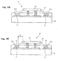
- Figs. 2A and 2B are diagrams for explaining a production of the board of the present invention.
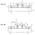
- Figs. 3A and 3B are diagrams for explaining a production of a board according to a related art.
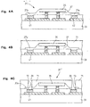
- Figs. 4A to 4C are diagrams for explaining a production of a board of an embodiment according to the present invention in which electronic parts is embedded.
- Fig. 5 is a diagram for illustrating a use of the board of the embodiment according to the present invention in which the electronic parts is embedded.
- Fig. 1 schematically shows a
board 1 according to the present invention. Theboard 1 of the present invention shown in Fig. 1 includes a boardmain body 3 andelectronic parts 5. The boardmain body 3 and theelectronic parts 5 are electrically connected to each other by connecting theirelectrode pads member 17. Theelectrode pad 13a of the boardmain body 3 is formed in an opening part provided in asolder resist layer 9 for covering thewiring 7 of the boardmain body 3 and connected to thewiring 7. On the boardmain body 3, anelectrode pad 13b is also provided for electrically connecting other parts (not shown in the drawing) than theelectronic parts 5 to the board main body. The connectingmember 17 is ordinarily formed by allowing a solder bump arranged on theelectrode pad 15 of theelectronic parts 5 before a connection to re-flow during the connection. A part between thesolder resist layer 9 and theelectronic parts 5 is filled with an under-fill material 19. A part of the under-fillmaterial 19 flows outside a connecting area of theboard 3 and theelectronic parts 5 during heating for hardening the under-fill material to form athin layer 19a in the periphery of theelectronic parts 5. In the thin under-fill material layer 19a in the periphery of theelectronic parts 5, ahole 21 passing through thelayer 19a is provided so as to expose an upper part of theelectrode pad 13b of the boardmain body 3. - As the board
main body 3, a core board or a build-up board generally used for producing a multi-layer wiring board can be employed. Thewiring 7 of the boardmain board 3 is formed with a conductor such as copper. Thepads wiring 7 is made of a conductor formed with, for instance, nickel, and then gold. - A representative example of the
electronic parts 5 mounted on the boardmain body 3 is a semiconductor chip. Further, as theelectronic parts 5, for instance, package parts having the semiconductor chip accommodated in an outer casing may be used. - As the under-fill
material 19, an ordinary under-fill material may be employed that is used for the purpose of preventing a stress resulting from a difference in coefficient of thermal expansion between the boardmain body 3 and theelectronic parts 5 from being concentrated to the connectingmember 17. A representative under-fill material is a thermosetting resin material such as epoxy including filler of an inorganic material (for instance, silica particles). - By referring to Figs. 2A and 2B, a production of the board of the present invention will be described.
- As shown in Fig. 2A,
electronic part 35 is connected to a boardmain body 33 by a flip chip bonding method. A part between the board main body and the electronic parts is filled with an under-fill material 37, the under-fill material is heated and hardened to produce aboard 31 as an intermediate product. In theboard 31 of the intermediate product, in the periphery of theelectronic parts 35, athin layer 37a is located that is formed with the under-fill material flowing outside from an area in which theelectronic parts 35 is mounted during heating and hardening the under-fill material. Under thethin layer 37a of the under-fill material, apad 41 of the boardmain body 33 is located that is used for connecting afterward other parts (not shown in the drawing) than theelectronic parts 35 to the wiring of the board main body. Thepad 41 of the boardmain body 33 is advantageously formed to be rather thick. The reason thereof is described below. Since thelayer 37a formed with the under-fill material flowing to the periphery of theelectronic parts 35 has substantially a uniform thickness, as thepad 41 becomes thicker, the thickness of thelayer 37a located thereon is more reduced, so that a drilling work applied to thelayer 37a afterward is easily performed. - Subsequently, as shown in Fig. 2B, on the
thin layer 37a made of the under-fill material in the periphery of theelectronic parts 35, ahole 39 is formed so as to expose thepad 41 of the boardmain body 33. Thehole 39 can be formed by, for instance, a laser process. It has been known that the laser process is hardly applied to the under-fill material having a filler content more than that of a build-up material (a resin material ordinarily including a filler content as low as about 20 to 30 %). However, for instance, a laser processing machine such as a UV-YAG device (produced by esi corporation) in which a work by the action of heat can be performed is employed so that the drilling work of the under-fill material layer 37a can be carried out. During the laser process, a laser output needs to be controlled so that a harmful influence is not given to theelectronic parts 35 adjacent to thehole 39. Accordingly, a diameter worked by a laser is ordinarily made to be small and the diameter of a hole to be formed is preferably gradually enlarged. For instance, a small hole is firstly opened at a central part of the hole to be formed, a position irradiated with a laser beam is spirally gradually moved outward so that thehole 39 having a desired diameter (for instance, 100 µm) can be opened with a good working accuracy. During the laser process, thepad 41 of thelayer 37a serves as a stopper so that the processing work can be stopped when the depth of the formedhole 39 reaches thepad 41. The hole of thelayer 37a may be opened by a machining work such as a drilling work. However, in the case of the machining work, an influence of vibration to theelectronic parts 35 needs to be considered. Further, since thepad 41 under thelayer 37a does not serve as a stopper more effective than that in the case of the laser process, the thickness of thepad 41 also needs to be considered. - In such a way, a board 31' (Fig. 2B) of the present invention is obtained that has the through
hole 39 provided in the thin under-fill layer 37a in the periphery of theelectronic parts 35 so as to expose the upper part of theelectrode pad 41 of the boardmain body 33. - Now, a production of a board according to a related art will be described below. In this case, as shown in Fig. 3A, means 59 for preventing the outflow of an under-fill material is provided on a solder resist
layer 57 of a boardmain body 53 on whichelectronic parts 55 is mounted by a flip chip bonding method. The under-fill material outflow preventing means 59 shown in this drawing is a dam groove formed in the solder resistlayer 57. Further, on the solder resistlayer 57 outside the dam groove as the under-fill material outflow preventing means, ahole 63 is provided that communicates with apad 61 used for electrically connecting other parts (not shown in the drawing) than theelectronic parts 55 to the board main body. Then, as shown in Fig. 3B, a part between the solder resistlayer 57 and theelectronic parts 55 is filled with an under-fill material 65 and the under-fill material ishardenedbyheatingit. Theunder-fillmaterialflowing out by heating is received by thedam groove 59 to prevent a further outflow. - When the positions of the pads used for connecting other parts than the electronic parts to the board main bodies are compared with each other in the board 31' shown in Fig. 2B according to the present invention and a
board 67 shown in Fig. 3B according to the related art, it is understood that thepad 41 of the board 31' of the present invention is located at a position nearer to the electronic parts than thepad 61 of theboard 67 according to the related art. More specifically, in the board 31' of the present invention, a space D1 (Fig. 2B) between theelectronic parts 35 and thepad 41 can be set to about 2 mm. On the other hand, in theboard 67 according to the related art, as a space D2 (Fig. 3B) between theelectronic parts 55 and thepad 61, at least 5 mm or so is ordinarily necessary. - In the board 31' shown in Fig. 2B according to the present invention, the
electronic parts 35 is mounted on the surface thereof and other parts (not illustrated) can be connected and mounted onto thepad 41 by a wire bonding method. - In the present invention, an embodiment of a type can be realized that electronic parts are embedded in amulti-layer board such as a build-up board. A production of aboard of this embodiment will be described by referring to Figs. 4A to 4C.
- As shown in Fig. 4A, a
board 31 of an intermediate product is prepared. Theboard 31 of the intermediate product is the same as that described with reference to Fig. 2A. Components are respectively designated by the same reference numerals as those of Fig. 2A. Then, a resin material ordinarily used for the build-up board is employed to form an insulatinglayer 71 for coveringelectronic parts 35 as shown in Fig. 4B. Subsequently, a drilling work is applied to the insulatinglayer 71 and athin layer 37a made of an under-fill material in the periphery of theelectronic parts 35 in the same manner as that described by referring to Fig. 2B to formholes layer 71 and thelayer 37a as shown in Fig. 4C. Thus, aboard 31" of the present invention in which theelectronic parts 35 is embedded can be obtained that the throughhole 73 of the insulatinglayer 71 communicates with thehole 39 of thethin layer 37 a made of the under-fill material in the periphery of theelectronic parts 35. - In the board of the present invention in which the insulating layer for embedding the
electronic parts 35 is provided and the throughhole 73 formed in the insulatinglayer 71 communicates with thehole 39 formed in thethin layer 37a of the under-fill material in the periphery of theelectronic parts 35, as shown in Fig. 5, thehole 39 of thelayer 37a of the under-fill material and thehole 73 of the insulatinglayer 71 are filled with aconductor material 75. Awiring 77 is formed that is connected to a part of theconductor material 75 exposed on the surface of the insulatinglayer 71 so as to be used for mounting other parts (not illustrated). As theconductor material 75 with which theholes - In the multi-layer board in which the
electronic parts 35 is embedded as shown in Fig. 5 as an example, to assuredly electrically conduct theelectronic parts 35 to thewiring 77 on another layer or conduct different wiring layers together, a hole passing through the insulating layer needs to be formed. To obtain a high density, it is effective to form such a hole near theelectronic parts 35. However, in the board according to the related art in which the outflow of the under-fill material 37 under theelectronic parts 35 is prevented by the preventing means such as the dam groove, the hole for connecting upper and lower layers is formed outside a layer formed with the flowing out under-fill material. Thus, the board according to the related art cannot adequately meet a demand for a high density. As compared therewith, according to the present invention, the hole for connecting the upper and lower layers can be formed more closely to the electronic parts, so that the board of the present invention can greatly contribute to a promotion of the high density. - In the above description, the board of the structure on which the electronic parts is previously mounted is used for mounting other parts as illustrated in the drawings. However, it is to be understood that the board of the present invention may be mounted on another mounting board and such a use may be included in the embodiment of the present invention.
Claims (6)
- Aboard (1, 31', 31'') with electronic parts mounted by using an under-fill material,
the board comprising:a board main body (3; 33);electronic parts (5; 35) electrically connected to and mounted on the board main body; andan under-fill material (19; 37) with which a part between the board main body and a surface of the electronic parts electrically connected to the board main body is filled, whereina hole (21; 39) passing through a layer (19a; 37a) of the under-fill material that flows outside from a connecting area of the electronic parts and the board main body is provided for electrically connecting other parts to the board main body. - The board according to claim 1, further comprising:an insulating layer in which the electronic parts (5; 35) are embedded, whereina through hole formed in the insulating layer communicates with the hole passing through the layer of the under-fill material (19; 37).
- The board (1, 31' , 31") according to claim 2, wherein
the hole (21; 39) passing through the layer of the under-fill material and the hole formed in the insulating layer are filled with a conductor material. - A method for producing a board (1, 31', 31'') on which electronic parts are mounted by using an under-fill material, the method for producing a board
the method comprising the steps of:connecting the electronic parts (5; 35) to a board main body (3; 33);filling a part between the electronic parts and the board main body with the under-fill material (19; 37); andforming a hole (21; 39) for connecting other parts to the board main body in the board main body, whereinthe hole passes through a layer (19a; 37a) of the under-fill material that flows outside from a connecting area of the electronic parts and the board main body. - The method for producing a board according to claim 4, further comprising the steps of:forming an insulating layer for covering the electronic parts, after the part between the electronic parts (5; 35) and the board main body (3; 33) is filled with the under-fill material, andsuccessively forming holes on the insulating layer and the layer of the under-fill material to form holes for connecting other parts to the board main body.
- The method for producing a board according to any of claims 4 to 5, wherein
the hole for connecting other parts to the board main body (3; 33)is formed by a laser process.
Applications Claiming Priority (1)
| Application Number | Priority Date | Filing Date | Title |
|---|---|---|---|
| JP2005245547A JP2007059767A (en) | 2005-08-26 | 2005-08-26 | Substrate on which electronic components are mounted using underfill material and method for manufacturing the same |
Publications (3)
| Publication Number | Publication Date |
|---|---|
| EP1761116A2 true EP1761116A2 (en) | 2007-03-07 |
| EP1761116A3 EP1761116A3 (en) | 2007-11-07 |
| EP1761116B1 EP1761116B1 (en) | 2009-05-20 |
Family
ID=37532991
Family Applications (1)
| Application Number | Title | Priority Date | Filing Date |
|---|---|---|---|
| EP06017440A Ceased EP1761116B1 (en) | 2005-08-26 | 2006-08-22 | Circuit board having electronic parts mounted thereon by using under-fill material and method for producing the same |
Country Status (7)
| Country | Link |
|---|---|
| US (1) | US7663253B2 (en) |
| EP (1) | EP1761116B1 (en) |
| JP (1) | JP2007059767A (en) |
| KR (1) | KR20070024366A (en) |
| CN (1) | CN100521178C (en) |
| DE (1) | DE602006006885D1 (en) |
| TW (1) | TW200713476A (en) |
Families Citing this family (12)
| Publication number | Priority date | Publication date | Assignee | Title |
|---|---|---|---|---|
| TWI315658B (en) * | 2007-03-02 | 2009-10-01 | Phoenix Prec Technology Corp | Warp-proof circuit board structure |
| JP5003260B2 (en) * | 2007-04-13 | 2012-08-15 | 日本電気株式会社 | Semiconductor device and manufacturing method thereof |
| AU2010210385A1 (en) * | 2009-02-06 | 2011-08-18 | Velomedix, Inc. | Method and apparatus for inducing therapeutic hypothermia |
| JP2011060892A (en) * | 2009-09-08 | 2011-03-24 | Renesas Electronics Corp | Electronic device and method for manufacturing the same |
| TWI514530B (en) * | 2013-08-28 | 2015-12-21 | 威盛電子股份有限公司 | Circuit substrate, semiconductor package structure and circuit substrate process |
| KR20160022603A (en) | 2014-08-20 | 2016-03-02 | 삼성전기주식회사 | Flip chip package and method for manufacturing thereof |
| JP6453625B2 (en) * | 2014-11-27 | 2019-01-16 | 新光電気工業株式会社 | WIRING BOARD, MANUFACTURING METHOD THEREOF, AND ELECTRONIC COMPONENT DEVICE |
| CN111052367A (en) * | 2017-01-31 | 2020-04-21 | 天工方案公司 | Control of underfill for dual-sided ball grid array packages |
| US10460957B2 (en) * | 2017-01-31 | 2019-10-29 | Skyworks Solutions, Inc. | Control of under-fill using an encapsulant for a dual-sided ball grid array package |
| KR102853612B1 (en) * | 2020-07-15 | 2025-09-03 | 삼성전자주식회사 | Semiconductor package and method of fabricating the same |
| US12237300B2 (en) | 2020-12-07 | 2025-02-25 | Intel Corporation | Through-substrate void filling for an integrated circuit assembly |
| US12341121B2 (en) | 2020-12-07 | 2025-06-24 | Intel Corporation | Through-substrate underfill formation for an integrated circuit assembly |
Citations (1)
| Publication number | Priority date | Publication date | Assignee | Title |
|---|---|---|---|---|
| JP2000164610A (en) | 1998-11-30 | 2000-06-16 | Ngk Spark Plug Co Ltd | Semiconductor device and manufacturing method thereof |
Family Cites Families (8)
| Publication number | Priority date | Publication date | Assignee | Title |
|---|---|---|---|---|
| EP0604823A1 (en) * | 1992-12-29 | 1994-07-06 | International Business Machines Corporation | Triazine polymer and use thereof |
| JP3833859B2 (en) * | 1999-10-14 | 2006-10-18 | ローム株式会社 | Semiconductor device and manufacturing method thereof |
| JP3670917B2 (en) * | 1999-12-16 | 2005-07-13 | 新光電気工業株式会社 | Semiconductor device and manufacturing method thereof |
| JP3598060B2 (en) * | 1999-12-20 | 2004-12-08 | 松下電器産業株式会社 | CIRCUIT COMPONENT MODULE, MANUFACTURING METHOD THEREOF, AND RADIO DEVICE |
| US20030113952A1 (en) | 2001-12-19 | 2003-06-19 | Mahesh Sambasivam | Underfill materials dispensed in a flip chip package by way of a through hole |
| JP4137659B2 (en) * | 2003-02-13 | 2008-08-20 | 新光電気工業株式会社 | Electronic component mounting structure and manufacturing method thereof |
| WO2005076352A1 (en) * | 2004-02-05 | 2005-08-18 | Renesas Technology Corp. | Semiconductor device and method for manufacturing semiconductor device |
| JP2006041239A (en) | 2004-07-28 | 2006-02-09 | Toshiba Corp | Wiring board and magnetic disk device |
-
2005
- 2005-08-26 JP JP2005245547A patent/JP2007059767A/en active Pending
-
2006
- 2006-08-08 US US11/463,169 patent/US7663253B2/en not_active Expired - Fee Related
- 2006-08-14 TW TW095129761A patent/TW200713476A/en unknown
- 2006-08-18 KR KR1020060078029A patent/KR20070024366A/en not_active Withdrawn
- 2006-08-22 DE DE602006006885T patent/DE602006006885D1/en active Active
- 2006-08-22 EP EP06017440A patent/EP1761116B1/en not_active Ceased
- 2006-08-25 CN CNB2006101099791A patent/CN100521178C/en not_active Expired - Fee Related
Patent Citations (1)
| Publication number | Priority date | Publication date | Assignee | Title |
|---|---|---|---|---|
| JP2000164610A (en) | 1998-11-30 | 2000-06-16 | Ngk Spark Plug Co Ltd | Semiconductor device and manufacturing method thereof |
Also Published As
| Publication number | Publication date |
|---|---|
| JP2007059767A (en) | 2007-03-08 |
| EP1761116A3 (en) | 2007-11-07 |
| US20070045867A1 (en) | 2007-03-01 |
| TW200713476A (en) | 2007-04-01 |
| CN100521178C (en) | 2009-07-29 |
| CN1921097A (en) | 2007-02-28 |
| DE602006006885D1 (en) | 2009-07-02 |
| US7663253B2 (en) | 2010-02-16 |
| EP1761116B1 (en) | 2009-05-20 |
| KR20070024366A (en) | 2007-03-02 |
Similar Documents
| Publication | Publication Date | Title |
|---|---|---|
| JP5018826B2 (en) | Electronic device and manufacturing method thereof | |
| CN100576977C (en) | Bare chip embedded PCB and manufacturing method thereof | |
| JP3277997B2 (en) | Ball grid array package and manufacturing method thereof | |
| EP1761116B1 (en) | Circuit board having electronic parts mounted thereon by using under-fill material and method for producing the same | |
| US9288910B2 (en) | Substrate with built-in electronic component and method for manufacturing substrate with built-in electronic component | |
| KR20080088403A (en) | Manufacturing Method of Wiring Board, Manufacturing Method of Semiconductor Device and Wiring Board | |
| CN101594754A (en) | Method for producing printed wiring board and conductive adhesive | |
| WO2008047918A1 (en) | Electronic device package structure and package manufacturing method | |
| US20110266671A1 (en) | Substrate for a semiconductor package and manufacturing method thereof | |
| CN111834093A (en) | Substrate with built-in inductor | |
| JP2016149517A (en) | Wiring board and manufacturing method thereof | |
| US20030141600A1 (en) | Apparatus and method of manufacturing printed circuit boards | |
| KR20150065029A (en) | Printed circuit board, manufacturing method thereof and semiconductor package | |
| US20040262033A1 (en) | Printed circuit board and method for fabricating the same | |
| EP1043921A1 (en) | Multilayer printed wiring board and method for manufacturing the same | |
| JP2013211426A (en) | Component built-in wiring board and manufacturing method of the same | |
| JP4282161B2 (en) | Multilayer printed wiring board and method for manufacturing multilayer printed wiring board | |
| JP5000105B2 (en) | Semiconductor device | |
| TWI292948B (en) | ||
| JP5311656B2 (en) | Wiring board | |
| JP2008181920A (en) | Electronic component-embedded substrate, electronic device using the same, and manufacturing method thereof | |
| KR102107035B1 (en) | Printed circuit board and method of manufacturing the same | |
| KR100974244B1 (en) | Method of manufacturing semiconductor package substrate and semiconductor package substrate | |
| KR100887685B1 (en) | Manufacturing Method of Printed Circuit Board with Electronic Device | |
| KR20110122044A (en) | Semiconductor package substrate and manufacturing method thereof |
Legal Events
| Date | Code | Title | Description |
|---|---|---|---|
| PUAI | Public reference made under article 153(3) epc to a published international application that has entered the european phase |
Free format text: ORIGINAL CODE: 0009012 |
|
| AK | Designated contracting states |
Kind code of ref document: A2 Designated state(s): AT BE BG CH CY CZ DE DK EE ES FI FR GB GR HU IE IS IT LI LT LU LV MC NL PL PT RO SE SI SK TR |
|
| AX | Request for extension of the european patent |
Extension state: AL BA HR MK YU |
|
| PUAL | Search report despatched |
Free format text: ORIGINAL CODE: 0009013 |
|
| AK | Designated contracting states |
Kind code of ref document: A3 Designated state(s): AT BE BG CH CY CZ DE DK EE ES FI FR GB GR HU IE IS IT LI LT LU LV MC NL PL PT RO SE SI SK TR |
|
| AX | Request for extension of the european patent |
Extension state: AL BA HR MK YU |
|
| RIC1 | Information provided on ipc code assigned before grant |
Ipc: H05K 1/18 20060101ALI20071001BHEP Ipc: H05K 3/30 20060101ALI20071001BHEP Ipc: H01L 21/56 20060101AFI20071001BHEP Ipc: H01L 23/31 20060101ALI20071001BHEP |
|
| 17P | Request for examination filed |
Effective date: 20080109 |
|
| AKX | Designation fees paid |
Designated state(s): DE |
|
| GRAP | Despatch of communication of intention to grant a patent |
Free format text: ORIGINAL CODE: EPIDOSNIGR1 |
|
| RIN1 | Information on inventor provided before grant (corrected) |
Inventor name: MACHIDA, YOSHIHIROC/O SHINKO ELECTRIC INDUSTRIES C |
|
| GRAS | Grant fee paid |
Free format text: ORIGINAL CODE: EPIDOSNIGR3 |
|
| GRAA | (expected) grant |
Free format text: ORIGINAL CODE: 0009210 |
|
| AK | Designated contracting states |
Kind code of ref document: B1 Designated state(s): DE |
|
| REF | Corresponds to: |
Ref document number: 602006006885 Country of ref document: DE Date of ref document: 20090702 Kind code of ref document: P |
|
| PLBE | No opposition filed within time limit |
Free format text: ORIGINAL CODE: 0009261 |
|
| STAA | Information on the status of an ep patent application or granted ep patent |
Free format text: STATUS: NO OPPOSITION FILED WITHIN TIME LIMIT |
|
| 26N | No opposition filed |
Effective date: 20100223 |
|
| PGFP | Annual fee paid to national office [announced via postgrant information from national office to epo] |
Ref country code: DE Payment date: 20200812 Year of fee payment: 15 |
|
| REG | Reference to a national code |
Ref country code: DE Ref legal event code: R119 Ref document number: 602006006885 Country of ref document: DE |
|
| PG25 | Lapsed in a contracting state [announced via postgrant information from national office to epo] |
Ref country code: DE Free format text: LAPSE BECAUSE OF NON-PAYMENT OF DUE FEES Effective date: 20220301 |