EP1760775A1 - Semiconductor device with through electrode and method of manufacturing the same - Google Patents
Semiconductor device with through electrode and method of manufacturing the same Download PDFInfo
- Publication number
- EP1760775A1 EP1760775A1 EP06018011A EP06018011A EP1760775A1 EP 1760775 A1 EP1760775 A1 EP 1760775A1 EP 06018011 A EP06018011 A EP 06018011A EP 06018011 A EP06018011 A EP 06018011A EP 1760775 A1 EP1760775 A1 EP 1760775A1
- Authority
- EP
- European Patent Office
- Prior art keywords
- layer
- forming
- electrode
- semiconductor element
- surface side
- Prior art date
- Legal status (The legal status is an assumption and is not a legal conclusion. Google has not performed a legal analysis and makes no representation as to the accuracy of the status listed.)
- Granted
Links
Images




Classifications
-
- H—ELECTRICITY
- H10—SEMICONDUCTOR DEVICES; ELECTRIC SOLID-STATE DEVICES NOT OTHERWISE PROVIDED FOR
- H10W—GENERIC PACKAGES, INTERCONNECTIONS, CONNECTORS OR OTHER CONSTRUCTIONAL DETAILS OF DEVICES COVERED BY CLASS H10
- H10W20/00—Interconnections in chips, wafers or substrates
- H10W20/01—Manufacture or treatment
- H10W20/021—Manufacture or treatment of interconnections within wafers or substrates
- H10W20/023—Manufacture or treatment of interconnections within wafers or substrates the interconnections being through-semiconductor vias
-
- H—ELECTRICITY
- H10—SEMICONDUCTOR DEVICES; ELECTRIC SOLID-STATE DEVICES NOT OTHERWISE PROVIDED FOR
- H10W—GENERIC PACKAGES, INTERCONNECTIONS, CONNECTORS OR OTHER CONSTRUCTIONAL DETAILS OF DEVICES COVERED BY CLASS H10
- H10W20/00—Interconnections in chips, wafers or substrates
- H10W20/01—Manufacture or treatment
- H10W20/021—Manufacture or treatment of interconnections within wafers or substrates
- H10W20/023—Manufacture or treatment of interconnections within wafers or substrates the interconnections being through-semiconductor vias
- H10W20/0238—Manufacture or treatment of interconnections within wafers or substrates the interconnections being through-semiconductor vias comprising etching via holes through pads or through electrodes
-
- H—ELECTRICITY
- H10—SEMICONDUCTOR DEVICES; ELECTRIC SOLID-STATE DEVICES NOT OTHERWISE PROVIDED FOR
- H10W—GENERIC PACKAGES, INTERCONNECTIONS, CONNECTORS OR OTHER CONSTRUCTIONAL DETAILS OF DEVICES COVERED BY CLASS H10
- H10W20/00—Interconnections in chips, wafers or substrates
- H10W20/01—Manufacture or treatment
- H10W20/021—Manufacture or treatment of interconnections within wafers or substrates
- H10W20/023—Manufacture or treatment of interconnections within wafers or substrates the interconnections being through-semiconductor vias
- H10W20/0261—Manufacture or treatment of interconnections within wafers or substrates the interconnections being through-semiconductor vias characterised by the filling method or the material of the conductive fill
-
- H—ELECTRICITY
- H10—SEMICONDUCTOR DEVICES; ELECTRIC SOLID-STATE DEVICES NOT OTHERWISE PROVIDED FOR
- H10W—GENERIC PACKAGES, INTERCONNECTIONS, CONNECTORS OR OTHER CONSTRUCTIONAL DETAILS OF DEVICES COVERED BY CLASS H10
- H10W20/00—Interconnections in chips, wafers or substrates
- H10W20/20—Interconnections within wafers or substrates, e.g. through-silicon vias [TSV]
-
- H—ELECTRICITY
- H10—SEMICONDUCTOR DEVICES; ELECTRIC SOLID-STATE DEVICES NOT OTHERWISE PROVIDED FOR
- H10P—GENERIC PROCESSES OR APPARATUS FOR THE MANUFACTURE OR TREATMENT OF DEVICES COVERED BY CLASS H10
- H10P14/00—Formation of materials, e.g. in the shape of layers or pillars
- H10P14/40—Formation of materials, e.g. in the shape of layers or pillars of conductive or resistive materials
- H10P14/46—Formation of materials, e.g. in the shape of layers or pillars of conductive or resistive materials using a liquid
- H10P14/47—Electrolytic deposition, i.e. electroplating; Electroless plating
-
- H—ELECTRICITY
- H10—SEMICONDUCTOR DEVICES; ELECTRIC SOLID-STATE DEVICES NOT OTHERWISE PROVIDED FOR
- H10W—GENERIC PACKAGES, INTERCONNECTIONS, CONNECTORS OR OTHER CONSTRUCTIONAL DETAILS OF DEVICES COVERED BY CLASS H10
- H10W70/00—Package substrates; Interposers; Redistribution layers [RDL]
- H10W70/60—Insulating or insulated package substrates; Interposers; Redistribution layers
- H10W70/62—Insulating or insulated package substrates; Interposers; Redistribution layers characterised by their interconnections
- H10W70/65—Shapes or dispositions of interconnections
-
- H—ELECTRICITY
- H10—SEMICONDUCTOR DEVICES; ELECTRIC SOLID-STATE DEVICES NOT OTHERWISE PROVIDED FOR
- H10W—GENERIC PACKAGES, INTERCONNECTIONS, CONNECTORS OR OTHER CONSTRUCTIONAL DETAILS OF DEVICES COVERED BY CLASS H10
- H10W72/00—Interconnections or connectors in packages
- H10W72/20—Bump connectors, e.g. solder bumps or copper pillars; Dummy bumps; Thermal bumps
- H10W72/241—Dispositions, e.g. layouts
- H10W72/244—Dispositions, e.g. layouts relative to underlying supporting features, e.g. bond pads, RDLs or vias
-
- H—ELECTRICITY
- H10—SEMICONDUCTOR DEVICES; ELECTRIC SOLID-STATE DEVICES NOT OTHERWISE PROVIDED FOR
- H10W—GENERIC PACKAGES, INTERCONNECTIONS, CONNECTORS OR OTHER CONSTRUCTIONAL DETAILS OF DEVICES COVERED BY CLASS H10
- H10W72/00—Interconnections or connectors in packages
- H10W72/50—Bond wires
- H10W72/551—Materials of bond wires
- H10W72/552—Materials of bond wires comprising metals or metalloids, e.g. silver
- H10W72/5522—Materials of bond wires comprising metals or metalloids, e.g. silver comprising gold [Au]
-
- H—ELECTRICITY
- H10—SEMICONDUCTOR DEVICES; ELECTRIC SOLID-STATE DEVICES NOT OTHERWISE PROVIDED FOR
- H10W—GENERIC PACKAGES, INTERCONNECTIONS, CONNECTORS OR OTHER CONSTRUCTIONAL DETAILS OF DEVICES COVERED BY CLASS H10
- H10W72/00—Interconnections or connectors in packages
- H10W72/851—Dispositions of multiple connectors or interconnections
- H10W72/874—On different surfaces
- H10W72/884—Die-attach connectors and bond wires
-
- H—ELECTRICITY
- H10—SEMICONDUCTOR DEVICES; ELECTRIC SOLID-STATE DEVICES NOT OTHERWISE PROVIDED FOR
- H10W—GENERIC PACKAGES, INTERCONNECTIONS, CONNECTORS OR OTHER CONSTRUCTIONAL DETAILS OF DEVICES COVERED BY CLASS H10
- H10W72/00—Interconnections or connectors in packages
- H10W72/90—Bond pads, in general
- H10W72/921—Structures or relative sizes of bond pads
- H10W72/922—Bond pads being integral with underlying chip-level interconnections
-
- H—ELECTRICITY
- H10—SEMICONDUCTOR DEVICES; ELECTRIC SOLID-STATE DEVICES NOT OTHERWISE PROVIDED FOR
- H10W—GENERIC PACKAGES, INTERCONNECTIONS, CONNECTORS OR OTHER CONSTRUCTIONAL DETAILS OF DEVICES COVERED BY CLASS H10
- H10W90/00—Package configurations
- H10W90/701—Package configurations characterised by the relative positions of pads or connectors relative to package parts
- H10W90/751—Package configurations characterised by the relative positions of pads or connectors relative to package parts of bond wires
- H10W90/754—Package configurations characterised by the relative positions of pads or connectors relative to package parts of bond wires between a chip and a stacked insulating package substrate, interposer or RDL
Definitions
- the present disclosure relates to connections of semiconductor devices. More particularly, the present disclosure relates to a semiconductor device constructed to form electrodes connected to electrode pads of a semiconductor element that has a device forming layer and the electrode pads on its one surface side, and a method of manufacturing the same.
- the semiconductor device having such a structure that the electrodes of the semiconductor element as typified by the optoelectronic element such as the light receiving element, the light emitting element, or the like, in which the device forming layer is formed on the substrate, are connected to the wiring patterns formed on the substrate, there is the semiconductor device constructed as shown in FIG.7.
- a semiconductor element 14 is adhered onto a wiring substrate 12 by an adhesive 16 and a device forming layer 18 and Al electrode pads 20 are formed on an upper surface of the semiconductor element 14.
- a plurality of Al electrode pads 20 provided around the device forming layer 18 are connected to wiring patterns 24 on the wiring substrate 12 via Au wires 22 stretched by the wire bonding.
- a passivating layer (protection film) 26 is laminated on a surface of the device forming layer 18 (device surface).
- the method of flip-flop connecting a plurality of Al electrode pads 20 to the wiring patterns 24 via the solder bumps may be considered.
- a light is blocked by the wiring substrate 12 because the device forming layer 18 opposes to the wiring substrate 12. Therefore, this method cannot be employed in the optoelectronic element whose device forming layer 18 receives a light or emits a light.
- an inner peripheral shape of the through hole is formed as a taper shape (an opening on the upper surface side has a large diameter and an opening on the lower surface side has a small diameter). Therefore, the through holes that are opened largely must be formed on the upper surface side of the semiconductor element 14, on which the device forming layer 18 is formed, and the through holes must be formed in positions that are away correspondingly from the device forming layer 18. As a result, such a problem exists that it is hindered that a miniaturization of the semiconductor device should be achieved.
- the method of employing the dry etching is considered. In this case, such a problem arises that the device forming layer of the semiconductor element is damaged depending on the plasma atmosphere in the dry etching.
- Embodiments of the present invention provide a semiconductor device capable of achieving a size reduction of the device and forming through holes and through electrodes in a state that a device forming layer is protected, and a method of manufacturing the same.
- a method of manufacturing a semiconductor device having a through electrode that connects an electrode pad of a semiconductor element, which has a device forming layer and the electrode pad on one surface side, and the other surface side of the semiconductor element which includes a first step of forming a first resist layer on surfaces of the electrode pad and the device forming layer on one surface side of the semiconductor element; a second step of forming an opening in the electrode pad by an etching; a third step of forming a through hole, one end of which is communicated with the opening and another end of which is opened on the other surface side of the semiconductor element, in the semiconductor element by the etching; and a fourth step of forming the through electrode in the through hole.
- the second step contains a step of forming a second resist layer on an inner periphery of the opening in the electrode pad.
- a third aspect of one or more embodiments of the invention provides the method of manufacturing the semiconductor device, which further includes a fifth step of pasting a protection film on a surface of the first resist layer or the second resist layer.
- a fourth aspect of one or more embodiments of the invention provides the method of manufacturing the semiconductor device, which further includes a sixth step of forming an insulating layer from the other surface side of the semiconductor element to spread the insulating layer on an inner peripheral of the through hole, which extends to one surface side of the semiconductor element, and a lower surface of the protection film.
- a fifth aspect of one or more embodiments of the invention provides the method of manufacturing the semiconductor device, which further includes a seventh step of exposing one side of the through hole by releasing the protection film.
- a sixth aspect of one or more embodiments of the invention provides the method of manufacturing the semiconductor device, which further includes an eighth step of forming a power feeding layer on other surface side of the semiconductor element and forming the through electrode in the through hole by plating.
- a seventh aspect of one or more embodiments of the invention provides a semiconductor device comprising: an electrode pad formed on one surface side of a semiconductor element, on which a device forming layer is formed, via an insulating layer; a through hole formed by an etching to pass through the electrode pad and the semiconductor element in a state that a resist is coated on the one surface side of the semiconductor element; an insulating layer formed on an inner periphery of the through hole to project from the through hole to one surface side of the semiconductor element; a through electrode formed in the insulating layer, the through electrode connecting the electrode pad and the other surface side of the semiconductor element; and a conductive layer for connecting the electrode pad formed on an outer side of the insulating layer and an end portion of the through hole.
- the device forming layer is an optically functioning element to receive a light or emit the light.
- the device forming layer is an image sensor to sense a light and output an image signal.
- the first resist layer is formed on the surfaces of the electrode pads and the device forming layer on one surface side of the semiconductor element on which the device forming layer and the electrode pads are formed. Accordingly, the device forming layer is protected by the first resist layer when the opening is formed in the electrode pad by the etching, so that the through holes can be formed in such a condition that the device forming layer is not damaged by the plasma. Therefore, a miniaturization can be accomplished by forming the fine through holes in vicinity of the device forming layer, and also the through holes can be formed from the side on which the device forming layer is mounted. As a result, an alignment needed when the through holes are processed can be executed easily.
- the second resist layer is formed on the inner periphery of the opening of the electrode pad. Therefore, the inner peripheral surface of the electrode pad can be protected when the through hole communicated with the opening in the electrode pad is formed by the dry etching.
- the protection film is pasted on the surface of the first resist layer or the second resist layer to close the through holes from one side of the substrate. Therefore, the insulating layer can be formed on the overall inner surfaces of the through holes from the other side of the substrate, and also one side of the through hole can be opened by a simple operation, i.e., by peeling off the protection film.
- the through electrodes can be formed in a state that the device forming layer composed of the optically functioning element is formed on the upper surface side of the substrate, the through electrodes can be fitted into the wiring substrate by the flip-chip connection via the rewiring on the lower surface side of the semiconductor element, and the through electrodes can be constructed not to disturb a light reception or a light emission of the device forming layer composed of the optically functioning element.
- Embodiments according to the invention are also directed to methods by which the described apparatus is manufactured. It includes method steps for carrying out every function of the apparatus or manufacturing every part of the apparatus.
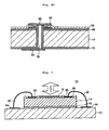
- FIG.1 is a longitudinal sectional view showing an embodiment of a semiconductor device according to the present invention.
- a semiconductor device 50 is constructed by forming through electrodes, each connects the Al electrode pad 20 and a rewiring pattern 52, in the semiconductor element 14 (including the device forming layer 18 formed of the optically functioning element, the Al electrode pads 20, the passivating layer 26, and an insulating layer 60).
- the light receiving element for receiving a light, the light emitting element for emitting a light, the image sensor for sensing a light to output an image signal, or the like, for example, is cited as the device forming layer 18.
- a plurality of Al electrode pads 20 connected electrically to the device forming layer 18 are provided around the device forming layer 18, and the rewiring patterns 52 are provided on a lower surface of the semiconductor element 14.
- Through holes 54 passing through the semiconductor element 14 are provided between the Al electrode pads 20 and the rewiring patterns 52 by the dry etching.
- Through electrodes 56 are formed in insides of the through holes 54 by the Cu plating.
- the rewiring patterns 52 provided on the lower surface of the semiconductor element 14 are connected to the wiring patterns 24 on the wiring substrate 12 via solder bumps 58.
- the semiconductor device 50 is constructed to connect the Al electrode pads 20 and the rewiring patterns 52 via the through electrodes 56 and flip-chip connect the rewiring patterns 52 of the semiconductor element 14 and the wiring patterns 24 on the wiring substrate 12 via the solder bumps 58. Therefore, a considerable size reduction can be accomplished rather than the configuration using the wire bonding (see FIG.7) in the related art.
- the semiconductor device 50 is constructed not to disturb the light reception or the light emission of the device forming layer 18.
- the method of manufacturing the semiconductor device 50 for example, there are the manufacturing methods (a) to (c) described in the following.
- the manufacturing method in (a) is employed.
- the through electrodes 56 can be formed collectively in the silicon substrate having a large number of semiconductor elements 14, and therefore a mass productivity can be enhanced much more.
- steps of manufacturing the through electrodes 56 of the semiconductor device 50 will be explained in detail hereunder.
- the steps of manufacturing the through electrodes 56 are roughly classified into (1) step of forming the opening, (2) step of forming the insulating layer, (3) step of forming the through electrode, (4) step of ensuring an electrical continuity between the electrode pad and the through electrode, and (5) step of rewiring and removing the resist.
- FIG.2A to FIG.6C for convenience of explanation, the Al electrode pads 20, which are connected to the device forming layer 18 and the through electrodes 56, and their neighboring areas are depicted in an enlarged fashion, and the device forming layer 18 is omitted from the illustration.
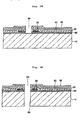
- FIG.2A to FIG.2F are views explaining steps (#1 to #6) of forming an opening in a method of manufacturing a semiconductor device according to the present invention.
- a flat plate silicon material silicon substrate used to form the semiconductor elements 14 is prepared.
- the insulating layer (SiO 2 ) 60 is formed on the upper surface (front surface) of the silicon substrate (for convenience, illustrated as the semiconductor elements 14 in FIG.2 to FIG.6), and then the device forming layer 18 is formed on the upper surface of the insulating layer 60.
- the Al electrode pad 20 is formed around the device forming layer 18 by the thin film forming method such as the vapor deposition, or the like. Also, the passivating layer 26 such as SiN, polyimide, or the like is stacked on the surface of the insulating layer 60 and the upper surface of the Al electrode pad 20 except its center portion.
- the passivating layer 26 such as SiN, polyimide, or the like is stacked on the surface of the insulating layer 60 and the upper surface of the Al electrode pad 20 except its center portion.
- a first resist layer 62 is formed by coating the photoresist on a surface of the passivating layer 26.
- the photoresist is the positive resist
- the photoresist coated on a center portion of upper surface of the Al electrode pad 20 is fused by irradiating a light onto the center portions of the upper surfaces of the Al electrode pad 20.
- an opening 64 is formed to oppose to the center portions of the upper surface of the Al electrode pad 20.
- the photoresist is the negative resist
- the photoresist coated on the center portion of the upper surfaces of the Al electrode pad 20 is fused by irradiating a light onto peripheral portions except the center portion of the upper surface of the Al electrode pad 20.
- the opening 64 is formed. Also, in this step, since the opening 64 is formed in the first resist layer 62 by irradiating a light from the top side of the semiconductor element 14, an alignment on the lower surface (back surface) of the semiconductor element 14 is not needed.
- the opening 64 is provided in the center portion of the Al electrode pad 20 by the dry etching.
- the dry etching such as the reactive ion etching
- positive ions in the plasma are shot into the center portions of the upper surfaces of the Al electrode pads 20, which are not covered with the first resist layer 62, and thus the center portion of the Al electrode pad 20 is removed from the top in the vertical direction.
- the A1 electrode pad 20 has a hollow shape having the opening 64 in its center portion. Also, since the device forming layer 18 is covered with the first resist layer 62 during the dry etching of the opening 64, there is no possibility that the device forming layer 18 is damaged.
- a second resist layer 66 is formed by coating the photoresist on the surface of the first resist layer 62 and an inner peripheral surface of the opening 64 and patterning the photoresist.
- the second resist layer 66 aims at protecting the inner peripheral surface of the opening 64. Therefore, a thickness of the second resist layer 66 may be set thinner than that of the first resist layer 62. Also, if the inner peripheral surface of the opening 64 is not damaged by the plasma when the through hole 54 is formed in the semiconductor element 14 by the dry etching, the second resist layer 66 can be omitted.
- a portion of the semiconductor element 14, which is communicated with the opening 64, is removed from the top side by the dry etching, and thus the through hole 54 is passed through up to the bottom surface side of the semiconductor element 14.
- the inner peripheral surface of the Al electrode pad 20 is protected from the plasma by the second resist layer 66, and also the device forming layer 18 is protected by the first resist layer 62.
- the through hole 54 can be provided by the dry etching from the top side of the semiconductor element 14 on which the device forming layer 18 is formed. Therefore, the fine through hole 54 having a high aspect ratio can be formed and also it can be prevented by the first resist layer 62 and the second resist layer 66 that the device forming layer 18 and the inner peripheral surface of the Al electrode pad 20 are damaged by the plasma.
- the opening 64 and the through hole 54 can be processed from the upper surface side, an alignment to be applied from the back surface side can be omitted and also the opening forming steps can be easily executed.
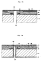
- FIG.3A to FIG.3C are views explaining steps (#1 to #3) of forming an insulating layer in a method of manufacturing a semiconductor device according to the present invention.
- a protection film 70 made of a resin is pasted on an upper surface of the second resist layer 66. This protection film 70 protects the device forming layer 18 and also closes the opening 64 communicated with the through hole 54 from the upper surface side.
- an insulating layer 72 made of SiO 2 , SiN, organic insulating film such as polymide or the like is formed from the lower surface side of the semiconductor element 14 by the thin film forming method such as the plasma CVD (Chemical Vapor Deposition), PVD (Physical Vapor Deposition) or the like. Also, the insulating layer 72 is coated and formed on the lower surface side of the semiconductor element 14, the inner peripheral surface of the through hole 54, and the inner peripheral surface of the opening 64. Also, since the upper surface side of the opening 64 is blocked by the protection film 70, the insulating layer 72 is also formed on a lower surface of the protection film 70 that contacts the openings 64.
- the thin film forming method such as the plasma CVD (Chemical Vapor Deposition), PVD (Physical Vapor Deposition) or the like. Also, the insulating layer 72 is coated and formed on the lower surface side of the semiconductor element 14, the inner peripheral surface of the through hole 54, and the inner peripheral surface of the opening 64. Also, since the upper
- the protection film 70 is released. Since this protection film 70 can be released while a portion of the insulating layer 72 to close the opening 64 is being stuck to its lower surface, the cylindrical insulating layer 72 for covering the inner peripheral surfaces of the through hole 54 and the opening 64 is formed to pass through from the upper surface side to the lower surface side. Since all steps applied from the dry etching of the through hole 54 and the opening 64 to the formation of the insulating layer 72 are the dry step, the inner peripheral surfaces of the through hole 54 and the opening 64 are maintained in a clean condition. Therefore, the step of cleaning the through hole 54 and the opening 64 can be omitted.
- FIG.4A to FIG. 4C are views explaining steps (#1 to #3) of forming a through electrode in a method of manufacturing a semiconductor device according to the present invention.
- a power feeding layer 80 is formed by pasting a conductive material on a lower surface of the insulating layer 72. Therefore, the lower surface side of the through hole 54 is closed by the power feeding layer 80.
- the through electrode 56 is formed in the through hole 54 by the plating.
- a metal Cu, Au, or the like
- the through electrode 56 is formed in the through hole 54 and the opening 64. In this case, an upper end portion of the through electrode 56 is projected upward from the opening 64.
- the upper surface side of a resultant structure is polished and planarized by the CMP (Chemical Mechanical Polishing).
- CMP Chemical Mechanical Polishing
- the through electrode 56 can be filled in the inside of the cylindrical insulating layer 72, which covers the inner peripheral surfaces of the through hole 54 and the opening 64, while using the power feeding layer 80 as the base.
- the second resist layer 66 may be left if the top end portion of the through electrode 56 can be planarized.
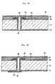
- FIG.5A to FIG.5D are views explaining steps (#1 to #4) of ensuring an electrical continuity between an electrode pad and a through electrode in a method of manufacturing a semiconductor device according to the present invention.
- a third resist layer 82 is formed by coating the photoresist on the planarized upper surface.
- an opening 84 is formed by removing a portion of the third resist layer 82, which covers an area located over the Al electrode pad 20.
- the third resist layer 82 is coated thicker than the first resist layer 62 and the second resist layer 66.
- the first resist layer 62 and the second resist layer 66 left around the top end portion of the through electrode 56 are removed by applying the ashing from the upper surface side. Accordingly, the inner periphery of the Al electrode pad 20 and the top end portion of the through electrode 56 covered with the insulating layer 72 are exposed, so that a recess portion 86 from which the top portion of the through electrode 56 is projected in a position that is lower than the third resist layer 82 is exposed.
- a surface layer portion of the third resist layer 82 is removed by the ashing.
- the third resist layer 82 is coated thick, the device forming layer 18 is protected by the third resist layer 82 even when the first resist layer 62 and the second resist layer 66 left around the top end portion of the through electrode 56 are removed by the ashing.
- a metal layer (conductive member) 88 is formed from the top side by the thin film forming method such as the sputter, or the like.
- the metal layer 88 is a thin film made of a conductive material such as copper, or the like, and is deposited on the inside of the recess portion 86 that is formed like an annular recess by the ashing in a position that is lower than the third resist layer 82. Therefore, the inner periphery of the Al electrode pad 20 and the top portion of the through electrode 56 are connected conductively via the metal layer 88.
- the metal layer 88 stacked on the third resist layer 82 is removed by the etching, the CMP, or the like except the portion that connects conductively the Al electrode pad 20 and the through electrode 56, and thus an upper surface is planarized.
- the device forming layer 18 is still protected by the first resist layer 62 even after the upper surface is planarized by removing the unnecessary portion of the metal layer 88 in this step.
- the metal layer 88 functions as a conductive layer that connects the Al electrode pad 20 formed on the outside of the insulating layer 72 and the end portion of the through electrode 56 formed in the inside of the insulating layer 72. Also, the metal layer 88 is provided in an unreleasable condition because its adhering area is increased by a level difference between the outer periphery of the cylindrical insulating layer 72 projected to the upper surface side and the Al electrode pad 20 and a level difference between the passivating layer 26 and the Al electrode pad 20.
- FIG.6A to FIG.6C are views explaining steps (#1 to #3) of rewiring and removing a resist in a method of manufacturing a semiconductor device according to the present invention.
- the insulating layer 72 is exposed by removing the power feeding layer 80 formed on the lower surface side (back surface side) of the semiconductor element 14 by means of the etching.
- the rewiring pattern 52 is formed by forming a metal layer such as Cu, or the like on the lower surface side (back surface side) of the semiconductor element 14 by the sputter method and etching the metal layer. Also, the rewiring pattern may be formed on the upper surface side (front surface side) of the semiconductor element 14, as the case may be.
- the first resist layer 62 and the third resist layer 82 left on the upper surface side (front surface side) of the semiconductor element 14 are removed.
- the first resist layer 62 for protecting the device forming layer 18 is formed at first and removed in the last step. Therefore, the damage of the device forming layer 18 can be prevented until respective steps of (1) step of forming the opening, (2) step of forming the insulating layer, (3) step of forming the through electrode, (4) step of ensuring an electrical continuity between the electrode pad and the through electrode, and (5) step of rewiring and removing the resist are finished.
- the semiconductor device 50 of a predetermined dimension is cut out from the silicon substrate, to which the device forming layer 18, the Al electrode pads 20, the passivating layer 26, the through electrodes 56, and the rewiring patterns 52 are provided, by the dicing step. Also, in steps shown in FIG.6C, the semiconductor device 50 of a predetermined dimension may be cut out from the silicon substrate by the dicing step after the solder bumps 58 are provided to the rewiring patterns 52.
- the device forming layer 18 formed on the semiconductor element 14 is not limited to the optically functioning element. It is of course that other devices may be employed.
- the configuration in which the device forming layer 18, the Al electrode pads 20, the passivating film 26, the through electrodes 56, and the rewiring patterns 52 are formed on the silicon substrate is cited as an example, but the present invention is not limited to this configuration. It is of course that the semiconductor substrate made of gallium arsenide, or the like may be employed in place of the silicon substrate.
- the rewiring patterns 52 are formed on the lower surface (back surface) side of the silicon substrate is explained, but the present invention is not limited to this case.
- the formation of the rewiring patterns 52 may be omitted, and the solder bumps 58 may be bonded directly to the lower ends of the through electrodes 56.
- the etching applied to the Al electrode pads and the semiconductor element to form the through hole 54 and the opening 64 is a dry etching; however, the through hole 54 and the opening 64 may be formed by a wet etching.
- the power feeding layer 80 is formed on the lower surface of the insulating layer 72; however, the power feeding layer 80 may be formed on the upper surface of the second resist layer 66 and the upper surface of the opening 64 may be closed by the power feeding layer 80. In this case, an upper end portion of the through electrode 56 is projected downward from the lower surface side of the through hole 54 and the top end portion of the through electrode 56 are removed by the polishing.
- further embodiments may include a method of manufacturing a semiconductor device having a through electrode that connects an electrode pad of a semiconductor element, which has a device forming layer and the electrode pad on one surface side, and a rewiring pattern on other surface side of the semiconductor element, the device forming layer and the electrode pad are formed on an upper surface side of the semiconductor element, a first resist layer is formed on surfaces of the electrode pad and the device forming layer, an opening is formed in the electrode pad 20 by the etching, and a through hole is formed in the semiconductor element by the etching in a position that is communicated with the opening.
- the device forming layer 18 is protected by the first resist layer, and also a flip-chip connection can be applied by providing the through electrode to attain a downsizing.
Landscapes
- Internal Circuitry In Semiconductor Integrated Circuit Devices (AREA)
- Solid State Image Pick-Up Elements (AREA)
- Led Devices (AREA)
- Led Device Packages (AREA)
- Light Receiving Elements (AREA)
Abstract
Description
- The present disclosure relates to connections of semiconductor devices. More particularly, the present disclosure relates to a semiconductor device constructed to form electrodes connected to electrode pads of a semiconductor element that has a device forming layer and the electrode pads on its one surface side, and a method of manufacturing the same.
- For example, as the semiconductor device having such a structure that the electrodes of the semiconductor element as typified by the optoelectronic element such as the light receiving element, the light emitting element, or the like, in which the device forming layer is formed on the substrate, are connected to the wiring patterns formed on the substrate, there is the semiconductor device constructed as shown in FIG.7. In this
semiconductor device 10, asemiconductor element 14 is adhered onto awiring substrate 12 by an adhesive 16 and adevice forming layer 18 andAl electrode pads 20 are formed on an upper surface of thesemiconductor element 14. A plurality ofAl electrode pads 20 provided around thedevice forming layer 18 are connected towiring patterns 24 on thewiring substrate 12 viaAu wires 22 stretched by the wire bonding. Also, a passivating layer (protection film) 26 is laminated on a surface of the device forming layer 18 (device surface). - In the
semiconductor device 10 constructed in this manner, a space required to pull out theAu wires 22 must be provided around thesemiconductor element 14 and thus a size of the overall device is increased. Therefore, it is difficult to attain a miniaturization of the device. - Also, the method of flip-flop connecting a plurality of
Al electrode pads 20 to thewiring patterns 24 via the solder bumps may be considered. In this case, a light is blocked by thewiring substrate 12 because thedevice forming layer 18 opposes to thewiring substrate 12. Therefore, this method cannot be employed in the optoelectronic element whosedevice forming layer 18 receives a light or emits a light. - As the method to solve such problem, such an approach is considered that the above wiring bonding is eliminated by providing the through electrodes in the substrate to attain a size reduction of the device. As the method of manufacturing the through electrode, there is the method of forming the through holes by irradiating a laser beam into the substrate, and then forming the wiring pattern on inner peripheral surfaces of the through holes (see
Japanese Patent Unexamined Publication No. 2002-373895 Japanese Patent Unexamined Publication No. 2002-373957 - However, in the manufacturing methods set forth in
Japanese Patent Unexamined Publication No. 2002-373895 Japanese Patent Unexamined Publication No. 2002-373957 semiconductor element 14, on which thedevice forming layer 18 is formed, and the through holes must be formed in positions that are away correspondingly from thedevice forming layer 18. As a result, such a problem exists that it is hindered that a miniaturization of the semiconductor device should be achieved. - Also, when it is requested that a fine through hole having a high aspect ratio should be formed, the method of employing the dry etching is considered. In this case, such a problem arises that the device forming layer of the semiconductor element is damaged depending on the plasma atmosphere in the dry etching.
- Embodiments of the present invention provide a semiconductor device capable of achieving a size reduction of the device and forming through holes and through electrodes in a state that a device forming layer is protected, and a method of manufacturing the same.
- In light of the above, the method of manufacturing a semiconductor device according to independent claim 1, and the semiconductor device according to independent claim 8 are provided.
- Further advantages, features, aspects and details of the invention are evident from the dependent claims, the description and the drawings.
- According to a first aspect of one or more embodiments of the invention, there is provided with a method of manufacturing a semiconductor device having a through electrode that connects an electrode pad of a semiconductor element, which has a device forming layer and the electrode pad on one surface side, and the other surface side of the semiconductor element, which includes a first step of forming a first resist layer on surfaces of the electrode pad and the device forming layer on one surface side of the semiconductor element; a second step of forming an opening in the electrode pad by an etching; a third step of forming a through hole, one end of which is communicated with the opening and another end of which is opened on the other surface side of the semiconductor element, in the semiconductor element by the etching; and a fourth step of forming the through electrode in the through hole.
- In a second aspect of one or more embodiments of the invention, the second step contains a step of forming a second resist layer on an inner periphery of the opening in the electrode pad.
- A third aspect of one or more embodiments of the invention provides the method of manufacturing the semiconductor device, which further includes a fifth step of pasting a protection film on a surface of the first resist layer or the second resist layer.
- A fourth aspect of one or more embodiments of the invention provides the method of manufacturing the semiconductor device, which further includes a sixth step of forming an insulating layer from the other surface side of the semiconductor element to spread the insulating layer on an inner peripheral of the through hole, which extends to one surface side of the semiconductor element, and a lower surface of the protection film.
- A fifth aspect of one or more embodiments of the invention provides the method of manufacturing the semiconductor device, which further includes a seventh step of exposing one side of the through hole by releasing the protection film.
- A sixth aspect of one or more embodiments of the invention provides the method of manufacturing the semiconductor device, which further includes an eighth step of forming a power feeding layer on other surface side of the semiconductor element and forming the through electrode in the through hole by plating.
- A seventh aspect of one or more embodiments of the invention provides a semiconductor device comprising: an electrode pad formed on one surface side of a semiconductor element, on which a device forming layer is formed, via an insulating layer; a through hole formed by an etching to pass through the electrode pad and the semiconductor element in a state that a resist is coated on the one surface side of the semiconductor element; an insulating layer formed on an inner periphery of the through hole to project from the through hole to one surface side of the semiconductor element; a through electrode formed in the insulating layer, the through electrode connecting the electrode pad and the other surface side of the semiconductor element; and a conductive layer for connecting the electrode pad formed on an outer side of the insulating layer and an end portion of the through hole.
- In an eighth aspect of one or more embodiments of the invention, the device forming layer is an optically functioning element to receive a light or emit the light.
- In a ninth aspect of one or more embodiments of the invention, the device forming layer is an image sensor to sense a light and output an image signal.
- Various implementations may include one or more the following advantages. For example, the first resist layer is formed on the surfaces of the electrode pads and the device forming layer on one surface side of the semiconductor element on which the device forming layer and the electrode pads are formed. Accordingly, the device forming layer is protected by the first resist layer when the opening is formed in the electrode pad by the etching, so that the through holes can be formed in such a condition that the device forming layer is not damaged by the plasma. Therefore, a miniaturization can be accomplished by forming the fine through holes in vicinity of the device forming layer, and also the through holes can be formed from the side on which the device forming layer is mounted. As a result, an alignment needed when the through holes are processed can be executed easily.
- Also, the second resist layer is formed on the inner periphery of the opening of the electrode pad. Therefore, the inner peripheral surface of the electrode pad can be protected when the through hole communicated with the opening in the electrode pad is formed by the dry etching.
- Also, the protection film is pasted on the surface of the first resist layer or the second resist layer to close the through holes from one side of the substrate. Therefore, the insulating layer can be formed on the overall inner surfaces of the through holes from the other side of the substrate, and also one side of the through hole can be opened by a simple operation, i.e., by peeling off the protection film.
- Also, in case a device forming layer is composed of the optically functioning element containing the image sensor, the through electrodes can be formed in a state that the device forming layer composed of the optically functioning element is formed on the upper surface side of the substrate, the through electrodes can be fitted into the wiring substrate by the flip-chip connection via the rewiring on the lower surface side of the semiconductor element, and the through electrodes can be constructed not to disturb a light reception or a light emission of the device forming layer composed of the optically functioning element.
- Embodiments according to the invention are also directed to methods by which the described apparatus is manufactured. It includes method steps for carrying out every function of the apparatus or manufacturing every part of the apparatus.
- The invention will be better understood by reference to the following description of embodiments of the invention taken in conjunction with the accompanying drawings, wherein:
- FIG.1 is a longitudinal sectional view showing an embodiment of a semiconductor device according to the present invention.
- FIG.2A is a view explaining steps (#1) of forming an opening in a method of manufacturing a semiconductor device according to the present invention.
- FIG.2B is a view explaining steps (#2) of forming an opening in a method of manufacturing a semiconductor device according to the present invention.
- FIG.2C is a view explaining steps (#3) of forming the opening in the method of manufacturing the semiconductor device according to the present invention.
- FIG.2D is a view explaining steps (#4) of forming the opening in the method of manufacturing the semiconductor device according to the present invention.
- FIG.2E is a view explaining steps (#5) of forming the opening in the method of manufacturing the semiconductor device according to the present invention.
- FIG.2F is a view explaining steps (#6) of forming the opening in the method of manufacturing the semiconductor device according to the present invention.
- FIG.3A is a view explaining steps (#1) of forming an insulating layer in a method of manufacturing a semiconductor device according to the present invention.
- FIG.3B is a view explaining steps (#2) of forming the insulating layer in the method of manufacturing the semiconductor device according to the present invention.
- FIG.3C is a view explaining steps (#3) of forming the insulating layer in the method of manufacturing the semiconductor device according to the present invention.
- FIG.4A is a view explaining steps (#1) of forming a through electrode in a method of manufacturing a semiconductor device according to the present invention.
- FIG.4B is a view explaining steps (#2) of forming the through electrode in the method of manufacturing the semiconductor device according to the present invention.
- FIG.4C is a view explaining steps (#3) of forming the through electrode in the method of manufacturing the semiconductor device according to the present invention.
- FIG.5A is a view explaining steps (#1) of ensuring an electrical continuity between an electrode pad and a through electrode in a method of manufacturing a semiconductor device according to the present invention.
- FIG.5B is a view explaining steps (#2) of ensuring the electrical continuity between the electrode pad and the through electrode in the method of manufacturing the semiconductor device according to the present invention.
- FIG.5C is a view explaining steps (#3) of ensuring the electrical continuity between the electrode pad and the through electrode in the method of manufacturing the semiconductor device according to the present invention.
- FIG.5D is a view explaining steps (#4) of ensuring the electrical continuity between the electrode pad and the through electrode in the method of manufacturing the semiconductor device according to the present invention.
- FIG.6A is a view explaining steps (#1) of rewiring and removing a resist in a method of manufacturing a semiconductor device according to the present invention.
- FIG.6B is a view explaining steps (#2) of rewiring and removing the resist in the method of manufacturing the semiconductor device according to the present invention.
- FIG.6C is a view explaining steps (#3) of rewiring and removing the resist in the method of manufacturing the semiconductor device according to the present invention.
- FIG.7 is a view showing an example of a semiconductor device in the related art.
- A best mode for carrying out the present invention will be explained with reference to the drawings hereinafter.
- FIG.1 is a longitudinal sectional view showing an embodiment of a semiconductor device according to the present invention. In FIG.1, the same reference symbols are affixed to the same portions as those shown in FIG.7. As shown in FIG.1, a
semiconductor device 50 is constructed by forming through electrodes, each connects theAl electrode pad 20 and arewiring pattern 52, in the semiconductor element 14 (including thedevice forming layer 18 formed of the optically functioning element, theAl electrode pads 20, thepassivating layer 26, and an insulating layer 60). Also, the light receiving element for receiving a light, the light emitting element for emitting a light, the image sensor for sensing a light to output an image signal, or the like, for example, is cited as thedevice forming layer 18. - A plurality of
Al electrode pads 20 connected electrically to thedevice forming layer 18 are provided around thedevice forming layer 18, and therewiring patterns 52 are provided on a lower surface of thesemiconductor element 14. Throughholes 54 passing through thesemiconductor element 14 are provided between theAl electrode pads 20 and therewiring patterns 52 by the dry etching. Throughelectrodes 56 are formed in insides of the throughholes 54 by the Cu plating. - In addition, the
rewiring patterns 52 provided on the lower surface of thesemiconductor element 14 are connected to thewiring patterns 24 on thewiring substrate 12 via solder bumps 58. - In this manner, the
semiconductor device 50 is constructed to connect theAl electrode pads 20 and therewiring patterns 52 via the throughelectrodes 56 and flip-chip connect therewiring patterns 52 of thesemiconductor element 14 and thewiring patterns 24 on thewiring substrate 12 via the solder bumps 58. Therefore, a considerable size reduction can be accomplished rather than the configuration using the wire bonding (see FIG.7) in the related art. In addition, since thedevice forming layer 18 is arranged on the upper surface of thesemiconductor element 14, thesemiconductor device 50 is constructed not to disturb the light reception or the light emission of thedevice forming layer 18. - As the method of manufacturing the
semiconductor device 50, for example, there are the manufacturing methods (a) to (c) described in the following. (a) In the first manufacturing method, a plurality ofdevice forming layers 18, theAl electrode pads 20, thepassivating layer 26, and an insulatinglayer 60 constitutingrespective semiconductor elements 14 are formed on the Si wafer on which a plurality ofsemiconductor elements 14 are formed. Then, the throughelectrodes 56 are formed, and then the rewiring step and the solder bump forming step are applied. Finally,respective semiconductor devices 50 are cut off by the dicing step. - (b) In the second manufacturing method, a plurality of
device forming layers 18, theAl electrode pads 20, thepassivating layer 26, and the insulatinglayer 60 constitutingrespective semiconductor elements 14 are formed on the Si wafer on which a plurality ofsemiconductor elements 14 are formed. Then,respective semiconductor elements 14 are cut off by the dicing step, and then the throughelectrodes 56 are formed everysemiconductor element 14. Finally, the rewiring step and the solder bump forming step are applied. - (c) In the third manufacturing method, respective Si small pieces constituting the
semiconductor elements 14 are cut off from the Si wafer by the dicing. Then, thesemiconductor element 14 is obtained by forming thedevice forming layer 18, theAl electrode pads 20, thepassivating layer 26, and the insulatinglayer 60 on this Si small piece, and then the throughelectrodes 56 are formed everysemiconductor element 14. Finally, the rewiring step and the solder bump forming step are applied. - In the present embodiment, explanation will be made hereunder by taking as an example the case where the manufacturing method in (a) is employed. According to this manufacturing method, the through
electrodes 56 can be formed collectively in the silicon substrate having a large number ofsemiconductor elements 14, and therefore a mass productivity can be enhanced much more. - Here, steps of manufacturing the through
electrodes 56 of thesemiconductor device 50 will be explained in detail hereunder. The steps of manufacturing the throughelectrodes 56 are roughly classified into (1) step of forming the opening, (2) step of forming the insulating layer, (3) step of forming the through electrode, (4) step of ensuring an electrical continuity between the electrode pad and the through electrode, and (5) step of rewiring and removing the resist. In following FIG.2A to FIG.6C, for convenience of explanation, theAl electrode pads 20, which are connected to thedevice forming layer 18 and the throughelectrodes 56, and their neighboring areas are depicted in an enlarged fashion, and thedevice forming layer 18 is omitted from the illustration. - FIG.2A to FIG.2F are views explaining steps (#1 to #6) of forming an opening in a method of manufacturing a semiconductor device according to the present invention. In steps shown in FIG.2A, a flat plate silicon material (silicon substrate) used to form the
semiconductor elements 14 is prepared. Then, the insulating layer (SiO2) 60 is formed on the upper surface (front surface) of the silicon substrate (for convenience, illustrated as thesemiconductor elements 14 in FIG.2 to FIG.6), and then thedevice forming layer 18 is formed on the upper surface of the insulatinglayer 60. - The
Al electrode pad 20 is formed around thedevice forming layer 18 by the thin film forming method such as the vapor deposition, or the like. Also, thepassivating layer 26 such as SiN, polyimide, or the like is stacked on the surface of the insulatinglayer 60 and the upper surface of theAl electrode pad 20 except its center portion. - In steps shown in FIG.2B, a first resist
layer 62 is formed by coating the photoresist on a surface of thepassivating layer 26. In case the photoresist is the positive resist, the photoresist coated on a center portion of upper surface of theAl electrode pad 20 is fused by irradiating a light onto the center portions of the upper surfaces of theAl electrode pad 20. Thus, anopening 64 is formed to oppose to the center portions of the upper surface of theAl electrode pad 20. - Also, in case the photoresist is the negative resist, the photoresist coated on the center portion of the upper surfaces of the
Al electrode pad 20 is fused by irradiating a light onto peripheral portions except the center portion of the upper surface of theAl electrode pad 20. Thus, theopening 64 is formed. Also, in this step, since theopening 64 is formed in the first resistlayer 62 by irradiating a light from the top side of thesemiconductor element 14, an alignment on the lower surface (back surface) of thesemiconductor element 14 is not needed. - In steps shown in FIG.2C, the
opening 64 is provided in the center portion of theAl electrode pad 20 by the dry etching. In the dry etching such as the reactive ion etching, positive ions in the plasma are shot into the center portions of the upper surfaces of theAl electrode pads 20, which are not covered with the first resistlayer 62, and thus the center portion of theAl electrode pad 20 is removed from the top in the vertical direction. Accordingly, theA1 electrode pad 20 has a hollow shape having the opening 64 in its center portion. Also, since thedevice forming layer 18 is covered with the first resistlayer 62 during the dry etching of theopening 64, there is no possibility that thedevice forming layer 18 is damaged. - In steps shown in FIG. 2D, a second resist
layer 66 is formed by coating the photoresist on the surface of the first resistlayer 62 and an inner peripheral surface of theopening 64 and patterning the photoresist. The second resistlayer 66 aims at protecting the inner peripheral surface of theopening 64. Therefore, a thickness of the second resistlayer 66 may be set thinner than that of the first resistlayer 62. Also, if the inner peripheral surface of theopening 64 is not damaged by the plasma when the throughhole 54 is formed in thesemiconductor element 14 by the dry etching, the second resistlayer 66 can be omitted. - In steps shown in FIG.2E, a portion of the insulating
layer 60 formed on the lower side of theAl electrode pads 20, which opposes to theopening 64, is removed from the top side by the dry etching. At that time, the inner peripheral surface of theAl electrode pad 20 is protected from the plasma by the second resistlayer 66, and also thedevice forming layer 18 is protected by the first resistlayer 62. - In steps shown in FIG.2F, a portion of the
semiconductor element 14, which is communicated with theopening 64, is removed from the top side by the dry etching, and thus the throughhole 54 is passed through up to the bottom surface side of thesemiconductor element 14. At that time, the inner peripheral surface of theAl electrode pad 20 is protected from the plasma by the second resistlayer 66, and also thedevice forming layer 18 is protected by the first resistlayer 62. - In this way, the through
hole 54 can be provided by the dry etching from the top side of thesemiconductor element 14 on which thedevice forming layer 18 is formed. Therefore, the fine throughhole 54 having a high aspect ratio can be formed and also it can be prevented by the first resistlayer 62 and the second resistlayer 66 that thedevice forming layer 18 and the inner peripheral surface of theAl electrode pad 20 are damaged by the plasma. In addition, since theopening 64 and the throughhole 54 can be processed from the upper surface side, an alignment to be applied from the back surface side can be omitted and also the opening forming steps can be easily executed. - FIG.3A to FIG.3C are views explaining steps (#1 to #3) of forming an insulating layer in a method of manufacturing a semiconductor device according to the present invention. In steps shown in FIG.3A, a
protection film 70 made of a resin is pasted on an upper surface of the second resistlayer 66. Thisprotection film 70 protects thedevice forming layer 18 and also closes theopening 64 communicated with the throughhole 54 from the upper surface side. - In steps shown in FIG.3B, an insulating
layer 72 made of SiO2, SiN, organic insulating film such as polymide or the like is formed from the lower surface side of thesemiconductor element 14 by the thin film forming method such as the plasma CVD (Chemical Vapor Deposition), PVD (Physical Vapor Deposition) or the like. Also, the insulatinglayer 72 is coated and formed on the lower surface side of thesemiconductor element 14, the inner peripheral surface of the throughhole 54, and the inner peripheral surface of theopening 64. Also, since the upper surface side of theopening 64 is blocked by theprotection film 70, the insulatinglayer 72 is also formed on a lower surface of theprotection film 70 that contacts theopenings 64. - In steps shown in FIG.3C, the
protection film 70 is released. Since thisprotection film 70 can be released while a portion of the insulatinglayer 72 to close theopening 64 is being stuck to its lower surface, the cylindrical insulatinglayer 72 for covering the inner peripheral surfaces of the throughhole 54 and theopening 64 is formed to pass through from the upper surface side to the lower surface side. Since all steps applied from the dry etching of the throughhole 54 and theopening 64 to the formation of the insulatinglayer 72 are the dry step, the inner peripheral surfaces of the throughhole 54 and theopening 64 are maintained in a clean condition. Therefore, the step of cleaning the throughhole 54 and theopening 64 can be omitted. - FIG.4A to FIG. 4C are views explaining steps (#1 to #3) of forming a through electrode in a method of manufacturing a semiconductor device according to the present invention. In steps shown in FIG.4A, a
power feeding layer 80 is formed by pasting a conductive material on a lower surface of the insulatinglayer 72. Therefore, the lower surface side of the throughhole 54 is closed by thepower feeding layer 80. - In steps shown in FIG.4B, the through
electrode 56 is formed in the throughhole 54 by the plating. For example, a metal (Cu, Au, or the like) is deposited and grown on a surface of thepower feeding layer 80 opposing to the throughhole 54 by the electroplating. Thus, the throughelectrode 56 is formed in the throughhole 54 and theopening 64. In this case, an upper end portion of the throughelectrode 56 is projected upward from theopening 64. - In steps shown in FIG.4C, the upper surface side of a resultant structure is polished and planarized by the CMP (Chemical Mechanical Polishing). Thus, the second resist
layer 66 and the top end portion of the throughelectrode 56 are removed by the polishing. Therefore, thedevice forming layer 18 is still protected by the first resistlayer 62 after the upper surface side is planarized by the CMP. - In this manner, the through
electrode 56 can be filled in the inside of the cylindrical insulatinglayer 72, which covers the inner peripheral surfaces of the throughhole 54 and theopening 64, while using thepower feeding layer 80 as the base. At this time, the second resistlayer 66 may be left if the top end portion of the throughelectrode 56 can be planarized. - FIG.5A to FIG.5D are views explaining steps (#1 to #4) of ensuring an electrical continuity between an electrode pad and a through electrode in a method of manufacturing a semiconductor device according to the present invention. In steps shown in FIG.5A, a third resist
layer 82 is formed by coating the photoresist on the planarized upper surface. Then, anopening 84 is formed by removing a portion of the third resistlayer 82, which covers an area located over theAl electrode pad 20. The third resistlayer 82 is coated thicker than the first resistlayer 62 and the second resistlayer 66. - In steps shown in FIG.5B, the first resist
layer 62 and the second resistlayer 66 left around the top end portion of the throughelectrode 56 are removed by applying the ashing from the upper surface side. Accordingly, the inner periphery of theAl electrode pad 20 and the top end portion of the throughelectrode 56 covered with the insulatinglayer 72 are exposed, so that arecess portion 86 from which the top portion of the throughelectrode 56 is projected in a position that is lower than the third resistlayer 82 is exposed. - In this case, a surface layer portion of the third resist
layer 82 is removed by the ashing. However, since the third resistlayer 82 is coated thick, thedevice forming layer 18 is protected by the third resistlayer 82 even when the first resistlayer 62 and the second resistlayer 66 left around the top end portion of the throughelectrode 56 are removed by the ashing. - In steps shown in FIG.5C, a metal layer (conductive member) 88 is formed from the top side by the thin film forming method such as the sputter, or the like. The
metal layer 88 is a thin film made of a conductive material such as copper, or the like, and is deposited on the inside of therecess portion 86 that is formed like an annular recess by the ashing in a position that is lower than the third resistlayer 82. Therefore, the inner periphery of theAl electrode pad 20 and the top portion of the throughelectrode 56 are connected conductively via themetal layer 88. - In steps shown in FIG.5D, the
metal layer 88 stacked on the third resistlayer 82 is removed by the etching, the CMP, or the like except the portion that connects conductively theAl electrode pad 20 and the throughelectrode 56, and thus an upper surface is planarized. Thedevice forming layer 18 is still protected by the first resistlayer 62 even after the upper surface is planarized by removing the unnecessary portion of themetal layer 88 in this step. - Therefore, the
metal layer 88 functions as a conductive layer that connects theAl electrode pad 20 formed on the outside of the insulatinglayer 72 and the end portion of the throughelectrode 56 formed in the inside of the insulatinglayer 72. Also, themetal layer 88 is provided in an unreleasable condition because its adhering area is increased by a level difference between the outer periphery of the cylindrical insulatinglayer 72 projected to the upper surface side and theAl electrode pad 20 and a level difference between the passivatinglayer 26 and theAl electrode pad 20. - FIG.6A to FIG.6C are views explaining steps (#1 to #3) of rewiring and removing a resist in a method of manufacturing a semiconductor device according to the present invention. In steps shown in FIG.6A, the insulating
layer 72 is exposed by removing thepower feeding layer 80 formed on the lower surface side (back surface side) of thesemiconductor element 14 by means of the etching. - In steps shown in FIG.6B, the
rewiring pattern 52 is formed by forming a metal layer such as Cu, or the like on the lower surface side (back surface side) of thesemiconductor element 14 by the sputter method and etching the metal layer. Also, the rewiring pattern may be formed on the upper surface side (front surface side) of thesemiconductor element 14, as the case may be. - In steps shown in FIG.6C, the first resist
layer 62 and the third resistlayer 82 left on the upper surface side (front surface side) of thesemiconductor element 14 are removed. In this manner, the first resistlayer 62 for protecting thedevice forming layer 18 is formed at first and removed in the last step. Therefore, the damage of thedevice forming layer 18 can be prevented until respective steps of (1) step of forming the opening, (2) step of forming the insulating layer, (3) step of forming the through electrode, (4) step of ensuring an electrical continuity between the electrode pad and the through electrode, and (5) step of rewiring and removing the resist are finished. - Then, the
semiconductor device 50 of a predetermined dimension is cut out from the silicon substrate, to which thedevice forming layer 18, theAl electrode pads 20, thepassivating layer 26, the throughelectrodes 56, and therewiring patterns 52 are provided, by the dicing step. Also, in steps shown in FIG.6C, thesemiconductor device 50 of a predetermined dimension may be cut out from the silicon substrate by the dicing step after the solder bumps 58 are provided to therewiring patterns 52. - In the embodiment, the
device forming layer 18 formed on thesemiconductor element 14 is not limited to the optically functioning element. It is of course that other devices may be employed. - In the embodiment, the configuration in which the
device forming layer 18, theAl electrode pads 20, thepassivating film 26, the throughelectrodes 56, and therewiring patterns 52 are formed on the silicon substrate is cited as an example, but the present invention is not limited to this configuration. It is of course that the semiconductor substrate made of gallium arsenide, or the like may be employed in place of the silicon substrate. - In the embodiment, in case the
rewiring patterns 52 are formed on the lower surface (back surface) side of the silicon substrate is explained, but the present invention is not limited to this case. The formation of therewiring patterns 52 may be omitted, and the solder bumps 58 may be bonded directly to the lower ends of the throughelectrodes 56. - In the embodiment, the etching applied to the Al electrode pads and the semiconductor element to form the through
hole 54 and theopening 64 is a dry etching; however, the throughhole 54 and theopening 64 may be formed by a wet etching. - Further, in the embodiment, the
power feeding layer 80 is formed on the lower surface of the insulatinglayer 72; however, thepower feeding layer 80 may be formed on the upper surface of the second resistlayer 66 and the upper surface of theopening 64 may be closed by thepower feeding layer 80. In this case, an upper end portion of the throughelectrode 56 is projected downward from the lower surface side of the throughhole 54 and the top end portion of the throughelectrode 56 are removed by the polishing. - Within the application, further embodiments may include a method of manufacturing a semiconductor device having a through electrode that connects an electrode pad of a semiconductor element, which has a device forming layer and the electrode pad on one surface side, and a rewiring pattern on other surface side of the semiconductor element, the device forming layer and the electrode pad are formed on an upper surface side of the semiconductor element, a first resist layer is formed on surfaces of the electrode pad and the device forming layer, an opening is formed in the
electrode pad 20 by the etching, and a through hole is formed in the semiconductor element by the etching in a position that is communicated with the opening. Thedevice forming layer 18 is protected by the first resist layer, and also a flip-chip connection can be applied by providing the through electrode to attain a downsizing.
Claims (10)
- A method of manufacturing a semiconductor device (50) having a through electrode (56) that connects an electrode pad (20) of a semiconductor element (14), which has a device forming layer (18) and the electrode pad on one surface side, and the other surface side of the semiconductor element, comprising:a first step of forming a first resist layer (62) on surfaces of the electrode pad and the device forming layer on said one surface side of the semiconductor element;a second step of forming an opening in the electrode pad (20) by an etching;a third step of forming a through hole, one end of which is communicated with the opening and another end of which is opened on the other surface side of the semiconductor element (14), in the semiconductor element by an etching; anda fourth step of forming the through electrode (56) in the through hole.
- A method of manufacturing a semiconductor device, according to claim 1, wherein the second step contains a step of forming a second resist layer (66) on an inner periphery of the opening in the electrode pad.
- A method of manufacturing a semiconductor device, according to any of claims 1 to 2, further comprising:a fifth step of pasting a protection film (70) on a surface of the first resist layer.
- A method of manufacturing a semiconductor device, according to claim 3, further comprising:a sixth step of forming an insulating layer (72) from the other surface side of the semiconductor element (14) to spread the insulating layer on an inner peripheral of the through hole, which extends to the one surface side of the semiconductor element, and a lower surface of the protection film.
- A method of manufacturing a semiconductor device, according to claim 4, further comprising:a seventh step of exposing one side of the through hole (54) by releasing the protection film (70).
- A method of manufacturing a semiconductor device, according to claim 3, further comprising:an eighth step of forming a power feeding layer (80) on the other surface side of the semiconductor element and forming the through electrode (56) in the through hole by plating.
- A method of manufacturing a semiconductor device, according to any of claims 1 to 6, wherein the etching performed in the second and third steps is a dry etching.
- A semiconductor device (50) comprising:an electrode pad (20) formed on one surface side of a semiconductor element (14), on which a device forming layer (18) is formed, via an insulating layer;a through hole formed by an etching to pass through the electrode pad and the semiconductor element in a state that a resist is coated on the one surface side of the semiconductor element;an insulating layer formed on an inner periphery of the through hole to project from the through hole to said one surface side of the semiconductor element;a through electrode (56) formed in the insulating layer, the through electrode connecting the electrode pad and the other surface side of the semiconductor element; anda conductive layer for connecting the electrode pad formed on an outer side of the insulating layer and an end portion of the through hole.
- A semiconductor device according to claim 8, wherein the device forming layer (18) is an optically functioning element to receive light or to emit light.
- A semiconductor device (50) according to claim 8, wherein the device forming layer is an image sensor to sense a light and output an image signal.
Applications Claiming Priority (1)
| Application Number | Priority Date | Filing Date | Title |
|---|---|---|---|
| JP2005248399A JP4758712B2 (en) | 2005-08-29 | 2005-08-29 | Manufacturing method of semiconductor device |
Publications (2)
| Publication Number | Publication Date |
|---|---|
| EP1760775A1 true EP1760775A1 (en) | 2007-03-07 |
| EP1760775B1 EP1760775B1 (en) | 2014-07-16 |
Family
ID=37478585
Family Applications (1)
| Application Number | Title | Priority Date | Filing Date |
|---|---|---|---|
| EP06018011.4A Expired - Fee Related EP1760775B1 (en) | 2005-08-29 | 2006-08-29 | Semiconductor device with through electrode and method of manufacturing the same |
Country Status (3)
| Country | Link |
|---|---|
| US (1) | US7605080B2 (en) |
| EP (1) | EP1760775B1 (en) |
| JP (1) | JP4758712B2 (en) |
Cited By (1)
| Publication number | Priority date | Publication date | Assignee | Title |
|---|---|---|---|---|
| EP2731133A3 (en) * | 2012-11-13 | 2017-11-01 | Delta Electronics, Inc. | Interconnection structure and fabrication thereof |
Families Citing this family (23)
| Publication number | Priority date | Publication date | Assignee | Title |
|---|---|---|---|---|
| SG111069A1 (en) * | 2002-06-18 | 2005-05-30 | Micron Technology Inc | Semiconductor devices including peripherally located bond pads, assemblies, packages, and methods |
| SG120123A1 (en) | 2003-09-30 | 2006-03-28 | Micron Technology Inc | Castellated chip-scale packages and methods for fabricating the same |
| US8278738B2 (en) * | 2005-02-17 | 2012-10-02 | Sharp Kabushiki Kaisha | Method of producing semiconductor device and semiconductor device |
| US7633167B2 (en) * | 2005-09-29 | 2009-12-15 | Nec Electronics Corporation | Semiconductor device and method for manufacturing same |
| WO2008143461A2 (en) * | 2007-05-21 | 2008-11-27 | Tae-Seok Park | Wafer level chip scale package of an image sensor by means of through hole interconnection and method for manufacturing the same |
| KR100897761B1 (en) * | 2007-05-21 | 2009-05-15 | 박태석 | Wafer Level Package of Silicon Image Sensor Using Through Via Hole Process and Its Manufacturing Method |
| KR101185886B1 (en) * | 2007-07-23 | 2012-09-25 | 삼성전자주식회사 | Semiconductor chip, semiconductor package, card and system having universal interconnection lines |
| KR100891761B1 (en) * | 2007-10-19 | 2009-04-07 | 삼성전기주식회사 | Semiconductor light emitting device, manufacturing method thereof and semiconductor light emitting device package using same |
| KR101374338B1 (en) * | 2007-11-14 | 2014-03-14 | 삼성전자주식회사 | semicondoctor device having through-via and method of forming the same |
| KR100922837B1 (en) * | 2007-11-23 | 2009-10-23 | 박태석 | Wafer Level Chip Scale Package of Silicon Image Sensor by Micro Via Hole Connection and Its Manufacturing Method |
| JP2009267122A (en) * | 2008-04-25 | 2009-11-12 | Oki Semiconductor Co Ltd | Semiconductor device |
| US20110174527A1 (en) * | 2008-06-30 | 2011-07-21 | Masayuki Nagamatsu | Element mounting board, semiconductor module, semiconductor device, method for fabricating the element mounting board, and method for fabricating semiconductor device |
| KR101020876B1 (en) | 2008-07-07 | 2011-03-09 | 박태석 | Wafer Level Chip Scale Package and Fabrication Method of Semiconductor Device by Through Hole Interconnect |
| KR101116834B1 (en) * | 2008-09-10 | 2012-02-29 | (주) 이피웍스 | Wafer level package and method of manufacturing the same |
| JP2010067844A (en) * | 2008-09-11 | 2010-03-25 | Omron Corp | Method of manufacturing solid-state image pickup element |
| US8264077B2 (en) * | 2008-12-29 | 2012-09-11 | Taiwan Semiconductor Manufacturing Company, Ltd. | Backside metal of redistribution line with silicide layer on through-silicon via of semiconductor chips |
| US7932608B2 (en) * | 2009-02-24 | 2011-04-26 | Taiwan Semiconductor Manufacturing Company, Ltd. | Through-silicon via formed with a post passivation interconnect structure |
| JP5219908B2 (en) * | 2009-04-14 | 2013-06-26 | 株式会社ジャパンディスプレイイースト | Touch panel device |
| JP4454689B1 (en) | 2009-09-10 | 2010-04-21 | 有限会社ナプラ | Light emitting diode, light emitting device, lighting device, display and signal lamp |
| JP2011077221A (en) * | 2009-09-30 | 2011-04-14 | Oki Electric Industry Co Ltd | Semiconductor laser and high-frequency characteristic measuring method thereof |
| US7969013B2 (en) * | 2009-10-22 | 2011-06-28 | Taiwan Semiconductor Manufacturing Company, Ltd. | Through silicon via with dummy structure and method for forming the same |
| KR101252032B1 (en) * | 2010-07-08 | 2013-04-10 | 삼성전자주식회사 | Semiconductor light emitting device and method of manufacturing the same |
| KR20170023643A (en) | 2015-08-24 | 2017-03-06 | 삼성전자주식회사 | Semiconductor device and method of manufacturing the same |
Citations (3)
| Publication number | Priority date | Publication date | Assignee | Title |
|---|---|---|---|---|
| US6620731B1 (en) * | 1997-12-18 | 2003-09-16 | Micron Technology, Inc. | Method for fabricating semiconductor components and interconnects with contacts on opposing sides |
| EP1439576A2 (en) * | 2003-01-15 | 2004-07-21 | Shinko Electric Industries Co., Ltd. | Through hole manufacturing method |
| US20040212086A1 (en) * | 2003-04-28 | 2004-10-28 | Sharp Kabushiki Kaisha | Semiconductor apparatus and production method thereof |
Family Cites Families (8)
| Publication number | Priority date | Publication date | Assignee | Title |
|---|---|---|---|---|
| JP3736607B2 (en) * | 2000-01-21 | 2006-01-18 | セイコーエプソン株式会社 | Semiconductor device and manufacturing method thereof, circuit board, and electronic apparatus |
| JP2002094082A (en) * | 2000-07-11 | 2002-03-29 | Seiko Epson Corp | Optical element, method of manufacturing the same, and electronic device |
| JP2002373957A (en) | 2001-06-14 | 2002-12-26 | Shinko Electric Ind Co Ltd | Semiconductor device and manufacturing method thereof |
| JP4053257B2 (en) | 2001-06-14 | 2008-02-27 | 新光電気工業株式会社 | Manufacturing method of semiconductor device |
| JP2003318178A (en) * | 2002-04-24 | 2003-11-07 | Seiko Epson Corp | Semiconductor device and its manufacturing method, circuit board, and electronic equipment |
| JP3904484B2 (en) * | 2002-06-19 | 2007-04-11 | 新光電気工業株式会社 | Through-hole plugging method of silicon substrate |
| JP2004207319A (en) * | 2002-12-24 | 2004-07-22 | Seiko Epson Corp | Semiconductor device manufacturing method, semiconductor device, circuit board, and electronic equipment |
| JP3990347B2 (en) * | 2003-12-04 | 2007-10-10 | ローム株式会社 | Semiconductor chip, manufacturing method thereof, and semiconductor device |
-
2005
- 2005-08-29 JP JP2005248399A patent/JP4758712B2/en not_active Expired - Fee Related
-
2006
- 2006-08-25 US US11/509,700 patent/US7605080B2/en active Active
- 2006-08-29 EP EP06018011.4A patent/EP1760775B1/en not_active Expired - Fee Related
Patent Citations (3)
| Publication number | Priority date | Publication date | Assignee | Title |
|---|---|---|---|---|
| US6620731B1 (en) * | 1997-12-18 | 2003-09-16 | Micron Technology, Inc. | Method for fabricating semiconductor components and interconnects with contacts on opposing sides |
| EP1439576A2 (en) * | 2003-01-15 | 2004-07-21 | Shinko Electric Industries Co., Ltd. | Through hole manufacturing method |
| US20040212086A1 (en) * | 2003-04-28 | 2004-10-28 | Sharp Kabushiki Kaisha | Semiconductor apparatus and production method thereof |
Cited By (1)
| Publication number | Priority date | Publication date | Assignee | Title |
|---|---|---|---|---|
| EP2731133A3 (en) * | 2012-11-13 | 2017-11-01 | Delta Electronics, Inc. | Interconnection structure and fabrication thereof |
Also Published As
| Publication number | Publication date |
|---|---|
| JP4758712B2 (en) | 2011-08-31 |
| EP1760775B1 (en) | 2014-07-16 |
| US20070048973A1 (en) | 2007-03-01 |
| JP2007067017A (en) | 2007-03-15 |
| US7605080B2 (en) | 2009-10-20 |
Similar Documents
| Publication | Publication Date | Title |
|---|---|---|
| US7605080B2 (en) | Semiconductor device and method of manufacturing the same | |
| US7745939B2 (en) | Semiconductor device and method of manufacturing the same | |
| US7847416B2 (en) | Wafer level package and method of fabricating the same | |
| US7365440B2 (en) | Semiconductor device and fabrication method thereof | |
| US6699787B2 (en) | Semiconductor device and method of production of same | |
| KR100563887B1 (en) | Semiconductor device and manufacturing method thereof | |
| JP4139803B2 (en) | Manufacturing method of semiconductor device | |
| US8502393B2 (en) | Chip package and method for forming the same | |
| US9337097B2 (en) | Chip package and method for forming the same | |
| US20080153286A1 (en) | Semiconductor chip and method of manufacturing semiconductor chip | |
| KR20200068958A (en) | Connection structure and method of forming the same | |
| US6642615B2 (en) | Semiconductor device and method of manufacturing the same, circuit board and electronic instrument | |
| US8178977B2 (en) | Semiconductor device and method of manufacturing the same | |
| US8174044B2 (en) | Light emitting diode package and method for forming the same | |
| JP4828182B2 (en) | Manufacturing method of semiconductor device | |
| JP4511148B2 (en) | Manufacturing method of semiconductor device | |
| JP4544902B2 (en) | Semiconductor device and manufacturing method thereof | |
| JP5313294B2 (en) | Semiconductor device | |
| JP2008034704A (en) | Manufacturing method of semiconductor device | |
| JP2008235789A (en) | Manufacturing method of semiconductor device |
Legal Events
| Date | Code | Title | Description |
|---|---|---|---|
| PUAI | Public reference made under article 153(3) epc to a published international application that has entered the european phase |
Free format text: ORIGINAL CODE: 0009012 |
|
| AK | Designated contracting states |
Kind code of ref document: A1 Designated state(s): AT BE BG CH CY CZ DE DK EE ES FI FR GB GR HU IE IS IT LI LT LU LV MC NL PL PT RO SE SI SK TR |
|
| AX | Request for extension of the european patent |
Extension state: AL BA HR MK YU |
|
| 17P | Request for examination filed |
Effective date: 20070907 |
|
| AKX | Designation fees paid |
Designated state(s): DE |
|
| 17Q | First examination report despatched |
Effective date: 20120208 |
|
| GRAP | Despatch of communication of intention to grant a patent |
Free format text: ORIGINAL CODE: EPIDOSNIGR1 |
|
| INTG | Intention to grant announced |
Effective date: 20130828 |
|
| GRAP | Despatch of communication of intention to grant a patent |
Free format text: ORIGINAL CODE: EPIDOSNIGR1 |
|
| INTG | Intention to grant announced |
Effective date: 20140205 |
|
| GRAS | Grant fee paid |
Free format text: ORIGINAL CODE: EPIDOSNIGR3 |
|
| GRAA | (expected) grant |
Free format text: ORIGINAL CODE: 0009210 |
|
| AK | Designated contracting states |
Kind code of ref document: B1 Designated state(s): DE |
|
| REG | Reference to a national code |
Ref country code: DE Ref legal event code: R081 Ref document number: 602006042257 Country of ref document: DE Owner name: SHINKO ELECTRIC INDUSTRIES CO., LTD., JP Free format text: FORMER OWNER: SHINKO ELECTRIC INDUSTRIES CO., LTD., NAGANO, JP |
|
| REG | Reference to a national code |
Ref country code: DE Ref legal event code: R096 Ref document number: 602006042257 Country of ref document: DE Effective date: 20140828 |
|
| REG | Reference to a national code |
Ref country code: DE Ref legal event code: R097 Ref document number: 602006042257 Country of ref document: DE |
|
| PLBE | No opposition filed within time limit |
Free format text: ORIGINAL CODE: 0009261 |
|
| STAA | Information on the status of an ep patent application or granted ep patent |
Free format text: STATUS: NO OPPOSITION FILED WITHIN TIME LIMIT |
|
| 26N | No opposition filed |
Effective date: 20150417 |
|
| PGFP | Annual fee paid to national office [announced via postgrant information from national office to epo] |
Ref country code: DE Payment date: 20240702 Year of fee payment: 19 |
|
| REG | Reference to a national code |
Ref country code: DE Ref legal event code: R079 Ref document number: 602006042257 Country of ref document: DE Free format text: PREVIOUS MAIN CLASS: H01L0021768000 Ipc: H10W0020000000 |
|
| REG | Reference to a national code |
Ref country code: DE Ref legal event code: R119 Ref document number: 602006042257 Country of ref document: DE |