EP1750245A2 - Plasma display and plasma display driver and method of driving plasma display - Google Patents
Plasma display and plasma display driver and method of driving plasma display Download PDFInfo
- Publication number
- EP1750245A2 EP1750245A2 EP06254046A EP06254046A EP1750245A2 EP 1750245 A2 EP1750245 A2 EP 1750245A2 EP 06254046 A EP06254046 A EP 06254046A EP 06254046 A EP06254046 A EP 06254046A EP 1750245 A2 EP1750245 A2 EP 1750245A2
- Authority
- EP
- European Patent Office
- Prior art keywords
- voltage
- transistor
- coupled
- terminal
- plasma display
- Prior art date
- Legal status (The legal status is an assumption and is not a legal conclusion. Google has not performed a legal analysis and makes no representation as to the accuracy of the status listed.)
- Withdrawn
Links
Images


Classifications
-
- G—PHYSICS
- G09—EDUCATION; CRYPTOGRAPHY; DISPLAY; ADVERTISING; SEALS
- G09G—ARRANGEMENTS OR CIRCUITS FOR CONTROL OF INDICATING DEVICES USING STATIC MEANS TO PRESENT VARIABLE INFORMATION
- G09G3/00—Control arrangements or circuits, of interest only in connection with visual indicators other than cathode-ray tubes
- G09G3/20—Control arrangements or circuits, of interest only in connection with visual indicators other than cathode-ray tubes for presentation of an assembly of a number of characters, e.g. a page, by composing the assembly by combination of individual elements arranged in a matrix no fixed position being assigned to or needed to be assigned to the individual characters or partial characters
- G09G3/22—Control arrangements or circuits, of interest only in connection with visual indicators other than cathode-ray tubes for presentation of an assembly of a number of characters, e.g. a page, by composing the assembly by combination of individual elements arranged in a matrix no fixed position being assigned to or needed to be assigned to the individual characters or partial characters using controlled light sources
- G09G3/28—Control arrangements or circuits, of interest only in connection with visual indicators other than cathode-ray tubes for presentation of an assembly of a number of characters, e.g. a page, by composing the assembly by combination of individual elements arranged in a matrix no fixed position being assigned to or needed to be assigned to the individual characters or partial characters using controlled light sources using luminous gas-discharge panels, e.g. plasma panels
- G09G3/288—Control arrangements or circuits, of interest only in connection with visual indicators other than cathode-ray tubes for presentation of an assembly of a number of characters, e.g. a page, by composing the assembly by combination of individual elements arranged in a matrix no fixed position being assigned to or needed to be assigned to the individual characters or partial characters using controlled light sources using luminous gas-discharge panels, e.g. plasma panels using AC panels
- G09G3/296—Driving circuits for producing the waveforms applied to the driving electrodes
-
- G—PHYSICS
- G09—EDUCATION; CRYPTOGRAPHY; DISPLAY; ADVERTISING; SEALS
- G09G—ARRANGEMENTS OR CIRCUITS FOR CONTROL OF INDICATING DEVICES USING STATIC MEANS TO PRESENT VARIABLE INFORMATION
- G09G2330/00—Aspects of power supply; Aspects of display protection and defect management
- G09G2330/02—Details of power systems and of start or stop of display operation
- G09G2330/028—Generation of voltages supplied to electrode drivers in a matrix display other than LCD
-
- G—PHYSICS
- G09—EDUCATION; CRYPTOGRAPHY; DISPLAY; ADVERTISING; SEALS
- G09G—ARRANGEMENTS OR CIRCUITS FOR CONTROL OF INDICATING DEVICES USING STATIC MEANS TO PRESENT VARIABLE INFORMATION
- G09G3/00—Control arrangements or circuits, of interest only in connection with visual indicators other than cathode-ray tubes
- G09G3/20—Control arrangements or circuits, of interest only in connection with visual indicators other than cathode-ray tubes for presentation of an assembly of a number of characters, e.g. a page, by composing the assembly by combination of individual elements arranged in a matrix no fixed position being assigned to or needed to be assigned to the individual characters or partial characters
- G09G3/22—Control arrangements or circuits, of interest only in connection with visual indicators other than cathode-ray tubes for presentation of an assembly of a number of characters, e.g. a page, by composing the assembly by combination of individual elements arranged in a matrix no fixed position being assigned to or needed to be assigned to the individual characters or partial characters using controlled light sources
- G09G3/28—Control arrangements or circuits, of interest only in connection with visual indicators other than cathode-ray tubes for presentation of an assembly of a number of characters, e.g. a page, by composing the assembly by combination of individual elements arranged in a matrix no fixed position being assigned to or needed to be assigned to the individual characters or partial characters using controlled light sources using luminous gas-discharge panels, e.g. plasma panels
- G09G3/288—Control arrangements or circuits, of interest only in connection with visual indicators other than cathode-ray tubes for presentation of an assembly of a number of characters, e.g. a page, by composing the assembly by combination of individual elements arranged in a matrix no fixed position being assigned to or needed to be assigned to the individual characters or partial characters using controlled light sources using luminous gas-discharge panels, e.g. plasma panels using AC panels
- G09G3/291—Control arrangements or circuits, of interest only in connection with visual indicators other than cathode-ray tubes for presentation of an assembly of a number of characters, e.g. a page, by composing the assembly by combination of individual elements arranged in a matrix no fixed position being assigned to or needed to be assigned to the individual characters or partial characters using controlled light sources using luminous gas-discharge panels, e.g. plasma panels using AC panels controlling the gas discharge to control a cell condition, e.g. by means of specific pulse shapes
- G09G3/293—Control arrangements or circuits, of interest only in connection with visual indicators other than cathode-ray tubes for presentation of an assembly of a number of characters, e.g. a page, by composing the assembly by combination of individual elements arranged in a matrix no fixed position being assigned to or needed to be assigned to the individual characters or partial characters using controlled light sources using luminous gas-discharge panels, e.g. plasma panels using AC panels controlling the gas discharge to control a cell condition, e.g. by means of specific pulse shapes for address discharge
Definitions
- the present invention relates to a plasma display, a plasma display driver, and a method of driving a plasma display, and more particularly, to a driving circuit for driving a scan electrode of the plasma display.
- a plasma display is a display device that uses a plasma generated by gas discharge in discharge cells to display characters or images.
- a Plasma Display Panel (PDP) of the plasma display includes more than several tens to millions of pixels arranged in a matrix pattern.
- One frame of the plasma display is divided into a plurality of subfields.
- Each subfield has a brightness weight and includes a reset period, an address period, and a sustain period.
- the reset period is for initializing the status of each discharge cell.
- the address period is for selecting turned-on/turned-off cells among the discharge cells, and the sustain period is for causing the turned-on cells to continue to discharge for displaying an image.
- a discharge can be generated between two electrodes when a voltage difference between the two electrodes is greater than a predetermined voltage.
- the tendency has been to lower discharge voltages by using negative voltages since the discharge voltages are too high if all of the discharge voltages are set to positive voltages. Then, the discharge voltages can be lowered by using the negative voltages, but the number of voltage sources increase since the voltages of the reset period, the address period, and the sustain period are different.
- the present invention provides a plasma display and a plasma display driver and a method of driving the plasma display that reduce the number of voltage sources.
- An exemplary embodiment of the present invention is a plasma display including: a plurality of scan electrodes; a plurality of scan circuits respectively coupled to the plurality of scan electrodes, each scan circuit adapted to selectively supply a voltage of a first node and a voltage of a second node to a corresponding scan electrode of the plurality of scan electrodes; a capacitor coupled between the first node and the second node; a first transistor coupled between the second node and a first voltage source adapted to supply a first voltage; a second transistor coupled between a second voltage source adapted to supply a second voltage and the first node, and having a source whose voltage is determined by the first node; a first resistor coupled between the second voltage source and a gate of the second transistor; and a second resistor coupled to the gate of the second transistor, and adapted to divide the second voltage together with the first resistor.
- the second resistor is preferably coupled between the gate of the second transistor and a third voltage source.
- the third voltage source preferably includes the first voltage source.
- the second resistor is preferably coupled between the gate of the second transistor and the source of the second transistor.
- the second transistor is preferably an n-channel transistor, and the second voltage is preferably higher than the first voltage.
- the first voltage is a preferably negative voltage
- the second voltage is preferably a ground voltage
- At least one of the first resistor and the second resistor preferably includes a variable resistor.
- the plasma display preferably further includes a diode and a third resistor coupled in series between the second voltage source and a drain of the second transistor; the first resistor is coupled between a contact point of the diode and the third resistor and the gate of the second transistor.
- Each scan circuit preferably includes: a third transistor coupled between the first node and the corresponding scan electrode; and a fourth transistor coupled between the corresponding scan electrode and the second node.
- the first transistor is preferably turned on, the fourth transistors of the plurality of scan circuits are preferably selectively turned on, and the third transistors of scan circuits having the turned-off fourth transistors are preferably turned on during the address period.
- At least part of the plurality of scan circuits preferably include an integrated circuit.
- Another exemplary embodiment of the present invention is a method of driving a plasma display including a plurality of scan electrodes, a plurality of scan circuits respectively coupled to the plurality of scan electrodes, and a capacitor coupled between the first terminal and the second terminal, each scan circuit selectively supplying a voltage of a first terminal and a voltage of a second terminal to a corresponding scan electrode of the plurality of scan electrodes, the driving method including: supplying a first voltage to the second terminal; supplying a second voltage that is higher than the first voltage to the first terminal to charge the capacitor; electrically isolating the second voltage from the capacitor upon the capacitor being charged such that a voltage of the first terminal is a third voltage; and selectively supplying the third voltage and the first voltage to the plurality of scan electrodes through the first terminals and the second terminals of the plurality of scan circuits.
- the second voltage is preferably higher than the third voltage.
- the first voltage is preferably a negative voltage
- the second voltage is preferably a ground voltage.
- Supplying the third voltage and the first voltage to the plurality of scan electrodes preferably includes: sequentially supplying the first voltage to the plurality of scan electrodes; and supplying the third voltage to those scan electrodes which the first voltage have not been supplied.
- Supplying the first voltage to the second terminal preferably includes supplying a voltage that is divided between a fourth voltage corresponding to the second voltage and the first voltage to a gate of a transistor having a source coupled to the first terminal; supplying the second voltage to the first terminal preferably includes turning on the transistor; and electrically isolating the second voltage from the capacitor preferably includes turning off the transistor.
- Supplying the first voltage to the second terminal preferably includes supplying a voltage that is divided between a fourth voltage corresponding to the second voltage and a voltage of the first terminal to a gate of a transistor having a source coupled to the first terminal; supplying the second voltage to the first terminal preferably includes turning on the transistor; and electrically isolating the second voltage from the capacitor preferably includes turning off the transistor.
- Still another exemplary embodiment of the present invention is plasma display driver for a plasma display including a plurality of scan electrodes and a plurality of scan circuits respectively coupled to the plurality of scan electrodes, each scan circuit selectively supplying a voltage of a first terminal and a voltage of a second terminal to a corresponding scan electrode of the plurality of scan electrodes, the plasma display driver including: a capacitor coupled between the first terminal and the second terminal; a first transistor coupled between the second terminal and a first voltage source and adapted to supply a first voltage; and a voltage divider coupled between the first voltage source and a second voltage source and adapted to supply a second voltage, and to output a third voltage that is lower than the second voltage to the first terminal.
- the voltage divider preferably includes: a second transistor having a source coupled to the first terminal and a drain coupled to the second voltage source; a first resistor coupled between a gate of the second transistor and the drain of the second transistor; and a second resistor coupled between the gate of the second transistor and a source of the first transistor.
- the first transistor is preferably adapted to be turned on during an address period.
- the first voltage is a negative voltage
- the second voltage is a ground voltage
- Yet another exemplary embodiment of the present invention is a plasma display driver for a plasma display including a plurality of scan electrodes and a plurality of scan circuits respectively coupled to the plurality of scan electrodes, each scan circuit selectively supplying a voltage of a first terminal and a voltage of a second terminal to a corresponding scan electrode of the plurality of scan electrodes, the plasma display driver including: a capacitor coupled between the first terminal and the second terminal; a first transistor coupled between the second terminal and a first voltage source and adapted to supply a first voltage; and a linear regulator coupled between the first terminal and a second voltage source and adapted to supply a second voltage, and to output a third voltage that is lower than the second voltage to the first terminal.
- the linear regulator preferably includes: a second transistor having a source coupled to the first terminal and a drain coupled to the second voltage source; a first resistor coupled between a gate of the second transistor and the drain of the second transistor; and a second resistor coupled between the gate of the second transistor and the source of the second transistor.
- the first transistor is preferably adapted to be turned on during an address period.
- the first voltage is preferably a negative voltage
- the second voltage is preferably a ground voltage
- Wall charges described in embodiments of the present invention refer to charges formed on a wall of a discharge cell close to each electrode and accumulated on the electrode.
- the wall charge is described as being “formed” or “accumulated” on the electrode although the wall charges do not actually touch the electrodes.
- a wall voltage is a potential difference formed between the walls of the discharge cell by the wall charges.
- Fig. 1 is a view of a plasma display according to an exemplary embodiment of the present invention.
- the plasma display includes a Plasma Display Panel (PDP) 100, a controller 200, an address electrode driver (hereinafter referred to as an "A electrode driver") 300, a sustain electrode driver (hereinafter referred to as an "X electrode driver”) 400, and a scan electrode driver (hereinafter referred to as a "Y electrode driver”) 500.
- PDP Plasma Display Panel
- a electrode driver an address electrode driver
- X electrode driver a sustain electrode driver
- Y electrode driver scan electrode driver
- the PDP 100 include a plurality of address electrodes A 1 to A m (hereinafter referred to as "A electrodes”) extending in a column direction, and a plurality of scan electrodes Y 1 to Y n and a plurality of sustain electrodes X 1 to X n (hereinafter respectively referred to as “Y electrodes” and “X electrodes”), each extending in a row direction.
- a electrodes address electrodes
- Y electrodes a plurality of scan electrodes Y 1 to Y n and a plurality of sustain electrodes X 1 to X n
- Y electrodes a plurality of sustain electrodes X 1 to X n
- the controller 200 receives an external image signal and outputs driving control signals.
- the controller 200 divides a frame into a plurality of subfields having brightness weights.
- the A electrode driver 300, the X electrode driver 400, and the Y electrode driver 500 respectively supply driving voltages to the A electrodes A 1 to A m , the X electrodes X 1 to X n , and the Y electrodes Y 1 to Y n according to the driving control signals.
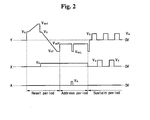
- Fig. 2 are driving waveforms of the plasma display according to the exemplary embodiment of the present invention.
- one subfield of the plurality of subfields is exemplarily described.
- the driving waveforms supplied to a Y electrode, an X electrode, and an A electrode are exemplarily described in connection with only one cell 110 (Fig. 1).
- one subfield is divided into the reset period, the address period, and the sustain period.
- the Y electrode driver 500 gradually increases a Y electrode voltage from a voltage V s to a voltage V set
- the A and X electrode drivers 300 and 400 respectively supply a ground voltage 0V to the A and X electrodes.
- a weak discharge is generated between the Y and X electrodes and between Y and A electrodes, and (-) wall charges are formed on the Y electrode and (+) wall charges are formed on the X and A electrodes.
- the Y electrode driver 500 gradually reduces the Y electrode voltage from the voltage V s to a voltage V nf while the X electrode driver 400 supplies a voltage V e to the X electrode, and an A electrode voltage is maintained at the ground voltage 0V. Then, a weak discharge is generated between the Y and X electrodes and between the Y and A electrodes while the voltage of the Y electrode is reduced, and accordingly the (-) wall charges formed on the Y electrode and the (+) wall charges formed on the X and A electrodes are eliminated. As a result, the wall charges formed on the cell can be initialized.
- the cell is initialized by gradually reducing the Y electrode voltage after gradually increasing the Y electrode in the reset period of Fig. 2, the cell may be initialized by another reset method.
- the Y and A electrode drivers 500 and 300 respectively supply a scan pulse of a voltage V scL and an address pulse of a voltage V a to the Y electrode and the A electrode to select the turned-on cell. Then, a discharge is generated in the cell receiving the scan pulse and the address pulse, and accordingly, the cell accumulates the wall charges to be set to the turned-on cell.
- the Y electrode driver 500 supplies a voltage V scH that is higher than the voltage V scL to a non-scanned Y electrode
- the A electrode driver 300 supplies the ground voltage 0V to a non-selected A electrode.
- the voltage V scH and the voltage V scL can be negative voltages.
- the Y electrode driver 500 supplies the scan pulse to the Y electrode in the first row (Y 1 of.Fig. 1).
- the A electrode driver 300 supplies the address pulse to the A electrode on the cells to be turned on along the first row.
- a discharge is generated between the Y electrode in the first row (Y 1 ) and the A electrode receiving the address pulse. Accordingly, (+) wall charges are formed on the Y electrode and (-) wall charges are formed on the A and X electrodes.
- the Y electrode driver 500 supplies the scan pulse to the Y electrode in a second row (Y 2 of Fig.
- the A electrode driver 300 supplies the address pulse to the A electrodes on the cells to be turned on along the second row. Then, the address discharge is generated in the cells crossed by the A electrodes receiving the address pulse and the Y electrode in the second row (Y 2 ), and accordingly wall charges are formed in those cells in the manner described above. Regarding Y electrodes in other rows, wall charges are formed in cells to be turned on in the same manner as described above, i.e., by supplying the address pulse to A electrodes on cells to be turned on while sequentially supplying the scan pulse to the Y electrodes from the first row (Y 1 of Fig. 1) to the last row (Y n of Fig. 1).
- the Y and X electrode drivers 500 and 400 respectively supply a pulse of the voltage V s and the ground voltage 0V to the Y and X electrodes, since the wall potential of the Y electrode is higher than the X electrode in the cells (the turned-on cells) having undergone the address discharge in the address period. As a result, a sustain discharge is generated between the Y and X electrodes of the turned-on cells.
- the sustain discharge the (-) wall charges are formed on the Y electrode and the (+) wall charges are formed on the X and A electrodes, such that the wall potential of the X electrode is higher than that of the Y electrode.
- the Y and X electrode drivers 500 and 400 respectively supply the ground voltage 0V and the pulse of the voltage V s to the Y and X electrodes, such that a subsequent sustain discharge is generated.
- (+) wall charges are again formed on the Y electrode and (-) wall charges are again formed on the X and A electrodes such that another sustain discharge can be generated by supplying the voltage V s to the Y electrode.
- the process of alternately supplying the pulse of the voltage V s to the Y electrode and supplying the pulse of the voltage V s is repeated a number of times corresponding to a weight of a corresponding subfield.
- a pulse that causes a voltage difference between the Y and X electrodes to be the voltage V s and the voltage -V s in turn can be supplied to the Y electrode and/or the X electrode.
- the cell can be set to be the turned-off cell through the address discharge in the address period after the cell accumulates the wall charges to be set to the turned-on cell in the reset period.
- a driving circuit for generating a driving waveform selected from among the driving waveforms of Fig. 2, which is supplied to the Y electrode during the address period, is described below with reference to Figs. 3 to 8.
- Fig. 3 is a circuit diagram of the Y electrode driver 500 according to the first exemplary embodiment of the present invention.
- a switch is depicted as an n-channel field effect transistor, but any other switch performing a similar function to that described below can be used instead of the n-channel field effect transistor.
- a gate driver for driving a gate of a transistor is not shown in Fig. 3.
- a circuit for supplying the reset waveform to the Y electrode in the reset period and a circuit for supplying the sustain pulse to the Y electrode in the sustain period are not shown, and these circuits are generally coupled to a node N2 of Fig. 3.
- the Y electrode driver 500 includes a plurality of scan circuits 510 1 to 510 n respectively coupled to the plurality of Y electrodes Y 1 to Y n , and a scan driving circuit 520.
- a i th scan circuit 510 i coupled to a i th Y electrode are only shown in Fig. 3
- Each scan circuit 510 i is coupled between a first node N1 and a second node N2, and includes two transistors M1 and M2.
- a contact point of the two transistors M1 and M2 is coupled to a corresponding Y electrode Y i .
- a source of the non-scan transistor M1 and a drain of the scan transistor M2 are coupled to the Y electrode Y i .
- a drain of the non-scan transistor M1 of the scan circuit 510 i is coupled to the first node N1, and a source of the scan transistor M2 of the scan circuit 510 i is coupled to the second node N2.
- k scan circuits corresponding to k Y electrodes of the plurality of Y electrodes Y 1 to Y n are fabricated as a scan integrated circuit (where 'k' is less than 'n'), and output terminals of the scan integrated circuit are respectively coupled to the k Y electrodes. If the number of the output terminals of the scan integrated circuit is less than 'n', a plurality of scan integrated circuits can be used while being coupled in parallel. The first node N1 and the second node N2 become input terminals of the scan integrated circuits.
- the scan driving circuit 520 includes a capacitor C1, a transistor Y scL , and a voltage divider 521.
- a first terminal of the capacitor C1 is coupled to the first node N1 of the scan circuits 510 1 to 510 n
- a second terminal of the capacitor C1 is coupled to the second node N2 of the scan circuits 510, to 510 n
- a drain of the transistor Y scL is coupled to the second node N2 of the scan circuits 510 1 to 510 n
- a source of the transistor Y scL is coupled to a voltage source for supplying a voltage V scL .
- the voltage divider 521 has an output terminal coupled to the first terminal N1 of the capacitor, and divides a voltage of a voltage source V sc and the voltage of the voltage source V scL and outputs a divided voltage to the output terminal.
- the voltage of the voltage source V sc is higher than the voltage V scL .
- a diode D1 can be coupled between the voltage source V sc and the voltage divider 521 to block a current path which is formed from the voltage divider 521 to the voltage source V sc .
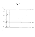
- the Y electrode driver 500 according to a second exemplary embodiment of the present invention is described below with reference to Fig. 4 and Fig. 5.
- Fig. 4 is a circuit diagram of the Y electrode driver 500 according to the second exemplary embodiment, and Fig. 5 are waveforms of the driving circuit of Fig. 4.
- a ground terminal 0 is used as the voltage source V sc in Fig. 4.
- a high level corresponds to a turned-on state of a transistor, and a low level corresponds to a turned-off state of the transistor.
- a voltage divider 521' includes resistors R1 and R2, and a transistor M3, in the second exemplary embodiment.
- a source of the transistor M3 is coupled to the first terminal of N1 of the capacitor C1, and a drain of the transistor M3 is coupled to the ground terminal 0.
- the resistor R1 is coupled between a gate of the transistor M3 and the drain of the transistor M3, and the resistor R2 is coupled between a source of the transistor Y scL and the gate of the transistor M3.
- a resistor R3 can be coupled between the ground terminal 0 and the drain of the transistor M3 to limit current flowing from the drain to the source of the transistor M3.
- the transistor Y scL is turned on during the address period such that a voltage of the second terminal N2 of the capacitor C1 becomes the voltage V scL .
- the ground voltage 0V and the voltage V scL are divided by the resistors R1 and R2 to be a gate voltage Vg of the transistor M3 as expressed in Equation 1 below.
- a source voltage of the transistor M3 becomes the voltage V scL since a voltage of the first terminal N1 of the capacitor C1 becomes the voltage V scL when a voltage has not been charged to the capacitor C1,. Therefore, a gate-source voltage Vgs of the transistor M3 is expressed in Equation 2 below.
- V ⁇ g R ⁇ 2 R ⁇ 1 + R ⁇ 2 V ⁇ s ⁇ c ⁇ L
- V ⁇ g ⁇ s 1 + R ⁇ 2 R ⁇ 1 + R ⁇ 2 ⁇ V ⁇ s ⁇ c ⁇ L
- a time in which the capacitor C1 is charged can be determined by controlling a magnitude of the resistor R3.
- a magnitude of the voltage V scH can be determined by having at least one of the resistors R1 and R2 be a variable resistor and controlling a magnitude of the variable resistor.
- Fig. 6 is a circuit diagram of a Y electrode driver 500' according to a third exemplary embodiment of the present invention.
- a scan driving circuit 520' of the Y electrode driver 500' generates the voltage V scH by using a linear regulator 522.
- the linear regulator 522 is coupled between the first terminal N1, i.e., the first node N1 of the scan circuit 510 i , and the voltage source V sc .
- a diode D1 can be coupled between the voltage source V sc and the linear regulator 522 to block a current path which is formed from the linear regulator 522 to the voltage source V sc .
- the linear regulator 522 lowers the voltage V sc and outputs the voltage V scH when the voltage of the first terminal N1 of the capacitor C1 is lower than the voltage V sc .
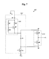
- Fig. 7 is a circuit diagram of a Y electrode driver 500' according to a fourth exemplary embodiment, and Fig. 8 are waveforms of the driving circuit of Fig. 7.
- a ground terminal 0 is used as the voltage source V sc in Fig. 7.
- a linear regulator 522' includes resistors R1' and R2', and a transistor M3'.
- a source of the transistor M3' is coupled to the first terminal of N1 of the capacitor C1, and a drain of the transistor M3' is coupled to the ground terminal 0.
- the resistor R1' is coupled between a gate of the transistor M3' and the drain of the transistor M3', and the resistor R2' is coupled between the source of the transistor M3 and the gate of the transistor M3.
- a resistor R3' can be coupled between the ground terminal 0 and the drain of the transistor M3 to limit current flowing from the drain of the transistor M3' to the source of the transistor M3'.
- the transistor Y scL is turned on during the address period such that a voltage of the second terminal N2 of the capacitor C1 becomes the voltage V scL .
- a voltage that is divided by the resistors R1' and R2' becomes a source voltage of the transistor M3' of the regulator 522 since a voltage of the first terminal N1 of the capacitor C1 is the voltage V scL if a voltage has not been charged to the capacitor C1. Therefore, a gate-source voltage Vgs' of the transistor M3' is given by Equation 5.
- the transistor M3' is turned on by the positive gate-source voltage Vgs' since the transistor M3' is the n-channel transistor.
- V ⁇ g ⁇ s ′ R ⁇ 2 R ⁇ 1 + R ⁇ 2 V ⁇ s ⁇ c ⁇ L
- a time in which the capacitor C1 is charged can be determined by controlling a magnitude of the resistor R3'.
- a magnitude of the voltage V scH can be determined by having at least one of the resistors R1' and R2' be a variable resistor and controlling a magnitude of the variable resistor.
- the voltage V scH CAN be set to a positive voltage by setting a voltage supplied from the voltage source V sc to a positive voltage.
- a voltage source supplying the voltage V a , V e , or V s of Fig. 2 can be used as this voltage source V sc .
- the voltage V scH can be generated by using a voltage generator such as the voltage divider and the linear regulator, the voltage source V sc (the ground terminal 0), and the voltage source V scL .
- the voltage generator generates the voltage V scH by controlling the source voltage of the transistor M3 or M3' by using the voltage charged to the capacitor C1. Therefore, the voltage V scH can be supplied to the Y electrodes during the address period without requiring a separate voltage source for supplying the voltage V scH .
Abstract
Description
- The present invention relates to a plasma display, a plasma display driver, and a method of driving a plasma display, and more particularly, to a driving circuit for driving a scan electrode of the plasma display.
- A plasma display is a display device that uses a plasma generated by gas discharge in discharge cells to display characters or images. Depending on its size, a Plasma Display Panel (PDP) of the plasma display includes more than several tens to millions of pixels arranged in a matrix pattern.
- One frame of the plasma display is divided into a plurality of subfields. Each subfield has a brightness weight and includes a reset period, an address period, and a sustain period. The reset period is for initializing the status of each discharge cell. The address period is for selecting turned-on/turned-off cells among the discharge cells, and the sustain period is for causing the turned-on cells to continue to discharge for displaying an image.
- In the plasma display, a discharge can be generated between two electrodes when a voltage difference between the two electrodes is greater than a predetermined voltage. Recently, the tendency has been to lower discharge voltages by using negative voltages since the discharge voltages are too high if all of the discharge voltages are set to positive voltages. Then, the discharge voltages can be lowered by using the negative voltages, but the number of voltage sources increase since the voltages of the reset period, the address period, and the sustain period are different.
- The present invention provides a plasma display and a plasma display driver and a method of driving the plasma display that reduce the number of voltage sources.
- An exemplary embodiment of the present invention is a plasma display including: a plurality of scan electrodes; a plurality of scan circuits respectively coupled to the plurality of scan electrodes, each scan circuit adapted to selectively supply a voltage of a first node and a voltage of a second node to a corresponding scan electrode of the plurality of scan electrodes; a capacitor coupled between the first node and the second node; a first transistor coupled between the second node and a first voltage source adapted to supply a first voltage; a second transistor coupled between a second voltage source adapted to supply a second voltage and the first node, and having a source whose voltage is determined by the first node; a first resistor coupled between the second voltage source and a gate of the second transistor; and a second resistor coupled to the gate of the second transistor, and adapted to divide the second voltage together with the first resistor.
- The second resistor is preferably coupled between the gate of the second transistor and a third voltage source.
- The third voltage source preferably includes the first voltage source.
- The second resistor is preferably coupled between the gate of the second transistor and the source of the second transistor.
- The second transistor is preferably an n-channel transistor, and the second voltage is preferably higher than the first voltage.
- The first voltage is a preferably negative voltage, and the second voltage is preferably a ground voltage.
- At least one of the first resistor and the second resistor preferably includes a variable resistor.
- The plasma display preferably further includes a diode and a third resistor coupled in series between the second voltage source and a drain of the second transistor; the first resistor is coupled between a contact point of the diode and the third resistor and the gate of the second transistor.
- Each scan circuit preferably includes: a third transistor coupled between the first node and the corresponding scan electrode; and a fourth transistor coupled between the corresponding scan electrode and the second node.
- The first transistor is preferably turned on, the fourth transistors of the plurality of scan circuits are preferably selectively turned on, and the third transistors of scan circuits having the turned-off fourth transistors are preferably turned on during the address period.
- At least part of the plurality of scan circuits preferably include an integrated circuit.
- Another exemplary embodiment of the present invention is a method of driving a plasma display including a plurality of scan electrodes, a plurality of scan circuits respectively coupled to the plurality of scan electrodes, and a capacitor coupled between the first terminal and the second terminal, each scan circuit selectively supplying a voltage of a first terminal and a voltage of a second terminal to a corresponding scan electrode of the plurality of scan electrodes, the driving method including: supplying a first voltage to the second terminal; supplying a second voltage that is higher than the first voltage to the first terminal to charge the capacitor; electrically isolating the second voltage from the capacitor upon the capacitor being charged such that a voltage of the first terminal is a third voltage; and selectively supplying the third voltage and the first voltage to the plurality of scan electrodes through the first terminals and the second terminals of the plurality of scan circuits.
- The second voltage is preferably higher than the third voltage. The first voltage is preferably a negative voltage, and the second voltage is preferably a ground voltage.
- Supplying the third voltage and the first voltage to the plurality of scan electrodes preferably includes: sequentially supplying the first voltage to the plurality of scan electrodes; and supplying the third voltage to those scan electrodes which the first voltage have not been supplied.
- Supplying the first voltage to the second terminal preferably includes supplying a voltage that is divided between a fourth voltage corresponding to the second voltage and the first voltage to a gate of a transistor having a source coupled to the first terminal; supplying the second voltage to the first terminal preferably includes turning on the transistor; and electrically isolating the second voltage from the capacitor preferably includes turning off the transistor.
- Supplying the first voltage to the second terminal preferably includes supplying a voltage that is divided between a fourth voltage corresponding to the second voltage and a voltage of the first terminal to a gate of a transistor having a source coupled to the first terminal; supplying the second voltage to the first terminal preferably includes turning on the transistor; and electrically isolating the second voltage from the capacitor preferably includes turning off the transistor.
- Still another exemplary embodiment of the present invention is plasma display driver for a plasma display including a plurality of scan electrodes and a plurality of scan circuits respectively coupled to the plurality of scan electrodes, each scan circuit selectively supplying a voltage of a first terminal and a voltage of a second terminal to a corresponding scan electrode of the plurality of scan electrodes, the plasma display driver including: a capacitor coupled between the first terminal and the second terminal; a first transistor coupled between the second terminal and a first voltage source and adapted to supply a first voltage; and a voltage divider coupled between the first voltage source and a second voltage source and adapted to supply a second voltage, and to output a third voltage that is lower than the second voltage to the first terminal.
- The voltage divider preferably includes: a second transistor having a source coupled to the first terminal and a drain coupled to the second voltage source; a first resistor coupled between a gate of the second transistor and the drain of the second transistor; and a second resistor coupled between the gate of the second transistor and a source of the first transistor.
- The first transistor is preferably adapted to be turned on during an address period.
- The first voltage is a negative voltage, and the second voltage is a ground voltage.
- Yet another exemplary embodiment of the present invention is a plasma display driver for a plasma display including a plurality of scan electrodes and a plurality of scan circuits respectively coupled to the plurality of scan electrodes, each scan circuit selectively supplying a voltage of a first terminal and a voltage of a second terminal to a corresponding scan electrode of the plurality of scan electrodes, the plasma display driver including: a capacitor coupled between the first terminal and the second terminal; a first transistor coupled between the second terminal and a first voltage source and adapted to supply a first voltage; and a linear regulator coupled between the first terminal and a second voltage source and adapted to supply a second voltage, and to output a third voltage that is lower than the second voltage to the first terminal.
- The linear regulator preferably includes: a second transistor having a source coupled to the first terminal and a drain coupled to the second voltage source; a first resistor coupled between a gate of the second transistor and the drain of the second transistor; and a second resistor coupled between the gate of the second transistor and the source of the second transistor.
- The first transistor is preferably adapted to be turned on during an address period.
- The first voltage is preferably a negative voltage, and the second voltage is preferably a ground voltage.
- A more complete appreciation of the present invention and many of the attendant advantages thereof, will be readily apparent as the present invention becomes better understood by reference to the following detailed description when considered in conjunction with the accompanying drawings in which like reference symbols indicate the same or similar components, wherein:
- Fig. 1 is a view of a plasma display according to an exemplary embodiment of the present invention.
- Fig. 2 are driving waveforms of the plasma display according to the exemplary embodiment of the present invention.
- Figs. 3, 4, 6, and 7 are respective circuit diagrams of Y electrode drivers according to first to fourth exemplary embodiments of the present invention.
- Figs. 5 and 8 are respective waveforms of the driving circuits of Figs. 4 and 7.
- In the following detailed description, only certain exemplary embodiments of the present invention are shown and described, simply by way of illustration. As those skilled in the art would realize, the described embodiments can be modified in various different ways, all without departing from the scope of the present invention.
- Accordingly, the drawings and description are to be regarded as illustrative in nature, and not restrictive. There may be parts shown in the drawings, or parts not shown in the drawings, that are not discussed in the specification as they are not essential to a complete understanding of the present invention. Like reference numerals designate like elements. Phrases such as "one thing is coupled to another" can refer to either "a first one is directly coupled to a second one" or "the first one is coupled to the second one with a third one provided therebetween".
- Wall charges described in embodiments of the present invention refer to charges formed on a wall of a discharge cell close to each electrode and accumulated on the electrode. The wall charge is described as being "formed" or "accumulated" on the electrode although the wall charges do not actually touch the electrodes. Furthermore, a wall voltage is a potential difference formed between the walls of the discharge cell by the wall charges.
- Fig. 1 is a view of a plasma display according to an exemplary embodiment of the present invention.
- As shown in Fig. 1, the plasma display includes a Plasma Display Panel (PDP) 100, a
controller 200, an address electrode driver (hereinafter referred to as an "A electrode driver") 300, a sustain electrode driver (hereinafter referred to as an "X electrode driver") 400, and a scan electrode driver (hereinafter referred to as a "Y electrode driver") 500. - The
PDP 100 include a plurality of address electrodes A1 to Am (hereinafter referred to as "A electrodes") extending in a column direction, and a plurality of scan electrodes Y1 to Yn and a plurality of sustain electrodes X1 to Xn (hereinafter respectively referred to as "Y electrodes" and "X electrodes"), each extending in a row direction. Generally, the respective X electrodes X1 to Xn correspond to the respective Y electrodes Y1 to Yn. The sub-pixel area delineating a discharge space where the A electrodes cross the Y and X electrodes forms a discharge cell (hereinafter referred to as a "cell") 110. - The
controller 200 receives an external image signal and outputs driving control signals. Thecontroller 200 divides a frame into a plurality of subfields having brightness weights. TheA electrode driver 300, theX electrode driver 400, and theY electrode driver 500 respectively supply driving voltages to the A electrodes A1 to Am, the X electrodes X1 to Xn, and the Y electrodes Y1 to Yn according to the driving control signals. - Fig. 2 are driving waveforms of the plasma display according to the exemplary embodiment of the present invention. In Fig. 2, one subfield of the plurality of subfields is exemplarily described. For convenience, the driving waveforms supplied to a Y electrode, an X electrode, and an A electrode are exemplarily described in connection with only one cell 110 (Fig. 1).
- As shown, one subfield is divided into the reset period, the address period, and the sustain period. During the reset period, the
Y electrode driver 500 gradually increases a Y electrode voltage from a voltage Vs to a voltage Vset, while the A andX electrode drivers - Subsequently, the
Y electrode driver 500 gradually reduces the Y electrode voltage from the voltage Vs to a voltage Vnf while theX electrode driver 400 supplies a voltage Ve to the X electrode, and an A electrode voltage is maintained at the ground voltage 0V. Then, a weak discharge is generated between the Y and X electrodes and between the Y and A electrodes while the voltage of the Y electrode is reduced, and accordingly the (-) wall charges formed on the Y electrode and the (+) wall charges formed on the X and A electrodes are eliminated. As a result, the wall charges formed on the cell can be initialized. - While it has been described that the cell is initialized by gradually reducing the Y electrode voltage after gradually increasing the Y electrode in the reset period of Fig. 2, the cell may be initialized by another reset method.
- During the address period, the Y and A
electrode drivers Y electrode driver 500 supplies a voltage VscH that is higher than the voltage VscL to a non-scanned Y electrode, and theA electrode driver 300 supplies the ground voltage 0V to a non-selected A electrode. The voltage VscH and the voltage VscL can be negative voltages. - In more detail, the
Y electrode driver 500 supplies the scan pulse to the Y electrode in the first row (Y1 of.Fig. 1). At the same time, theA electrode driver 300 supplies the address pulse to the A electrode on the cells to be turned on along the first row. Then, after a discharge is generated between the Y electrode in the first row (Y1) and the A electrode receiving the address pulse, a discharge is generated between the Y electrode and the X electrode. Accordingly, (+) wall charges are formed on the Y electrode and (-) wall charges are formed on the A and X electrodes. Subsequently, while theY electrode driver 500 supplies the scan pulse to the Y electrode in a second row (Y2 of Fig. 1), theA electrode driver 300 supplies the address pulse to the A electrodes on the cells to be turned on along the second row. Then, the address discharge is generated in the cells crossed by the A electrodes receiving the address pulse and the Y electrode in the second row (Y2), and accordingly wall charges are formed in those cells in the manner described above. Regarding Y electrodes in other rows, wall charges are formed in cells to be turned on in the same manner as described above, i.e., by supplying the address pulse to A electrodes on cells to be turned on while sequentially supplying the scan pulse to the Y electrodes from the first row (Y1 of Fig. 1) to the last row (Yn of Fig. 1). - During the sustain period, the Y and
X electrode drivers - Subsequently, the Y and
X electrode drivers - The process of alternately supplying the pulse of the voltage Vs to the Y electrode and supplying the pulse of the voltage Vs is repeated a number of times corresponding to a weight of a corresponding subfield.
- While the above exemplary embodiment has been described to supply the sustain pulse of the voltage Vs to the Y electrode and the X electrode in turn, a pulse that causes a voltage difference between the Y and X electrodes to be the voltage Vs and the voltage -Vs in turn can be supplied to the Y electrode and/or the X electrode.
- In addition, while the above exemplary embodiment has been described to set a cell to be the turned-on cell through the address discharge in the address period after erasing the wall charges to initialize the cell in the reset period, the cell can be set to be the turned-off cell through the address discharge in the address period after the cell accumulates the wall charges to be set to the turned-on cell in the reset period.
- Next, a driving circuit for generating a driving waveform, selected from among the driving waveforms of Fig. 2, which is supplied to the Y electrode during the address period, is described below with reference to Figs. 3 to 8.
- Fig. 3 is a circuit diagram of the
Y electrode driver 500 according to the first exemplary embodiment of the present invention. In Fig. 3, a switch is depicted as an n-channel field effect transistor, but any other switch performing a similar function to that described below can be used instead of the n-channel field effect transistor. In addition, a gate driver for driving a gate of a transistor is not shown in Fig. 3. Furthermore, a circuit for supplying the reset waveform to the Y electrode in the reset period and a circuit for supplying the sustain pulse to the Y electrode in the sustain period are not shown, and these circuits are generally coupled to a node N2 of Fig. 3. - As shown in Fig. 3, the
Y electrode driver 500 includes a plurality of scan circuits 5101 to 510n respectively coupled to the plurality of Y electrodes Y1 to Yn, and ascan driving circuit 520. For convenience of illustration, a ith scan circuit 510i coupled to a ith Y electrode are only shown in Fig. 3 - Each scan circuit 510i is coupled between a first node N1 and a second node N2, and includes two transistors M1 and M2. A contact point of the two transistors M1 and M2 is coupled to a corresponding Y electrode Yi. In more detail, a source of the non-scan transistor M1 and a drain of the scan transistor M2 are coupled to the Y electrode Yi. A drain of the non-scan transistor M1 of the scan circuit 510i is coupled to the first node N1, and a source of the scan transistor M2 of the scan circuit 510i is coupled to the second node N2. Generally, k scan circuits corresponding to k Y electrodes of the plurality of Y electrodes Y1 to Yn are fabricated as a scan integrated circuit (where 'k' is less than 'n'), and output terminals of the scan integrated circuit are respectively coupled to the k Y electrodes. If the number of the output terminals of the scan integrated circuit is less than 'n', a plurality of scan integrated circuits can be used while being coupled in parallel. The first node N1 and the second node N2 become input terminals of the scan integrated circuits.
- The
scan driving circuit 520 includes a capacitor C1, a transistor YscL, and avoltage divider 521. In detail, a first terminal of the capacitor C1 is coupled to the first node N1 of the scan circuits 5101 to 510n, and a second terminal of the capacitor C1 is coupled to the second node N2 of the scan circuits 510, to 510n. A drain of the transistor YscL is coupled to the second node N2 of the scan circuits 5101 to 510n, and a source of the transistor YscL is coupled to a voltage source for supplying a voltage VscL. - The
voltage divider 521 has an output terminal coupled to the first terminal N1 of the capacitor, and divides a voltage of a voltage source Vsc and the voltage of the voltage source VscL and outputs a divided voltage to the output terminal. The voltage of the voltage source Vsc is higher than the voltage VscL. A diode D1 can be coupled between the voltage source Vsc and thevoltage divider 521 to block a current path which is formed from thevoltage divider 521 to the voltage source Vsc. - The
Y electrode driver 500 according to a second exemplary embodiment of the present invention is described below with reference to Fig. 4 and Fig. 5. - Fig. 4 is a circuit diagram of the
Y electrode driver 500 according to the second exemplary embodiment, and Fig. 5 are waveforms of the driving circuit of Fig. 4. Aground terminal 0 is used as the voltage source Vsc in Fig. 4. In Fig. 5, a high level corresponds to a turned-on state of a transistor, and a low level corresponds to a turned-off state of the transistor. - As shown in Fig. 4, a voltage divider 521' includes resistors R1 and R2, and a transistor M3, in the second exemplary embodiment. A source of the transistor M3 is coupled to the first terminal of N1 of the capacitor C1, and a drain of the transistor M3 is coupled to the
ground terminal 0. The resistor R1 is coupled between a gate of the transistor M3 and the drain of the transistor M3, and the resistor R2 is coupled between a source of the transistor YscL and the gate of the transistor M3. In addition, a resistor R3 can be coupled between theground terminal 0 and the drain of the transistor M3 to limit current flowing from the drain to the source of the transistor M3. - Referring to Fig. 5, firstly, the transistor YscL is turned on during the address period such that a voltage of the second terminal N2 of the capacitor C1 becomes the voltage VscL. The ground voltage 0V and the voltage VscL are divided by the resistors R1 and R2 to be a gate voltage Vg of the transistor M3 as expressed in Equation 1 below. In addition, a source voltage of the transistor M3 becomes the voltage VscL since a voltage of the first terminal N1 of the capacitor C1 becomes the voltage VscL when a voltage has not been charged to the capacitor C1,. Therefore, a gate-source voltage Vgs of the transistor M3 is expressed in
Equation 2 below. Then, the transistor M3 is turned on by the positive gate-source voltage Vgs since the transistor M3 is an n-channel transistor. As a result, the capacitor C1 is charged through a path of theground terminal 0, the diode D1, the resistor R3, the transistor M3, the capacitor C1, the transistor YscL, and the voltage source VscL.

- When the capacitor C1 is charged such that the gate-source voltage Vgs of the transistor M3 is less than a threshold voltage VTH of the transistor M3 as expressed in Equation 3, the transistor M3 is turned off. As a result, the voltage VN1 of the first terminal N1 of the capacitor C1 as expressed in Equation 4, and this voltage VN1 becomes the voltage VscH. If the voltage VN1 of the first terminal N1 of the capacitor C1 is lowered by discharge of the capacitor C1, the transistor M3 is turned on again. Therefore, a voltage charged to the capacitor C1 can be maintained at a desired voltage during the address period in which the transistor YscL is turned on.


- A time in which the capacitor C1 is charged can be determined by controlling a magnitude of the resistor R3. In addition, a magnitude of the voltage VscH can be determined by having at least one of the resistors R1 and R2 be a variable resistor and controlling a magnitude of the variable resistor.
- As described above, while the first and second exemplary embodiments have been described as generating the voltage VscH by dividing the voltage Vsc and the voltage VscL, another circuit can be used to generate the voltage VscH instead of the voltage divider.
- Fig. 6 is a circuit diagram of a Y electrode driver 500' according to a third exemplary embodiment of the present invention.
- As shown in Fig. 6, a scan driving circuit 520' of the Y electrode driver 500' according to the third exemplary embodiment generates the voltage VscH by using a
linear regulator 522. - In detail, the
linear regulator 522 is coupled between the first terminal N1, i.e., the first node N1 of the scan circuit 510i, and the voltage source Vsc. In addition, a diode D1 can be coupled between the voltage source Vsc and thelinear regulator 522 to block a current path which is formed from thelinear regulator 522 to the voltage source Vsc. Thelinear regulator 522 lowers the voltage Vsc and outputs the voltage VscH when the voltage of the first terminal N1 of the capacitor C1 is lower than the voltage Vsc. - Fig. 7 is a circuit diagram of a Y electrode driver 500' according to a fourth exemplary embodiment, and Fig. 8 are waveforms of the driving circuit of Fig. 7. A
ground terminal 0 is used as the voltage source Vsc in Fig. 7. - As shown in Fig. 7, a linear regulator 522' includes resistors R1' and R2', and a transistor M3'. A source of the transistor M3' is coupled to the first terminal of N1 of the capacitor C1, and a drain of the transistor M3' is coupled to the
ground terminal 0. The resistor R1' is coupled between a gate of the transistor M3' and the drain of the transistor M3', and the resistor R2' is coupled between the source of the transistor M3 and the gate of the transistor M3. In addition, a resistor R3' can be coupled between theground terminal 0 and the drain of the transistor M3 to limit current flowing from the drain of the transistor M3' to the source of the transistor M3'. - Referring to Fig. 8, firstly, the transistor YscL is turned on during the address period such that a voltage of the second terminal N2 of the capacitor C1 becomes the voltage VscL. In addition, a voltage that is divided by the resistors R1' and R2' becomes a source voltage of the transistor M3' of the
regulator 522 since a voltage of the first terminal N1 of the capacitor C1 is the voltage VscL if a voltage has not been charged to the capacitor C1. Therefore, a gate-source voltage Vgs' of the transistor M3' is given by Equation 5. Then, the transistor M3' is turned on by the positive gate-source voltage Vgs' since the transistor M3' is the n-channel transistor. As a result, the capacitor C1 is charged through a path of theground terminal 0, the diode D1, the resistor R3', the transistor M3', the capacitor C1, the transistor YscL, and the voltage source VscL.
- When the capacitor C1 is charged such that the gate-source voltage Vgs' of the transistor M3' is less than a threshold voltage VTH' of the transistor M3' as expressed in Equation 6, the transistor M3' is turned off. As a result, the voltage VN1 of the first terminal N1 of the capacitor C1 is given in
Equation 7, and this voltage VN1 becomes the voltage VscH. If the voltage VN1 of the first terminal N1 of the capacitor C1 is lowered by discharge of the capacitor C1, the transistor M3' is turned on again. Therefore, a voltage charged to the capacitor C1 can be maintained at a desired voltage during the address period in which the transistor YscL is turned on.


- A time in which the capacitor C1 is charged can be determined by controlling a magnitude of the resistor R3'. In addition, a magnitude of the voltage VscH can be determined by having at least one of the resistors R1' and R2' be a variable resistor and controlling a magnitude of the variable resistor.
- While the first to fourth exemplary embodiments have been described to set the voltage VscH to a negative voltage, the voltage VscH CAN be set to a positive voltage by setting a voltage supplied from the voltage source Vsc to a positive voltage. A voltage source supplying the voltage Va, Ve, or Vs of Fig. 2 can be used as this voltage source Vsc.
- As described above, according to the exemplary embodiments of the present invention, the voltage VscH can be generated by using a voltage generator such as the voltage divider and the linear regulator, the voltage source Vsc (the ground terminal 0), and the voltage source VscL. The voltage generator generates the voltage VscH by controlling the source voltage of the transistor M3 or M3' by using the voltage charged to the capacitor C1. Therefore, the voltage VscH can be supplied to the Y electrodes during the address period without requiring a separate voltage source for supplying the voltage VscH.
- While the present invention has been described in connection with what is presently considered to be practical exemplary embodiments, it is to be understood that the present invention is not limited to the disclosed embodiments, but rather is intended to cover various modifications and equivalent arrangements included within the scope of the appended claims.
Claims (25)
- A plasma display, comprising:a plurality of scan electrodes;a plurality of scan circuits respectively coupled to the plurality of scan electrodes, each scan circuit adapted to selectively supply a voltage of a first node and a voltage of a second node to a corresponding scan electrode of the plurality of scan electrodes;a capacitor coupled between the first node and the second node;a first transistor coupled between the second node and a first voltage source adapted to supply a first voltage;a second transistor coupled between a second voltage source adapted to supply a second voltage and the first node, and having a source whose voltage is determined by the first node;a first resistor coupled between the second voltage source and a gate of the second transistor; anda second resistor coupled to the gate of the second transistor, and adapted to divide the second voltage together with the first resistor.
- A plasma display according to claim 1, wherein the second resistor is coupled between the gate of the second transistor and a third voltage source.
- A plasma display according to claim 2, wherein the third voltage source includes the first voltage source.
- A plasma display according to claim 1, wherein the second resistor is coupled between the gate of the second transistor and the source of the second transistor.
- A plasma display according to any preceding claim, wherein the second transistor comprises an n-channel transistor, and wherein the second voltage is higher than the first voltage.
- A plasma display according to claim 5, wherein the first voltage comprises a negative voltage, and wherein the second voltage comprises a ground voltage.
- A plasma display according to according to any preceding claim, wherein at least one of the first resistor and the second resistor comprises a variable resistor.
- A plasma display according to any preceding claim, further comprising a diode and a third resistor coupled in series between the second voltage source and a drain of the second transistor; wherein the first resistor is coupled between a contact point of the diode and the third resistor and the gate of the second transistor.
- A plasma display according to any preceding claim, wherein each scan circuit comprises:a third transistor coupled between the first node and the corresponding scan electrode; anda fourth transistor coupled between the corresponding scan electrode and the second node.
- A plasma display according to claim 9, wherein the first transistor is turned on, the fourth transistors of the plurality of scan circuits are selectively turned on, and the third transistors of scan circuits having the turned-off fourth transistors are turned on during the address period.
- A plasma display according to claim 9 or 10, wherein at least part of the plurality of scan circuits comprise an integrated circuit.
- A method of driving a plasma display including a plurality of scan electrodes, a plurality of scan circuits respectively coupled to the plurality of scan electrodes, and a capacitor coupled between the first terminal and the second terminal, each scan circuit selectively supplying a voltage of a first terminal and a voltage of a second terminal to a corresponding scan electrode of the plurality of scan electrodes, the driving method comprising:supplying a first voltage to the second terminal;supplying a second voltage that is higher than the first voltage to the first terminal to charge the capacitor;electrically isolating the second voltage from the capacitor upon the capacitor being charged such that a voltage of the first terminal is a third voltage; andselectively supplying the third voltage and the first voltage to the plurality of scan electrodes through the first terminals and the second terminals of the plurality of scan circuits.
- A method according to claim 12, wherein the second voltage is higher than the third voltage.
- A method according to claim 13, wherein the first voltage comprises a negative voltage, and the second voltage comprises a ground voltage.
- A method according to claim 12, wherein supplying the third voltage and the first voltage to the plurality of scan electrodes comprises:sequentially supplying the first voltage to the plurality of scan electrodes; andsupplying the third voltage to those scan electrodes which the first voltage have not been supplied.
- A method according to any one of claims 12 to 15, wherein:supplying the first voltage to the second terminal comprises supplying a voltage that is divided between a fourth voltage corresponding to the second voltage and the first voltage to a gate of a transistor having a source coupled to the first terminal;supplying the second voltage to the first terminal comprises turning on the transistor; andelectrically isolating the second voltage from the capacitor comprises turning off the transistor.
- A method according to any one of claims 12 to 16, wherein:supplying the first voltage to the second terminal comprises supplying a voltage that is divided between a fourth voltage corresponding to the second voltage and a voltage of the first terminal to a gate of a transistor having a source coupled to the first terminal;supplying the second voltage to the first terminal comprises turning on the transistor; andelectrically isolating the second voltage from the capacitor comprises turning off the transistor.
- A plasma display driver for a plasma display including a plurality of scan electrodes and a plurality of scan circuits respectively coupled to the plurality of scan electrodes, each scan circuit being arranged to selectively supply a voltage of a first terminal and a voltage of a second terminal to a corresponding scan electrode of the plurality of scan electrodes, the plasma display driver comprising:a capacitor coupled between the first terminal and the second terminal;a first transistor coupled between the second terminal and a first voltage source adapted to supply a first voltage; anda voltage divider coupled between the first voltage source and a second voltage source adapted to supply a second voltage, the voltage divider being adapted to output a third voltage that is lower than the second voltage to the first terminal.
- A plasma display driver according to claim 18, wherein the voltage divider comprises:a second transistor having a source coupled to the first terminal and a drain coupled to the second voltage source;a first resistor coupled between a gate of the second transistor and the drain of the second transistor; anda second resistor coupled between the gate of the second transistor and a source of the first transistor.
- A plasma display driver according to claim 18 or 19, wherein the first transistor is adapted to be turned on during an address period.
- A plasma display driver according to claim 20, wherein the first voltage comprises a negative voltage, and the second voltage comprises a ground voltage.
- A plasma display driver for a plasma display including a plurality of scan electrodes and a plurality of scan circuits respectively coupled to the plurality of scan electrodes, each scan circuit selectively supplying a voltage of a first terminal and a voltage of a second terminal to a corresponding scan electrode of the plurality of scan electrodes, the plasma display driver comprising:a capacitor coupled between the first terminal and the second terminal;a first transistor coupled between the second terminal and a first voltage source and adapted to supply a first voltage; anda linear regulator coupled between the first terminal and a second voltage source and adapted to supply a second voltage, the linear regulator being adapted to output a third voltage that is lower than the second voltage to the first terminal.
- A plasma display driver according to claim 22, wherein the linear regulator comprises:a second transistor having a source coupled to the first terminal and a drain coupled to the second voltage source;a first resistor coupled between a gate of the second transistor and the drain of the second transistor; anda second resistor coupled between the gate of the second transistor and the source of the second transistor.
- A plasma display driver according to claim 23, wherein the first transistor is adapted to be turned on during an address period.
- A plasma display driver according to claim 24, wherein the first voltage comprises a negative voltage, and the second voltage comprises a ground voltage.
Applications Claiming Priority (2)
| Application Number | Priority Date | Filing Date | Title |
|---|---|---|---|
| KR1020050070768A KR100612349B1 (en) | 2005-08-02 | 2005-08-02 | Plasma display and driving device and driving method thereof |
| KR1020050074778A KR100670149B1 (en) | 2005-08-16 | 2005-08-16 | Plasma display and driving device and driving method thereof |
Publications (2)
| Publication Number | Publication Date |
|---|---|
| EP1750245A2 true EP1750245A2 (en) | 2007-02-07 |
| EP1750245A3 EP1750245A3 (en) | 2009-04-01 |
Family
ID=37520845
Family Applications (1)
| Application Number | Title | Priority Date | Filing Date |
|---|---|---|---|
| EP06254046A Withdrawn EP1750245A3 (en) | 2005-08-02 | 2006-08-01 | Plasma display and plasma display driver and method of driving plasma display |
Country Status (2)
| Country | Link |
|---|---|
| US (1) | US7733304B2 (en) |
| EP (1) | EP1750245A3 (en) |
Cited By (2)
| Publication number | Priority date | Publication date | Assignee | Title |
|---|---|---|---|---|
| EP1898390A1 (en) | 2006-09-11 | 2008-03-12 | Samsung SDI Co., Ltd. | Plasma display and voltage generator thereof |
| EP1988532A1 (en) * | 2007-05-03 | 2008-11-05 | Samsung SDI Co., Ltd. | Plasma display and driving method thereof |
Families Citing this family (6)
| Publication number | Priority date | Publication date | Assignee | Title |
|---|---|---|---|---|
| KR100823482B1 (en) * | 2007-03-12 | 2008-04-21 | 삼성에스디아이 주식회사 | Plasma display device and driving apparatus thereof |
| KR100831010B1 (en) * | 2007-05-03 | 2008-05-20 | 삼성에스디아이 주식회사 | Plasma display and control method thereof |
| KR100879287B1 (en) * | 2007-08-02 | 2009-01-16 | 삼성에스디아이 주식회사 | Plasma display and voltage generator thereof |
| KR100913180B1 (en) * | 2007-11-26 | 2009-08-19 | 삼성에스디아이 주식회사 | Plasma display device and power supply thereof |
| JP5389730B2 (en) * | 2010-05-14 | 2014-01-15 | 株式会社デンソー | Discharge device for power conversion system |
| US20160331933A1 (en) * | 2015-05-14 | 2016-11-17 | Medtronic Cryocath Lp | Dual deflection pull wire ring |
Citations (1)
| Publication number | Priority date | Publication date | Assignee | Title |
|---|---|---|---|---|
| US6040827A (en) * | 1996-07-11 | 2000-03-21 | Hitachi, Ltd. | Driver circuit, driver integrated circuit, and display device and electronic device using the driver circuit and driver integrated circuit |
Family Cites Families (23)
| Publication number | Priority date | Publication date | Assignee | Title |
|---|---|---|---|---|
| JP2917279B2 (en) | 1988-11-30 | 1999-07-12 | 富士通株式会社 | Gas discharge panel |
| US6097357A (en) | 1990-11-28 | 2000-08-01 | Fujitsu Limited | Full color surface discharge type plasma display device |
| JP3259253B2 (en) | 1990-11-28 | 2002-02-25 | 富士通株式会社 | Gray scale driving method and gray scale driving apparatus for flat display device |
| DE69229684T2 (en) | 1991-12-20 | 1999-12-02 | Fujitsu Ltd | Method and device for controlling a display panel |
| EP0554172B1 (en) | 1992-01-28 | 1998-04-29 | Fujitsu Limited | Color surface discharge type plasma display device |
| JP3025598B2 (en) | 1993-04-30 | 2000-03-27 | 富士通株式会社 | Display driving device and display driving method |
| JP2891280B2 (en) | 1993-12-10 | 1999-05-17 | 富士通株式会社 | Driving device and driving method for flat display device |
| JP3163563B2 (en) | 1995-08-25 | 2001-05-08 | 富士通株式会社 | Surface discharge type plasma display panel and manufacturing method thereof |
| JP2845183B2 (en) | 1995-10-20 | 1999-01-13 | 富士通株式会社 | Gas discharge panel |
| JP3424587B2 (en) | 1998-06-18 | 2003-07-07 | 富士通株式会社 | Driving method of plasma display panel |
| JP4030685B2 (en) | 1999-07-30 | 2008-01-09 | 三星エスディアイ株式会社 | Plasma display and manufacturing method thereof |
| JP2001325888A (en) | 2000-03-09 | 2001-11-22 | Samsung Yokohama Research Institute Co Ltd | Plasma display and its manufacturing method |
| JP4612947B2 (en) | 2000-09-29 | 2011-01-12 | 日立プラズマディスプレイ株式会社 | Capacitive load driving circuit and plasma display device using the same |
| JP2002215089A (en) * | 2001-01-19 | 2002-07-31 | Fujitsu Hitachi Plasma Display Ltd | Device and method for driving planar display device |
| JP2002215087A (en) | 2001-01-19 | 2002-07-31 | Fujitsu Hitachi Plasma Display Ltd | Plasma display device and control method therefor |
| US6963174B2 (en) * | 2001-08-06 | 2005-11-08 | Samsung Sdi Co., Ltd. | Apparatus and method for driving a plasma display panel |
| TWI250498B (en) | 2001-12-07 | 2006-03-01 | Semiconductor Energy Lab | Display device and electric equipment using the same |
| JP3854173B2 (en) | 2002-02-27 | 2006-12-06 | 東北パイオニア株式会社 | Driving method of light emitting display panel and organic EL display device |
| KR100467452B1 (en) | 2002-07-16 | 2005-01-24 | 삼성에스디아이 주식회사 | Driving apparatus and method of plasma display panel |
| KR100484647B1 (en) | 2002-11-11 | 2005-04-20 | 삼성에스디아이 주식회사 | A driving apparatus and a method of plasma display panel |
| KR100560472B1 (en) | 2003-11-10 | 2006-03-13 | 삼성에스디아이 주식회사 | A plasma display panel, a driving apparatus and a driving method of the same |
| KR100578837B1 (en) | 2003-11-24 | 2006-05-11 | 삼성에스디아이 주식회사 | Driving apparatus and driving method of plasma display panel |
| JP2005181890A (en) * | 2003-12-22 | 2005-07-07 | Fujitsu Hitachi Plasma Display Ltd | Drive circuit and plasma display device |
-
2006
- 2006-07-05 US US11/480,445 patent/US7733304B2/en not_active Expired - Fee Related
- 2006-08-01 EP EP06254046A patent/EP1750245A3/en not_active Withdrawn
Patent Citations (1)
| Publication number | Priority date | Publication date | Assignee | Title |
|---|---|---|---|---|
| US6040827A (en) * | 1996-07-11 | 2000-03-21 | Hitachi, Ltd. | Driver circuit, driver integrated circuit, and display device and electronic device using the driver circuit and driver integrated circuit |
Cited By (2)
| Publication number | Priority date | Publication date | Assignee | Title |
|---|---|---|---|---|
| EP1898390A1 (en) | 2006-09-11 | 2008-03-12 | Samsung SDI Co., Ltd. | Plasma display and voltage generator thereof |
| EP1988532A1 (en) * | 2007-05-03 | 2008-11-05 | Samsung SDI Co., Ltd. | Plasma display and driving method thereof |
Also Published As
| Publication number | Publication date |
|---|---|
| US20070029942A1 (en) | 2007-02-08 |
| US7733304B2 (en) | 2010-06-08 |
| EP1750245A3 (en) | 2009-04-01 |
Similar Documents
| Publication | Publication Date | Title |
|---|---|---|
| EP1750245A2 (en) | Plasma display and plasma display driver and method of driving plasma display | |
| US7542020B2 (en) | Power supply device and plasma display device including power supply device | |
| US8203508B2 (en) | Plasma display device and driving method thereof | |
| US8159418B2 (en) | Plasma display and driving method thereof | |
| EP2045794B1 (en) | Plasma display and driving method | |
| US20080259069A1 (en) | Plasma display device and driving method thereof | |
| EP1898390A1 (en) | Plasma display and voltage generator thereof | |
| US7830338B2 (en) | Plasma display and driving method thereof | |
| US7755574B2 (en) | Plasma display and driving method thereof | |
| KR100863969B1 (en) | Plasma display, and driving method thereof | |
| KR100612349B1 (en) | Plasma display and driving device and driving method thereof | |
| KR100863966B1 (en) | Plasma display and driving method thereof | |
| KR100670149B1 (en) | Plasma display and driving device and driving method thereof | |
| US20080136807A1 (en) | Plasma display device and driving method thereof | |
| US20090040142A1 (en) | Plasma display device and method of driving the same | |
| KR100637513B1 (en) | Plasma display device and driving method thereof | |
| KR100796686B1 (en) | Plasma display, and driving device and method thereof | |
| US7616196B2 (en) | Plasma display device and driving method thereof | |
| US20080174587A1 (en) | Plasma display and driving method thereof | |
| US8570247B2 (en) | Plasma display device, and apparatus and method for driving the same | |
| EP2595138A1 (en) | Plasma display and driving method thereof | |
| US20080158100A1 (en) | Driving device for plasma display panel and plasma display device including the same | |
| KR20080002078A (en) | Plasma display device and driving apparatus thereof | |
| US20090140952A1 (en) | Plasma display device, power supply thereof and associated methods | |
| US20090040210A1 (en) | Scan electrode driver for a plasma display |
Legal Events
| Date | Code | Title | Description |
|---|---|---|---|
| PUAI | Public reference made under article 153(3) epc to a published international application that has entered the european phase |
Free format text: ORIGINAL CODE: 0009012 |
|
| 17P | Request for examination filed |
Effective date: 20060808 |
|
| AK | Designated contracting states |
Kind code of ref document: A2 Designated state(s): AT BE BG CH CY CZ DE DK EE ES FI FR GB GR HU IE IS IT LI LT LU LV MC NL PL PT RO SE SI SK TR |
|
| AX | Request for extension of the european patent |
Extension state: AL BA HR MK YU |
|
| PUAL | Search report despatched |
Free format text: ORIGINAL CODE: 0009013 |
|
| AK | Designated contracting states |
Kind code of ref document: A3 Designated state(s): AT BE BG CH CY CZ DE DK EE ES FI FR GB GR HU IE IS IT LI LT LU LV MC NL PL PT RO SE SI SK TR |
|
| AX | Request for extension of the european patent |
Extension state: AL BA HR MK RS |
|
| AKX | Designation fees paid |
Designated state(s): DE FR GB |
|
| 17Q | First examination report despatched |
Effective date: 20110422 |
|
| R17C | First examination report despatched (corrected) |
Effective date: 20110502 |
|
| STAA | Information on the status of an ep patent application or granted ep patent |
Free format text: STATUS: THE APPLICATION IS DEEMED TO BE WITHDRAWN |
|
| 18D | Application deemed to be withdrawn |
Effective date: 20150303 |