EP1750097A2 - Magnetic Sensor - Google Patents
Magnetic Sensor Download PDFInfo
- Publication number
- EP1750097A2 EP1750097A2 EP20060118432 EP06118432A EP1750097A2 EP 1750097 A2 EP1750097 A2 EP 1750097A2 EP 20060118432 EP20060118432 EP 20060118432 EP 06118432 A EP06118432 A EP 06118432A EP 1750097 A2 EP1750097 A2 EP 1750097A2
- Authority
- EP
- European Patent Office
- Prior art keywords
- film
- sensor
- protective film
- magnetic sensor
- elements
- Prior art date
- Legal status (The legal status is an assumption and is not a legal conclusion. Google has not performed a legal analysis and makes no representation as to the accuracy of the status listed.)
- Granted
Links
- 230000001681 protective effect Effects 0.000 claims abstract description 44
- 230000005389 magnetism Effects 0.000 claims abstract description 7
- 239000011229 interlayer Substances 0.000 claims description 31
- 238000002161 passivation Methods 0.000 claims description 29
- 239000000758 substrate Substances 0.000 claims description 11
- 230000000704 physical effect Effects 0.000 claims description 6
- 239000010408 film Substances 0.000 description 109
- 238000005530 etching Methods 0.000 description 9
- 238000000034 method Methods 0.000 description 8
- 238000009966 trimming Methods 0.000 description 7
- 229910052751 metal Inorganic materials 0.000 description 6
- 239000002184 metal Substances 0.000 description 6
- 238000010586 diagram Methods 0.000 description 5
- VYPSYNLAJGMNEJ-UHFFFAOYSA-N Silicium dioxide Chemical compound O=[Si]=O VYPSYNLAJGMNEJ-UHFFFAOYSA-N 0.000 description 4
- 150000004767 nitrides Chemical class 0.000 description 4
- 229910052581 Si3N4 Inorganic materials 0.000 description 3
- HQVNEWCFYHHQES-UHFFFAOYSA-N silicon nitride Chemical compound N12[Si]34N5[Si]62N3[Si]51N64 HQVNEWCFYHHQES-UHFFFAOYSA-N 0.000 description 3
- QXZUUHYBWMWJHK-UHFFFAOYSA-N [Co].[Ni] Chemical compound [Co].[Ni] QXZUUHYBWMWJHK-UHFFFAOYSA-N 0.000 description 2
- 230000015572 biosynthetic process Effects 0.000 description 2
- 239000010410 layer Substances 0.000 description 2
- 238000004519 manufacturing process Methods 0.000 description 2
- 239000000463 material Substances 0.000 description 2
- 230000000116 mitigating effect Effects 0.000 description 2
- 239000004065 semiconductor Substances 0.000 description 2
- 235000012239 silicon dioxide Nutrition 0.000 description 2
- 239000000377 silicon dioxide Substances 0.000 description 2
- JBRZTFJDHDCESZ-UHFFFAOYSA-N AsGa Chemical compound [As]#[Ga] JBRZTFJDHDCESZ-UHFFFAOYSA-N 0.000 description 1
- 229910000531 Co alloy Inorganic materials 0.000 description 1
- 229910001218 Gallium arsenide Inorganic materials 0.000 description 1
- 229910052782 aluminium Inorganic materials 0.000 description 1
- XAGFODPZIPBFFR-UHFFFAOYSA-N aluminium Chemical compound [Al] XAGFODPZIPBFFR-UHFFFAOYSA-N 0.000 description 1
- 238000010438 heat treatment Methods 0.000 description 1
- WPYVAWXEWQSOGY-UHFFFAOYSA-N indium antimonide Chemical compound [Sb]#[In] WPYVAWXEWQSOGY-UHFFFAOYSA-N 0.000 description 1
- 230000000977 initiatory effect Effects 0.000 description 1
- 238000009413 insulation Methods 0.000 description 1
- 229910000889 permalloy Inorganic materials 0.000 description 1
- 229910052710 silicon Inorganic materials 0.000 description 1
- 239000010703 silicon Substances 0.000 description 1
- 239000010409 thin film Substances 0.000 description 1
Images


Classifications
-
- G—PHYSICS
- G01—MEASURING; TESTING
- G01D—MEASURING NOT SPECIALLY ADAPTED FOR A SPECIFIC VARIABLE; ARRANGEMENTS FOR MEASURING TWO OR MORE VARIABLES NOT COVERED IN A SINGLE OTHER SUBCLASS; TARIFF METERING APPARATUS; MEASURING OR TESTING NOT OTHERWISE PROVIDED FOR
- G01D5/00—Mechanical means for transferring the output of a sensing member; Means for converting the output of a sensing member to another variable where the form or nature of the sensing member does not constrain the means for converting; Transducers not specially adapted for a specific variable
- G01D5/12—Mechanical means for transferring the output of a sensing member; Means for converting the output of a sensing member to another variable where the form or nature of the sensing member does not constrain the means for converting; Transducers not specially adapted for a specific variable using electric or magnetic means
- G01D5/14—Mechanical means for transferring the output of a sensing member; Means for converting the output of a sensing member to another variable where the form or nature of the sensing member does not constrain the means for converting; Transducers not specially adapted for a specific variable using electric or magnetic means influencing the magnitude of a current or voltage
- G01D5/142—Mechanical means for transferring the output of a sensing member; Means for converting the output of a sensing member to another variable where the form or nature of the sensing member does not constrain the means for converting; Transducers not specially adapted for a specific variable using electric or magnetic means influencing the magnitude of a current or voltage using Hall-effect devices
- G01D5/145—Mechanical means for transferring the output of a sensing member; Means for converting the output of a sensing member to another variable where the form or nature of the sensing member does not constrain the means for converting; Transducers not specially adapted for a specific variable using electric or magnetic means influencing the magnitude of a current or voltage using Hall-effect devices influenced by the relative movement between the Hall device and magnetic fields
-
- G—PHYSICS
- G01—MEASURING; TESTING
- G01R—MEASURING ELECTRIC VARIABLES; MEASURING MAGNETIC VARIABLES
- G01R33/00—Arrangements or instruments for measuring magnetic variables
- G01R33/02—Measuring direction or magnitude of magnetic fields or magnetic flux
- G01R33/06—Measuring direction or magnitude of magnetic fields or magnetic flux using galvano-magnetic devices
- G01R33/09—Magnetoresistive devices
- G01R33/093—Magnetoresistive devices using multilayer structures, e.g. giant magnetoresistance sensors
Definitions
- the present invention relates to a sensor for detecting a change in a physical property.
- a magnetic sensor is used as a steering wheel angle sensor to detect the rotational angle of a steering wheel.
- the magnetoresistance elements 31 to 34 of the magnetic sensor 1 has predetermined patterns so that the electrical resistances R1 to R4 become equal to one another. Accordingly, the magnetoresistance elements 31 to 34 are formed by etching a magnetoresistance element formation film in accordance with the predetermined patterns.
- the accuracy in film formation and etching affects, and causes differences, in the electrical resistances R1 to R4 of the magnetoresistance elements 31 to 34. Furthermore, it is difficult for the above equation to be satisfied just by improving these accuracies.
- the magnetoresistance elements 31 to 34 may be irradiated by a laser beam and heated to physically stabilize the magnetoresistance elements 31 to 34.
- a process using a laser beam heat treatment process
- a device for laser beam emission becomes necessary. This raises the manufacturing cost of the magnetic sensor 1.
- the present invention provides an inexpensive sensor for suppressing changes in the offset voltage that would be caused by wear.
- the present invention is a sensor for detecting a change in a physical property.
- the sensor includes a plurality of sensor elements, each having an electrical resistance that varies in accordance with a change in a physical property.
- a protective film covers the sensor elements.
- An etched portion is formed in at least part of the protective film.
- a further aspect of the present invention is a magnetic sensor for detecting rotational angle of a steering wheel.
- the magnetic sensor includes a substrate.
- An insulative film is formed on the substrate.
- a plurality of sensor elements are formed on the insulative film.
- Each of the sensor elements has an electrical resistance that varies in accordance with a magnetism change.
- a protective film covers the sensor elements.
- a recess is formed in the protective film near each of the sensor elements without exposing the sensor elements from the protective film.
- the magnetic sensor 1 is used for a steering wheel angle sensor in an automobile.
- the magnetic sensor 1 includes a substrate 10.
- the substrate 10 which is formed by a semiconductor (silicon in the preferred embodiment), has an upper surface coated by an insulative film 20.
- the insulative film 20 which is formed by an oxide film (a film of silicon dioxide in the preferred embodiment), covers substantially the entire upper surface of the substrate 10.
- Magnetoresistance elements 31 to 34 are arranged on the insulative film 20.
- the magnetoresistance elements 31 to 34 are each formed by a thin film having a predetermined pattern. Further, the magnetoresistance elements 31 to 34 are made of a nickel-cobalt, which is a ferromagnet having a negative magnetic property.
- An interlayer insulative film 40 is applied to the upper surface of the insulative film 20.
- the interlayer insulative film 40 covers most of the upper surface of the insulative film 20 and entirely covers the magnetoresistance elements 31 to 34.
- the interlayer insulative film 40 is made of a nitride film (a film of silicon nitride in the preferred embodiment).
- Metal pads 50 are arranged on the upper surface of the interlayer insulative film 40.
- the magnetoresistance elements 31 to 34 each have an initiating end and a terminating end, which are each connected to the lower surface of one of the metal pads 50.
- Each metal pad 50 has a partially exposed upper surface.
- the metal pads 50 are formed from aluminum.
- a passivation film is applied to the interlayer insulative film 40.
- the passivation film 60 covers most of the upper surface of the interlayer insulative film 40.
- the passivation film 60 is formed by a nitride film (a film of silicon nitride in the preferred embodiment).
- the substrate 10 The functions of the substrate 10, the insulative film 20, the magnetoresistance elements 31 to 34, the interlayer insulative film 40, the metal pads 50, and the passivation film 60 will now be discussed.
- the substrate 10 functions as a base for the magnetoresistance elements 31 to 34.
- the insulative film 20 functions to ensure the necessary level of insulation between the substrate 10 and the magnetoresistance elements 31 to 34.
- the insulative film 20 functions as an underlayer when arranging the magnetoresistance elements 31 to 34 on the substrate 10.
- the magnetoresistance elements 31 to 34 function as sensor elements of the magnetic sensor 1 for detecting magnetism changes.
- the magnetoresistance elements 31 to 34 have electrical resistances R1 to R4 that change in accordance with magnetism changes.
- the interlayer insulative film 40 functions as a protective film for protecting the magnetoresistance elements 31 to 34 from external disturbances.
- the metal pads 50 function as a medium for electrically connecting the magnetoresistance elements 31 to 34 with a wire bonding in the state shown in Fig. 3.
- the passivation film 60 functions as a protective film for protecting the magnetoresistance elements 31 to 34 from external disturbances.
- the interlayer insulative film 40 and the passivation film 60 form a protective film that covers the magnetoresistance elements 31 to 34.
- the protective film includes etched portions, or recesses 61. Each recess 61, which is formed by etching and eliminating parts of the protective film, extends to the insulative film 20.
- the recesses 61 are arranged so that they do not expose the magnetoresistance elements 31 to 34. Thus, the magnetoresistance elements 31 to 34 are each entirely covered by the protective film.
- the recesses 61 are arranged to surround each of the magnetoresistance elements 31 to 34, which are polygonal. When the magnetoresistance elements 31 to 34 are each rectangular, four of the recesses 61 are arranged, independent from one another, along the four sides of each of the rectangular magnetoresistance elements 31 to 34.
- a recess 61 may be arranged so as to extend along two sides of each of the magnetoresistance elements 31 to 34.
- two independent L-shaped recesses 61 are provided for each of the magnetoresistance elements 31 to 34.
- two independent recesses 61 may be formed along two sides (e.g., the two long sides) of each of the magnetoresistance elements 31 to 34.
- magnetoresistance elements 31 to 34 each have a rectangular outer shape
- four independent short recesses 61 may be formed along the four sides of each of the magnetoresistance elements 31 to 34.
- the recesses 61 may have any shape.
- the recesses 61 are arranged in a balanced manner.
- the protective film (interlayer insulative film 40 and passivation film 60) may be completely etched and eliminated. This ensures mitigation of the stress applied to the magnetoresistance elements 31 to 34 by the protective film (interlayer insulative film 40 and passivation film 60). Accordingly, changes in the electrical resistances R1 to R4 resulting from such stress are suppressed.
- the etching may be performed so that only part of the passivation film 60 is eliminated. In this case, the interlayer insulative film 40 does not undergo etching. If the magnetoresistance elements 31 to 34 are each covered by three or more layers of protective film, the etching may be performed so as to eliminate part of at least one layer of the protective film.
- part of the protective film may be etched and eliminated so as to form a thin portion 62 in the protective film.
- the etching may be performed to a depth that does not reach the insulative film 20. This optimally mitigates the stress applied to the magnetoresistance elements 31 to 34 by the protective film (interlayer insulative film 40 and passivation film 60). Accordingly, changes in the electrical resistances R1 to R4 resulting from such a stress are suppressed.
- the magnetoresistance elements 31 to 34 do not have to be formed from a nickel-cobalt alloy.
- the magnetoresistance elements 31 to 34 may be formed from a ferromagnet having a negative magnetic property, such as a permalloy.
- the magnetoresistance elements 31 to 34 do not necessarily have to be formed from a material having a negative magnetic property.
- the magnetoresistance elements 31 to 34 may be formed of a semiconductor having a positive magnetic property, such as indium antimonide and gallium arsenide.
- the insulative film 20 may be a nitride film (e.g., silicon nitride).
- the interlayer insulative film 40 may be an oxide film (e.g., silicon dioxide).
- the interlayer insulative film 40 and the passivation film 60 may be formed of different materials.
- the interlayer insulative film 40 may be a nitride film and the passivation film 60 may be an oxide film.
- the present invention is embodied in a sensor for detecting magnetism changes.
- the present invention may be applied to sensors for detecting a change in a physical property, such as light, heat, and pressure.
Abstract
Description
- The present invention relates to a sensor for detecting a change in a physical property.
- In an automobile, a magnetic sensor is used as a steering wheel angle sensor to detect the rotational angle of a steering wheel.
- Referring to Fig. 3, a
magnetic sensor 1 includes fourmagnetoresistance elements 31 to 34, which form a Wheatstone bridge. A voltage difference is produced between node N1 of themagnetoresistance elements magnetoresistance elements 33 and 34. If the voltage difference between nodes N1 and N2 (difference between median potentials E1 and E2 of the bridge, or offset voltage E12) is closer to 0 V in a state in which the magnetic field of themagnetic sensor 1 extends in a predetermined direction, themagnetic sensor 1 would have a higher capacity. More specifically, when R1, R2, R3, and R4 respectively represent the electrical resistances of themagnetoresistance elements - For the offset voltage E12 to be closer to 0 V, that is, for the above equation to be satisfied, the
magnetoresistance elements 31 to 34 of themagnetic sensor 1 has predetermined patterns so that the electrical resistances R1 to R4 become equal to one another. Accordingly, themagnetoresistance elements 31 to 34 are formed by etching a magnetoresistance element formation film in accordance with the predetermined patterns. However, the accuracy in film formation and etching affects, and causes differences, in the electrical resistances R1 to R4 of themagnetoresistance elements 31 to 34. Furthermore, it is difficult for the above equation to be satisfied just by improving these accuracies. - Accordingly, a trimming process for finely adjusting the electrical resistances R1 to R4 by trimming parts of the
magnetoresistance elements 31 to 34 has been proposed in the prior art (refer to, for example,Japanese Laid-Open Patent Publication No. 05-034224 - However, even when performing the trimming process to satisfy the above relationship, wear starts to progress at different rates in the
magnetoresistance elements 31 to 34 immediately after the trimming process. Thus, as time elapses, the Wheatstone bridge becomes imbalanced. As a result, the offset voltage E12 changes from 0 V soon after the trimming process to a level that affects the capacity of themagnetic sensor 1. Such a change cannot be ignored. - Accordingly, prior to the trimming process, the
magnetoresistance elements 31 to 34 may be irradiated by a laser beam and heated to physically stabilize themagnetoresistance elements 31 to 34. However, when a process using a laser beam (heat treatment process) is performed in addition to the trimming process, a device for laser beam emission becomes necessary. This raises the manufacturing cost of themagnetic sensor 1. - The present invention provides an inexpensive sensor for suppressing changes in the offset voltage that would be caused by wear.
- One aspect of the present invention is a sensor for detecting a change in a physical property. The sensor includes a plurality of sensor elements, each having an electrical resistance that varies in accordance with a change in a physical property. A protective film covers the sensor elements. An etched portion is formed in at least part of the protective film.
- A further aspect of the present invention is a magnetic sensor for detecting rotational angle of a steering wheel. The magnetic sensor includes a substrate. An insulative film is formed on the substrate. A plurality of sensor elements are formed on the insulative film. Each of the sensor elements has an electrical resistance that varies in accordance with a magnetism change. A protective film covers the sensor elements. A recess is formed in the protective film near each of the sensor elements without exposing the sensor elements from the protective film.
- Other aspects and advantages of the present invention will become apparent from the following description, taken in conjunction with the accompanying drawings, illustrating by way of example the principles of the invention.
- The invention, together with objects and advantages thereof, may best be understood by reference to the following description of the presently preferred embodiments together with the accompanying drawings in which:
- Fig. 1 is a plan view showing a magnetic sensor according to a first embodiment of the present invention;
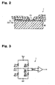
- Fig. 2 is a partial cross-sectional diagram of the magnetic sensor shown in Fig. 1;
- Fig. 3 is an electrical circuit diagram of a magnetic sensor;
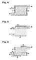
- Fig. 4 is a schematic plan view of a magnetic sensor according to a second embodiment of the present invention;
- Fig. 5 is a schematic plan view of a magnetic sensor according to a third embodiment of the present invention;
- Fig. 6 is a schematic plan view of a magnetic sensor according to a fourth embodiment of the present invention;
- Fig. 7 is a schematic plan view of a magnetic sensor according to a fifth embodiment of the present invention;
- Fig. 8 is a cross-sectional diagram of the magnetic sensor shown in Fig. 7;
- Fig. 9 is a cross-sectional diagram of a magnetic sensor according to a sixth embodiment of the present invention; and
- Fig. 10 is a cross-sectional diagram of a magnetic sensor according to a seventh embodiment of the present invention.
- A
magnetic sensor 1 according to a preferred embodiment of the present invention will now be discussed. Themagnetic sensor 1 is used for a steering wheel angle sensor in an automobile. - Referring to Figs. 1 and 2, the
magnetic sensor 1 includes asubstrate 10. Thesubstrate 10, which is formed by a semiconductor (silicon in the preferred embodiment), has an upper surface coated by aninsulative film 20. Theinsulative film 20, which is formed by an oxide film (a film of silicon dioxide in the preferred embodiment), covers substantially the entire upper surface of thesubstrate 10.Magnetoresistance elements 31 to 34 are arranged on theinsulative film 20. Themagnetoresistance elements 31 to 34 are each formed by a thin film having a predetermined pattern. Further, themagnetoresistance elements 31 to 34 are made of a nickel-cobalt, which is a ferromagnet having a negative magnetic property. - An interlayer
insulative film 40 is applied to the upper surface of theinsulative film 20. The interlayerinsulative film 40 covers most of the upper surface of theinsulative film 20 and entirely covers themagnetoresistance elements 31 to 34. Further, the interlayerinsulative film 40 is made of a nitride film (a film of silicon nitride in the preferred embodiment).Metal pads 50 are arranged on the upper surface of the interlayerinsulative film 40. Themagnetoresistance elements 31 to 34 each have an initiating end and a terminating end, which are each connected to the lower surface of one of themetal pads 50. Eachmetal pad 50 has a partially exposed upper surface. Themetal pads 50 are formed from aluminum. - A passivation film is applied to the interlayer
insulative film 40. Thepassivation film 60 covers most of the upper surface of the interlayerinsulative film 40. Thepassivation film 60 is formed by a nitride film (a film of silicon nitride in the preferred embodiment). - The functions of the
substrate 10, theinsulative film 20, themagnetoresistance elements 31 to 34, the interlayerinsulative film 40, themetal pads 50, and thepassivation film 60 will now be discussed. - The
substrate 10 functions as a base for themagnetoresistance elements 31 to 34. Theinsulative film 20 functions to ensure the necessary level of insulation between thesubstrate 10 and themagnetoresistance elements 31 to 34. In other words, theinsulative film 20 functions as an underlayer when arranging themagnetoresistance elements 31 to 34 on thesubstrate 10. Themagnetoresistance elements 31 to 34 function as sensor elements of themagnetic sensor 1 for detecting magnetism changes. Themagnetoresistance elements 31 to 34 have electrical resistances R1 to R4 that change in accordance with magnetism changes. Theinterlayer insulative film 40 functions as a protective film for protecting themagnetoresistance elements 31 to 34 from external disturbances. Themetal pads 50 function as a medium for electrically connecting themagnetoresistance elements 31 to 34 with a wire bonding in the state shown in Fig. 3. Thepassivation film 60 functions as a protective film for protecting themagnetoresistance elements 31 to 34 from external disturbances. - The features of the
magnetic sensor 1 will now be described. - The
interlayer insulative film 40 and thepassivation film 60 form a protective film that covers themagnetoresistance elements 31 to 34. The protective film (interlayer insulative film 40 and passivation film 60) include etched portions, or recesses 61. Eachrecess 61, which is formed by etching and eliminating parts of the protective film, extends to theinsulative film 20. Therecesses 61 are arranged so that they do not expose themagnetoresistance elements 31 to 34. Thus, themagnetoresistance elements 31 to 34 are each entirely covered by the protective film. Therecesses 61 are arranged to surround each of themagnetoresistance elements 31 to 34, which are polygonal. When themagnetoresistance elements 31 to 34 are each rectangular, four of therecesses 61 are arranged, independent from one another, along the four sides of each of therectangular magnetoresistance elements 31 to 34. - The advantages of the above embodiment will now be discussed.
- (1) The protective film (
interlayer insulative film 40 and passivation film 60), which cover themagnetoresistance elements 31 to 34, are etched and partially eliminated. This reduces the stress applied to themagnetoresistance elements 31 to 34 by the protective film (interlayer insulative film 40 and passivation film 60). Further, this suppresses changes in the electrical resistances R1 to R4 that would occur due to the stress that causes wear in themagnetoresistance elements 31 to 34. In other words, changes in the offset voltage 12 resulting from wear are suppressed. Additionally, the etching performed to eliminate parts of the protective film (interlayer insulative film 40 and passivation film 60) does not require a device for emitting a laser beam. This lowers the manufacturing costs. Accordingly, themagnetic sensor 1 is inexpensive and prevents changes in the offset voltage V12 that would be caused by wear. - (2) The protective film (
interlayer insulative film 40 and passivation film 60) are partially eliminated so that themagnetoresistance elements 31 to 34 are not exposed. That is, themagnetoresistance elements 31 to 34 are each maintained in a state protected by the protective film (interlayer insulative film 40 and passivation film 60). If themagnetoresistance elements 31 to 34 were not protected by the protective film (interlayer insulative film 40 and passivation film 60), external disturbances would cause wear that change the electrical resistances. However, this does not occur in the above embodiment. Accordingly, the full capacity of themagnetic sensor 1 may be utilized. - (3) The protective film (
interlayer insulative film 40 and passivation film 60) are eliminated along the surrounding of each of themagnetoresistance elements 31 to 34. This optimally mitigates the stress applied to themagnetoresistance elements 31 to 34 by the protective film (interlayer insulative film 40 and passivation film 60). Accordingly, changes in the electrical resistances R1 to R4 caused by stress are suppressed in an optimal manner. - (4) Parts of the protective film (
interlayer insulative film 40 and passivation film 60) are eliminated through etching to form therecesses 61, which extend to theinsulative film 20, in the protective film (interlayer insulative film 40 and passivation film 60). This ensures mitigation of the stress applied to themagnetoresistance elements 31 to 34 by the protective film (interlayer insulative film 40 and passivation film 60). Accordingly, changes in the electrical resistances R1 to R4 caused by stress are suppressed. - It should be apparent to those skilled in the art that the present invention may be embodied in many other specific forms without departing from the spirit or scope of the invention. Particularly, it should be understood that the present invention may be embodied in the following forms.
- Referring to Fig. 4, when the
magnetoresistance elements 31 to 34 each have a rectangular outer shape, arecess 61 may be arranged so as to extend along two sides of each of themagnetoresistance elements 31 to 34. In this case, two independent L-shapedrecesses 61 are provided for each of themagnetoresistance elements 31 to 34. - Referring to Fig. 5, when the
magnetoresistance elements 31 to 34 each have a rectangular outer shape, twoindependent recesses 61 may be formed along two sides (e.g., the two long sides) of each of themagnetoresistance elements 31 to 34. - Referring to Fig. 6, when the
magnetoresistance elements 31 to 34 each have a rectangular outer shape, four independentshort recesses 61 may be formed along the four sides of each of themagnetoresistance elements 31 to 34. - The
recesses 61 may have any shape. - It is preferred that the
recesses 61 are arranged in a balanced manner. - Referring to Figs. 7 and 8, excluding portions overlapping the
magnetoresistance elements 31 to 34, the protective film (interlayer insulative film 40 and passivation film 60) may be completely etched and eliminated. This ensures mitigation of the stress applied to themagnetoresistance elements 31 to 34 by the protective film (interlayer insulative film 40 and passivation film 60). Accordingly, changes in the electrical resistances R1 to R4 resulting from such stress are suppressed. - Referring to Fig. 9, the etching may be performed so that only part of the
passivation film 60 is eliminated. In this case, theinterlayer insulative film 40 does not undergo etching. If themagnetoresistance elements 31 to 34 are each covered by three or more layers of protective film, the etching may be performed so as to eliminate part of at least one layer of the protective film. - Referring to Fig. 10, part of the protective film (
interlayer insulative film 40 and passivation film 60) may be etched and eliminated so as to form athin portion 62 in the protective film. In other words, the etching may be performed to a depth that does not reach theinsulative film 20. This optimally mitigates the stress applied to themagnetoresistance elements 31 to 34 by the protective film (interlayer insulative film 40 and passivation film 60). Accordingly, changes in the electrical resistances R1 to R4 resulting from such a stress are suppressed. - The
magnetoresistance elements 31 to 34 do not have to be formed from a nickel-cobalt alloy. For example, themagnetoresistance elements 31 to 34 may be formed from a ferromagnet having a negative magnetic property, such as a permalloy. - The
magnetoresistance elements 31 to 34 do not necessarily have to be formed from a material having a negative magnetic property. For example, themagnetoresistance elements 31 to 34 may be formed of a semiconductor having a positive magnetic property, such as indium antimonide and gallium arsenide. - The
insulative film 20 may be a nitride film (e.g., silicon nitride). - The
interlayer insulative film 40 may be an oxide film (e.g., silicon dioxide). - The
interlayer insulative film 40 and thepassivation film 60 may be formed of different materials. For example, theinterlayer insulative film 40 may be a nitride film and thepassivation film 60 may be an oxide film. - The present invention is embodied in a sensor for detecting magnetism changes. For example, the present invention may be applied to sensors for detecting a change in a physical property, such as light, heat, and pressure.
- The present examples and embodiments are to be considered as illustrative and not restrictive, and the invention is not to be limited to the details given herein, but may be modified within the scope and equivalence of the appended claims.
Claims (15)
- A sensor for detecting a change in a physical property, wherein the sensor includes a plurality of sensor elements, each having an electrical resistance that varies in accordance with a change in a physical property, and a protective film for covering the sensor elements, the sensor being characterized by:an etched portion formed in at least part of the protective film.
- The sensor according to claim 1, characterized in that the etched portion is a recess formed near each of the sensor elements.
- The sensor according to claim 2, characterized in that the recess is formed along the periphery of each of the sensor elements.
- The sensor according to claim 2 or 3, characterized in that the recess forms a thin portion in the protective film.
- The sensor according to any one of claims 2 to 4, characterized in that the sensor elements are each polygonal and have a plurality of sides, and the recess is formed in correspondence with each of at least two of the sides of each sensor element.
- The sensor according to any one of claims 1 to 5, characterized in that the etched portion is formed in portions of the protective film excluding portions overlapped with the sensor elements.
- The sensor according to any one of claims 1 to 6, characterized in that the protective film includes a passivation film and an interlayer insulative film, and the etched portion is formed in at least part of the passivation film.
- The sensor according to any one of claims 1 to 7, further being characterized by:an insulative film on which the sensor elements are formed, wherein the etched portion is formed in the protective film so as to extend to the insulative film.
- A magnetic sensor for detecting rotational angle of a steering wheel, wherein the magnetic sensor includes a substrate, an insulative film formed on the substrate, a plurality of sensor elements formed on the insulative film, with each of the sensor elements having an electrical resistance that varies in accordance with a magnetism change, and a protective film for covering the sensor elements, the magnetic sensor being characterized by:a recess formed in the protective film near each of the sensor elements without exposing the sensor elements from the protective film.
- The magnetic sensor according to claim 9, characterized in that the recess is formed along the periphery of each of the sensor elements.
- The magnetic sensor according to claim 9 or 10, characterized in that the recess forms a thin portion in the protective film.
- The magnetic sensor according to any one of claims 9 to 11, characterized in that the sensor elements are each rectangular and have four sides, and the recess is formed in correspondence with each of at least two of the sides of each sensor element.
- The magnetic sensor according to any one of claims 9 to 12, characterized in that the etch.ed portion is formed in portions of the protective film excluding portions overlapped with the sensor elements.
- The magnetic sensor according to any one of claims 9 to 13, characterized in that the protective film includes a passivation film and an interlayer insulative film, and the etched portion is formed in at least part of the passivation film.
- The magnetic sensor according any one of claims 9 to 14, characterized in that the etched portion is formed in the protective film so as to extend to the insulative film.
Applications Claiming Priority (1)
| Application Number | Priority Date | Filing Date | Title |
|---|---|---|---|
| JP2005228847A JP4276645B2 (en) | 2005-08-05 | 2005-08-05 | Sensor device |
Publications (3)
| Publication Number | Publication Date |
|---|---|
| EP1750097A2 true EP1750097A2 (en) | 2007-02-07 |
| EP1750097A3 EP1750097A3 (en) | 2008-11-12 |
| EP1750097B1 EP1750097B1 (en) | 2015-10-14 |
Family
ID=37439159
Family Applications (1)
| Application Number | Title | Priority Date | Filing Date |
|---|---|---|---|
| EP06118432.1A Active EP1750097B1 (en) | 2005-08-05 | 2006-08-04 | Magnetic Sensor |
Country Status (3)
| Country | Link |
|---|---|
| US (1) | US7786726B2 (en) |
| EP (1) | EP1750097B1 (en) |
| JP (1) | JP4276645B2 (en) |
Cited By (1)
| Publication number | Priority date | Publication date | Assignee | Title |
|---|---|---|---|---|
| EP2159588A4 (en) * | 2007-06-19 | 2017-11-08 | Alps Electric Co., Ltd. | Magnetic detecting device, method for manufacturing magnetic detecting device, and angle detecting device, position detecting device and magnetic switch using the magnetic detecting device |
Families Citing this family (3)
| Publication number | Priority date | Publication date | Assignee | Title |
|---|---|---|---|---|
| JP5249150B2 (en) * | 2009-07-23 | 2013-07-31 | 株式会社東海理化電機製作所 | Manufacturing method of magnetic sensor and magnetic sensor |
| US8749005B1 (en) * | 2012-12-21 | 2014-06-10 | Allegro Microsystems, Llc | Magnetic field sensor and method of fabricating a magnetic field sensor having a plurality of vertical hall elements arranged in at least a portion of a polygonal shape |
| JP7093953B2 (en) | 2019-02-27 | 2022-07-01 | 株式会社デンソー | Semiconductor devices and their manufacturing methods |
Citations (1)
| Publication number | Priority date | Publication date | Assignee | Title |
|---|---|---|---|---|
| JPH0534224A (en) | 1991-07-29 | 1993-02-09 | Hokuriku Electric Ind Co Ltd | Transducer circuit and manufacture thereof |
Family Cites Families (11)
| Publication number | Priority date | Publication date | Assignee | Title |
|---|---|---|---|---|
| JP3456204B2 (en) | 2001-01-09 | 2003-10-14 | 日立金属株式会社 | Magnetic encoder |
| KR900004780B1 (en) | 1985-09-13 | 1990-07-05 | 후지쓰 가부시끼가이샤 | Phase detective apparatus using mangetic sensor |
| JPS6263811A (en) | 1985-09-13 | 1987-03-20 | Fujitsu Ltd | Potentiometer |
| JPH02103284A (en) | 1988-10-12 | 1990-04-16 | Nkk Corp | Method for liquefying coal |
| US5667879A (en) * | 1995-09-13 | 1997-09-16 | Honeywell Inc. | TaN/NiFe/TaN anisotropic magnetic sensor element |
| JP2001119083A (en) | 1999-10-18 | 2001-04-27 | Matsushita Electric Ind Co Ltd | Semiconductor magnetism detection element |
| JP4029376B2 (en) | 2000-09-28 | 2008-01-09 | 日立金属株式会社 | Magnetic sensor, method of manufacturing the same, and encoder |
| JP3498737B2 (en) * | 2001-01-24 | 2004-02-16 | ヤマハ株式会社 | Manufacturing method of magnetic sensor |
| JPWO2004025745A1 (en) | 2002-09-13 | 2006-01-12 | 松下電器産業株式会社 | Magnetoresistive element, method for producing the same, and method for using the same |
| JP2004363157A (en) * | 2003-06-02 | 2004-12-24 | Res Inst Electric Magnetic Alloys | Thin film magnetic sensor and its manufacturing method |
| JP2005221450A (en) * | 2004-02-09 | 2005-08-18 | Yamaha Corp | Physical quantity sensor |
-
2005
- 2005-08-05 JP JP2005228847A patent/JP4276645B2/en not_active Expired - Fee Related
-
2006
- 2006-08-01 US US11/497,559 patent/US7786726B2/en active Active
- 2006-08-04 EP EP06118432.1A patent/EP1750097B1/en active Active
Patent Citations (1)
| Publication number | Priority date | Publication date | Assignee | Title |
|---|---|---|---|---|
| JPH0534224A (en) | 1991-07-29 | 1993-02-09 | Hokuriku Electric Ind Co Ltd | Transducer circuit and manufacture thereof |
Cited By (1)
| Publication number | Priority date | Publication date | Assignee | Title |
|---|---|---|---|---|
| EP2159588A4 (en) * | 2007-06-19 | 2017-11-08 | Alps Electric Co., Ltd. | Magnetic detecting device, method for manufacturing magnetic detecting device, and angle detecting device, position detecting device and magnetic switch using the magnetic detecting device |
Also Published As
| Publication number | Publication date |
|---|---|
| EP1750097A3 (en) | 2008-11-12 |
| JP4276645B2 (en) | 2009-06-10 |
| US20070030000A1 (en) | 2007-02-08 |
| US7786726B2 (en) | 2010-08-31 |
| EP1750097B1 (en) | 2015-10-14 |
| JP2007046920A (en) | 2007-02-22 |
Similar Documents
| Publication | Publication Date | Title |
|---|---|---|
| US9570676B2 (en) | Method for manufacturing the magnetic field sensor module | |
| US8274166B2 (en) | Semiconductor device and method of manufacturing the same | |
| US10901049B2 (en) | Magnetic sensor and method for manufacturing said magnetic sensor | |
| JP2006329929A (en) | Semiconductor pressure sensor | |
| EP1750097B1 (en) | Magnetic Sensor | |
| EP2071349B1 (en) | Magnetism detector and its manufacturing method | |
| JP5161433B2 (en) | Sensor device | |
| CN108139287B (en) | Manufacturing catheter sensors | |
| CN105914293B (en) | Magnetic sensor and method for manufacturing the same | |
| JP5015498B2 (en) | Sensor device | |
| US11561145B2 (en) | Sensor membrane structure with insulating layer | |
| JP4574496B2 (en) | Sensor device | |
| JP5726260B2 (en) | Magnetic sensor and manufacturing method thereof | |
| JP5000665B2 (en) | Magnetic detection device and manufacturing method thereof | |
| US9964606B2 (en) | Sensor module and method of manufacture | |
| JP4893541B2 (en) | Magnetic sensor | |
| JP4550701B2 (en) | Sensor device | |
| JP3227465U (en) | Bonding pad structure | |
| US20160258975A1 (en) | Acceleration sensor | |
| JPH06232478A (en) | Semiconductor device | |
| JP2017103385A (en) | Semiconductor device | |
| JP2015169539A (en) | Tmr magnetic sensor and manufacturing method of the same | |
| JP2007078480A (en) | Sensor system | |
| JPH07235710A (en) | Magnetoresistive | |
| JP2007225306A (en) | Magnetic sensor apparatus |
Legal Events
| Date | Code | Title | Description |
|---|---|---|---|
| PUAI | Public reference made under article 153(3) epc to a published international application that has entered the european phase |
Free format text: ORIGINAL CODE: 0009012 |
|
| AK | Designated contracting states |
Kind code of ref document: A2 Designated state(s): AT BE BG CH CY CZ DE DK EE ES FI FR GB GR HU IE IS IT LI LT LU LV MC NL PL PT RO SE SI SK TR |
|
| AX | Request for extension of the european patent |
Extension state: AL BA HR MK YU |
|
| PUAL | Search report despatched |
Free format text: ORIGINAL CODE: 0009013 |
|
| AK | Designated contracting states |
Kind code of ref document: A3 Designated state(s): AT BE BG CH CY CZ DE DK EE ES FI FR GB GR HU IE IS IT LI LT LU LV MC NL PL PT RO SE SI SK TR |
|
| AX | Request for extension of the european patent |
Extension state: AL BA HR MK RS |
|
| RIC1 | Information provided on ipc code assigned before grant |
Ipc: G01D 5/16 20060101AFI20061128BHEP Ipc: G01R 33/09 20060101ALI20081007BHEP Ipc: H01L 43/08 20060101ALI20081007BHEP |
|
| 17P | Request for examination filed |
Effective date: 20090113 |
|
| 17Q | First examination report despatched |
Effective date: 20090309 |
|
| AKX | Designation fees paid |
Designated state(s): CZ DE FR GB SE |
|
| REG | Reference to a national code |
Ref country code: DE Ref legal event code: R079 Ref document number: 602006046909 Country of ref document: DE Free format text: PREVIOUS MAIN CLASS: G01D0005160000 Ipc: G01D0005140000 |
|
| RIC1 | Information provided on ipc code assigned before grant |
Ipc: G01D 5/14 20060101AFI20150129BHEP Ipc: G01R 33/09 20060101ALI20150129BHEP |
|
| GRAP | Despatch of communication of intention to grant a patent |
Free format text: ORIGINAL CODE: EPIDOSNIGR1 |
|
| INTG | Intention to grant announced |
Effective date: 20150326 |
|
| RIN1 | Information on inventor provided before grant (corrected) |
Inventor name: ISHIZAKI, YOICHI Inventor name: MINAGAWA, TORU Inventor name: KOGISO, KATSUYA Inventor name: SUZUKI, FUMIHIRO |
|
| GRAP | Despatch of communication of intention to grant a patent |
Free format text: ORIGINAL CODE: EPIDOSNIGR1 |
|
| INTG | Intention to grant announced |
Effective date: 20150630 |
|
| GRAS | Grant fee paid |
Free format text: ORIGINAL CODE: EPIDOSNIGR3 |
|
| GRAA | (expected) grant |
Free format text: ORIGINAL CODE: 0009210 |
|
| AK | Designated contracting states |
Kind code of ref document: B1 Designated state(s): CZ DE FR GB SE |
|
| REG | Reference to a national code |
Ref country code: GB Ref legal event code: FG4D |
|
| REG | Reference to a national code |
Ref country code: DE Ref legal event code: R096 Ref document number: 602006046909 Country of ref document: DE |
|
| REG | Reference to a national code |
Ref country code: SE Ref legal event code: TRGR |
|
| REG | Reference to a national code |
Ref country code: SE Ref legal event code: TRGR |
|
| REG | Reference to a national code |
Ref country code: FR Ref legal event code: PLFP Year of fee payment: 11 |
|
| REG | Reference to a national code |
Ref country code: DE Ref legal event code: R097 Ref document number: 602006046909 Country of ref document: DE |
|
| PLBE | No opposition filed within time limit |
Free format text: ORIGINAL CODE: 0009261 |
|
| STAA | Information on the status of an ep patent application or granted ep patent |
Free format text: STATUS: NO OPPOSITION FILED WITHIN TIME LIMIT |
|
| 26N | No opposition filed |
Effective date: 20160715 |
|
| REG | Reference to a national code |
Ref country code: FR Ref legal event code: PLFP Year of fee payment: 12 |
|
| REG | Reference to a national code |
Ref country code: FR Ref legal event code: PLFP Year of fee payment: 13 |
|
| REG | Reference to a national code |
Ref country code: DE Ref legal event code: R084 Ref document number: 602006046909 Country of ref document: DE |
|
| PGFP | Annual fee paid to national office [announced via postgrant information from national office to epo] |
Ref country code: GB Payment date: 20200722 Year of fee payment: 15 Ref country code: CZ Payment date: 20200730 Year of fee payment: 15 Ref country code: FR Payment date: 20200715 Year of fee payment: 15 |
|
| PGFP | Annual fee paid to national office [announced via postgrant information from national office to epo] |
Ref country code: SE Payment date: 20200811 Year of fee payment: 15 |
|
| REG | Reference to a national code |
Ref country code: SE Ref legal event code: EUG |
|
| GBPC | Gb: european patent ceased through non-payment of renewal fee |
Effective date: 20210804 |
|
| PG25 | Lapsed in a contracting state [announced via postgrant information from national office to epo] |
Ref country code: SE Free format text: LAPSE BECAUSE OF NON-PAYMENT OF DUE FEES Effective date: 20210805 Ref country code: CZ Free format text: LAPSE BECAUSE OF NON-PAYMENT OF DUE FEES Effective date: 20210804 |
|
| PG25 | Lapsed in a contracting state [announced via postgrant information from national office to epo] |
Ref country code: GB Free format text: LAPSE BECAUSE OF NON-PAYMENT OF DUE FEES Effective date: 20210804 Ref country code: FR Free format text: LAPSE BECAUSE OF NON-PAYMENT OF DUE FEES Effective date: 20210831 |
|
| PGFP | Annual fee paid to national office [announced via postgrant information from national office to epo] |
Ref country code: DE Payment date: 20230627 Year of fee payment: 18 |