EP1742275A1 - Integrated wiring member for solar cell module, solar cell module using the same and method for manufacturing them - Google Patents
Integrated wiring member for solar cell module, solar cell module using the same and method for manufacturing them Download PDFInfo
- Publication number
- EP1742275A1 EP1742275A1 EP05734438A EP05734438A EP1742275A1 EP 1742275 A1 EP1742275 A1 EP 1742275A1 EP 05734438 A EP05734438 A EP 05734438A EP 05734438 A EP05734438 A EP 05734438A EP 1742275 A1 EP1742275 A1 EP 1742275A1
- Authority
- EP
- European Patent Office
- Prior art keywords
- wiring member
- solar cell
- integrated
- coating
- wiring
- Prior art date
- Legal status (The legal status is an assumption and is not a legal conclusion. Google has not performed a legal analysis and makes no representation as to the accuracy of the status listed.)
- Withdrawn
Links
Images





















Classifications
-
- H—ELECTRICITY
- H10—SEMICONDUCTOR DEVICES; ELECTRIC SOLID-STATE DEVICES NOT OTHERWISE PROVIDED FOR
- H10F—INORGANIC SEMICONDUCTOR DEVICES SENSITIVE TO INFRARED RADIATION, LIGHT, ELECTROMAGNETIC RADIATION OF SHORTER WAVELENGTH OR CORPUSCULAR RADIATION
- H10F19/00—Integrated devices, or assemblies of multiple devices, comprising at least one photovoltaic cell covered by group H10F10/00, e.g. photovoltaic modules
- H10F19/90—Structures for connecting between photovoltaic cells, e.g. interconnections or insulating spacers
-
- H—ELECTRICITY
- H10—SEMICONDUCTOR DEVICES; ELECTRIC SOLID-STATE DEVICES NOT OTHERWISE PROVIDED FOR
- H10F—INORGANIC SEMICONDUCTOR DEVICES SENSITIVE TO INFRARED RADIATION, LIGHT, ELECTROMAGNETIC RADIATION OF SHORTER WAVELENGTH OR CORPUSCULAR RADIATION
- H10F77/00—Constructional details of devices covered by this subclass
- H10F77/93—Interconnections
- H10F77/933—Interconnections for devices having potential barriers
- H10F77/935—Interconnections for devices having potential barriers for photovoltaic devices or modules
- H10F77/937—Busbar structures for modules
-
- H—ELECTRICITY
- H10—SEMICONDUCTOR DEVICES; ELECTRIC SOLID-STATE DEVICES NOT OTHERWISE PROVIDED FOR
- H10F—INORGANIC SEMICONDUCTOR DEVICES SENSITIVE TO INFRARED RADIATION, LIGHT, ELECTROMAGNETIC RADIATION OF SHORTER WAVELENGTH OR CORPUSCULAR RADIATION
- H10F19/00—Integrated devices, or assemblies of multiple devices, comprising at least one photovoltaic cell covered by group H10F10/00, e.g. photovoltaic modules
- H10F19/90—Structures for connecting between photovoltaic cells, e.g. interconnections or insulating spacers
- H10F19/902—Structures for connecting between photovoltaic cells, e.g. interconnections or insulating spacers for series or parallel connection of photovoltaic cells
-
- Y—GENERAL TAGGING OF NEW TECHNOLOGICAL DEVELOPMENTS; GENERAL TAGGING OF CROSS-SECTIONAL TECHNOLOGIES SPANNING OVER SEVERAL SECTIONS OF THE IPC; TECHNICAL SUBJECTS COVERED BY FORMER USPC CROSS-REFERENCE ART COLLECTIONS [XRACs] AND DIGESTS
- Y02—TECHNOLOGIES OR APPLICATIONS FOR MITIGATION OR ADAPTATION AGAINST CLIMATE CHANGE
- Y02E—REDUCTION OF GREENHOUSE GAS [GHG] EMISSIONS, RELATED TO ENERGY GENERATION, TRANSMISSION OR DISTRIBUTION
- Y02E10/00—Energy generation through renewable energy sources
- Y02E10/50—Photovoltaic [PV] energy
Definitions
- the present invention relates to an integrated wiring member for a solar cell module, a solar cell module using the same, and manufacturing methods thereof.
- a typical solar cell module has the following structure. That is, a plurality of solar cells are arranged in line and are electrically connected to each other to thereby form a cell unit. Then, a plurality of cell units formed as described above are arranged side by side, and the adjoining solar cells located at respective both ends of the cell units are electrically connected to each other through solder-plated wiring members; thus, the solar cells arranged in a form of a matrix are entirely connected to each other in series.
- the solar cells and the wiring members are insulated from and protected from the outside by filling resin (EVA (Ethylene Vinyl Acetate) resin), an end-face sealing member (silicone resin) and the like.
- EVA resin has a thermoplastic property and is in a liquid state.
- a solar cell module is mainly used in an industrial facility.
- a solar cell module tends to be used in a common residence. Therefore, an aesthetic sense of a solar cell module for use in a common residence becomes important.
- a solder-plated wiring material having a silver-color surface is externally conspicuous on a solar cell module formed by a solar cell which is entirely dark in color.
- Japanese Patent Laying-Open No. 2003-86820 proposes a structure that a wiring member is partly coated with an insulative coating member in order to achieve a solar cell module with improved insulation performance and improved aesthetic sense.
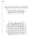
- a solar cell module 1 illustrated in Fig. 58 has the following structure. That is, as illustrated in Fig. 56, a plurality of solar cells 11 (nine in this example) are arranged in line and are electrically connected to each other through wiring members 12 to thereby form a cell unit 13 Then, a plurality of cell units 13 (six in this example) formed as described above are arranged side by side, and the adjoining solar cells (e.g., 11a1 and 11a2, 11b1 and 11b2, 11c1 and 11c2, 11d1 and 11d2, 11e1 and 11e2) located at respective both ends of the cell units are electrically connected to each other through wiring members 41, 42, 43, 44 and 45; thus, a group of solar cells arranged in a form of a matrix (hereinafter, simply referred to as "matrix”) 15 are entirely connected to each other in series.
- matrix hereinafter, simply referred to as "matrix”
- sheet-shaped filling resin (such as EVA) 16 and a back cover (back film) 17 are laminated on a bottom face of matrix 15 in which electrical connection is achieved.
- sheet-shaped filling resin (such as EVA) 18 and a front cover (glass) 19 are laminated on a top face (light receiving face) of matrix 15.
- a frame member 20 (not illustrated) made of aluminum surrounds outer peripheral edges of these components.
- Back cover 17, front cover 19, filling resin 16 and 18, and frame member 20 ensure strength performance, moisture-resistant performance and insulation performance.
- FIG. 57 (a) is a sectional view taken along a line A-A in (b) of Fig. 56, and partly illustrates cell unit 13 when being seen sideway.
- Each connecting member 12 includes a bent stage portion 12a, corresponding to a thickness of solar cell 11, formed at an almost center thereof. Through bent stage portion 12a, one connecting piece 12b is connected with a top face (negative electrode) 11a of solar cell 11 and the other connecting piece 12c is connected with a bottom face (positive electrode) 11b of adjoining solar cell 11.
- connecting member 12 is a rectangular-shaped flat copper wire having a solder-plated surface.
- Figs. 49, 50, 51, 52 and 53 are perspective views respectively illustrating wiring members 41, 42, 43, 44 and 45 each of which is obtained as follows: a rectangular-shaped flat copper wire having a solder-plated surface is partly coated with an insulative coating member.
- the adjoining solar cells e.g., 11a1 and 11a2, 11b1 and 11b2, 11c1 and 11c2, 11d1 and 11d2, 11e1 and 11e2 are connectable to each other.
- the wiring member is formed into an almost "L” shape or an almost "F” shape in accordance with a part where the adjoining solar cells are connected to each other.
- a shape of the wiring member is determined.
- Japanese Patent Laying-Open No. 2003-86820 there are required seven wiring members of five types in accordance with an arrangement method of solar cells 11, orientation of an electrode, a position of an electrical output extracting port, and the like.
- wiring member 41 includes a coupling piece 41a having a width of 6 mm and a thickness of 0.23 mm, and two protruding pieces 41b and 41b each having a width of 1.5 mm and a thickness of 0.15 mm.
- Protruding piece 41b connects coupling piece 41a to an electrode on a bottom face of each of solar cells 11a2, 11c2 and 11e2 (see Fig. 44).
- Wiring member 41 is formed into an almost "F" shape as a whole by connection by soldering between coupling piece 41a and protruding pieces 41 band 41b or by punching.
- Coupling piece 41a is entirely coated with an insulative coating member 411 (diagonally shaded).
- each of other wiring members 41, 42, 43, 44 and 45 is also formed into a predetermined shape by a combination of a coupling piece and protruding pieces, and predetermined portions are coated with a coating member.
- Fig. 54 illustrates examples of sectional structures of coated portions of wiring members 41, 42, 43, 44 and 45.
- dimensions of the respective components are described as one example. More specifically, a solder-plated copper wire having a width of 6 mm and a thickness of 0.23 mm, a solder-plated copper wire having a width of 1.5 mm and a thickness of 0.15 mm, and the like are formed by soldering into an almost "F" shape, an almost "E” shape, an almost “L” shape or the like; thus, integrated copper-wire formed bodies 41a to 45a are formed. Then, copper-wire formed bodies 41a to 45a are coated with films 411 to 451 such as a PET film, respectively. Films 411 to 451 are excellent in insulating performance and have various colors. This coating operation uses an adhesive, a double-faced tape or the like.
- the coating method as illustrated in Fig. 54, generally, one of insulating films 411 to 451 is folded in two and the copper-wire formed body is sandwiched therebetween. According to this method, a deviation of a copper-wire formed body is suppressed upon adhesion, and insulation performance is ensured.
- the copper-wire formed body is covered with EVA resin upon manufacturing of a solar cell module in a subsequent step. Therefore, completed wiring members 41, 42, 43, 44 and 45 must be previously subjected to vacuum lamination or deaeration in order to prevent generation of air bubbles in the EVA resin.
- an adhesive or a double-faced tape which does not exert an adverse influence on the EVA resin must be selected herein. Further, since wiring members 41, 42, 43, 44 and 45 are mainly connected by soldering, it is preferable that coating members 411 to 451 are excellent in heat-resistant property.
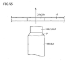
- each of a tip end of coating member 441 for coating protruding piece 44c of wiring member 44 in Fig. 52 and a tip end of coating member 451 for coating protruding piece 45c of wiring member 45 in Fig. 53 has a tapered face P cut obliquely.
- Tapered face P exhibits the following advantage. That is, when bare portion 44cl of wiring member 44 and bare portion 45cl of wiring member 45 are derived from electrical output extracting ports 25a and 25b formed in back cover 17 made of a conductive film to the outside, the tip ends (tapered faces P) of coating members 441 and 451 can smoothly pass through electrical output extracting ports 25a and 25b without catch in peripheral portions of electrical output extracting ports 25a and 25b.
- three first wiring members 41, 41 and 41 are arranged along the adjoining solar cells (e.g., 11a1 and 11a2, 11c1 and 11c2, 11e1 and 11e2) located at a side edge of matrix 15.
- bare portions 41a1 and 41 a2 of uppermost wiring member 41 are connected by soldering to the other connecting pieces 12c and 12c of connecting members 12 attached to solar cell 11a1 with the use of a soldering iron or the like.
- protruding pieces 41b and 41b of wiring member 41 are connected by soldering to an electrode on a bottom face of solar cell 11a2 with the use of a soldering iron or the like.
- middle wiring member 41 bare portions 41a1 and 41a2 of middle wiring member 41 are connected by soldering to the other connecting pieces 12c and 12c of connecting members 12 attached to solar cell 11c1 with the use of a soldering iron or the like. Then, protruding pieces 41b and 41b of wiring member 41 are connected by soldering to an electrode on a bottom face of solar cell 11c2 with the use of a soldering iron or the like.
- bare portions 41a1 and 41a2 of lowermost wiring member 41 are connected by soldering to the other connecting pieces 12c and 12c of connecting members 12 attached to solar cell 11e1 with the use of a soldering iron or the like.
- protruding pieces 41b and 41b of wiring member 41 are connected by soldering to an electrode on a bottom face of solar cell 11e2 with the use of a soldering iron or the like.
- circular marks indicate soldered connection portions.
- wiring member 42 is arranged along the adjoining solar cells (11b1 and 11b2) located at an upper center of an edge of matrix 15 (see Fig. 45).
- bare portions 42al and 42a2 of wiring member 42 are connected by soldering to the other connecting pieces 12c and 12c of connecting members 12 attached to solar cell 11b1 with the use of a soldering iron or the like.
- protruding pieces 42b and 42b of wiring member 42 are connected by soldering to an electrode on a bottom face of solar cell 1 lb2 with the use of a soldering iron or the like.
- wiring member 43 is arranged along the adjoining solar cells (11d1 and 11d2) located at a lower center of the edge of matrix 15 (see Fig. 45).
- bare portions 43al and 43a2 of wiring member 43 are connected by soldering to the other connecting pieces 12c and 12c of connecting members 12 attached to solar cell 11d1 with the use of a soldering iron or the like.
- protruding pieces 43b and 43b of wiring member 43 are connected by soldering to an electrode on a bottom face of solar cell 11d2 with the use of a soldering iron or the like.
- a bypass diode (not illustrated) is connected between a tip end 42c1 of protruding piece 42c of wiring member 42 and a tip end 43c1 of protruding piece 43c of wiring member 43.
- wiring member 44 is arranged so as to extend from the center of the side edge to an upper end in matrix 15 (see Fig. 46).
- protruding pieces 44b and 44b of wiring member 44 are connected by soldering to an electrode on a bottom face of solar cell 11f with the use of a soldering iron or the like.
- tip end 44c1 of protruding piece 44c of wiring member 44 is derived from electrical output extracting port 25a to the outside.
- wiring member 45 is arranged so as to extend from the center of the side edge to a lower end in matrix 15 (see Fig. 46).
- bare portions 45a1 and 45a2 of wiring member 45 are connected by soldering to the other connecting pieces 12c and 12c of connecting members 12 attached to solar cell 11g with the use of a soldering iron or the like.
- a tip end 45c1 of protruding piece 45c of wiring member 45 is derived from electrical output extracting port 25b to the outside.
- a bypass diode (not illustrated) is connected between tip end 42c1 of protruding piece 42c of wiring member 42 and tip end 44c1 of protruding piece 44c of wiring member 44.
- a bypass diode (not illustrated) is connected between tip end 43 cl of protruding piece 43c of wiring member 43 and tip end 45cl of protruding piece 45c of wiring member 45.
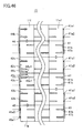
- Figs. 46 and 47 respectively illustrate a state after completion of the aforementioned wiring step.
- the other connecting pieces 12c, 12c, ... protruding from the side edge of matrix 15 are cut after completion of the wiring step (shown by broken lines in Fig. 46).
- Fig. 48 is a partly enlarged view illustrating a positional relation between wiring members near electrical output extracting ports 25a and 25b.
- circular marks indicate soldered connection portions.
- the number of soldered connection portions of wiring members 41, 42, 43, 44 and 45 formed as disclosed in Japanese Patent Laying-Open No. 2003-86820 is 24.
- wiring member 43 (45) for electrically connecting between the adjoining solar cells located at the both ends of the cell units intersects with wiring member 42 (44) for extracting an electrical output; therefore, a step of connecting a wiring member for connecting between adjoining solar cells and a step of connecting a wiring member for extracting an electrical output are implemented independently. Consequently, positional deviations of wiring members 42 and 44 or wiring members 44 and 45 are occurred, so that insulation performance failure due to a variation in outer appearance and a deviation in distance to a module end is occurred.
- a frequency of positional adjustment work must be increased in accordance with the number of wiring members in addition to the connection by soldering between the wiring member and the cell unit.
- a margin due to a positional deviation must be secured excessively and an area of a module region which does not contribute to power generation is increased, so that power generation efficiency per unit area as a solar cell module is lowered.
- wiring members 44 and 45 for extracting an electrical output are connected and fixed only by solar cells 11f and 11g located at the matrix end, the wiring members are flexed when being led out to the center of the solar cell module. Consequently, it is difficult to perform positional adjustment and to control arrangement of wiring members when the EVA resin filled into a mold is thermally solidified, so that a variation in outer appearance is occurred.
- wiring members 42 and 44 or wiring members 43 and 45 are simply integrated with each other.
- a coating member which has a color identical to that of back cover 17 and ensures a heat-resistant property is rare and expensive. Consequently, such a coating member is not practically used. That is, coating member 441, which is insufficient in heat-resistant property when connecting pieces 12c are connected by soldering to bare portions 42al and 42a2, is broken due to heat generated in the connection by soldering, resulting in insulation failure.
- connecting pieces 12c are connected by soldering to bare portions 42a1 and 42a2 from the back side of wiring member 44 in a state where wiring member 42 is integrally overlaid on the back side of the wiring member 44, protruding piece 44b must be arranged on the back face of solar cell 11f, connecting pieces 12c must be led out from the top face of solar cell 11b1 and must be arranged in bare portions 42a1 and 42a2, and protruding piece 44b must be arranged on the bottom face of solar cell 1 1b2. That is, it is necessary that a wiring member obtained by integrating wiring members 42 and 44 with each other is arranged so as to weave the front and back sides of adjoining cell units alternately, resulting in complicated work.
- wiring members 42 and 44 or wiring members 43 and 45 must be arranged in a division manner so as to suppress complication.
- Patent Document 1 Japanese Patent Laying-Open No. 2003-86820
- An object of the present invention is to provide an integrated wiring member for a solar cell module and a manufacturing method thereof, capable of facilitating a wiring step upon manufacturing a solar cell module, and achieving a solar cell module with improved insulation performance and improved aesthetic sense.
- the present invention provides an integrated wiring member for a solar cell module, including: a first wiring member; a second wiring member; and an insulating and protecting film for insulating the first wiring member and the second wiring member from each other, wherein the first wiring member and the second wiring member are integrated with each other through the insulating and protecting film.
- the first wiring member is coated with a first coating member
- the second wiring member is coated with a second coating member
- the first wiring member has a portion joined to a connecting member of a solar cell, and the portion is not coated with the first coating member.
- the second wiring member has a portion joined to a connecting member of a solar cell, and the portion is not covered with the second coating member.
- the first wiring member has a plurality of portions each joined to the connecting member of the solar cell, and the plurality of portions are spaced away from each other by a predetermined distance.
- the second wiring member has a plurality of portions each joined to the connecting member of the solar cell, and the plurality of portions are spaced away from each other by a predetermined distance.
- each of the first wiring member and the second wiring member has an almost “L” shape.
- the first wiring member is integrated with the second wiring member so as to have an almost "F" shape in such a manner that the first wiring member is displaced from a predetermined position with respect to the second wiring member.
- the insulating and protecting film is located between portions, which are not coated with the second coating member, of the second wiring member and between the first wiring member and the second wiring member.
- a portion, joined to the first wiring member, of the second wiring member is not coated with the second coating member and is integrated with the first wiring member through the insulating and protecting film.
- the insulating and protecting film is interposed between parts, each joined to a connecting member of a solar cell, of the second wiring member.
- the second wiring member is not coated with the second coating member, in a region of the second wiring member substantially overlapped with the first wiring member, the second wiring member, the insulating and protecting film and the first wiring member are integrally coated with a third coating member, and a region other than the region of the second wiring member is coated with the third coating member.
- the third coating member is not present in portions each joined to a connecting member of a solar cell, and the portions are spaced away from each other by a predetermined distance.
- the insulating and protecting film is interposed between portions each joined to the connecting member of the solar cell, and is also interposed between the first wiring member and the second wiring member.
- a region of the first wiring member substantially overlapped with the second wiring member is not coated with the first coating member and a region other than the region of the first wiring member is coated with the first coating member
- a region of the second wiring member substantially overlapped with the first wiring member is not coated with the second coating member and a region other than the region of the second wiring member is coated with the second coating member
- the first wiring member and the second wiring member are joined to each other through the insulating and protecting film
- the first wiring member, the second wiring member and the insulating and protecting film are integrally coated with the third coating member.
- portions each joined to a connecting member of a solar cell module have no coating member.
- each of the first wiring member and the second wiring member has an almost "T" shape.
- the first wiring member is integrated with the second wiring member so as to have an almost " ⁇ " shape in such a manner that the first wiring member is displaced from a predetermined position with respect to the second wiring member.
- the insulating and protecting film is a heat-resistant film.
- the insulating and protecting film has a width equal to or narrower than that of the first coating member.
- the second wiring member has a width equal to or narrower than that of the insulating and protecting film.
- the insulating and protecting film has a width equal to that of the first coating member or wider than that of the second wiring member.
- each of the first coating member, the second coating member and the third coating member has an insulation property.
- the present invention also provides a solar cell module having a structure that a plurality of solar cells are arranged in line and are electrically connected to each other to thereby form a cell unit, a plurality of cell units thus formed are arranged side by side, the adjoining solar cells located at respective both ends of the cell units are electrically connected to each other through a wiring member, and the solar cells arranged in a form of a matrix are entirely connected, wherein the aforementioned integrated wiring member is used as the wiring member.
- the integrated wiring member includes a first wiring member connected to a positive electrode of the solar cell module, and a second wiring member connected to a negative electrode of the solar cell module.
- the present invention also provides a manufacturing method of an integrated wiring member for a solar cell module, including the steps of: forming each of a first wiring member and a second wiring member into an almost "L" shape; partly coating the first wiring member with a first coating member; forming an insulating and protecting film on one face of the first wiring member so as to partly coat the first wiring member with the insulating and protecting film; folding back the insulating and protecting film toward the other face; joining a second wiring member to a face, opposite to the folded side of the insulating and protecting film, through the insulating and protecting film; partly coating the second wiring member with a second coating member; and integrally coating the first wiring member and the second wiring member with a third coating member.
- the present invention also provides a manufacturing method of a solar cell module, including the steps of arranging a plurality of solar cells in line and electrically connecting the plurality of solar cells to each other to thereby form a cell unit; arranging a plurality of cell units thus formed side by side, and electrically connecting the adjoining solar cells located at one ends of the cell units through a third integrated wiring member; electrically connecting between the adjoining solar cells through a first integrated wiring member having output terminals with positive electrodes located at the other ends of the cell units, and electrically connecting the output terminals with positive electrodes to the adjoining solar cells; and electrically connecting between the adjoining solar cells through a second integrated wiring member having output terminals with negative electrodes located at the other ends of the cell units, and electrically connecting the output terminals with negative electrodes to the adjoining solar cells.
- the present invention also provides a manufacturing method of a solar cell module, including the steps of: arranging a plurality of solar cells in line and electrically connecting the plurality of solar cells to each other to thereby form a cell unit; arranging a plurality of cell units thus formed side by side and electrically connecting wires led out from the adjoining solar cells located at one ends of the cell units to a third integrated wiring member, by soldering; and connecting positive electrode wires led out from solar cells located at the other ends of the cell units and wires led out from the adjoining solar cells to a first integrated wiring member, by soldering, and electrically connecting negative electrode wires led out from the solar cells located at the other ends of the cell units and wires led out from the adjoining solar cells to a second integrated wiring member, by soldering.
- the present invention also provides a manufacturing method of an integrated wiring member for a solar cell module, including the steps of: forming each of a first wiring member and a second wiring member into an almost "T" shape; partly coating the first wiring member with a first coating member; forming an insulating and protecting film on one side of the first wiring member so as to partly coat the first wiring member with the insulating and protecting film; folding back the insulating and protecting film toward the other side of the first wiring member; joining a second wiring member to a face, opposite to the folded side of the insulating and protecting film, through the insulating and protecting film; partly coating the second wiring member with a second coating member; and integrally coating the first wiring member and the second wiring member with a third coating member.
- the present invention also provides a manufacturing method of a solar cell module, including the steps of: arranging a plurality of solar cells in line and electrically connecting the plurality of solar cells to each other to thereby form a cell unit; arranging a plurality of cell units thus formed side by side, and electrically connecting between the adjoining solar cells located at one ends of the cell units through a third integrated wiring member; and electrically connecting between the adjoining solar cells through a fourth integrated wiring member which is located at the other ends of the cell units and includes output terminals with positive electrodes and output terminals with negative electrodes, and electrically connecting the output terminals with positive electrodes and the output terminals with negative electrodes to external terminals of the solar cells.
- the present invention also provides a manufacturing method of a solar cell module, including the steps of: arranging a plurality of solar cells in line and electrically connecting the plurality of solar cells to each other to thereby form a cell unit; arranging a plurality of cell units thus formed side by side, and electrically connecting wires led out from the adjoining solar cells located at one ends of the cell units to a third integrated wiring member, by soldering; and connecting positive electrode wires led out from solar cells located at the other ends of the cell units and wires led out from the adjoining solar cells to a fourth integrated wiring member, by soldering, and electrically connecting negative electrode wires led out from the solar cells located at the other ends of the cell units and wires led out from the adjoining solar cells to the fourth integrated wiring member, by soldering.
- the present invention it is possible to realize a solar cell module with reduced external variation and improved aesthetic sense. Further, it is possible to suppress insulation performance failure due to a variation in distance to a module end, and to improve an insulation property of a solar cell module.
- a portion, other than a connection portion, of a wiring member or at least a part of the portion is coated with an insulative coating member, so that improved insulation performance and improved aesthetic sense can be achieved.
- this coating member is allowed to have a color identical to those of peripheral members. As a result, the coating member is assimilated into the surface of the solar cell module; thus, an aesthetic sense can be further improved.
- an end-face sealing member for the solar cell module there is used silicone resin, EVA resin, an elastomer or the like which enters a liquid state once upon manufacturing of the solar cell module. Therefore, even when generation of air bubbles or separation occurs, a wiring member is coated with an insulative coating member, so that insulation performance between the wiring member and peripheral members can be ensured sufficiently.
- the solar cell module according to the present invention is formed into such a shape that a wiring member connecting between adjoining solar cells is connectable, so that work for connection by soldering in a wiring step in a solar cell module production process can be facilitated and a time for the work can be significantly reduced.
- a wiring member is formed in accordance with a shape of a connection part, the wiring member is arranged in the connection part, and a connection terminal of a solar cell is connected by soldering to a connection portion of the wiring member. More specifically, formed wiring members are integrated with each other, so that work for connection by soldering in a wiring step in a solar cell module production process can be facilitated and a time for the work can be significantly reduced.
- Arrangement of electrodes from a plurality of cell units arranged side by side is, for example, positive, negative, negative, positive, positive, negative, negative, positive; thus, the cell units can be connected in parallel through the integrated wiring member according to the present invention. Accordingly, a solar cell module obtaining a current twice in amount can be provided.
- arrangement of electrodes from a plurality of cell units arranged side by side is, for example, positive, negative, negative, positive, positive, negative, negative, positive, wherein identical polarities adjoin to each other; thus, an integrated wiring member can be connected. That is, in order to provide a solar cell module in which cell units are connected in parallel, there is adopted a mirror arrangement (e.g., positive, negative, negative, positive in a lateral direction) which is different in lateral arrangement of cells from the conventional technique; thus, an integrated wiring member can be connected.
- a mirror arrangement e.g., positive, negative, negative, positive in a lateral direction
- a solar cell module has the following structure. That is, a plurality of solar cells 11 are arranged in line and are electrically connected to each other to thereby form a cell unit 13. Then, a plurality of cell units 13 formed as described above are arranged side by side, and the adjoining solar cells (e.g., 11a1 and 11a2, 11b1 and 11b2, and the like) located at respective both ends of cell units 13 are electrically connected to each other through integrated wiring members 46, 47 and 48; thus, the solar cells arranged in a form of a matrix 15 are entirely connected to each other in series.
- each of wiring members 46, 47 and 48 for electrically connecting between the solar cells is of an integrated type, unlike a conventional wiring member.
- a portion other than a connection portion, in which solar cells of the wiring member are electrically connected to each other, is at least partly coated with an insulative coating member.
- a plurality of wiring members are used.
- One wiring member intersects with or overlaps with the other wiring member.
- one wiring member is coated with the coating member and the other wiring member has at least a connection portion.
- a coating member having a heat-resistant property higher than that of the aforementioned coating member is inserted between one wiring member and the other wiring member.
- use of the integrated wiring member according to the present invention makes it possible to improve insulation performance without breakage of a coating member when solar cells are electrically connected to each other by soldering of the connection portion of the wiring member. Further, a plurality of wiring members can be intersected with each other or overlapped with each other prior to the connection by soldering; therefore, a manufacturing step can be simplified. In addition, an area of a wiring member, exposed by overlapping wiring members, can be reduced, so that an aesthetic sense can be improved.
- the wiring member is a flat conductive wire, an outer appearance thereof becomes poor due to a wide width.
- the wiring member becomes inconspicuous.
- the coating member is allowed to have a color identical to those of peripheral members, so that the coating member is assimilated into the surface of the solar cell module.
- an aesthetic sense can be further improved.
- the coating member is allowed to have a color different from those of the peripheral members, so that a factor in terms of a design is added.
- an aesthetic sense can be also improved.
- the aforementioned resin Upon manufacturing a solar cell module while using silicone resin or EVA resin as an end-face sealing member for the solar cell module, the aforementioned resin enters a liquid state in course of the manufacturing. Therefore, use of only this resin tends to cause generation of air bubbles, separation and the like. In the present invention, however, at least one of adjacent wiring members is coated with an insulative member; therefore, insulation performance between two wiring members can be ensured sufficiently.
- a wiring member at least including a wire for extracting an electrical output is formed into an almost "L” shape so as to extract the electrical output from a bottom face near a center of the solar cell module.
- a wiring member for electrically connecting between adjoining solar cells is formed into a shape so as to connect between the solar cells.
- the wiring member is formed into an almost "I" shape in accordance with the connection part.
- a wiring member which connects between solar cells and is connected to a bypass diode is formed into a shape so as to connect between the solar cells and to be connected to the bypass diode.
- the wiring member is formed into an almost "L" shape.
- the almost “L”-shaped wiring member connecting between solar cells and the almost “L”-shaped wiring member at least including a wire for extracting an electrical output are partly overlapped with and intersected with each other. Further, it is preferable that the almost “L”-shaped wiring members are integrated with each other to form an almost “F” shape. As described above, a plurality of wiring member at least partly overlapped with or intersected with each other are integrated into one member; thus, work for connection by soldering in a wiring step in a solar cell module production process can be simplified and a time for the work can be reduced significantly.
- a manufacturing method of a solar cell module includes a first step of arranging a plurality of solar cells in line and electrically connecting the plurality of solar cells to each other to thereby form a cell unit, and a second step of arranging a plurality of cell units, formed as described above, side by side and electrically connecting the adjoining solar cells, located at respective both ends of the cell units, to each other through integrated wiring members.
- the first step includes a step of forming a connecting piece electrically connecting both ends of a cell unit through a wiring member.
- a wiring member for connecting between connecting pieces at both ends of a cell unit and a wiring member for extracting an electrical output are integrated with each other.
- this integrated wiring member is arranged in a connection part, and a connecting piece of a solar cell and a connection portion of the wiring member are connected by soldering to each other.
- wiring members are integrated into one member; thus, work for connection by soldering in a wiring step in a solar cell module production process can be simplified and a time for the work can be reduced significantly.
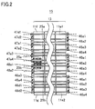
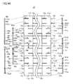
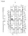
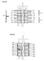
- Figs. 1 and 2 are plan views each illustrating a state where integrated wiring members 46, 47 and 48 are arranged at both ends of matrix 15 forming the solar cell module according to the present invention and both ends of a solar cell unit in matrix 15.
- Fig. 1 illustrates a state before connection of the solar cells through integrated wiring members 46, 47 and 48
- Fig. 2 illustrates a state after connection of the solar cells through integrated wiring members 46, 47 and 48.
- the matrix refers to a state of a group of the solar cells, wherein the plurality of solar cells 11 are arranged in line and are electrically connected to each other to thereby form a cell unit and a plurality of cell units formed as described above are arranged side by side.
- constituent members and constituent parts equal to those in the description of the conventional art are denoted by identical symbols.
- the plurality of solar cells 11 are arranged in line and are electrically connected to each other through wiring members 12 to form cell unit 13.
- connecting pieces 12 are connected to cell units 13 at both ends in a lateral direction, and connecting pieces 12c or 12b are led out.
- the plurality of cell units 13 (six in the examples illustrated in Figs.
- the present invention has a feature in the configurations of integrated wiring members 46, 47 and 48.
- Each of integrated wiring members 46, 47 and 48 is formed into a shape capable of connecting between the adjoining solar cells (11a1 and 11a2, 11b1 and 11b2, 11c1 and 11c2, 11d1 and 11d2, 11e1 and 11e2).
- the wiring member includes a part formed into an almost "I” shape and a part formed into an almost "F” shape in accordance with connection parts.
- the wiring member may be formed in accordance with a shape of a connection part.
- connection portions between integrated wiring members 46, 47 and 48 and connecting members 12 of the solar cell module are illustrated as bare portions 46al to 46a4 as for integrated wiring member 46, bare portions 47al to 47a4, 47dl and 47d2 as for integrated wiring member 47, and bare portions 48al to 48a4, 48dl and 48d2 as for integrated wiring member 48.
- integrated wiring members 47 and 48 are connected to electrical output extracting ports 25a and 25b at a center of one end of solar cell module 15.
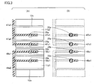
- Fig. 3 is an enlarged plan view mainly illustrating a connection state between an integrated wiring member and an electrical output extracting port.
- (A) is an enlarged view illustrating the solar cell in Fig. 2, when being seen from below
- (B) is also an enlarged view illustrating the solar cell in Fig. 2, when being seen from below. That is, Fig. 3 illustrates a module covered with a back cover as illustrated in Fig. 58.
- integrated wiring members 47 and 48 each having an almost "F" shape, two short axes orthogonal to a long axis are inserted into electrical output extracting ports 25a and 25b. Bare portions 47e1 and 47cl and bare portions 48el and 48c located at tip ends of these short axes are connected to wires (not illustrated) from the solar cell module.
- an integrated wiring member includes first integrated wiring member 47, second integrated wiring member 48 and third integrated wiring member 46 as illustrated in Fig. 1. Description will be given of these integrated wiring members with reference Figs. 4 to 8.
- first integrated wiring member 47 includes a first wiring member 47(I) and a second wiring member 47(II).
- First wiring member 47(I) includes a coupling piece 47d and a protruding piece 47e.
- Second wiring member 47(II) includes a coupling piece 47a and a protruding piece 47c.
- coupling piece 47a forms second wiring member 47(II), and laterally couples between connecting pieces 12c and 12b led out from the adjoining solar cells (11b1 and 11b2) located at a position above a center of a side edge of the solar cell provided with electrical output extracting ports 25a and 25b in Fig. 1.
- protruding piece 47c forms second wiring member 47(II), and is connected to a bypass diode (not illustrated in Fig. 1).
- coupling piece 47d forms first wiring member 47(I), and is coupled to connecting piece 12b led out from an electrode on a bottom face of solar cell 11f.
- Protruding piece 47e forms first wiring member 47(I), is mechanically coupled to electrical output extracting port 25a, and is electrically connected to an external terminal and a bypass diode.
- second wiring member 47(II) includes coupling piece 47a and protruding piece 47c, and is formed into an almost "L” shape.
- first wiring member 47(I) includes coupling 47d and protruding piece 47e, and is formed into an almost “L” shape.
- First wiring member 47(I) and second wiring member 47(II) are coated with a first coating member 471 and a second coating member 472, respectively.
- a portion to be connected to the connecting member from the solar cell is not coated with the coating member.
- first wiring member 47(I) and second wiring member 47(II) are integrated with each other through insulating and protecting films 50; thus, first integrated wiring member 47 is formed.
- second integrated wiring member 48 has a configuration similar to that of first integrated wiring member 47, and includes a first wiring member 48(I), a second wiring member 48(II) and insulating and protecting films 50 interposed between first wiring member 48(I) and second wiring member 48(II).
- First wiring member 48(I) includes a coupling piece 48d and a protruding piece 48e.
- Second wiring member 48(II) includes a coupling piece 48a and a protruding piece 48c.
- coupling piece 48a forms second wiring member 48(II), and laterally couples between connecting pieces 12b and 12c led out from the adjoining solar cells (11d1 and 11d2) located at a position below the center of the side edge of the solar cell in Fig. 1.
- Protruding piece 48c is connected to the bypass diode in Fig. 1.
- Coupling piece 48d is coupled to connecting piece 12c led out from an electrode on a top face of solar cell 11g.
- Protruding piece 48e is mechanically coupled to electrical output extracting port 25b, and is electrically connected to an external terminal and a bypass diode.
- second wiring member 48(II) includes coupling piece 48a and protruding piece 48c, and is formed into an almost "L” shape.
- first wiring member 48(I) includes coupling piece 48d and protruding piece 48e, and is formed into an almost "L” shape.
- First wiring member 48(I) and second wiring member 48(II) are coated with a coating member 481 and a coating member 482, respectively.
- a portion to be connected to the connecting member from the solar cell is not coated with the coating member.
- third integrated wiring member 46 includes a coupling piece 46a for laterally coupling between connecting pieces 12c and 12b led out from the adjoining solar cells (11a1 and 11a2, 11c1 and 11c2, 11e1 and 11e2) located at a side edge opposite to the side edge provided with electrical output extracting ports 25a and 25b in Fig. 1.
- Coupling piece 46a is coated with a coating member 461.
- Third integrated wiring member 46 only includes coupling piece 46a and coating member 461; however, this configuration is defined as third integrated wiring member 46 for the sake of convenience.
- three third integrated wiring members 46 among first, second and third integrated wiring members 46, 47 and 48 are required for connection between the solar cells. Therefore, there are required five integrated wiring members of three types as a whole.
- An electrical output extracting port 25 is provided with external terminals such as a diode external cable, and wiring members to be coupled to this electrical output extracting port are electrically connected to these terminals.
- the wiring member may be made of copper, CiC (copper/indium/copper), Ag, Au, Fe or the like.
- the wiring member has a solder-coated surface.
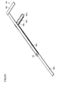
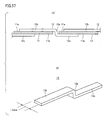
- Fig. 4 is a perspective view illustrating a state where first wiring member 47(I) and second wiring member 47(II) each forming first integrated wiring member 47 are disassembled from each other.
- first integrated wiring member 47 first integrated wiring member 47(I) and second wiring member 47(II) each forming first integrated wiring member 47 are disassembled from each other.
- first wiring member 47(I) includes coupling piece 47d for laterally connecting between connecting pieces 12b led out from the electrode on the bottom face of solar cell 11f and electrical output extracting port 25a of matrix 15, regions 47dl and 47d2 connected to two connecting pieces 12b led out from the electrode on the bottom face of solar cell 11f, and protruding piece 47e connected to an end, located opposite to regions 47dl and 47d2, of coupling piece 47d.
- coupling piece 47d may have a width of 6 mm and a thickness of 0.23 mm
- protruding piece 47e may have a width of 6 mm and a thickness of 0.23 mm.
- Coupling piece 47d and protruding piece 47e are connected by soldering to each other; thus, first wiring member 47(I) is formed into an almost "L" shape as a whole.
- first wiring member 47(I), formed as described above, is coated with insulative coating member 471 (diagonally shaded).
- end 47dl, located opposite to protruding piece 47e, of coupling piece 47d, a portion 47d2 close to a center relative to end 47dl, and tip end 47el of protruding piece 47e are bare portions with coating member 471 removed therefrom.
- bare portions 47dl and 47d2 are spaced away from each other by a predetermined distance.
- Bare portion 47dl and 47d2 are connected by soldering to the other connecting pieces 12b and 12b of connecting members 12 attached to solar cell 11f (see Fig. 1).
- Bare portion 47e1 is connected to a portion derived from electrical output extracting port 25a to the outside and a bypass diode (to be described later).
- the second wiring member 47(II) includes coupling member 47a, regions 47a1 and 47a2 connected to connecting pieces 12c led out from an electrode on a top face of solar cell 11b1, regions 47a3 and 47a4 connected to connecting pieces 12b led out from an electrode on a bottom face of solar cell 11b2, and protruding piece 47c connected to an end, located opposite to regions 47a1 and 47a2, of coupling piece 47a.
- each of coupling piece 47a and protruding piece 47c may have a width of 6 mm and a thickness of 0.23 mm.
- Coupling piece 47a and protruding piece 47c are connected by soldering to each other; thus, second wiring member 47(II) is formed into an almost "L" shape as a whole.
- coupling piece 47a and protruding piece 47c may be integrated with each other by punching or the like.
- Second wiring member 47(II), formed as described above, is entirely coated with insulative coating member 472 (diagonally shaded).
- end 47a1, located opposite to protruding piece 47c, of coupling piece 47a, portion 47a2 close to a center relative to end 47a1, portion 47a3 close to the center relative to portion 47a2, portion 47a4 close to the center relative to portion 47a3, and tip end 47c1 of protruding piece 47c are bare portions with coating member 472 removed therefrom.
- bare portions 47a1 and 47a2 are spaced away from each other by a predetermined distance.
- Bare portions 47a1 and 47a2 are connected by soldering to the other connecting pieces 12c and 12c of connecting members 12 attached to solar cell 11b1 (see Fig. 1). Bare portions 47a3 and 47a4 are spaced away from each other by a predetermined distance. Bare portions 47a3 and 47a4 are connected by soldering to the other connecting pieces 12b and 12b of connecting members 12 attached to solar cell 11b2 (see Fig. 1). Bare portion 47c1 is connected to a bypass diode (to be described later).
- each of coating members 471 and 472 may be used as each of coating members 471 and 472 for coating first wiring member 47(I) and second wiring member 47(II).
- each of coating members 471 and 472 is made of a material identical to that for the back film because a difference in degree of secular changes (bleaching) due to radiation of sunlight is not occurred, so that an aesthetic sense is not deteriorated.
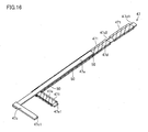
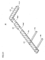
- Fig. 5 is a perspective view illustrating first integrated wiring member 47 in which first wiring member 47(I) and second wiring member 47(II), each illustrated in Fig. 4, are integrated with each other.
- Insulating and protecting films 50 with high heat-resistant property with respect to coating member 471 are arranged between bare portions 47a1, 47a2 and 47a3 each of which is connected to the solar cell and is not covered with coating member 472 and coupling piece 47d coated with coating member 471.
- insulating and protecting films 50 are inserted at positions illustrated in Fig. 4; thus, first wiring member 47(I) and second wiring member 47(II) can be integrated with each other before connection by soldering of each connection portion.
- examples of insulating and protecting film 50 may include a polyimide film, an aramid film, an SiPet film and the like.
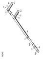
- Fig. 6 is a perspective view illustrating a state where first wiring member 48(I) and second wiring member 48(II), each forming second integrated wiring member 48, are disassembled from each other.
- an upper side illustrates second wiring member 48(II)
- a lower side illustrates first wiring member 48(I).
- second integrated wiring member 48 is a perspective view illustrating a state where first wiring member 48(I) and second wiring member 48(II), each forming second integrated wiring member 48, are disassembled from each other.
- an upper side illustrates second wiring member 48(II) and a lower side illustrates first wiring member 48(I).
- first wiring member 48(I) includes coupling piece 48d for laterally connecting between connecting pieces 12c led out from the electrode on the top face of solar cell 11g and electrical output extracting ports 25b of matrix 15, regions 48d1 and 48d2 connected to two connecting pieces 12c led out from the electrode on the upper face of solar cell 11g, and protruding piece 48e connected to an end, located opposite to regions 48d1 and 48d2, of coupling piece 48d.
- each of coupling piece 48d and protruding piece 48e may have a width of 6 mm and a thickness of 0.23 mm.
- Coupling piece 48d and protruding piece 48e are connected by soldering to each other; thus, first wiring member 48(I) is formed into an almost "L" shape as a whole. Then, first wiring member 48(I) is entirely coated with insulative coating member 481 (diagonally shaded). However, end 48d2, located opposite to protruding piece 48e, of coupling piece 48d, portion 48d1 close to a center relative to end 48d2, and tip end 48e1 of protruding piece 48e are bare portions with coating member 481 removed therefrom. Herein, bare portions 48d1 and 48d2 are spaced away from each other by a predetermined distance.
- Bare portions 48d1 and 48d2 are connected by soldering to the other connecting pieces 12c and 12c of connecting members 12 attached to solar cell 11g (see Fig. 1).
- Bare portion 48el is connected to a portion derived from electrical output extracting port 25b to the outside, and a bypass diode (to be described later).
- second wiring member 48(II) includes coupling piece 48a, regions 48a1 and 48a2 connected to connecting pieces 12c led out from an electrode on a top face of solar cell 11d1, regions 48a3 and 48a4 connected to connecting pieces 12b led out from an electrode on a bottom face of solar cell 11d2, and protruding piece 48c connected to an end, located opposite to regions 48a1 and 48a2, of coupling piece 48a.
- each of coupling piece 48a and protruding piece 48c may have a width of 6 mm and a thickness of 0.23 mm.
- Coupling piece 48a and protruding piece 48c are connected by soldering to each other; thus, second wiring member 48(II) is formed into an almost "L" shape as a whole.
- coupling piece 48a and protruding piece 48c may be integrated with each other by punching or the like.
- second wiring member 48(II) is entirely coated with insulative coating member 482 (diagonally shaded).
- end 48a4 located opposite to protruding piece 48c, of coupling piece 48a, portion 48a3 close to a center relative to end 48a4, portion 48a2 close to the center relative to portion 48a3, portion 48al close to the center relative to portion 48a2, and tip end 48cl of protruding piece 48c are bare portions with coating member 482 removed therefrom.
- bare portions 48al and 48a2 are spaced away from each other by a predetermined distance. Bare portions 48a1 and 48a2 are connected by soldering to the other connecting pieces 12c and 12c of connecting members 12 attached to solar cell 11d1 (see Fig. 1).
- Bare portions 48a3 and 48a4 are spaced away from each other by a predetermined distance. Bare portions 48a3 and 48a4 are connected by soldering to the other connecting pieces 12b and 12b of connecting members 12 attached to solar cell 11d2 (see Fig. 1). Bare portion 48cl is connected to a bypass diode (to be described later).
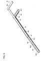
- Fig. 7 is a perspective view illustrating second integrated wiring member 48 in which first wiring member 48(I) and second wiring member 48(II), each illustrated in Fig. 6, are integrated with each other.
- Insulating and protecting films 50 with high heat-resistant property with respect to coating member 481 are arranged between bare regions 48a1, 48a2 and 48a3, each of which is connected to the solar cell and is not coated with coating member 482, and coupling piece 48d coated with coating member 481.
- insulating and protecting films 50 are inserted at positions illustrated in Fig. 8; thus, first wiring member 48(I) and second wiring member 48(II) can be integrated with each other before connection by soldering of each connection portion.
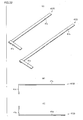
- Fig. 8 is a perspective view illustrating third integrated wiring member 46.
- third integrated wiring member 46 is a perspective view illustrating third integrated wiring member 46.
- third wiring member 46 includes coupling piece 46a, regions 46a1 and 46a2 connected to connecting pieces 12c led out from an electrode on a top face of each of solar cells 11a1, 11c1 and 11e1, and regions 46a3 and 46a4 connected to connecting pieces 12b led out from an electrode on a bottom face of each of solar cells 11a2, 11c2 and 11e2.
- Third wiring member 46 is formed into an almost "I" shape.
- coupling piece 46a may have a width of 6 mm and a thickness of 0.23 mm.
- third integrated wiring member 46 formed as described above, is entirely coated with insulative coating member 461 (diagonally shaded).
- end 46a1 of coupling piece 46a and portion 46a2 close to a center relative to end 46a1 are spaced away from each other by a predetermined distance, and are bare portions with coating member 461 removed therefrom.
- Bare portions 46a1 and 46a2 are connected by soldering to the other connecting pieces 12c and 12c of connecting members 12 attached to each of solar cells 11a1, 11c1 and 11e1 (see Fig. 1).
- end 46a4 of coupling piece 46a and portion 46a3 close to the center relative to end 46a4 are spaced away from each other by a predetermined distance, and are bare portions with coating member 461 removed therefrom. Bare portions 46a3 and 46a4 are connected by soldering to the other connecting pieces 12b and 12b of connecting members 12 attached to each of solar cells 11a2, 11c2 and 11e2 (see Fig. 1).
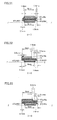
- Fig. 9 illustrates examples of sectional structures of first, second and third integrated wiring members 46, 47 and 48.
- FIG. 9 (A), (B), (C), (D), (E) and (F) are sectional views taken along broken lines A-A, B-B, C-C, D-D, E-E and F-F in Figs. 5, 7 and 8, respectively.
- A) to (F) of Fig. 9 dimensions of the respective components are described as examples. However, the present invention does not intend to be interpreted by limitation of these dimensions.
- first integrated wiring member 47 in addition to a coating method of a coating member with reference to Figs. 4, 5 and 9.
- coupling piece 47a is coated with coating member 472
- coupling piece 47d is coated with coating member 471.
- a copper-wire formed body obtained in such a manner that solder-plated copper wires having widths of 6 mm and 1.5 mm and a thickness of 0.23 mm are connected by soldering to each other so as to integrally form an almost "L" shape is covered with a film as coating member 472 with insulation performance and selectable color such as a PET film.
- an adhesive, a double-faced tape or the like may be used.
- one insulating film 472 is folded in two, and the copper-wire formed body is sandwiched therebetween.
- one insulating film 472 is folded in two as described above, a deviation of the copper-wire formed body is suppressed upon adhesion, so that insulation performance can be ensured with reliability.
- the copper-wire formed body is covered with EVA resin upon manufacturing of a solar cell module in a subsequent step. Therefore, completed first integrated wiring member 47 must be previously subjected to vacuum lamination or deaeration in order to prevent generation of air bubbles in the EVA resin.
- an adhesive or a double-faced tape which does not exert an adverse influence on the EVA resin must be selected herein.
- the tip end of coating member 472 for coating protruding piece 47c of second wiring member 47(II) has tapered face P cut obliquely.
- Tapered face P exhibits the following advantage. That is, when bare portion 47c1 of second wiring member 47(II) is derived from electrical output extracting port 25a formed in back cover 17 made of a conductive film to the outside, the tip end (tapered face P) of coating member 472 can smoothly pass through electrical output extracting port 25a without catch in peripheral portions of electrical output extracting port 25a.
- first integrated wiring member 47 as the copper-wire formed body wherein second wiring member 47(II) having coupling piece 47a and protruding piece 47c connected therebetween is coated with coating member 472.
- first wiring member 47(I) as the copper-wire formed body wherein solder-plated copper wires having widths of 6 mm and 1.5 mm and a thickness of 0.23 mm are connected by soldering to each other so as to have an almost "L" shape and, then, are coated with coating member 471.
- first wiring member 47(I) and second wiring member 47(II) are used for fixing first wiring member 47(I) and second wiring member 47(II) at respective desired positions so as to integrate first wiring member 47(I) with second wiring member 47(II); thus, first integrated wiring member 47 is completed.
- insulating and protecting film 50 is interposed between first wiring member 47(I) and second wiring member 47(II).
- a broken line Z-Z is a reference line indicating a positional relation of each section.
- Each of broken lines Z-Z described subsequently in the present specification has similar meaning.
- FIG. 9 illustrates a sectional structure taken along a broken line A-A in Fig. 5.
- coupling piece 47d which is a solder-plated flat copper wire having a width of 6 mm, is bared.
- first wiring member 47(I) other than the face, where connection by soldering is performed is coated with coating member 471.
- FIG. 9 illustrates a sectional structure taken along a broken line B-B in Fig. 5.
- coupling piece 47d which is a solder-plated flat copper wire having a width of 6 mm
- film-shaped coating member 471 folded in two as described above.
- a distance between an outer tip end on the folded side of coating member 471 and the tip end of coupling piece 47d in an identical direction is 0.1 mm
- a distance between an apex of overlaid both ends of folded coating member 471 and the tip end of coupling piece 47d in an identical direction is 1.9 mm.
- coating member 471 has an outer dimension of about 0.2 mm to 0.3 mm in a thickness direction.
- FIG. 9 illustrates a sectional structure taken along a broken line C-C in Fig. 6.
- insulating and protecting film 50 with high heat-resistant property with respect to coating member 471 is placed immediately on first wiring member 47(I) coated with film-shaped coating member 471 folded in two, and a portion, which is not coated with film-shaped coating member 472, of second wiring member 47(II) is placed immediately on insulating and protecting film 50.
- a distance between an outer tip end on the folded side of coating member 471 and the tip end of insulating and protecting film 50 in an identical direction is 0.5 mm
- a distance between the tip end of insulating and protecting film 50 and the tip end of coupling piece 47a of second wiring member 47(II) in an identical direction is 0.5 mm
- a distance between an apex of overlaid both ends of coating member 471 and the tip end of insulating and protecting film 50 in an identical direction is 0.5 mm
- a distance between the tip end of insulating and protecting film 50 and the tip end of coupling piece 47a of second wiring member 47(II) in an identical direction is 1.0 mm.
- Coupling piece 47a of first wiring member 47(I) and coupling piece 47d of second wiring member 47(II) are 6.0 mm in width, and are displaced from each other by 0.4 mm. That is, when being seen from the light receiving face of the solar cell module (when being seen from below in Fig. 9), insulating and protecting film 50 is shielded by coating member 471, and coupling piece 47a of first wiring member 47(I) is located inward with respect to the width of insulating and protecting film 50.
- the numerical values described herein are merely examples, and the present invention is not limited thereto as long as the aforementioned states are kept. Thus, if insulating and protecting film 50 with high heat-resistant property is different in color from coating member 471 and back cover 17, the aforementioned feature is effectively exerted; thus, an aesthetic sense of the surface of the solar cell module can be maintained.
- FIG. 9 illustrates a sectional structure taken along a broken line D-D in Fig. 5.
- second wiring member 47(II) coated with film-shaped coating member 472 folded in two is placed immediately on first wiring member 47(I) coated with film-shaped coating member 471 folded in two.
- coupling piece 47d of first wiring member 47(I) and coupling piece 47a of second wiring member 47(II) are 6.0 mm in width and are displaced from each other by 0.4 mm.
- FIG. 9 illustrates a sectional structure taken along a broken line E-E in Fig. 5.
- coupling piece 47a which is a solder-plated flat copper wire having a width of 6 mm
- film-shaped coating member 472 folded in two A distance between an outer tip end of the folded side of coating member 472 and the tip end of coupling piece 47a in an identical direction is 0.1 mm, and a distance between an apex of overlaid both ends of coating member 472 and the tip end of coupling piece 47a in an identical direction is 1.9 mm.
- coating member 472 has an outer dimension of about 0.2 mm to 0.3 mm in a thickness direction.
- FIG. 9 illustrates a sectional structure taken along a broken line F-F in Fig. 5.
- coupling piece 47a which is a solder-plated flat copper wire having a width of 6 mm, is bared.
- Coupling member 47a other than the face, where connection by soldering is performed, may be coated with coating member 472.
- the first integrated wiring member is a combination of wiring members for a solar cell module, and includes (i) a part configured by a first wiring member, (ii) a part configured by the first wiring member coated with a first coating member, (iii) a part configured by a second wiring member adjoining to the first wiring member coated with the first coating member via an insulating and protecting film, (iv) a part configured by the second wiring member which adjoins to the first wiring member coated with the first coating member and is coated with a second coating member, (v) a part configured by the second wiring member coated with the second coating member, and (vi) a part configured by the second wiring member.
- first integrated wiring member 47 The aforementioned description is given of the sectional structure of first integrated wiring member 47. It is needless to say that the same holds true for second integrated wiring member 48 and third integrated wiring members 46. In particular, those skilled in the art readily understand that second integrated wiring member 48 and first integrated wiring member 47 are related in structure as mirror image and have a similar structure.
- first, second and third integrated wiring members 46, 47 and 48 are mainly connected by soldering to solar cells. Therefore, insulating and protecting film 50 excellent in heat-resistant property is used herein. Use of insulating and protecting film 50 leads to improved aesthetic sense because of widened choice of coating member 472
- a wiring step for a solar cell module using first, second and third wiring members 46, 47 and 48 with reference to Figs. 1 and 2.
- three third integrated wiring members 46, 46 and 46 are arranged along the adjoining solar cells (11a1 and 11a2, 11c1 and 11c2, 11e1 and 11e2) located at the side edge of matrix 15, respectively (see Fig. 1).
- bare portions 46a1 and 46a2 of uppermost third integrated wiring member 46 in Fig. 1 are connected by soldering to the other connecting pieces 12c and 12c of connecting members 12 attached to solar cell 11a1 with the use of a soldering iron or the like.
- bare portions 46a3 and 46a4 of uppermost third wiring member 46 are connected by soldering to the other connecting pieces 12b and 12b of connecting members 12 attached to solar cell 11 a2 with the use of a soldering iron or the like.
- bare portions 46al and 46a2 of middle third integrated wiring member 46 in Fig. 1 are connected by soldering to the other connecting pieces 12c and 12c of connecting members 12 attached to solar cell 11c1 with the use of a soldering iron or the like.
- bare portions 46a3 and 46a4 of middle third integrated wiring member 46 are connected by soldering to the other connecting pieces 12b and 12b of connecting members 12 attached to solar cell 11c2 with the use of a soldering iron or the like.
- bare portions 46al and 46a2 of lowermost third integrated wiring member 46 in Fig. 1 are connected by soldering to the other connecting pieces 12c and 12c of connecting members 12 attached to solar cell 11e1 with the use of a soldering iron or the like.
- bare portions 46a3 and 46a4 of lowermost third integrated wiring member 46 are connected by soldering to the other connecting pieces 12b and 12b of connecting members 12 attached to solar cell 11e2 with the use of a soldering iron or the like.
- first integrated wiring member 47 is arranged along the adjoining solar cells (11b1 and 11b2) located at a position above a center of the edge of matrix 15 (see Fig. 1).
- bare portions 47al and 47a2 of second wiring member 47(II) are connected by soldering to the other connecting pieces 12c and 12c of connecting members 12 attached to solar cell 11b1 with the use of a soldering iron or the like.
- bare portions 47a3 and 47a4 of second wiring member 47(II) are connected by soldering to the other connecting pieces 12b and 12b of connecting members 12 attached to solar cell 1 1b2 with the use of a soldering iron or the like.
- first wiring member 47(I) bare portions 47d1 and 47d2 of first wiring member 47(I) are connected by soldering to the other connecting pieces 12b and 12b of connecting members 12 attached to solar cell 11f with the use of a soldering iron or the like.
- tip end 47e1 of protruding piece 47e of first wiring member (I) is derived from electrical output extracting port 25a to the outside.
- a bypass diode (not illustrated) is connected between tip end 47c1 of protruding piece 47c of second wiring member 47(II) and tip end 47e1 of protruding 47e of first wiring member 47(I).
- second integrated wiring member 48 is arranged along the adjoining solar cells (11d1 and 11d2) located at a position below the center of the edge of matrix 15 (see Fig. 1).
- bare portions 48a1 and 48a2 of second wiring member 48(II) are connected by soldering to the other connecting pieces 12c and 12c of connecting members 12 attached to solar cell 11d1 with the use of a soldering iron or the like.
- bare portions 42a3 and 42a4 of second wiring member 48(II) are connected by soldering to the other connecting pieces 12b and 12b of connecting members 12 attached to solar cell 11d2 with the use of a soldering iron or the like.
- bare portions 48d1 and 48d2 of first wiring member 48(I) are connected by soldering to the other connecting pieces 12c and 12c of connecting members 12 attached to solar cell 11g with the use of a soldering iron.
- tip end 48e1 of protruding piece 48e of first wiring member 48(I) is derived from electrical output extracting ports 25b to the outside.
- a bypass diode (not illustrated) is connected between tip end 48c1 of protruding piece 48c of second wiring member 48(II) and tip end 48e1 of protruding piece 48e of first wiring member 48(I).
- soldering operations may be performed successively as described above or may be performed at a time.
- the soldering operations are not in particular order.
- Fig. 2 illustrates a state after completion of the wiring work.
- connecting pieces 12b, 12b, 12c, 12c, ... protruding from the side edges of matrix 15 are cut (shown by broken lines in Fig. 2) after completion of the wiring work.
- Fig. 3 is an enlarged view mainly illustrating a connection state between integrated wiring members 47 and 48 and the electrical output extracting ports in the solar cell.
- (A) is a plan view when being seen from the bottom face side of the solar cell module and (B) is also a plan view when being seen from the bottom face side of the solar cell module.
- the solar cell module is formed while being covered with the back cover as illustrated in Fig. 58.
- Fig. 3 illustrates a positional relation of the wiring members near electrical output extracting ports 25a and 25b.
- Protruding pieces 47c1 and 47e1 connected to electrical output extracting ports 25a and protruding pieces 48c1 and 48e1 connected to electrical output extracting ports 25b are connected to external terminals, respectively.
- first, second and third integrated wiring members 46, 47 and 48 formed in accordance with this embodiment when first, second and third integrated wiring members 46, 47 and 48 formed in accordance with this embodiment are used, 24 soldered connection parts are aligned orderly.
- work for connection by soldering can be simplified, a time for this work can be reduced, and efficiency for this work can be significantly improved.
- each of first, second and third integrated wiring members 46, 47 and 48 is coated with a member excellent in insulation performance and moisture-resistant performance such as a PET film. Therefore, even if generation of air bubbles or separation is occurred at the silicone resin, the EVA resin or the like, protection by coating members 461, 471 and 481 makes it possible to significantly reduce a possibility of generation of insulation failure.
- first, second and third integrated wiring members 46, 47 and 48 are coated with coating members 461, 471 and 481 exhibits the following advantage in comparison with a conventional case in terms of outer appearance. That is, soldered portions (47a1, 47a2, 47a3, 48a1, 48a2, 48a3) in second wiring members 47(II) and 48(II) are shielded from the top face side of the solar cell module by coating members 471 and 481 for coating coupling pieces 47d and 48b of first wiring members 47(I) and 48(I) each extracting an electrical output from the ends of matrix 15 configured by the solar cells connected in series.
- an aesthetic sense can be ensured even when the solar cell module is seen from a position under the eaves.
- first, second and third integrated wiring members 46, 47 and 48 are coated with the coating members except portions to be connected by soldering to connecting pieces 12b and connecting pieces 12c of connecting members 12 attached to the solar cells.
- protruding pieces 47c and 48c of second wiring members 47(II) and 48(II) and protruding pieces 47e and 48e of first wiring members 47(I) and 48(I) are partly located at the bottom face side of the solar cell module after completion of the connection by soldering.
- the hidden portions are not seen from the top face side of the solar cell module and, therefore, may not be coated with coating members.
- the respective coupling pieces of first, second and third integrated wiring members 46, 47 and 48 which are inconspicuous when being seen from the top face side of the solar cell module, may not be coated with coating members partly.
- the first wiring member and the second wiring member are independently coated with coating members; thus, an insulating property can be retained. Further, film-shaped insulating and protecting films with high heat-resistant property can be arranged only at desired positions; thus, cost reduction can be achieved.
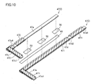
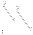
- Fig. 10 is a perspective view illustrating first wiring member 47(I) and second wiring member 47(II) separated from each other in first integrated wiring member 47.
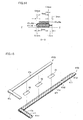
- Fig. 11 is a perspective view illustrating first integrated wiring member 47 in which first wiring member 47(I) and second wiring member 47(II) separated from each other in Fig. 10 are integrated with each other.
- Fig. 12 is a perspective view illustrating first wiring member 48(I) and second wiring member 48(II) separated from each other in second integrated wiring member 48.
- Fig. 13 is a perspective view illustrating second integrated wiring member 48 in which first wiring member 48(I) and second wiring member 48(II) separated from each other in Fig. 12 are integrated with each other.
- Embodiment 2 is similar to Embodiment 1 except that there are omitted coating members 472 and 482 on portions of first wiring members 47(I) and 48(I) shielded from the top face side of the solar cell module by first coating members 471 and 481 on first wiring members 47(I) and 48(I). More specifically, as illustrated in Figs. 10 and 12, coupling pieces 47a and 48a of second wiring members 47(II) and 48(II), which are substantially overlaid on portions extending from bare portions 47d2 and 48d2 of coupling pieces 47d and 48d to protruding pieces 47e and 48e in first wiring members 47(I) and 48(I), are not partly coated with coating members 472 and 482. That is, coupling pieces 47a and 48a are partly bared.
- first wiring members 47(I) and 48(I) are integrated with second wiring members 47(II) and 48(II), respectively, the bare portions in second wiring members 47(II) and 48(II) are shielded from sunlight by the portions, substantially overlaid on second wiring members 47(II) and 48(II), respectively, of first wiring members 47(I) and 48(I).
- the bare portions may not be coated with the coating member.
- insulating and protecting films 50 ensure an insulation property between first wiring members 47(I) and 48(I) and second wiring members 47(II) and 48(II)
- the bare portions may not be coated with the coating members.
- an amount of coating members for the second wiring member is reduced, which is economically advantageous.
- a time for a coating process can be reduced, which is preferable.
- Fig. 14 is a sectional view taken along a broken line D-D in each of Figs. 11 and 13.
- second wiring members 47(II) and 48(II) are placed immediately on first wiring members 47(I) and 48(I) coated with film-shaped coating members 471 and 481 each folded in two.
- an adhesive tape 60 or the like is used upon integration of first wiring members 47(I) and 48(I) with second wiring members 47(II) and 48(II).
- Adhesive tape 60 may be made of a material of a thermoplastic film (ACF: Anisotropic Conductive Film).
- the adhesive tape has a width almost equal to that of insulating and protecting film 50.
- the first integrated wiring member is a combination of wiring members for a solar cell module, and includes (i) a part configured by a first wiring member, (ii) a part configured by the first wiring member coated with a first coating member, (iii) a part configured by a second wiring member adjoining to the first wiring member coated with the first coating member via an insulating and protecting film, (iv) a part configured by the second wiring member adjoining to the first wiring member coated with the first coating member, (v) a part configured by the second wiring member coated with the second coating member, and (vi) a part configured by the second wiring member.
- first integrated wiring member 47 The aforementioned description is given of the sectional structure of first integrated wiring member 47. It is needless to say that the same holds true for second integrated wiring member 48 and third integrated wiring member 46. In particular, those skilled in the art readily understand that second integrated wiring member 48 and first integrated wiring member 47 are related in structure as mirror image and have a similar structure.
- Fig. 15 is a perspective view illustrating first wiring member 47(I) and second wiring member 47(II) separated from each other in first integrated wiring member 47.
- second wiring member 47(II) is coated with no coating member.
- Fig. 16 is a perspective view illustrating first integrated wiring member 47 in which first wiring member 47(I) and second wiring member 47(II) separated from each other in Fig. 15 are integrated with each other.
- Fig. 17 is a perspective view illustrating a state where the first integrated wiring member in Fig. 16 is coated with the coating member.
- Fig. 18 is a perspective view illustrating first wiring member 48(I) and second wiring member 48(II) separated from each other in second integrated wiring member 48.
- second wiring member 48(II) is coated with no coating member.
- Fig. 19 is a perspective view illustrating second integrated wiring member 48 in which first wiring member 48(I) and second wiring member 48(II) separated from each other in Fig. 18 are integrated with each other.
- Fig. 20 is a perspective view illustrating a state where the second integrated wiring member in Fig. 19 is coated with the coating member.
- second wiring members 47(II) and 48(II) are not coated with coating members 472 and 482. That is, the first wiring member is coated with no coating member.
- second wiring members 47(II) and 48(II) coated with no coating members are integrated with first wiring members 47(I) and 48(I).
- the first wiring members and the second wiring members are collectively and fixedly coated with film-shaped third coating members 473 and 483 each folded in two.
- the second wiring member coated with no coating member is integrated with the first wiring member.
- the second wiring member and the first wiring member are collectively coated with the coating member.
- the integrated wiring member according to this embodiment requires only one positional adjustment.
- the long wiring member (the first wiring member in this embodiment) is fixed to only the connecting piece of connecting member 12 attached to the endmost solar cell and, therefore, becomes an unstable state upon manufacturing of a solar cell module.
- a tape for fixing the wiring member is required.
- the integration in this embodiment makes it possible to entirely fix parallel members to the connecting pieces of connecting members 12 attached to the solar cell.
- this embodiment exhibits an advantageous effect that there are no tape and work for fixing wiring members independently.
- insulating and protecting films 50 are interposed between portions serving as bare portions in second wiring members 47(II) and 48(II) and first wiring members 47(I) and 48(I).
- the reason therefor is as follows: the first wiring member and the second wiring member are prevented from contact with each other, that is, are insulated from each other.
- Embodiment 3 is similar to Embodiment 1 except that the first wiring member is integrated with the second wiring member in a state where the first wiring member is coated with no coating member and, then, the first wiring member and the second wiring member are coated with the coating member.
- Fig. 21 illustrates a sectional structure of the integrated wiring member taken along a broken line D-D in each of Figs. 17 and 20.
- second wiring members 47(II) and 48(II) coated with no coating members are integrated with first wiring members 47(I) and 48(I) and, then, the first wiring member and the second wiring member are integrally coated with the coating member, as illustrated in Fig. 21, second wiring members 47(II) and 48(II) are placed immediately on first wiring members 47(I) and 48(I) coated with film-shaped coating members 471 folded in two and, then, the first wiring member and the second wiring member are coated with film-shaped coating member 473 folded in two.
- the first integrated wiring member is a combination of wiring members for a solar cell module, and includes (i) a part configured by a first wiring member, (ii) a part configured by the first wiring member coated with a first coating member, (iii) a part configured by a second wiring member adjoining to the first wiring member coated with the first coating member via an insulating and protecting film, (iv) a part where the first wiring member coated with the first coating member and the second wiring member adjoining thereto are coated with a third coating member, (v) a part configured by the second wiring member coated with the second coating member, and (vi) a part configured by the second wiring member.
- the first wiring member and the second wiring member which is coated with no coating member are laminated with and fixed to each other by one coating member; thus, a coating step can be simplified and cost reduction can be achieved.
- FIG. 22 is a perspective view illustrating a state where first integrated wiring member 47 is divided into first wiring member 47(I) and second wiring member 47(II). As illustrated in (A) of Fig. 22, first and second wiring members 47(I) and 47(II) are not coated with the coating members, respectively.
- FIG. 22 is a plan view of first wiring member 47(I) illustrated in (A) of Fig. 22, when being seen from above, that is, a plan view of first wiring member 47(I) when being seen from the bottom face side of the solar cell module.
- (C) is a plan view of first wiring member 47(I) illustrated in (A) of Fig. 22, when being seen from below, that is, a plan view of first wiring member 47(I) when being seen from the light receiving face side of the solar cell module. Also in the following drawings, a relation between the top face and the bottom face of the solar cell module is invariant.
- first wiring member 47(I) includes coupling piece 47d and protruding piece 47e each having, for example, a width of 6 mm and a thickness of 0.2 mm
- second wiring member 47(II) includes coupling piece 47a and protruding piece 47c each having, for example, a width of 6 mm and a thickness of 0.2 mm.
- first and second wiring members 47(I) and 47(II) are not coated with the coating members.
- protruding piece 47e of first wiring member 47(I) is entirely coated with coating member 471 except the tip end thereof. Bare portion 47e1, which is the tip end of protruding piece 47e, is thus formed.
- coating member 471 folded in two is made contact with protruding piece 47e of the almost "L"-shaped wiring member and, then, is aligned with one of edges.
- coating member 471 is made contact with and aligned with protruding member 47e in such a manner that the outer side, that is, the left side face of the almost "L"-shaped wiring member illustrated in (B) and (C) of Fig.
- a full width at maximum of coating member 471 is designed as a width of a margin based on a width of protruding piece 47e. For example, when protruding piece 47e has a width of 6 mm and a thickness of 0.2 mm, the full width at half maximum is obtained from the following expression: (6.2 mm + margin) x 2 + 0.2 mm.
- FIG. 23 (B) and (C) are plan views of the first wiring member illustrated in (A) when being viewed from above and below, respectively.
- insulating and protecting film 50 wider in width than coupling piece 47d of first wiring member 47(I) is stuck to a part of coupling piece 47d by an adhesive or the like.
- insulating and protecting film 50 preferably has a width of 6.2 mm or more. In this embodiment, for example, insulating and protecting film 50 may have a width of 9 mm.
- insulating and protecting film 50 is stuck to coupling piece 47d so as to protrude from coupling piece 47d by about 2 mm in a direction opposite to a direction that protruding piece 47e protrudes. That is, insulating and protecting film 50 protrudes from coupling piece 47d by about 1 mm in the direction that protruding piece 47e protrudes. In order to ensure insulation with reliability, preferably, insulating and protecting film 50 protrudes from a corner of the "L" shape formed by protruding piece 47e and coupling piece 47d (side face of protruding piece 47e or tip end face of coupling piece 47d) by about 1 mm.
- insulating and protecting film 50 is wound around coupling piece 47d in second wiring member 47(I) in the direction opposite to protruding piece 47e in first wiring member 47(I). Then, as illustrated in (A) of Fig. 25, second wiring member 47(II) is stuck to the surface of insulating and protecting film 50 stuck to coupling piece 47d.
- (B) and (C) illustrate states of (A) when being seen from above and below, respectively.
- insulating and protecting film 50 protrudes from coupling piece 47d by about 1 mm in width in the direction that protruding piece 47e protrudes.
- protruding piece 47c is entirely coated with coating member 472 except tip end 47c1 of protruding piece 47c of second wiring member 47(II).
- the tip end of protruding piece 47c serves as bare portion 47c1.
- coating member 472 folded in two is made contact with protruding piece 47c of the almost "L"-shaped wiring member and, then, is aligned with one of edges.
- coating member 472 is made contact with and aligned with protruding member 47c in such a manner that the outer side, that is, the left side face of the almost “L"-shaped wiring member illustrated in (B) and (C) of Fig. 26 is fit to the valley portion of folded coating member 472.
- a positional reference between the coating member and the wiring member can be readily determined, resulting in improved workability.
- FIG. 26 (B) and (C) are plan views of the first and second wiring members, coated with coating member 473, illustrated in (A) when being viewed from above and below, respectively.
- first wiring member 47(I), insulating and protecting film 50 and second wiring member 47(II) are collectively integrated with each other as illustrated in (A) of Fig. 26 in such a manner that coating member 473 (473a, 473b, 473c) is folded in two along a broken line and, then, first wiring member 47(I) and second wiring member 47(II) are coated with coating member 473.
- coating member 473 is formed so as to be opened only at portions 47a1, 47a2 and 47a3 to be connected by soldering to wires 12 which will be led out from the cell.
- a face opposite to the soldered connection portion that is, a portion of first wiring member 47(I) corresponding to the opening of second wiring member 47(II) is coated with the third coating member (see (B) and (C) of Fig. 26). That is, as illustrated in (C) of Fig. 27, a region from the light receiving face of the solar cell module to first wiring member 47(I) is coated with and shielded by the coating member.
- portion 47a4 to be connected by soldering to wire 12, which will be led out from the cell is formed between coating members 473b and 473a.
- portion 47d2 to be connected by soldering to wire 12, which will be led out from the cell, is formed between coating members 473a and 473c.
- the first wiring member 47(I) is coated with coating member 473c so as to form bare portion 47d1 corresponding to the tip end of protruding piece 47d.
- Fig. 28 is a sectional view illustrating a sectional structure taken along a broken line C-C in each of (A) to (C) of Fig. 27.
- coupling piece 47d of first wiring member 47(I) is coated with film-shaped insulating and protecting film 50 with high heat-resistant property, which is folded in two, and coupling piece 47a of second wiring member 47(II) is placed immediately on insulating and protecting film 50. Further, coupling piece 47d of first wiring member 47(I), insulating and protecting film 50, and coupling piece 47a of second wiring member 47(I) are collectively coated with film-shaped coating member 473 folded in two.
- a distance between the outer tip end on the folded side of coating member 473 and the bare portion of coupling piece 47a of second wiring member 47(II) is 0.5 mm.
- a distance between the tip end, opposite to the folded side, of coating member 473 and the tip end of insulating and protecting film 50 in an identical direction is 0.5 mm.
- a distance between the tip end of insulating and protecting film 50 and the tip end of coupling piece 47d of first wiring member 47(I) in an identical direction is 1.4 mm.
- each of coupling piece 47d of first wiring member 47(I) and coupling piece 47a of second wiring member 47(II) has a width of 6 mm, and the end face on the folded side of insulating and protecting film 50 is overlaid on the tip end of coupling piece 47d of first wiring member 47(I) in an identical direction in a state where the end face on the folded side of insulating and protecting film 50 is flush with the tip end of coupling piece 47d of first wiring member 47(I). Therefore, coupling piece 47d of first wiring member 47(I) is displaced from coupling piece 47a of second wiring member 47(II) by the thickness of insulating and protecting film 50.
- insulating and protecting film 50 When being seen from the light receiving face side of the solar cell module (when being seen from below in Fig. 28), insulating and protecting film 50 is shielded by coating member 473, that is, coupling piece 47a of second wiring member 47(II) is located inward with respect to the width of insulating and protecting film 50.
- the numerical values described herein are merely examples, and the present invention is not limited thereto as long as the aforementioned states are kept. Thus, if insulating and protecting film 50 with high heat-resistant property is different in color from coating member 471 and back cover 17, the aforementioned feature is effectively exerted; thus, an aesthetic sense of the surface of the solar cell module can be maintained.
- Fig. 29 is a sectional view illustrating a sectional structure taken along a broken line D-D in each of (A) to (C) of Fig. 27.
- the structure illustrated in Fig. 29 is similar to that illustrated in Fig. 28 except that there is no bare portion of coupling piece 47a of second wiring member 47(II).
- coupling piece 47d of first wiring member 47(I), insulating and protecting film 50, and coupling piece 47a of second wiring member 47(II) can be integrated with and fixed to each other in such a manner that these components are coated with coating member 473 folded in two.
- Film-shaped insulating and protecting film 50 with high heat-resistant property is folded back along first wiring member 47(I), so that a creepage distance between first wiring member 47(I) and second wiring member 47(II) can be ensured; thus, an insulation property can be improved.
- Figs. 30 and 31 are sectional views each illustrating a case where insulating and protecting film 50 is not folded back along coupling piece 47d of first wiring member 47(I) in Figs. 28 and 29.
- the structures illustrated in Figs. 30 and 31 are similar to those illustrated in Figs. 28 and 29 except that the end of coupling piece 47d of first wiring member 47(I) and coupling piece 47a of second wiring member 47(II) are placed while being evenly spaced away from the end of insulating and protecting film 50 by, for example, 1.4 mm.
- the end of film-shaped insulating and protecting film 50 with high heat-resistant property is coated while being spaced away from the ends of first and second wiring members 47(I) and 47(II) by a certain distance, so that a creepage distance between first wiring member 47(I) and second wiring member 47(II) can be ensured; thus, an insulation property can be improved.
- Figs. 32 and 33 are sectional views each illustrating a case where insulating and protecting film 50 is not folded back along coupling piece 47d of second wiring member 47(II) in Figs. 28 and 29.
- the structures illustrated in Figs. 32 and 33 are similar to those illustrated in Figs.
- one of the ends of insulating and protecting film 50 is overlaid on the tip end of coupling piece 47a of second wiring member 47(II) in such a manner that one of the ends of insulating and protecting film 50 is flush with the tip end of coupling piece 47a of second wiring member 47(II), so that a creepage distance between first wiring member 47(I) and second wiring member 47(II) on the end face side to be connected to the connecting pieces of connecting members 12 can be ensured; thus, an insulation property can be improved.
- the portion, which is not connected to the connecting piece of connecting member 12, can be brought into no contact with (can be insulated from) the outside as much as possible.
- the top face of the solar cell module is coated with a film (insulating film) having a color identical to that of the back film; therefore, an aesthetic sense can be improved.
- Figs. 34 and 35 illustrate a relative positional relation between coating member 473 of first integrated wiring member 47 and the solar cell.
- Cells 11f, 11b1 and 11b2 each having a size of 155 mm-square are arranged at a space of 3 mm.
- Connecting pieces 12b or 12c attached to cells 11f, 11b1 and 11b2 are connected to first integrated wiring member 47; however, the connection portions are determined by openings of coating member 473.
- the cell unit including cell 11f, the cell unit including cell 11b1 and the cell unit including cell 11b2 are manufactured in accordance with single specifications; therefore, a pitch between connecting pieces 12b is equal to a pitch between connecting pieces 12c.
- such a pitch may be set at 77 mm.
- a pitch between connecting piece 12b and connecting piece 12c in the adjoining cell units is 81 mm including a space between cell units of 3 mm. If the opening of coating member 473, which is the connection portion of connecting pieces 12b and 12c, must have a thickness of 10 mm, a layout illustrated in Fig. 34 is required. As an alternative embodiment of Fig. 34, as illustrated in Fig.
- openings of coating member 473 that is, openings each having a width of 10 mm and openings each having a width of 14 mm are prepared so as to achieve a symmetrical form, so that coating member 473 for first integrated wiring member 47 can be used for second integrated wiring member 48, leading to preferable results that manufacturing cost can be reduced and manufacturing efficiency can be enhanced.
- the first integrated wiring member is a combination of wiring members for a solar cell module, and includes (i) a part configured by a first wiring member, (ii) a part configured by a third coating member coated with the first coating member, (iii) a part where a second wiring member adjoining to the first wiring member via an insulating and protecting film is at least partly coated with the third coating member, (iv) a part where the second member adjoining to the first wiring member via the insulating and protecting film is coated with the third coating member, (v) a part configured by the second coating member coated with the third coating member, (vi) a part coated with the second coating member, (vii) a part configured by the second wiring member coated with the second coating member, and (viii) a part configured by the first wiring member coated with the first coating member.
- first integrated wiring member 47 As an example. Since second integrated wiring member 48 and first integrated wiring member 47 are related in structure as mirror image, the structure thereof can be readily understood in consideration of the mirror pattern of first integrated wiring member 47. Accordingly, those skilled in the art can readily understand that second integrated wiring member 48 is similar in structure to first integrated wiring member 47.
- second wiring member 48 in Embodiment 4 the structure illustrated in (A) of Fig. 22 corresponds to that illustrated in Fig. 38, the structure illustrated in (A) of Fig. 23 corresponds to that illustrated in Fig. 39, the structure illustrated in (A) of Fig. 24 corresponds to that illustrated in Fig. 40, the structure illustrated in (A) of Fig. 25 corresponds to that illustrated in Fig. 41, the structure illustrated in (A) of Fig. 26 corresponds to that illustrated in Fig. 42, and the structure illustrated in (A) of Fig. 27 corresponds to that illustrated in Fig. 43.
- the insulating and protecting film for coating is folded back along the wiring member; thus, a creepage distance between wiring members can be ensured, an insulation property can be improved, and reliability can be improved.
- the insulating and protecting film for coating is folded back along the first wiring member, so that the insulating and protecting member can be arranged along the first wiring member in a self-alignment manner.
- the second wiring member can be aligned with the folded portion of the insulating and protecting film in a self-alignment manner. Therefore, work therefor can be readily performed, and it can be expected that yield is improved or manufacturing cost is reduced.
- first wiring member and the second wiring member are integrated with and fixed to each other in such a manner that they are collectively coated with the third coating member folded in two, so that a deviation between the first wiring member and the second wiring member can be finally suppressed at minimum. Therefore, work therefor can be readily performed, and it can be expected that yield is improved or manufacturing cost is reduced.
- the openings are formed in the third coating member folded in two, so that portions where soldering is performed are defined. Therefore, a positional deviation is suppressed as compared with the conventional example, work therefor can be readily performed, and it can be expected that yield is improved or manufacturing cost is reduced.
- the coating member, in which the openings are formed has a symmetrical mirror pattern, so that common manufacturing members can be used, cost reduction can be achieved, simplification and automation of work can be readily achieved, and production efficiency can be improved.
- FIG. 36 (A) is a perspective view illustrating first integrated wiring member 47, (B) is a plan view when being seen from above in (A), that is, a plan view when being seen from the bottom face side of the solar cell module, and (C) is a plan view when being seen from below in (A), that is, a plan view when being from the light receiving face side of the solar cell module.
- first wiring member 47 illustrated in (A) to (C) of Fig. 36 as described in Embodiment 4, first wiring member 47(I) is coated with coating member 471, protruding piece 47c of second wiring member 47(II) is coated with coating member 472, and first wiring member 47(I) is integrated with second wiring member 47(II).
- first wiring member 47(I) is integrated with second wiring member 47(II).
- description will be given of a step subsequent to the aforementioned step.
- each of (B) and (C) illustrates coating member 473, integrated with first integrated wiring member 47 later, near the side edge of first integrated wiring member 47.
- coating member 473 is folded in two along a broken line, and first wiring member 47(I), insulating and protecting film 50 and second wiring member 47(II) are integrated with each other as illustrated in (A) of Fig. 37 while being collectively coated with coating member 473.
- coating member 473 is formed so as to be opened at portions 47d1, 47d2, 47a1, 47a2, 47a3 and 47d4 to be connected by soldering to wires 12 which will be led out from the cell.
- the face opposite to the face of the soldered connection portions is entirely coated with coating member 473. That is, as illustrated in (C) of Fig. 37, first integrated wiring member 47 is shielded by the coating member from the light receiving face side of the solar cell module.
- the first integrated wiring member is a combination of wiring members for a solar cell module, and includes (i) a part configured by a first wiring member having one face coated with a third coating member, (ii) a part configured by the first wiring member having all faces coated with the third coating member, (iii) a part where a second wiring member adjoining to the first wiring member via an insulating and protecting film is at least partly coated with the third coating member, (iv) a part where the second wiring member adjoining to the first wiring member via the insulating and protecting film is coated with the third coating member, (v) a part configured by the second wiring member coated with the third coating member, (vi) a part configured by the second wiring member, (vii) a part configured by the second wiring member coated with a second coating member, and (viii) a part configured by the first wiring member coated with a first coating member.
- first integrated wiring member 47 the detailed description is given of first integrated wiring member 47 mainly. It is needless to say that the same holds true for second integrated wiring member 48.
- the insulating and protecting film for coating is folded back along the wiring member.
- the insulating and protecting film for coating is folded back along the first wiring member, so that the insulating and protecting member can be arranged along the first wiring member in a self-alignment manner.
- the second wiring member can be readily aligned with the folded portion of the insulating and protecting film in a self-alignment manner. Therefore, work therefor can be readily performed, and it can be expected that yield is improved or manufacturing cost is reduced.
- the first wiring member and the second wiring member are integrated with and fixed to each other in such a manner that they are collectively coated with the third coating member folded in two, so that a deviation between the first wiring member and the second wiring member can be finally suppressed at minimum.
- the openings are formed in the third coating member folded in two, so that portions where soldering is performed are defined. Therefore, a positional deviation is suppressed as compared with the conventional example, work therefor can be readily performed, and it can be expected that yield is improved or manufacturing cost is reduced.
- the integrated wiring member is arranged in such a manner that one side thereof is entirely coated with the third coating member. As a result, there is no portion, where a wiring member is bared, in the light receiving face of the solar cell, an aesthetic sense is improved, and the number of components is reduced. Hence, it is possible to reduce the number of manufacturing steps and to achieve cost reduction.
- a typical solar cell module may have a structure that cell units of solar cells arranged in line and electrically connected to each other are connected in parallel.
- description will be given of a solar cell module having the structure that cell units are connected in parallel.
- the solar cell module according to the present invention may have the following structure. That is, the plurality of solar cells 11 are arranged in line and are electrically connected to each other to form cell unit 13. Then, the plurality of cell units 13, formed as described above, are arranged side by side, and the adjoining solar cells (e.g., 11a1 and 11a2, 11b1 and 11b2) located at the respective both ends of cell units 13 are electrically connected to each other through integrated wiring members 46 and an integrated wiring member 49; thus, the cell units of the solar cells arranged in a form of matrix 15 are connected in parallel.
- the adjoining solar cells e.g., 11a1 and 11a2, 11b1 and 11b2 located at the respective both ends of cell units 13 are electrically connected to each other through integrated wiring members 46 and an integrated wiring member 49; thus, the cell units of the solar cells arranged in a form of matrix 15 are connected in parallel.
- the structure that the cell units are connected in parallel is as follows: in a direction that the cell units are arranged side by side, upon selection of three cells arranged at rightmost ends of the cell units, two cells having an identical polarity adjoin to each other and remaining one cell has a polarity different from the aforementioned polarity.
- polarities of electrodes led out from the right sides of the cells are positive, positive, negative, negative, positive, positive, negative, negative, ... in the vertical direction, that is, two cells having identical polarity and two cells having a polarity different from the aforementioned polarity are alternately arranged.
- Fig. 59 illustrates the solar cell module in which integrated wiring members 46 and 49 do not connect between the solar cells yet
- Fig. 60 illustrates the solar cell module in which integrated wiring members 46 and 49 already connect between the solar cells.
- Embodiment 6 is similar to Embodiments 1 to 5 in the feature that integrated wiring member 49 is used for electrically connecting the solar cells, unlike a conventional wiring member. Specifically, Embodiment 6 is similar to Embodiments 1 to 5 except electrode arrangement of cell units and an almost " ⁇ " shape of integrated wiring member 49.
- a portion, other than connection portions for electrically connecting between the solar cells is at least partly coated with an insulative coating member.
- a plurality of integrated wiring members are used. One wiring member partly intersects with or overlaps with the other wiring member. At the intersection or the overlap portion, one wiring member is coated with the coating member and the other wiring member has at least connection portions.
- a coating member excellent in heat-resistant property than the aforementioned coating member is interposed between one wiring member and the other wiring member.
- the integrated wiring members used in this embodiment are third integrated wiring members 46 and fourth integrated wiring member 49 as illustrated in Fig, 59.
- Third integrated wiring member 46 is similar to those described in Embodiments 1 to 5.
- description will be given of fourth integrated wiring member 49 in this embodiment with reference to Fig. 61 to 64.
- fourth integrated wiring member 49 includes a first wiring member 49(I) and a second wiring member 49(II).
- First wiring member 49(I) includes a coupling piece 49d and a protruding piece 49e.
- Second wiring member 49(II) includes a coupling piece 49a and a protruding piece 49c.
- coupling piece 49a forms second wiring member 49(II), and connects between connecting pieces 12c and 12b led out from the adjoining solar cells (11b1 and 11b2) located at the position above the center of the side edge of the solar cells provided with electrical output extracting ports 25a and 25b in Fig.
- Coupling piece 49a corresponds to coupling piece 47a.
- Coupling piece 49a includes bare portions 49a1, 49a2, 49a3 and 49a4 to be connected to the connecting pieces of the solar cells. A portion other than bare portions 49a1, 49a2, 49a3 and 49a4 is coated with a second coating member 492.
- coupling piece 49c forms second wiring member 49(II), is connected to a bypass diode (not illustrated in Fig. 1), and corresponds to protruding piece 47c.
- Protruding piece 49c includes a bare portion 49cl to be connected to the bypass diode. A portion other than bare portion 49c1 is coated with second wiring member 492.
- coupling piece 49d forms first wiring member 49(I), and is connected to connecting piece 12b led out from the electrode on the bottom face of solar cell 11f illustrated in Fig. 1.
- Coupling piece 49d includes bare portions 49d1, 49d2, 49d3 and 49d4 each connected to the connecting piece of the solar cell. A portion other than bare portions 49d1, 49d2, 49d3 and 49d4 is coated with a first coating member 491.
- Protruding piece 49e forms first wiring member 49(I), is electrically connected to an external terminal and a bypass diode each mechanically connected to electrical output extracting port 25a in Fig. 1, and corresponds to protruding piece 47e.
- Protruding piece 47e is coated with first coating member 491 except a bare portion 49e1 to be connected to the bypass diode.
- second wiring member 49(II) includes coupling piece 49a and protruding piece 49c, and is formed into an almost “T” shape.
- first wiring member 49(I) includes coupling piece 49d and protruding piece 49e, and is formed into an almost “T” shape.
- first wiring member 49(I) and second wiring member 49(II) are coated with first coating member 491 and second wiring member 492, respectively.
- first wiring member 49(I) and second wiring member 49(II) portions connected to connecting members from the solar cells are not coated with coating members, that is, bare portions are provided.
- first wiring member 49(I) and second wiring member 49(II) are fixed at a desired position and are integrated with each other as described in Embodiment 1, for example, an adhesive, a double-faced tape or the like is used for completing fourth integrated wiring member 49.
- insulating and protecting film 50 is interposed between first wiring member 49(I) and second wiring member 49(II).
- first wiring member 49(I) is integrated with second wiring member 49(II), so that fourth integrated wiring member 49 formed into an almost "II" shape is completed.
- Figs. 63 and 64 illustrate an example that first wiring member 49(I) and second wiring member 49(II) are not coated with second coating member 492 illustrated in Figs. 61 and 62, but are coated with a third coating member 493.
- first wiring member 49(I) is joined to second wiring member 49(II) through insulating and protecting film 50.
- first wiring member 49(I) and second wiring member 49(II) are fixedly coated with film-shaped third coating member 493 folded in two.
- third coating member 493 is formed into a shape so as to provide desired bare portions.
- integrated wiring member 49 can be connected to a target solar cell with reduced number of steps.
- the integrated wiring member according to Embodiment 6 is formed as described above.
- the shape of insulating and protecting film 50 may be appropriately selected as in Embodiments 1 to 5, if desired.
- a positional relation between first wiring member 49(I) and second wiring member 49(II) upon joining may be equal to those described in Embodiments 1 to 5, for example, may be those described in Figs. 28 to 33.
- third wiring member 493 is folded in two along the first and second wiring members, so that the first and second wiring members are integrally coated with third coating member 493.
- a form of third coating member 493 folded in two may be equal to those illustrated in Figs. 28 and 29.
- the third coating member is folded in two along the respective wiring members, so that the wiring members are coated with the third coating member.
- the insulating and protecting film and the coating member along the wiring members such that that the ends of the first wiring member are arranged along a fixed position of the folded portion of the coating member, that is, the ends of the first wiring member are arranged in a self-alignment manner.
- positional adjustment for the second wiring member in a self-alignment manner with respect to the folded portion of the coating member.
- the third coating member is folded in two and the first wiring member and the second wiring member are collectively coated with the coating member. Finally, it is possible to suppress a deviation between the first wiring member and the second wiring member at minimum. Thus, it can be expected that work is readily performed, yield is improved and cost reduction is achieved.
- the bare portion provided in the third coating member folded in two defines a portion to be subjected to soldering, so that a deviation upon alignment is suppressed as compared with the conventional technique.
- third coating member 473 illustrated in Fig. 36 the first coating member is combined with the third coating member, and one side of the integrated wiring members is entirely coated. As a result, there is no portion where the wiring member is bared from the light receiving face of the solar cell module; thus, it is possible to improve an aesthetic sense. In addition, the reduced number of components makes it possible to reduce the number of manufacturing steps and to achieve cost reduction.
Landscapes
- Photovoltaic Devices (AREA)
Abstract
Description
- The present invention relates to an integrated wiring member for a solar cell module, a solar cell module using the same, and manufacturing methods thereof.
- A typical solar cell module has the following structure. That is, a plurality of solar cells are arranged in line and are electrically connected to each other to thereby form a cell unit. Then, a plurality of cell units formed as described above are arranged side by side, and the adjoining solar cells located at respective both ends of the cell units are electrically connected to each other through solder-plated wiring members; thus, the solar cells arranged in a form of a matrix are entirely connected to each other in series. Herein, the solar cells and the wiring members are insulated from and protected from the outside by filling resin (EVA (Ethylene Vinyl Acetate) resin), an end-face sealing member (silicone resin) and the like. In this case, the EVA resin has a thermoplastic property and is in a liquid state. Therefore, when the EVA resin is filled into a mold for a solar cell module and, then, is solidified and molded by application of heat at about 150°C, there arises the following problem. That is, air bubbles are generated in the EVA resin and the EVA resin is partly separated from a wiring member and the like, resulting in insulation failure.
- Conventionally, a solar cell module is mainly used in an industrial facility. On the other hand, in recent years, a solar cell module tends to be used in a common residence. Therefore, an aesthetic sense of a solar cell module for use in a common residence becomes important. Herein, there arises a problem that a solder-plated wiring material having a silver-color surface is externally conspicuous on a solar cell module formed by a solar cell which is entirely dark in color.
- In order to solve these problems,
Japanese Patent Laying-Open No. 2003-86820 - Hereinafter, brief description will be given of a structure of a solar cell module disclosed in
Japanese Patent Laying-Open No. 2003-86820 solar cell module 1 illustrated in Fig. 58 has the following structure. That is, as illustrated in Fig. 56, a plurality of solar cells 11 (nine in this example) are arranged in line and are electrically connected to each other throughwiring members 12 to thereby form acell unit 13 Then, a plurality of cell units 13 (six in this example) formed as described above are arranged side by side, and the adjoining solar cells (e.g., 11a1 and 11a2, 11b1 and 11b2, 11c1 and 11c2, 11d1 and 11d2, 11e1 and 11e2) located at respective both ends of the cell units are electrically connected to each other throughwiring members - Then, as illustrated in Fig. 58, sheet-shaped filling resin (such as EVA) 16 and a back cover (back film) 17 are laminated on a bottom face of
matrix 15 in which electrical connection is achieved. Further, sheet-shaped filling resin (such as EVA) 18 and a front cover (glass) 19 are laminated on a top face (light receiving face) ofmatrix 15. A frame member 20 (not illustrated) made of aluminum surrounds outer peripheral edges of these components.Back cover 17,front cover 19, fillingresin - In Fig. 57, (a) is a sectional view taken along a line A-A in (b) of Fig. 56, and partly illustrates
cell unit 13 when being seen sideway. Each connectingmember 12 includes abent stage portion 12a, corresponding to a thickness ofsolar cell 11, formed at an almost center thereof. Throughbent stage portion 12a, one connectingpiece 12b is connected with a top face (negative electrode) 11a ofsolar cell 11 and the other connectingpiece 12c is connected with a bottom face (positive electrode) 11b of adjoiningsolar cell 11. As illustrated in (b) of Fig. 57, connectingmember 12 is a rectangular-shaped flat copper wire having a solder-plated surface. - Figs. 49, 50, 51, 52 and 53 are perspective views respectively illustrating
wiring members Japanese Patent Laying-Open No. 2003-86820 solar cells 11, orientation of an electrode, a position of an electrical output extracting port, and the like. - As illustrated in Fig. 49, for example,
wiring member 41 includes acoupling piece 41a having a width of 6 mm and a thickness of 0.23 mm, and two protrudingpieces piece 41b connectscoupling piece 41a to an electrode on a bottom face of each of solar cells 11a2, 11c2 and 11e2 (see Fig. 44). Wiringmember 41 is formed into an almost "F" shape as a whole by connection by soldering betweencoupling piece 41a and protrudingpieces 41band 41b or by punching.Coupling piece 41a is entirely coated with an insulative coating member 411 (diagonally shaded). However, incoupling piece 41a, an end 41a1 located opposite to protrudingpieces coating member 411 is removed therefrom. Bare portions 41a1 and 41a2 are connected by soldering to the other connectingpieces members 12 attached to each of solar cells 11a1, 11c1 and 11e1 (see Fig. 44). As is clear from Figs. 50 to 53, each ofother wiring members - Fig. 54 illustrates examples of sectional structures of coated portions of
wiring members bodies 41a to 45a are formed. Then, copper-wire formedbodies 41a to 45a are coated withfilms 411 to 451 such as a PET film, respectively.Films 411 to 451 are excellent in insulating performance and have various colors. This coating operation uses an adhesive, a double-faced tape or the like. - As the coating method, as illustrated in Fig. 54, generally, one of
insulating films 411 to 451 is folded in two and the copper-wire formed body is sandwiched therebetween. According to this method, a deviation of a copper-wire formed body is suppressed upon adhesion, and insulation performance is ensured. Herein, the copper-wire formed body is covered with EVA resin upon manufacturing of a solar cell module in a subsequent step. Therefore, completedwiring members members members 411 to 451 are excellent in heat-resistant property. - As illustrated in Fig. 55, each of a tip end of
coating member 441 for coating protrudingpiece 44c ofwiring member 44 in Fig. 52 and a tip end ofcoating member 451 for coating protrudingpiece 45c ofwiring member 45 in Fig. 53 has a tapered face P cut obliquely. Tapered face P exhibits the following advantage. That is, when bare portion 44cl ofwiring member 44 and bare portion 45cl ofwiring member 45 are derived from electricaloutput extracting ports back cover 17 made of a conductive film to the outside, the tip ends (tapered faces P) ofcoating members output extracting ports output extracting ports - Next, description will be given of a wiring step using
wiring members first wiring members matrix 15. In this state, bare portions 41a1 and 41 a2 ofuppermost wiring member 41 are connected by soldering to the other connectingpieces members 12 attached to solar cell 11a1 with the use of a soldering iron or the like. Then, protrudingpieces wiring member 41 are connected by soldering to an electrode on a bottom face of solar cell 11a2 with the use of a soldering iron or the like. - Similarly, bare portions 41a1 and 41a2 of
middle wiring member 41 are connected by soldering to the other connectingpieces members 12 attached to solar cell 11c1 with the use of a soldering iron or the like. Then, protrudingpieces wiring member 41 are connected by soldering to an electrode on a bottom face of solar cell 11c2 with the use of a soldering iron or the like. - Similarly, bare portions 41a1 and 41a2 of
lowermost wiring member 41 are connected by soldering to the other connectingpieces members 12 attached to solar cell 11e1 with the use of a soldering iron or the like. Then, protrudingpieces wiring member 41 are connected by soldering to an electrode on a bottom face of solar cell 11e2 with the use of a soldering iron or the like. In Fig. 45, circular marks indicate soldered connection portions. - Next,
wiring member 42 is arranged along the adjoining solar cells (11b1 and 11b2) located at an upper center of an edge of matrix 15 (see Fig. 45). In this state, bare portions 42al and 42a2 ofwiring member 42 are connected by soldering to the other connectingpieces members 12 attached to solar cell 11b1 with the use of a soldering iron or the like. Then, protrudingpieces wiring member 42 are connected by soldering to an electrode on a bottom face ofsolar cell 1 lb2 with the use of a soldering iron or the like. - Next,
wiring member 43 is arranged along the adjoining solar cells (11d1 and 11d2) located at a lower center of the edge of matrix 15 (see Fig. 45). In this state, bare portions 43al and 43a2 of wiringmember 43 are connected by soldering to the other connectingpieces members 12 attached to solar cell 11d1 with the use of a soldering iron or the like. Then, protrudingpieces member 43 are connected by soldering to an electrode on a bottom face of solar cell 11d2 with the use of a soldering iron or the like. - Thereafter, a bypass diode (not illustrated) is connected between a tip end 42c1 of protruding
piece 42c of wiringmember 42 and a tip end 43c1 of protrudingpiece 43c of wiringmember 43. - Next,
wiring member 44 is arranged so as to extend from the center of the side edge to an upper end in matrix 15 (see Fig. 46). In this state, protrudingpieces member 44 are connected by soldering to an electrode on a bottom face ofsolar cell 11f with the use of a soldering iron or the like. Then, tip end 44c1 of protrudingpiece 44c of wiringmember 44 is derived from electricaloutput extracting port 25a to the outside. - Next,
wiring member 45 is arranged so as to extend from the center of the side edge to a lower end in matrix 15 (see Fig. 46). In this state, bare portions 45a1 and 45a2 of wiringmember 45 are connected by soldering to the other connectingpieces members 12 attached tosolar cell 11g with the use of a soldering iron or the like. Then, a tip end 45c1 of protrudingpiece 45c of wiringmember 45 is derived from electricaloutput extracting port 25b to the outside. - In addition, a bypass diode (not illustrated) is connected between tip end 42c1 of protruding
piece 42c of wiringmember 42 and tip end 44c1 of protrudingpiece 44c of wiringmember 44. - Moreover, a bypass diode (not illustrated) is connected between tip end 43 cl of protruding
piece 43c of wiringmember 43 and tip end 45cl of protrudingpiece 45c of wiringmember 45. - Figs. 46 and 47 respectively illustrate a state after completion of the aforementioned wiring step. The other connecting
pieces matrix 15 are cut after completion of the wiring step (shown by broken lines in Fig. 46). Fig. 48 is a partly enlarged view illustrating a positional relation between wiring members near electricaloutput extracting ports wiring members Japanese Patent Laying-Open No. 2003-86820 - However, in the structure of the typical solar cell module, wiring member 43 (45) for electrically connecting between the adjoining solar cells located at the both ends of the cell units intersects with wiring member 42 (44) for extracting an electrical output; therefore, a step of connecting a wiring member for connecting between adjoining solar cells and a step of connecting a wiring member for extracting an electrical output are implemented independently. Consequently, positional deviations of
wiring members wiring members - It is indispensable for a cell unit to perform positional adjustment for respective wiring members. Therefore, a frequency of positional adjustment work must be increased in accordance with the number of wiring members in addition to the connection by soldering between the wiring member and the cell unit. In view of the ensuring of an insulation distance between
wiring members wiring members - Since wiring
members solar cells - In order to decrease the number of wiring members, it is considered that
wiring members wiring members back cover 17 and ensures a heat-resistant property is rare and expensive. Consequently, such a coating member is not practically used. That is,coating member 441, which is insufficient in heat-resistant property when connectingpieces 12c are connected by soldering to bare portions 42al and 42a2, is broken due to heat generated in the connection by soldering, resulting in insulation failure. - If connecting
pieces 12c are connected by soldering to bare portions 42a1 and 42a2 from the back side of wiringmember 44 in a state where wiringmember 42 is integrally overlaid on the back side of thewiring member 44, protrudingpiece 44b must be arranged on the back face ofsolar cell 11f, connectingpieces 12c must be led out from the top face of solar cell 11b1 and must be arranged in bare portions 42a1 and 42a2, and protrudingpiece 44b must be arranged on the bottom face ofsolar cell 1 1b2. That is, it is necessary that a wiring member obtained by integratingwiring members - It is considered herein that a current twice in amount is to be obtained by cell units connected in parallel. In order to eliminate loss as much as possible when string arrangements are arranged in serial, in the conventional arrangement where adjoining cell units are arranged upside down (polarities of adjoining cells in a direction almost orthogonal to a connecting direction of cell units are changed alternately, like positive, negative, positive, negative, ...), the wiring member must be arranged so as to weave the front and back sides of adjoining cell units alternately, resulting in complicated work.
- Accordingly, as in the conventional technique, wiring
members wiring members - Patent Document 1:
Japanese Patent Laying-Open No. 2003-86820 - The present invention is made to solve the aforementioned problems of the conventional technique. An object of the present invention is to provide an integrated wiring member for a solar cell module and a manufacturing method thereof, capable of facilitating a wiring step upon manufacturing a solar cell module, and achieving a solar cell module with improved insulation performance and improved aesthetic sense.
- The present invention provides an integrated wiring member for a solar cell module, including: a first wiring member; a second wiring member; and an insulating and protecting film for insulating the first wiring member and the second wiring member from each other, wherein the first wiring member and the second wiring member are integrated with each other through the insulating and protecting film.
- Preferably, the first wiring member is coated with a first coating member, and the second wiring member is coated with a second coating member.
- Preferably, the first wiring member has a portion joined to a connecting member of a solar cell, and the portion is not coated with the first coating member.
- Preferably, the second wiring member has a portion joined to a connecting member of a solar cell, and the portion is not covered with the second coating member.
- Preferably, the first wiring member has a plurality of portions each joined to the connecting member of the solar cell, and the plurality of portions are spaced away from each other by a predetermined distance.
- Preferably, the second wiring member has a plurality of portions each joined to the connecting member of the solar cell, and the plurality of portions are spaced away from each other by a predetermined distance.
- Preferably, each of the first wiring member and the second wiring member has an almost "L" shape.
- Preferably, the first wiring member is integrated with the second wiring member so as to have an almost "F" shape in such a manner that the first wiring member is displaced from a predetermined position with respect to the second wiring member.
- Preferably, the insulating and protecting film is located between portions, which are not coated with the second coating member, of the second wiring member and between the first wiring member and the second wiring member.
- Preferably, a portion, joined to the first wiring member, of the second wiring member is not coated with the second coating member and is integrated with the first wiring member through the insulating and protecting film.
- Preferably, the insulating and protecting film is interposed between parts, each joined to a connecting member of a solar cell, of the second wiring member.
- Preferably, the second wiring member is not coated with the second coating member, in a region of the second wiring member substantially overlapped with the first wiring member, the second wiring member, the insulating and protecting film and the first wiring member are integrally coated with a third coating member, and a region other than the region of the second wiring member is coated with the third coating member.
- Preferably, in the second wiring member, the third coating member is not present in portions each joined to a connecting member of a solar cell, and the portions are spaced away from each other by a predetermined distance.
- Preferably, the insulating and protecting film is interposed between portions each joined to the connecting member of the solar cell, and is also interposed between the first wiring member and the second wiring member.
- Preferably, a region of the first wiring member substantially overlapped with the second wiring member is not coated with the first coating member and a region other than the region of the first wiring member is coated with the first coating member, a region of the second wiring member substantially overlapped with the first wiring member is not coated with the second coating member and a region other than the region of the second wiring member is coated with the second coating member, and in the region where the first wiring member and the second wiring member are substantially overlapped with each other, the first wiring member and the second wiring member are joined to each other through the insulating and protecting film, and the first wiring member, the second wiring member and the insulating and protecting film are integrally coated with the third coating member.
- Preferably, in the first wiring member and the second wiring member, portions each joined to a connecting member of a solar cell module have no coating member.
- Preferably, each of the first wiring member and the second wiring member has an almost "T" shape.
- Preferably, the first wiring member is integrated with the second wiring member so as to have an almost "Π" shape in such a manner that the first wiring member is displaced from a predetermined position with respect to the second wiring member.
- Preferably, the insulating and protecting film is a heat-resistant film.
- Preferably, the insulating and protecting film has a width equal to or narrower than that of the first coating member.
- Preferably, the second wiring member has a width equal to or narrower than that of the insulating and protecting film.
- Preferably, the insulating and protecting film has a width equal to that of the first coating member or wider than that of the second wiring member.
- Preferably, each of the first coating member, the second coating member and the third coating member has an insulation property.
- The present invention also provides a solar cell module having a structure that a plurality of solar cells are arranged in line and are electrically connected to each other to thereby form a cell unit, a plurality of cell units thus formed are arranged side by side, the adjoining solar cells located at respective both ends of the cell units are electrically connected to each other through a wiring member, and the solar cells arranged in a form of a matrix are entirely connected, wherein the aforementioned integrated wiring member is used as the wiring member.
- Preferably, the integrated wiring member includes a first wiring member connected to a positive electrode of the solar cell module, and a second wiring member connected to a negative electrode of the solar cell module.
- The present invention also provides a manufacturing method of an integrated wiring member for a solar cell module, including the steps of: forming each of a first wiring member and a second wiring member into an almost "L" shape; partly coating the first wiring member with a first coating member; forming an insulating and protecting film on one face of the first wiring member so as to partly coat the first wiring member with the insulating and protecting film; folding back the insulating and protecting film toward the other face; joining a second wiring member to a face, opposite to the folded side of the insulating and protecting film, through the insulating and protecting film; partly coating the second wiring member with a second coating member; and integrally coating the first wiring member and the second wiring member with a third coating member.
- The present invention also provides a manufacturing method of a solar cell module, including the steps of arranging a plurality of solar cells in line and electrically connecting the plurality of solar cells to each other to thereby form a cell unit; arranging a plurality of cell units thus formed side by side, and electrically connecting the adjoining solar cells located at one ends of the cell units through a third integrated wiring member; electrically connecting between the adjoining solar cells through a first integrated wiring member having output terminals with positive electrodes located at the other ends of the cell units, and electrically connecting the output terminals with positive electrodes to the adjoining solar cells; and electrically connecting between the adjoining solar cells through a second integrated wiring member having output terminals with negative electrodes located at the other ends of the cell units, and electrically connecting the output terminals with negative electrodes to the adjoining solar cells.
- The present invention also provides a manufacturing method of a solar cell module, including the steps of: arranging a plurality of solar cells in line and electrically connecting the plurality of solar cells to each other to thereby form a cell unit; arranging a plurality of cell units thus formed side by side and electrically connecting wires led out from the adjoining solar cells located at one ends of the cell units to a third integrated wiring member, by soldering; and connecting positive electrode wires led out from solar cells located at the other ends of the cell units and wires led out from the adjoining solar cells to a first integrated wiring member, by soldering, and electrically connecting negative electrode wires led out from the solar cells located at the other ends of the cell units and wires led out from the adjoining solar cells to a second integrated wiring member, by soldering.
- The present invention also provides a manufacturing method of an integrated wiring member for a solar cell module, including the steps of: forming each of a first wiring member and a second wiring member into an almost "T" shape; partly coating the first wiring member with a first coating member; forming an insulating and protecting film on one side of the first wiring member so as to partly coat the first wiring member with the insulating and protecting film; folding back the insulating and protecting film toward the other side of the first wiring member; joining a second wiring member to a face, opposite to the folded side of the insulating and protecting film, through the insulating and protecting film; partly coating the second wiring member with a second coating member; and integrally coating the first wiring member and the second wiring member with a third coating member.
- The present invention also provides a manufacturing method of a solar cell module, including the steps of: arranging a plurality of solar cells in line and electrically connecting the plurality of solar cells to each other to thereby form a cell unit; arranging a plurality of cell units thus formed side by side, and electrically connecting between the adjoining solar cells located at one ends of the cell units through a third integrated wiring member; and electrically connecting between the adjoining solar cells through a fourth integrated wiring member which is located at the other ends of the cell units and includes output terminals with positive electrodes and output terminals with negative electrodes, and electrically connecting the output terminals with positive electrodes and the output terminals with negative electrodes to external terminals of the solar cells.
- The present invention also provides a manufacturing method of a solar cell module, including the steps of: arranging a plurality of solar cells in line and electrically connecting the plurality of solar cells to each other to thereby form a cell unit; arranging a plurality of cell units thus formed side by side, and electrically connecting wires led out from the adjoining solar cells located at one ends of the cell units to a third integrated wiring member, by soldering; and connecting positive electrode wires led out from solar cells located at the other ends of the cell units and wires led out from the adjoining solar cells to a fourth integrated wiring member, by soldering, and electrically connecting negative electrode wires led out from the solar cells located at the other ends of the cell units and wires led out from the adjoining solar cells to the fourth integrated wiring member, by soldering.
- According to the present invention, it is possible to realize a solar cell module with reduced external variation and improved aesthetic sense. Further, it is possible to suppress insulation performance failure due to a variation in distance to a module end, and to improve an insulation property of a solar cell module.
- In addition, a portion, other than a connection portion, of a wiring member or at least a part of the portion is coated with an insulative coating member, so that improved insulation performance and improved aesthetic sense can be achieved. Moreover, this coating member is allowed to have a color identical to those of peripheral members. As a result, the coating member is assimilated into the surface of the solar cell module; thus, an aesthetic sense can be further improved.
- In addition, as an end-face sealing member for the solar cell module, there is used silicone resin, EVA resin, an elastomer or the like which enters a liquid state once upon manufacturing of the solar cell module. Therefore, even when generation of air bubbles or separation occurs, a wiring member is coated with an insulative coating member, so that insulation performance between the wiring member and peripheral members can be ensured sufficiently.
- The solar cell module according to the present invention is formed into such a shape that a wiring member connecting between adjoining solar cells is connectable, so that work for connection by soldering in a wiring step in a solar cell module production process can be facilitated and a time for the work can be significantly reduced.
- In the manufacturing method of a solar cell module according to the present invention, a wiring member is formed in accordance with a shape of a connection part, the wiring member is arranged in the connection part, and a connection terminal of a solar cell is connected by soldering to a connection portion of the wiring member. More specifically, formed wiring members are integrated with each other, so that work for connection by soldering in a wiring step in a solar cell module production process can be facilitated and a time for the work can be significantly reduced.
- Since bare portions are aligned orderly, automated work for connection by soldering can be readily performed as compared with the conventional technique and cost reduction can be achieved. Thus, an inexpensive solar cell module can be provided.
- Arrangement of electrodes from a plurality of cell units arranged side by side is, for example, positive, negative, negative, positive, positive, negative, negative, positive; thus, the cell units can be connected in parallel through the integrated wiring member according to the present invention. Accordingly, a solar cell module obtaining a current twice in amount can be provided.
- In a case where cells (bus bars) in a solar cell module are connected in parallel so as to obtain a current twice in amount, arrangement of electrodes from a plurality of cell units arranged side by side is, for example, positive, negative, negative, positive, positive, negative, negative, positive, wherein identical polarities adjoin to each other; thus, an integrated wiring member can be connected. That is, in order to provide a solar cell module in which cell units are connected in parallel, there is adopted a mirror arrangement (e.g., positive, negative, negative, positive in a lateral direction) which is different in lateral arrangement of cells from the conventional technique; thus, an integrated wiring member can be connected.
-
- Fig. 1 is a plan view illustrating a structure of a solar cell module according to the present invention.
- Fig. 2 is a plan view illustrating the structure of the solar cell module according to the present invention.
- Fig. 3 is an enlarged plan view mainly illustrating a connection state between an integrated wiring member and an electrical output extracting port.
- Fig. 4 is a perspective view illustrating one embodiment of a wiring member forming an integrated wiring member according to the present invention.
- Fig. 5 is a perspective view illustrating one embodiment of the integrated wiring member according to the present invention.
- Fig. 6 is a perspective view illustrating one embodiment of a wiring member forming the integrated wiring member according to the present invention.
- Fig. 7 is a perspective view illustrating one embodiment of the integrated wiring member according to the present invention.
- Fig. 8 is a perspective view illustrating one embodiment of the integrated wiring member according to the present invention.
- Fig. 9 is a sectional view illustrating a section of the integrated wiring member according to the present invention.
- Fig. 10 is a perspective view illustrating one embodiment of the wiring member forming the integrated wiring member according to the present invention.
- Fig. 11 is a perspective view illustrating one embodiment of the integrated wiring member according to the present invention.
- Fig. 12 is a perspective view illustrating one embodiment of the wiring member forming the integrated wiring member according to the present invention.
- Fig. 13 is a perspective view illustrating one embodiment of the integrated wiring member according to the present invention.
- Fig. 14 is a sectional view illustrating a sectional structure taken along a broken line D-D in each of Figs. 11 and 13.
- Fig. 15 is a perspective view illustrating one embodiment of the wiring member forming the integrated wiring member according to the present invention.
- Fig. 16 is a perspective view illustrating one embodiment of the integrated wiring member according to the present invention.
- Fig. 17 is a perspective view illustrating one embodiment of the integrated wiring member according to the present invention.
- Fig. 18 is a perspective view illustrating one embodiment of the wiring member forming the integrated wiring member according to the present invention.
- Fig. 19 is a perspective view illustrating one embodiment of the integrated wiring member according to the present invention.
- Fig. 20 is a perspective view illustrating one embodiment of the integrated wiring member according to the present invention.
- Fig. 21 is a sectional view illustrating a sectional structure taken along a broken line D-D in each of Figs. 17 and 20.
- Fig. 22 is a perspective view illustrating one embodiment of the wiring member forming the integrated wiring member according to the present invention.
- Fig. 23 is a perspective view illustrating one embodiment of the wiring member forming the integrated wiring member according to the present invention.
- Fig. 24 is a perspective view illustrating one embodiment of the wiring member forming the integrated wiring member according to the present invention.
- Fig. 25 is a perspective view illustrating one embodiment of the integrated wiring member according to the present invention.
- Fig. 26 is a perspective view illustrating one embodiment of the integrated wiring member according to the present invention.
- Fig. 27 is a perspective view illustrating one embodiment of the integrated wiring member according to the present invention.
- Fig. 28 is a sectional view illustrating a sectional structure taken along a broken line C-C in Fig. 27.
- Fig. 29 is a sectional view illustrating a sectional structure taken along a broken line D-D in Fig. 27.
- Fig. 30 is a sectional view illustrating an alternative embodiment of Fig. 28.
- Fig. 31 is a sectional view illustrating an alternative embodiment of Fig. 29.
- Fig. 32 is a sectional view illustrating an alternative embodiment of Fig. 28.
- Fig. 33 is a sectional view illustrating an alternative embodiment of Fig. 29.
- Fig. 34 is a plan view illustrating a relative positional relation between a coating member in a first integrated wiring member and a solar cell.
- Fig. 35 is a plan view illustrating a relative positional relation between the coating member in the first integrated wiring member and the solar cell.
- Fig. 36 is a perspective view illustrating one embodiment of the integrated wiring member according to the present invention.
- Fig. 37 is a perspective view illustrating one embodiment of the integrated wiring member according to the present invention.
- Fig. 38 is a perspective view illustrating one embodiment of the integrated wiring member according to the present invention.
- Fig. 39 is a perspective view illustrating one embodiment of the integrated wiring member according to the present invention.
- Fig. 40 is a perspective view illustrating one embodiment of the integrated wiring member according to the present invention.
- Fig. 41 is a perspective view illustrating one embodiment of the integrated wiring member according to the present invention.
- Fig. 42 is a perspective view illustrating one embodiment of the integrated wiring member according to the present invention.
- Fig. 43 is a perspective view illustrating one embodiment of the integrated wiring member according to the present invention.
- Fig. 44 is a plan view illustrating a matrix portion forming a conventional solar cell module when being seen from below.
- Fig. 45 is a plan view illustrating the matrix portion forming the conventional solar cell module when being seen from below.
- Fig. 46 is a plan view illustrating the matrix portion forming the conventional solar cell module when being seen from below.
- Fig. 47 is a plan view illustrating the matrix portion forming the conventional solar cell module when being seen from below.
- Fig. 48 is a partly enlarged view illustrating a positional relation of wiring members near electrical output extracting ports in the conventional solar cell module.
- Fig. 49 is a perspective view illustrating the wiring member in the conventional solar cell module.
- Fig. 50 is a perspective view illustrating the wiring member in the conventional solar cell module.
- Fig. 51 is a perspective view illustrating the wiring member in the conventional solar cell module.
- Fig. 52 is a perspective view illustrating the wiring member in the conventional solar cell module.
- Fig. 53 is a perspective view illustrating the wiring member in the conventional solar cell module.
- Fig. 54 is a sectional view illustrating one example of a sectional structure of a coated portion of the wiring member in the conventional solar cell module.
- Fig. 55 illustrates a tip end shape of a coating member in the conventional solar cell module.
- In Fig. 56, (a) and (b) are plan views each illustrating a manufacturing step of the conventional solar cell module.
- In Fig. 57, (a) is a sectional view taken along a line A-A' in (b) of Fig. 56, and (b) is a perspective view of a connecting member.
- Fig. 58 illustrates a manufacturing step of the conventional solar cell module.
- Fig. 59 is a plan view illustrating one embodiment of the structure of the solar cell module according to the present invention.
- Fig. 60 is a plan view illustrating one embodiment of the structure of the solar cell module according to the present invention.
- Fig. 61 is a perspective view illustrating one embodiment of the integrated wiring member according to the present invention.
- Fig. 62 is a perspective view illustrating one embodiment of the integrated wiring member according to the present invention.
- Fig. 63 is a perspective view illustrating one embodiment of the integrated wiring member according to the present invention.
- Fig. 64 is a perspective view illustrating one embodiment of the integrated wiring member according to the present invention.
- 1: solar cell module, 11: solar cell, 11a1, 11a2, 11b1, 11b2, 11c1, 11c2, 11d1, 11d2, 11e1, 11e2, 11f, 11g: solar cell, 12: connecting member, 12a: bent stage portion, 12b: one connecting piece, 12c: the other connecting piece, 13: cell unit, 14: wiring member, 15: matrix, 16, 18: filling member, 17: back cover, 19: front cover, 20: frame member, 21: silicone resin, 25a, 25b: electrical output extracting port, 41, 42, 43, 44, 45: wiring member, 41b, 42b, 42c, 43c, 44b, 44c, 45c, 49c, 49e: protruding piece, 411, 421, 431, 451, 461, 471, 481, 472, 482, 473, 483, 491, 492, 493: coating member, 41a1, 41a2, 42a1, 42a2, 42c1, 43a1, 43a2, 43c1, 44c1, 45a1, 45a2, 45c1, 46a1, 46a2, 46a3, 46a4, 47a1, 47a2, 47a3, 47a4, 48a1, 48a2, 48a3, 48a4, 47c1, 47e1, 48c1, 48e1, 49a1, 49a2, 49a3, 49a4, 49c1, 49d1, 49d2, 49d3, 49d4, 49e1: bare portion, 41a, 42a, 43a, 44a, 45a, 46a, 46c, 47a, 47c, 47d, 47e, 48a, 48c, 48d, 48e, 49d, 49e: coupling piece, 47(I), 48(I), 49(I): first wiring member, 47(II), 48(II), 49(II): second wiring member, 46: third wiring member, 47: first integrated wiring member, 48: second integrated wiring member, 49: fourth integrated wiring member, 50: insulating and protecting film, 60: adhesive tape.
- With reference to Fig. 1, a solar cell module according to the present invention has the following structure. That is, a plurality of
solar cells 11 are arranged in line and are electrically connected to each other to thereby form acell unit 13. Then, a plurality ofcell units 13 formed as described above are arranged side by side, and the adjoining solar cells (e.g., 11a1 and 11a2, 11b1 and 11b2, and the like) located at respective both ends ofcell units 13 are electrically connected to each other throughintegrated wiring members matrix 15 are entirely connected to each other in series. In the present invention, each ofwiring members - In an integrated wiring member according to the present invention, a portion other than a connection portion, in which solar cells of the wiring member are electrically connected to each other, is at least partly coated with an insulative coating member. Herein, a plurality of wiring members are used. One wiring member intersects with or overlaps with the other wiring member. At the intersection or the overlap portion, one wiring member is coated with the coating member and the other wiring member has at least a connection portion. A coating member having a heat-resistant property higher than that of the aforementioned coating member is inserted between one wiring member and the other wiring member.
- As described above, in the solar cell module according to the present invention, use of the integrated wiring member according to the present invention makes it possible to improve insulation performance without breakage of a coating member when solar cells are electrically connected to each other by soldering of the connection portion of the wiring member. Further, a plurality of wiring members can be intersected with each other or overlapped with each other prior to the connection by soldering; therefore, a manufacturing step can be simplified. In addition, an area of a wiring member, exposed by overlapping wiring members, can be reduced, so that an aesthetic sense can be improved.
- Herein, if the wiring member is a flat conductive wire, an outer appearance thereof becomes poor due to a wide width. However, if such a wiring member is coated with a coating member, the wiring member becomes inconspicuous. The coating member is allowed to have a color identical to those of peripheral members, so that the coating member is assimilated into the surface of the solar cell module. Thus, an aesthetic sense can be further improved. In contrast, the coating member is allowed to have a color different from those of the peripheral members, so that a factor in terms of a design is added. Thus, an aesthetic sense can be also improved.
- Upon manufacturing a solar cell module while using silicone resin or EVA resin as an end-face sealing member for the solar cell module, the aforementioned resin enters a liquid state in course of the manufacturing. Therefore, use of only this resin tends to cause generation of air bubbles, separation and the like. In the present invention, however, at least one of adjacent wiring members is coated with an insulative member; therefore, insulation performance between two wiring members can be ensured sufficiently.
- In the solar cell module according to the present invention, a wiring member at least including a wire for extracting an electrical output is formed into an almost "L" shape so as to extract the electrical output from a bottom face near a center of the solar cell module. In addition, a wiring member for electrically connecting between adjoining solar cells is formed into a shape so as to connect between the solar cells. For example, the wiring member is formed into an almost "I" shape in accordance with the connection part. In addition, a wiring member which connects between solar cells and is connected to a bypass diode is formed into a shape so as to connect between the solar cells and to be connected to the bypass diode. For example, the wiring member is formed into an almost "L" shape.
- The almost "L"-shaped wiring member connecting between solar cells and the almost "L"-shaped wiring member at least including a wire for extracting an electrical output are partly overlapped with and intersected with each other. Further, it is preferable that the almost "L"-shaped wiring members are integrated with each other to form an almost "F" shape. As described above, a plurality of wiring member at least partly overlapped with or intersected with each other are integrated into one member; thus, work for connection by soldering in a wiring step in a solar cell module production process can be simplified and a time for the work can be reduced significantly.
- A manufacturing method of a solar cell module according to the present invention includes a first step of arranging a plurality of solar cells in line and electrically connecting the plurality of solar cells to each other to thereby form a cell unit, and a second step of arranging a plurality of cell units, formed as described above, side by side and electrically connecting the adjoining solar cells, located at respective both ends of the cell units, to each other through integrated wiring members. The first step includes a step of forming a connecting piece electrically connecting both ends of a cell unit through a wiring member. A wiring member for connecting between connecting pieces at both ends of a cell unit and a wiring member for extracting an electrical output are integrated with each other. In the second step, this integrated wiring member is arranged in a connection part, and a connecting piece of a solar cell and a connection portion of the wiring member are connected by soldering to each other. As described above, wiring members are integrated into one member; thus, work for connection by soldering in a wiring step in a solar cell module production process can be simplified and a time for the work can be reduced significantly.
- Next, description will be given of the solar cell module according to the present invention with reference to the drawings. Figs. 1 and 2 are plan views each illustrating a state where
integrated wiring members matrix 15 forming the solar cell module according to the present invention and both ends of a solar cell unit inmatrix 15. Herein, Fig. 1 illustrates a state before connection of the solar cells through integratedwiring members wiring members solar cells 11 are arranged in line and are electrically connected to each other to thereby form a cell unit and a plurality of cell units formed as described above are arranged side by side. In the present specification, as for a solar cell module, constituent members and constituent parts equal to those in the description of the conventional art are denoted by identical symbols. - With reference to Figs. 1 and 2, as in the description of the conventional technique, in
matrix 15, the plurality ofsolar cells 11 are arranged in line and are electrically connected to each other throughwiring members 12 to formcell unit 13. In the present invention, connectingpieces 12 are connected tocell units 13 at both ends in a lateral direction, and connectingpieces integrated wiring members solar cells - The present invention has a feature in the configurations of
integrated wiring members integrated wiring members solar cells 11, an orientation of an electrode, a position of an electrical output extracting port, and the like. - In Fig. 2, connection portions between
integrated wiring members members 12 of the solar cell module are illustrated as bare portions 46al to 46a4 as forintegrated wiring member 46, bare portions 47al to 47a4, 47dl and 47d2 as forintegrated wiring member 47, and bare portions 48al to 48a4, 48dl and 48d2 as forintegrated wiring member 48. Herein,integrated wiring members output extracting ports solar cell module 15. Next, description will be given of this state with reference to Fig. 3. - Fig. 3 is an enlarged plan view mainly illustrating a connection state between an integrated wiring member and an electrical output extracting port. In Fig. 3, specifically, (A) is an enlarged view illustrating the solar cell in Fig. 2, when being seen from below, and (B) is also an enlarged view illustrating the solar cell in Fig. 2, when being seen from below. That is, Fig. 3 illustrates a module covered with a back cover as illustrated in Fig. 58. As illustrated in Fig. 3, in
integrated wiring members output extracting ports - Hereinafter, detailed description will be given of the respective wiring members.
- In the present invention, examples of an integrated wiring member includes first
integrated wiring member 47, secondintegrated wiring member 48 and thirdintegrated wiring member 46 as illustrated in Fig. 1. Description will be given of these integrated wiring members with reference Figs. 4 to 8. - In the present invention, first
integrated wiring member 47 includes a first wiring member 47(I) and a second wiring member 47(II). First wiring member 47(I) includes acoupling piece 47d and aprotruding piece 47e. Second wiring member 47(II) includes acoupling piece 47a and a protrudingpiece 47c. Hereinafter, description will be given of the respective members. - As illustrated in an upper side of Fig. 4,
coupling piece 47a forms second wiring member 47(II), and laterally couples between connectingpieces output extracting ports piece 47c forms second wiring member 47(II), and is connected to a bypass diode (not illustrated in Fig. 1). As illustrated in a lower side of Fig. 4,coupling piece 47d forms first wiring member 47(I), and is coupled to connectingpiece 12b led out from an electrode on a bottom face ofsolar cell 11f.Protruding piece 47e forms first wiring member 47(I), is mechanically coupled to electricaloutput extracting port 25a, and is electrically connected to an external terminal and a bypass diode. - As described above, second wiring member 47(II) includes
coupling piece 47a and protrudingpiece 47c, and is formed into an almost "L" shape. Similarly, first wiring member 47(I) includescoupling 47d and protrudingpiece 47e, and is formed into an almost "L" shape. First wiring member 47(I) and second wiring member 47(II) are coated with afirst coating member 471 and asecond coating member 472, respectively. Herein, a portion to be connected to the connecting member from the solar cell is not coated with the coating member. - As illustrated in Fig. 5, first wiring member 47(I) and second wiring member 47(II) are integrated with each other through insulating and protecting
films 50; thus, firstintegrated wiring member 47 is formed. - In the present invention, as illustrated in Fig. 6, second
integrated wiring member 48 has a configuration similar to that of firstintegrated wiring member 47, and includes a first wiring member 48(I), a second wiring member 48(II) and insulating and protectingfilms 50 interposed between first wiring member 48(I) and second wiring member 48(II). First wiring member 48(I) includes acoupling piece 48d and aprotruding piece 48e. Second wiring member 48(II) includes acoupling piece 48a and a protrudingpiece 48c. - As illustrated in an upper side of Fig. 6,
coupling piece 48a forms second wiring member 48(II), and laterally couples between connectingpieces Protruding piece 48c is connected to the bypass diode in Fig. 1. Couplingpiece 48d is coupled to connectingpiece 12c led out from an electrode on a top face ofsolar cell 11g.Protruding piece 48e is mechanically coupled to electricaloutput extracting port 25b, and is electrically connected to an external terminal and a bypass diode. - As described above, second wiring member 48(II) includes
coupling piece 48a and protrudingpiece 48c, and is formed into an almost "L" shape. Similarly, first wiring member 48(I) includescoupling piece 48d and protrudingpiece 48e, and is formed into an almost "L" shape. First wiring member 48(I) and second wiring member 48(II) are coated with acoating member 481 and acoating member 482, respectively. Herein, a portion to be connected to the connecting member from the solar cell is not coated with the coating member. - As illustrated in Fig. 7, first wiring member 48(I) and second wiring member 48(II) are integrated with each other through insulating and protecting
films 50; thus, secondintegrated wiring member 48 is formed. In the present invention, as illustrated in Fig. 8, thirdintegrated wiring member 46 includes acoupling piece 46a for laterally coupling between connectingpieces output extracting ports piece 46a is coated with acoating member 461. Thirdintegrated wiring member 46 only includescoupling piece 46a andcoating member 461; however, this configuration is defined as thirdintegrated wiring member 46 for the sake of convenience. - In the present invention, three third
integrated wiring members 46 among first, second and thirdintegrated wiring members - In the present invention, the wiring member may be made of copper, CiC (copper/indium/copper), Ag, Au, Fe or the like. Preferably, the wiring member has a solder-coated surface.
- Fig. 4 is a perspective view illustrating a state where first wiring member 47(I) and second wiring member 47(II) each forming first
integrated wiring member 47 are disassembled from each other. Hereinafter, detailed description will be given of firstintegrated wiring member 47. - As illustrated in the lower side of Fig. 4, first wiring member 47(I) includes
coupling piece 47d for laterally connecting between connectingpieces 12b led out from the electrode on the bottom face ofsolar cell 11f and electricaloutput extracting port 25a ofmatrix 15, regions 47dl and 47d2 connected to two connectingpieces 12b led out from the electrode on the bottom face ofsolar cell 11f, and protrudingpiece 47e connected to an end, located opposite to regions 47dl and 47d2, ofcoupling piece 47d. For example,coupling piece 47d may have a width of 6 mm and a thickness of 0.23 mm, and protrudingpiece 47e may have a width of 6 mm and a thickness of 0.23 mm. Couplingpiece 47d and protrudingpiece 47e are connected by soldering to each other; thus, first wiring member 47(I) is formed into an almost "L" shape as a whole. - As illustrated in Fig. 4, first wiring member 47(I), formed as described above, is coated with insulative coating member 471 (diagonally shaded). However, end 47dl, located opposite to protruding
piece 47e, ofcoupling piece 47d, a portion 47d2 close to a center relative to end 47dl, and tip end 47el of protrudingpiece 47e are bare portions withcoating member 471 removed therefrom. Herein, bare portions 47dl and 47d2 are spaced away from each other by a predetermined distance. Bare portion 47dl and 47d2 are connected by soldering to the other connectingpieces members 12 attached tosolar cell 11f (see Fig. 1). Bare portion 47e1 is connected to a portion derived from electricaloutput extracting port 25a to the outside and a bypass diode (to be described later). - As illustrated in the upper side of Fig. 4, the second wiring member 47(II) includes
coupling member 47a, regions 47a1 and 47a2 connected to connectingpieces 12c led out from an electrode on a top face of solar cell 11b1, regions 47a3 and 47a4 connected to connectingpieces 12b led out from an electrode on a bottom face of solar cell 11b2, and protrudingpiece 47c connected to an end, located opposite to regions 47a1 and 47a2, ofcoupling piece 47a. For example, each ofcoupling piece 47a and protrudingpiece 47c may have a width of 6 mm and a thickness of 0.23 mm. Couplingpiece 47a and protrudingpiece 47c are connected by soldering to each other; thus, second wiring member 47(II) is formed into an almost "L" shape as a whole. Alternatively,coupling piece 47a and protrudingpiece 47c may be integrated with each other by punching or the like. - Second wiring member 47(II), formed as described above, is entirely coated with insulative coating member 472 (diagonally shaded). However, end 47a1, located opposite to protruding
piece 47c, ofcoupling piece 47a, portion 47a2 close to a center relative to end 47a1, portion 47a3 close to the center relative to portion 47a2, portion 47a4 close to the center relative to portion 47a3, and tip end 47c1 of protrudingpiece 47c are bare portions withcoating member 472 removed therefrom. Herein, bare portions 47a1 and 47a2 are spaced away from each other by a predetermined distance. Bare portions 47a1 and 47a2 are connected by soldering to the other connectingpieces members 12 attached to solar cell 11b1 (see Fig. 1). Bare portions 47a3 and 47a4 are spaced away from each other by a predetermined distance. Bare portions 47a3 and 47a4 are connected by soldering to the other connectingpieces members 12 attached to solar cell 11b2 (see Fig. 1). Bare portion 47c1 is connected to a bypass diode (to be described later). - Herein, an SiPet film may be used as each of coating
members members - Fig. 5 is a perspective view illustrating first
integrated wiring member 47 in which first wiring member 47(I) and second wiring member 47(II), each illustrated in Fig. 4, are integrated with each other. Insulating and protectingfilms 50 with high heat-resistant property with respect to coatingmember 471 are arranged between bare portions 47a1, 47a2 and 47a3 each of which is connected to the solar cell and is not covered withcoating member 472 andcoupling piece 47d coated withcoating member 471. As described above, insulating and protectingfilms 50 are inserted at positions illustrated in Fig. 4; thus, first wiring member 47(I) and second wiring member 47(II) can be integrated with each other before connection by soldering of each connection portion. Herein, examples of insulating and protectingfilm 50 may include a polyimide film, an aramid film, an SiPet film and the like. - Fig. 6 is a perspective view illustrating a state where first wiring member 48(I) and second wiring member 48(II), each forming second
integrated wiring member 48, are disassembled from each other. In Fig. 6, an upper side illustrates second wiring member 48(II) and a lower side illustrates first wiring member 48(I). Hereinafter, detailed description will be given of secondintegrated wiring member 48. - As illustrated in the lower side of Fig. 6, first wiring member 48(I) includes
coupling piece 48d for laterally connecting between connectingpieces 12c led out from the electrode on the top face ofsolar cell 11g and electricaloutput extracting ports 25b ofmatrix 15, regions 48d1 and 48d2 connected to two connectingpieces 12c led out from the electrode on the upper face ofsolar cell 11g, and protrudingpiece 48e connected to an end, located opposite to regions 48d1 and 48d2, ofcoupling piece 48d. For example, each ofcoupling piece 48d and protrudingpiece 48e may have a width of 6 mm and a thickness of 0.23 mm. - Coupling
piece 48d and protrudingpiece 48e are connected by soldering to each other; thus, first wiring member 48(I) is formed into an almost "L" shape as a whole. Then, first wiring member 48(I) is entirely coated with insulative coating member 481 (diagonally shaded). However, end 48d2, located opposite to protrudingpiece 48e, ofcoupling piece 48d, portion 48d1 close to a center relative to end 48d2, and tip end 48e1 of protrudingpiece 48e are bare portions withcoating member 481 removed therefrom. Herein, bare portions 48d1 and 48d2 are spaced away from each other by a predetermined distance. Bare portions 48d1 and 48d2 are connected by soldering to the other connectingpieces members 12 attached tosolar cell 11g (see Fig. 1). Bare portion 48el is connected to a portion derived from electricaloutput extracting port 25b to the outside, and a bypass diode (to be described later). - As illustrated in the upper side of Fig. 6, second wiring member 48(II) includes
coupling piece 48a, regions 48a1 and 48a2 connected to connectingpieces 12c led out from an electrode on a top face of solar cell 11d1, regions 48a3 and 48a4 connected to connectingpieces 12b led out from an electrode on a bottom face of solar cell 11d2, and protrudingpiece 48c connected to an end, located opposite to regions 48a1 and 48a2, ofcoupling piece 48a. For example, each ofcoupling piece 48a and protrudingpiece 48c may have a width of 6 mm and a thickness of 0.23 mm. Couplingpiece 48a and protrudingpiece 48c are connected by soldering to each other; thus, second wiring member 48(II) is formed into an almost "L" shape as a whole. Alternatively,coupling piece 48a and protrudingpiece 48c may be integrated with each other by punching or the like. - Then, second wiring member 48(II) is entirely coated with insulative coating member 482 (diagonally shaded). However, end 48a4, located opposite to protruding
piece 48c, ofcoupling piece 48a, portion 48a3 close to a center relative to end 48a4, portion 48a2 close to the center relative to portion 48a3, portion 48al close to the center relative to portion 48a2, and tip end 48cl of protrudingpiece 48c are bare portions withcoating member 482 removed therefrom. Herein, bare portions 48al and 48a2 are spaced away from each other by a predetermined distance. Bare portions 48a1 and 48a2 are connected by soldering to the other connectingpieces members 12 attached to solar cell 11d1 (see Fig. 1). Bare portions 48a3 and 48a4 are spaced away from each other by a predetermined distance. Bare portions 48a3 and 48a4 are connected by soldering to the other connectingpieces members 12 attached to solar cell 11d2 (see Fig. 1). Bare portion 48cl is connected to a bypass diode (to be described later). - Fig. 7 is a perspective view illustrating second
integrated wiring member 48 in which first wiring member 48(I) and second wiring member 48(II), each illustrated in Fig. 6, are integrated with each other. Insulating and protectingfilms 50 with high heat-resistant property with respect to coatingmember 481 are arranged between bare regions 48a1, 48a2 and 48a3, each of which is connected to the solar cell and is not coated withcoating member 482, andcoupling piece 48d coated withcoating member 481. As described above, insulating and protectingfilms 50 are inserted at positions illustrated in Fig. 8; thus, first wiring member 48(I) and second wiring member 48(II) can be integrated with each other before connection by soldering of each connection portion. - Fig. 8 is a perspective view illustrating third
integrated wiring member 46. Hereinafter, detailed description will be given of thirdintegrated wiring member 46. - As illustrated in Fig. 8,
third wiring member 46 includescoupling piece 46a, regions 46a1 and 46a2 connected to connectingpieces 12c led out from an electrode on a top face of each of solar cells 11a1, 11c1 and 11e1, and regions 46a3 and 46a4 connected to connectingpieces 12b led out from an electrode on a bottom face of each of solar cells 11a2, 11c2 and 11e2.Third wiring member 46 is formed into an almost "I" shape. For example,coupling piece 46a may have a width of 6 mm and a thickness of 0.23 mm. - Then, third
integrated wiring member 46, formed as described above, is entirely coated with insulative coating member 461 (diagonally shaded). However, end 46a1 ofcoupling piece 46a and portion 46a2 close to a center relative to end 46a1 are spaced away from each other by a predetermined distance, and are bare portions withcoating member 461 removed therefrom. Bare portions 46a1 and 46a2 are connected by soldering to the other connectingpieces members 12 attached to each of solar cells 11a1, 11c1 and 11e1 (see Fig. 1). - In addition, end 46a4 of
coupling piece 46a and portion 46a3 close to the center relative to end 46a4 are spaced away from each other by a predetermined distance, and are bare portions withcoating member 461 removed therefrom. Bare portions 46a3 and 46a4 are connected by soldering to the other connectingpieces members 12 attached to each of solar cells 11a2, 11c2 and 11e2 (see Fig. 1). - Fig. 9 illustrates examples of sectional structures of first, second and third
integrated wiring members - Hereinafter, description will be given of a manufacturing method of first
integrated wiring member 47 in addition to a coating method of a coating member with reference to Figs. 4, 5 and 9. As illustrated in Fig. 4,coupling piece 47a is coated withcoating member 472, andcoupling piece 47d is coated withcoating member 471. More specifically, a copper-wire formed body obtained in such a manner that solder-plated copper wires having widths of 6 mm and 1.5 mm and a thickness of 0.23 mm are connected by soldering to each other so as to integrally form an almost "L" shape is covered with a film as coatingmember 472 with insulation performance and selectable color such as a PET film. In this operation, an adhesive, a double-faced tape or the like may be used. - Description will be given of one example of this operation with reference to Fig. 9. With reference to (E) of Fig. 9, one insulating
film 472 is folded in two, and the copper-wire formed body is sandwiched therebetween. When one insulatingfilm 472 is folded in two as described above, a deviation of the copper-wire formed body is suppressed upon adhesion, so that insulation performance can be ensured with reliability. Herein, the copper-wire formed body is covered with EVA resin upon manufacturing of a solar cell module in a subsequent step. Therefore, completed first integratedwiring member 47 must be previously subjected to vacuum lamination or deaeration in order to prevent generation of air bubbles in the EVA resin. In addition, an adhesive or a double-faced tape which does not exert an adverse influence on the EVA resin must be selected herein. - As in the conventional example illustrated in Fig. 55, the tip end of
coating member 472 for coating protrudingpiece 47c of second wiring member 47(II) has tapered face P cut obliquely. Tapered face P exhibits the following advantage. That is, when bare portion 47c1 of second wiring member 47(II) is derived from electricaloutput extracting port 25a formed inback cover 17 made of a conductive film to the outside, the tip end (tapered face P) ofcoating member 472 can smoothly pass through electricaloutput extracting port 25a without catch in peripheral portions of electricaloutput extracting port 25a. Thus, there is completed firstintegrated wiring member 47 as the copper-wire formed body wherein second wiring member 47(II) havingcoupling piece 47a and protrudingpiece 47c connected therebetween is coated withcoating member 472. - Similarly, there can be formed first wiring member 47(I) as the copper-wire formed body wherein solder-plated copper wires having widths of 6 mm and 1.5 mm and a thickness of 0.23 mm are connected by soldering to each other so as to have an almost "L" shape and, then, are coated with
coating member 471. - Thereafter, an adhesive, a double-faced tape or the like is used for fixing first wiring member 47(I) and second wiring member 47(II) at respective desired positions so as to integrate first wiring member 47(I) with second wiring member 47(II); thus, first
integrated wiring member 47 is completed. Herein, as described above, insulating and protectingfilm 50 is interposed between first wiring member 47(I) and second wiring member 47(II). - Next, description will be given of a sectional structure of first
integrated wiring member 47, integrated as described above, with reference to Figs. 5 and 9. In Fig. 9, a broken line Z-Z is a reference line indicating a positional relation of each section. Each of broken lines Z-Z described subsequently in the present specification has similar meaning. - In Fig. 9, (A) illustrates a sectional structure taken along a broken line A-A in Fig. 5. Herein,
coupling piece 47d, which is a solder-plated flat copper wire having a width of 6 mm, is bared. Incoupling piece 47d, it is sufficient that only a face, where at least connection by soldering is performed, is bared. Preferably, first wiring member 47(I) other than the face, where connection by soldering is performed, is coated withcoating member 471. - In Fig. 9, (B) illustrates a sectional structure taken along a broken line B-B in Fig. 5. Herein,
coupling piece 47d, which is a solder-plated flat copper wire having a width of 6 mm, is coated with film-shapedcoating member 471 folded in two, as described above. A distance between an outer tip end on the folded side ofcoating member 471 and the tip end ofcoupling piece 47d in an identical direction is 0.1 mm, and a distance between an apex of overlaid both ends of foldedcoating member 471 and the tip end ofcoupling piece 47d in an identical direction is 1.9 mm. Herein,coating member 471 has an outer dimension of about 0.2 mm to 0.3 mm in a thickness direction. - In Fig. 9, (C) illustrates a sectional structure taken along a broken line C-C in Fig. 6. Herein, insulating and protecting
film 50 with high heat-resistant property with respect to coatingmember 471 is placed immediately on first wiring member 47(I) coated with film-shapedcoating member 471 folded in two, and a portion, which is not coated with film-shapedcoating member 472, of second wiring member 47(II) is placed immediately on insulating and protectingfilm 50. - A distance between an outer tip end on the folded side of
coating member 471 and the tip end of insulating and protectingfilm 50 in an identical direction is 0.5 mm, and a distance between the tip end of insulating and protectingfilm 50 and the tip end ofcoupling piece 47a of second wiring member 47(II) in an identical direction is 0.5 mm. Further, a distance between an apex of overlaid both ends ofcoating member 471 and the tip end of insulating and protectingfilm 50 in an identical direction is 0.5 mm, a distance between the tip end of insulating and protectingfilm 50 and the tip end ofcoupling piece 47a of second wiring member 47(II) in an identical direction is 1.0 mm. Couplingpiece 47a of first wiring member 47(I) andcoupling piece 47d of second wiring member 47(II) are 6.0 mm in width, and are displaced from each other by 0.4 mm. That is, when being seen from the light receiving face of the solar cell module (when being seen from below in Fig. 9), insulating and protectingfilm 50 is shielded by coatingmember 471, andcoupling piece 47a of first wiring member 47(I) is located inward with respect to the width of insulating and protectingfilm 50. The numerical values described herein are merely examples, and the present invention is not limited thereto as long as the aforementioned states are kept. Thus, if insulating and protectingfilm 50 with high heat-resistant property is different in color from coatingmember 471 andback cover 17, the aforementioned feature is effectively exerted; thus, an aesthetic sense of the surface of the solar cell module can be maintained. - In Fig. 9, (D) illustrates a sectional structure taken along a broken line D-D in Fig. 5. Herein, second wiring member 47(II) coated with film-shaped
coating member 472 folded in two is placed immediately on first wiring member 47(I) coated with film-shapedcoating member 471 folded in two. As also illustrated in (B) of Fig. 9,coupling piece 47d of first wiring member 47(I) andcoupling piece 47a of second wiring member 47(II) are 6.0 mm in width and are displaced from each other by 0.4 mm. - In Fig. 9, (E) illustrates a sectional structure taken along a broken line E-E in Fig. 5. Herein, as described above,
coupling piece 47a, which is a solder-plated flat copper wire having a width of 6 mm, is coated with film-shapedcoating member 472 folded in two. A distance between an outer tip end of the folded side ofcoating member 472 and the tip end ofcoupling piece 47a in an identical direction is 0.1 mm, and a distance between an apex of overlaid both ends ofcoating member 472 and the tip end ofcoupling piece 47a in an identical direction is 1.9 mm. Herein,coating member 472 has an outer dimension of about 0.2 mm to 0.3 mm in a thickness direction. - In Fig. 9, (F) illustrates a sectional structure taken along a broken line F-F in Fig. 5. Herein,
coupling piece 47a, which is a solder-plated flat copper wire having a width of 6 mm, is bared. Incoupling piece 47a, it is sufficient that only a face, where at least connection by soldering is performed, is bared. Couplingmember 47a other than the face, where connection by soldering is performed, may be coated withcoating member 472. - That is, the first integrated wiring member is a combination of wiring members for a solar cell module, and includes (i) a part configured by a first wiring member, (ii) a part configured by the first wiring member coated with a first coating member, (iii) a part configured by a second wiring member adjoining to the first wiring member coated with the first coating member via an insulating and protecting film, (iv) a part configured by the second wiring member which adjoins to the first wiring member coated with the first coating member and is coated with a second coating member, (v) a part configured by the second wiring member coated with the second coating member, and (vi) a part configured by the second wiring member.
- The aforementioned description is given of the sectional structure of first
integrated wiring member 47. It is needless to say that the same holds true for secondintegrated wiring member 48 and thirdintegrated wiring members 46. In particular, those skilled in the art readily understand that secondintegrated wiring member 48 and firstintegrated wiring member 47 are related in structure as mirror image and have a similar structure. - Further, first, second and third
integrated wiring members film 50 excellent in heat-resistant property is used herein. Use of insulating and protectingfilm 50 leads to improved aesthetic sense because of widened choice ofcoating member 472 - Next, description will be given of a wiring step for a solar cell module using first, second and
third wiring members integrated wiring members matrix 15, respectively (see Fig. 1). In this state, bare portions 46a1 and 46a2 of uppermost thirdintegrated wiring member 46 in Fig. 1 are connected by soldering to the other connectingpieces members 12 attached to solar cell 11a1 with the use of a soldering iron or the like. Further, bare portions 46a3 and 46a4 of uppermostthird wiring member 46 are connected by soldering to the other connectingpieces members 12 attached tosolar cell 11 a2 with the use of a soldering iron or the like. - Similarly, bare portions 46al and 46a2 of middle third
integrated wiring member 46 in Fig. 1 are connected by soldering to the other connectingpieces members 12 attached to solar cell 11c1 with the use of a soldering iron or the like. Further, bare portions 46a3 and 46a4 of middle thirdintegrated wiring member 46 are connected by soldering to the other connectingpieces members 12 attached to solar cell 11c2 with the use of a soldering iron or the like. - Similarly, bare portions 46al and 46a2 of lowermost third
integrated wiring member 46 in Fig. 1 are connected by soldering to the other connectingpieces members 12 attached to solar cell 11e1 with the use of a soldering iron or the like. Further, bare portions 46a3 and 46a4 of lowermost thirdintegrated wiring member 46 are connected by soldering to the other connectingpieces members 12 attached to solar cell 11e2 with the use of a soldering iron or the like. - Next, first
integrated wiring member 47 is arranged along the adjoining solar cells (11b1 and 11b2) located at a position above a center of the edge of matrix 15 (see Fig. 1). In this state, bare portions 47al and 47a2 of second wiring member 47(II) are connected by soldering to the other connectingpieces members 12 attached to solar cell 11b1 with the use of a soldering iron or the like. Further, bare portions 47a3 and 47a4 of second wiring member 47(II) are connected by soldering to the other connectingpieces members 12 attached tosolar cell 1 1b2 with the use of a soldering iron or the like. Moreover, bare portions 47d1 and 47d2 of first wiring member 47(I) are connected by soldering to the other connectingpieces members 12 attached tosolar cell 11f with the use of a soldering iron or the like. In addition, tip end 47e1 of protrudingpiece 47e of first wiring member (I) is derived from electricaloutput extracting port 25a to the outside. - Herein, a bypass diode (not illustrated) is connected between tip end 47c1 of protruding
piece 47c of second wiring member 47(II) and tip end 47e1 of protruding 47e of first wiring member 47(I). - Next, second
integrated wiring member 48 is arranged along the adjoining solar cells (11d1 and 11d2) located at a position below the center of the edge of matrix 15 (see Fig. 1). In this state, bare portions 48a1 and 48a2 of second wiring member 48(II) are connected by soldering to the other connectingpieces members 12 attached to solar cell 11d1 with the use of a soldering iron or the like. Further, bare portions 42a3 and 42a4 of second wiring member 48(II) are connected by soldering to the other connectingpieces members 12 attached to solar cell 11d2 with the use of a soldering iron or the like. Moreover, bare portions 48d1 and 48d2 of first wiring member 48(I) are connected by soldering to the other connectingpieces members 12 attached tosolar cell 11g with the use of a soldering iron. In addition, tip end 48e1 of protrudingpiece 48e of first wiring member 48(I) is derived from electricaloutput extracting ports 25b to the outside. - Herein, a bypass diode (not illustrated) is connected between tip end 48c1 of protruding
piece 48c of second wiring member 48(II) and tip end 48e1 of protrudingpiece 48e of first wiring member 48(I). - The soldering operations may be performed successively as described above or may be performed at a time. The soldering operations are not in particular order.
- Fig. 2 illustrates a state after completion of the wiring work. Herein, connecting
pieces matrix 15 are cut (shown by broken lines in Fig. 2) after completion of the wiring work. - Fig. 3 is an enlarged view mainly illustrating a connection state between
integrated wiring members output extracting ports output extracting ports 25a and protruding pieces 48c1 and 48e1 connected to electricaloutput extracting ports 25b are connected to external terminals, respectively. - As illustrated in Figs. 1 and 2, when first, second and third
integrated wiring members - Further, as a typical end-face sealing member for the solar cell module, there is used silicone resin, EVA resin or the like which enters a liquid state once upon manufacturing of the solar cell module. However, each of first, second and third
integrated wiring members members - A case where first, second and third
integrated wiring members coating members members coupling pieces 47d and 48b of first wiring members 47(I) and 48(I) each extracting an electrical output from the ends ofmatrix 15 configured by the solar cells connected in series. Thus, an aesthetic sense can be ensured even when the solar cell module is seen from a position under the eaves. - In this embodiment, first, second and third
integrated wiring members pieces 12b and connectingpieces 12c of connectingmembers 12 attached to the solar cells. However, for example, protrudingpieces pieces integrated wiring members - In the integrated wiring member according to
Embodiment 1, the first wiring member and the second wiring member are independently coated with coating members; thus, an insulating property can be retained. Further, film-shaped insulating and protecting films with high heat-resistant property can be arranged only at desired positions; thus, cost reduction can be achieved. - In Embodiment 2, description will be given of another embodiment of the integrated wiring member according to the present invention. Fig. 10 is a perspective view illustrating first wiring member 47(I) and second wiring member 47(II) separated from each other in first
integrated wiring member 47. Fig. 11 is a perspective view illustrating firstintegrated wiring member 47 in which first wiring member 47(I) and second wiring member 47(II) separated from each other in Fig. 10 are integrated with each other. Fig. 12 is a perspective view illustrating first wiring member 48(I) and second wiring member 48(II) separated from each other in secondintegrated wiring member 48. Fig. 13 is a perspective view illustrating secondintegrated wiring member 48 in which first wiring member 48(I) and second wiring member 48(II) separated from each other in Fig. 12 are integrated with each other. - As illustrated in Figs. 10 and 12, Embodiment 2 is similar to
Embodiment 1 except that there are omitted coatingmembers first coating members coupling pieces coupling pieces pieces coating members coupling pieces - As described above, when first wiring members 47(I) and 48(I) are integrated with second wiring members 47(II) and 48(II), respectively, the bare portions in second wiring members 47(II) and 48(II) are shielded from sunlight by the portions, substantially overlaid on second wiring members 47(II) and 48(II), respectively, of first wiring members 47(I) and 48(I). Hence, the bare portions may not be coated with the coating member. In addition, since insulating and protecting
films 50 ensure an insulation property between first wiring members 47(I) and 48(I) and second wiring members 47(II) and 48(II), the bare portions may not be coated with the coating members. As a result, an amount of coating members for the second wiring member is reduced, which is economically advantageous. In addition, a time for a coating process can be reduced, which is preferable. - Fig. 14 is a sectional view taken along a broken line D-D in each of Figs. 11 and 13. As illustrated in Fig. 14, second wiring members 47(II) and 48(II) are placed immediately on first wiring members 47(I) and 48(I) coated with film-shaped
coating members adhesive tape 60 or the like is used upon integration of first wiring members 47(I) and 48(I) with second wiring members 47(II) and 48(II).Adhesive tape 60 may be made of a material of a thermoplastic film (ACF: Anisotropic Conductive Film). Preferably, the adhesive tape has a width almost equal to that of insulating and protectingfilm 50. As for a length of the adhesive tape, it is sufficient that the first wiring member and the second wiring member can be stuck to each other securely. In Embodiment 2, symbols shown in Figs. 10 to 14, which are not described particularly, denote members denoted by the same symbols inEmbodiment 1. - In this embodiment, that is, the first integrated wiring member is a combination of wiring members for a solar cell module, and includes (i) a part configured by a first wiring member, (ii) a part configured by the first wiring member coated with a first coating member, (iii) a part configured by a second wiring member adjoining to the first wiring member coated with the first coating member via an insulating and protecting film, (iv) a part configured by the second wiring member adjoining to the first wiring member coated with the first coating member, (v) a part configured by the second wiring member coated with the second coating member, and (vi) a part configured by the second wiring member.
- The aforementioned description is given of the sectional structure of first
integrated wiring member 47. It is needless to say that the same holds true for secondintegrated wiring member 48 and thirdintegrated wiring member 46. In particular, those skilled in the art readily understand that secondintegrated wiring member 48 and firstintegrated wiring member 47 are related in structure as mirror image and have a similar structure. - In Embodiment 2, symbols shown in Figs. 10 to 14, which are not described particularly, denote members and configurations denoted by the same symbols in
Embodiment 1. In the integrated wiring member according to Embodiment 2, as described above, the first wiring member and the second wiring member are shielded by the coating members provided on the light receiving face side of the solar cell module when being seen from the light receiving face. Thus, an amount of the coating members for the second wiring member can be reduced, a wiring step can be simplified, and cost reduction can be achieved. - In Embodiment 3, description will be given of still another embodiment of the integrated wiring member according to the present invention. Fig. 15 is a perspective view illustrating first wiring member 47(I) and second wiring member 47(II) separated from each other in first
integrated wiring member 47. In Fig. 15, second wiring member 47(II) is coated with no coating member. Fig. 16 is a perspective view illustrating firstintegrated wiring member 47 in which first wiring member 47(I) and second wiring member 47(II) separated from each other in Fig. 15 are integrated with each other. Fig. 17 is a perspective view illustrating a state where the first integrated wiring member in Fig. 16 is coated with the coating member. - Fig. 18 is a perspective view illustrating first wiring member 48(I) and second wiring member 48(II) separated from each other in second
integrated wiring member 48. In Fig. 18, second wiring member 48(II) is coated with no coating member. Fig. 19 is a perspective view illustrating secondintegrated wiring member 48 in which first wiring member 48(I) and second wiring member 48(II) separated from each other in Fig. 18 are integrated with each other. Fig. 20 is a perspective view illustrating a state where the second integrated wiring member in Fig. 19 is coated with the coating member. - In Embodiment 3, as illustrated in Figs. 15 and 18, second wiring members 47(II) and 48(II) are not coated with
coating members third coating members member 12 attached to the endmost solar cell, and positional adjustment between the second wiring member and the connecting piece of connectingmember 12 attached to the endmost solar cell. In contrast, the integrated wiring member according to this embodiment requires only one positional adjustment. Moreover, conventionally, the long wiring member (the first wiring member in this embodiment) is fixed to only the connecting piece of connectingmember 12 attached to the endmost solar cell and, therefore, becomes an unstable state upon manufacturing of a solar cell module. Hence, a tape for fixing the wiring member is required. In contrast, the integration in this embodiment makes it possible to entirely fix parallel members to the connecting pieces of connectingmembers 12 attached to the solar cell. Thus, this embodiment exhibits an advantageous effect that there are no tape and work for fixing wiring members independently. - As illustrated in Figs. 15 and 18 as well as 17 and 20, insulating and protecting
films 50 are interposed between portions serving as bare portions in second wiring members 47(II) and 48(II) and first wiring members 47(I) and 48(I). The reason therefor is as follows: the first wiring member and the second wiring member are prevented from contact with each other, that is, are insulated from each other. - Embodiment 3 is similar to
Embodiment 1 except that the first wiring member is integrated with the second wiring member in a state where the first wiring member is coated with no coating member and, then, the first wiring member and the second wiring member are coated with the coating member. - Fig. 21 illustrates a sectional structure of the integrated wiring member taken along a broken line D-D in each of Figs. 17 and 20. In Embodiment 3, as described above, if second wiring members 47(II) and 48(II) coated with no coating members are integrated with first wiring members 47(I) and 48(I) and, then, the first wiring member and the second wiring member are integrally coated with the coating member, as illustrated in Fig. 21, second wiring members 47(II) and 48(II) are placed immediately on first wiring members 47(I) and 48(I) coated with film-shaped
coating members 471 folded in two and, then, the first wiring member and the second wiring member are coated with film-shapedcoating member 473 folded in two. - In this embodiment, that is, the first integrated wiring member is a combination of wiring members for a solar cell module, and includes (i) a part configured by a first wiring member, (ii) a part configured by the first wiring member coated with a first coating member, (iii) a part configured by a second wiring member adjoining to the first wiring member coated with the first coating member via an insulating and protecting film, (iv) a part where the first wiring member coated with the first coating member and the second wiring member adjoining thereto are coated with a third coating member, (v) a part configured by the second wiring member coated with the second coating member, and (vi) a part configured by the second wiring member.
- In Figs. 15 to 21, members denoted by identical symbols, which are not described particularly, mean the same members in
Embodiment 1. - As described above, in the integrated wiring member according to Embodiment 3, the first wiring member and the second wiring member which is coated with no coating member are laminated with and fixed to each other by one coating member; thus, a coating step can be simplified and cost reduction can be achieved.
- In Embodiment 4, description will be given of yet another embodiment of the integrated wiring member according to the present invention. In Fig. 22, (A) is a perspective view illustrating a state where first
integrated wiring member 47 is divided into first wiring member 47(I) and second wiring member 47(II). As illustrated in (A) of Fig. 22, first and second wiring members 47(I) and 47(II) are not coated with the coating members, respectively. In Fig. 22, (B) is a plan view of first wiring member 47(I) illustrated in (A) of Fig. 22, when being seen from above, that is, a plan view of first wiring member 47(I) when being seen from the bottom face side of the solar cell module. In Fig. 22, (C) is a plan view of first wiring member 47(I) illustrated in (A) of Fig. 22, when being seen from below, that is, a plan view of first wiring member 47(I) when being seen from the light receiving face side of the solar cell module. Also in the following drawings, a relation between the top face and the bottom face of the solar cell module is invariant. - As illustrated in (A) of Fig. 22, first wiring member 47(I) includes
coupling piece 47d and protrudingpiece 47e each having, for example, a width of 6 mm and a thickness of 0.2 mm, and second wiring member 47(II) includescoupling piece 47a and protrudingpiece 47c each having, for example, a width of 6 mm and a thickness of 0.2 mm. In (A) of Fig. 22, first and second wiring members 47(I) and 47(II) are not coated with the coating members. - As illustrated in (A) of Fig. 23, protruding
piece 47e of first wiring member 47(I) is entirely coated withcoating member 471 except the tip end thereof. Bare portion 47e1, which is the tip end of protrudingpiece 47e, is thus formed. In Embodiment 4, as a coating method usingcoating member 471,coating member 471 folded in two is made contact with protrudingpiece 47e of the almost "L"-shaped wiring member and, then, is aligned with one of edges. Herein,coating member 471 is made contact with and aligned with protrudingmember 47e in such a manner that the outer side, that is, the left side face of the almost "L"-shaped wiring member illustrated in (B) and (C) of Fig. 23 is fit to the valley portion of foldedcoating member 471. Thus, a positional reference between the coating member and the wiring member can be readily determined, resulting in improved workability. Further, there is no deviation between protrudingpiece 47e of first wiring member 47(I) andcoating member 471. It is sufficient that a full width at maximum ofcoating member 471 is designed as a width of a margin based on a width of protrudingpiece 47e. For example, when protrudingpiece 47e has a width of 6 mm and a thickness of 0.2 mm, the full width at half maximum is obtained from the following expression: (6.2 mm + margin) x 2 + 0.2 mm. When each side of the margin is 1 mm, it is sufficient that the width offirst coating member 471 before being folded in two is 14.2 mm. In Fig. 23, (B) and (C) are plan views of the first wiring member illustrated in (A) when being viewed from above and below, respectively. - As illustrated in (A) of Fig. 24, insulating and protecting
film 50 wider in width thancoupling piece 47d of first wiring member 47(I) is stuck to a part ofcoupling piece 47d by an adhesive or the like. For example, when couplingpiece 47d has a width of 6 mm and a thickness of 0.2 mm, insulating and protectingfilm 50 preferably has a width of 6.2 mm or more. In this embodiment, for example, insulating and protectingfilm 50 may have a width of 9 mm. As illustrated in (B) and (C) of Fig. 24, insulating and protectingfilm 50 is stuck tocoupling piece 47d so as to protrude fromcoupling piece 47d by about 2 mm in a direction opposite to a direction that protrudingpiece 47e protrudes. That is, insulating and protectingfilm 50 protrudes fromcoupling piece 47d by about 1 mm in the direction that protrudingpiece 47e protrudes. In order to ensure insulation with reliability, preferably, insulating and protectingfilm 50 protrudes from a corner of the "L" shape formed by protrudingpiece 47e andcoupling piece 47d (side face of protrudingpiece 47e or tip end face ofcoupling piece 47d) by about 1 mm. - Next, insulating and protecting
film 50 is wound aroundcoupling piece 47d in second wiring member 47(I) in the direction opposite to protrudingpiece 47e in first wiring member 47(I). Then, as illustrated in (A) of Fig. 25, second wiring member 47(II) is stuck to the surface of insulating and protectingfilm 50 stuck tocoupling piece 47d. In Fig. 25, (B) and (C) illustrate states of (A) when being seen from above and below, respectively. As illustrated in (B) and (C) of Fig. 25, insulating and protectingfilm 50 protrudes fromcoupling piece 47d by about 1 mm in width in the direction that protrudingpiece 47e protrudes. - Next, as illustrated in (A) of Fig. 26, protruding
piece 47c is entirely coated withcoating member 472 except tip end 47c1 of protrudingpiece 47c of second wiring member 47(II). Herein, the tip end of protrudingpiece 47c serves as bare portion 47c1. In Embodiment 4, as in the coating method of protrudingpiece 47e of first wiring member 47(I),coating member 472 folded in two is made contact with protrudingpiece 47c of the almost "L"-shaped wiring member and, then, is aligned with one of edges. Herein,coating member 472 is made contact with and aligned with protrudingmember 47c in such a manner that the outer side, that is, the left side face of the almost "L"-shaped wiring member illustrated in (B) and (C) of Fig. 26 is fit to the valley portion of foldedcoating member 472. Thus, a positional reference between the coating member and the wiring member can be readily determined, resulting in improved workability. Further, there is no deviation between protrudingpiece 47c of second wiring member 47(II) andcoating member 472. It is sufficient that a full width at maximum ofcoating member 47c is designed as a width of a margin based on a width of protrudingpiece 47c. For example, when protrudingpiece 47c has a width of 6 mm and a thickness of 0.2 mm, the full width at half maximum is obtained from the following expression: (6.2 mm + margin) x 2 + 0.2 mm. When each side of the margin is 1 mm, it is sufficient that the width ofcoating member 472 before being folded in two is 14.2 mm. In Fig. 26, (B) and (C) are plan views of the first and second wiring members, coated withcoating member 473, illustrated in (A) when being viewed from above and below, respectively. - Thereafter, as illustrated in (B) and (C) of Fig. 26, first wiring member 47(I), insulating and protecting
film 50 and second wiring member 47(II) are collectively integrated with each other as illustrated in (A) of Fig. 26 in such a manner that coating member 473 (473a, 473b, 473c) is folded in two along a broken line and, then, first wiring member 47(I) and second wiring member 47(II) are coated withcoating member 473. Herein,coating member 473 is formed so as to be opened only at portions 47a1, 47a2 and 47a3 to be connected by soldering towires 12 which will be led out from the cell. Further, a face opposite to the soldered connection portion, that is, a portion of first wiring member 47(I) corresponding to the opening of second wiring member 47(II) is coated with the third coating member (see (B) and (C) of Fig. 26). That is, as illustrated in (C) of Fig. 27, a region from the light receiving face of the solar cell module to first wiring member 47(I) is coated with and shielded by the coating member. In (B) of Fig. 27, portion 47a4 to be connected by soldering to wire 12, which will be led out from the cell, is formed betweencoating members coating members coating member 473c so as to form bare portion 47d1 corresponding to the tip end of protrudingpiece 47d. - Fig. 28 is a sectional view illustrating a sectional structure taken along a broken line C-C in each of (A) to (C) of Fig. 27. As illustrated in Fig. 28,
coupling piece 47d of first wiring member 47(I) is coated with film-shaped insulating and protectingfilm 50 with high heat-resistant property, which is folded in two, andcoupling piece 47a of second wiring member 47(II) is placed immediately on insulating and protectingfilm 50. Further,coupling piece 47d of first wiring member 47(I), insulating and protectingfilm 50, andcoupling piece 47a of second wiring member 47(I) are collectively coated with film-shapedcoating member 473 folded in two. - As illustrated in Fig. 28, a distance between the outer tip end on the folded side of
coating member 473 and the bare portion ofcoupling piece 47a of second wiring member 47(II) is 0.5 mm. A distance between the tip end, opposite to the folded side, ofcoating member 473 and the tip end of insulating and protectingfilm 50 in an identical direction is 0.5 mm. A distance between the tip end of insulating and protectingfilm 50 and the tip end ofcoupling piece 47d of first wiring member 47(I) in an identical direction is 1.4 mm. In addition, each ofcoupling piece 47d of first wiring member 47(I) andcoupling piece 47a of second wiring member 47(II) has a width of 6 mm, and the end face on the folded side of insulating and protectingfilm 50 is overlaid on the tip end ofcoupling piece 47d of first wiring member 47(I) in an identical direction in a state where the end face on the folded side of insulating and protectingfilm 50 is flush with the tip end ofcoupling piece 47d of first wiring member 47(I). Therefore,coupling piece 47d of first wiring member 47(I) is displaced fromcoupling piece 47a of second wiring member 47(II) by the thickness of insulating and protectingfilm 50. - When being seen from the light receiving face side of the solar cell module (when being seen from below in Fig. 28), insulating and protecting
film 50 is shielded by coatingmember 473, that is,coupling piece 47a of second wiring member 47(II) is located inward with respect to the width of insulating and protectingfilm 50. The numerical values described herein are merely examples, and the present invention is not limited thereto as long as the aforementioned states are kept. Thus, if insulating and protectingfilm 50 with high heat-resistant property is different in color from coatingmember 471 andback cover 17, the aforementioned feature is effectively exerted; thus, an aesthetic sense of the surface of the solar cell module can be maintained. - Fig. 29 is a sectional view illustrating a sectional structure taken along a broken line D-D in each of (A) to (C) of Fig. 27. The structure illustrated in Fig. 29 is similar to that illustrated in Fig. 28 except that there is no bare portion of
coupling piece 47a of second wiring member 47(II). As described above,coupling piece 47d of first wiring member 47(I), insulating and protectingfilm 50, andcoupling piece 47a of second wiring member 47(II) can be integrated with and fixed to each other in such a manner that these components are coated withcoating member 473 folded in two. - Film-shaped insulating and protecting
film 50 with high heat-resistant property is folded back along first wiring member 47(I), so that a creepage distance between first wiring member 47(I) and second wiring member 47(II) can be ensured; thus, an insulation property can be improved. - Figs. 30 and 31 are sectional views each illustrating a case where insulating and protecting
film 50 is not folded back alongcoupling piece 47d of first wiring member 47(I) in Figs. 28 and 29. The structures illustrated in Figs. 30 and 31 are similar to those illustrated in Figs. 28 and 29 except that the end ofcoupling piece 47d of first wiring member 47(I) andcoupling piece 47a of second wiring member 47(II) are placed while being evenly spaced away from the end of insulating and protectingfilm 50 by, for example, 1.4 mm. - As described above, the end of film-shaped insulating and protecting
film 50 with high heat-resistant property is coated while being spaced away from the ends of first and second wiring members 47(I) and 47(II) by a certain distance, so that a creepage distance between first wiring member 47(I) and second wiring member 47(II) can be ensured; thus, an insulation property can be improved. - Figs. 32 and 33 are sectional views each illustrating a case where insulating and protecting
film 50 is not folded back alongcoupling piece 47d of second wiring member 47(II) in Figs. 28 and 29. The structures illustrated in Figs. 32 and 33 are similar to those illustrated in Figs. 28 and 29 except that one of the ends of insulating and protectingfilm 50 is overlaid on the tip end ofcoupling piece 47a of second wiring member 47(II) in such a manner that one of the ends of insulating and protectingfilm 50 is flush with the tip end ofcoupling piece 47a of second wiring member 47(II), so thatcoupling piece 47d of first wiring member 47(I) is displaced fromcoupling piece 47a of second wiring member 47(II) by, for example, 1.4 mm. With this configuration, as illustrated in Fig. 32, the second wiring member is connected to the connecting piece of connectingmember 12 attached to the solar cell; therefore, there is no insulating film on the bottom face of the solar cell module. As a result, wires (conductors) can be prevented from being bared more than necessary; thus, an insulation property from the outside can be improved. In addition, one of the ends of insulating and protectingfilm 50 is overlaid on the tip end ofcoupling piece 47a of second wiring member 47(II) in such a manner that one of the ends of insulating and protectingfilm 50 is flush with the tip end ofcoupling piece 47a of second wiring member 47(II), so that a creepage distance between first wiring member 47(I) and second wiring member 47(II) on the end face side to be connected to the connecting pieces of connectingmembers 12 can be ensured; thus, an insulation property can be improved. - As illustrated in Fig. 33, the portion, which is not connected to the connecting piece of connecting
member 12, can be brought into no contact with (can be insulated from) the outside as much as possible. The top face of the solar cell module is coated with a film (insulating film) having a color identical to that of the back film; therefore, an aesthetic sense can be improved. - In Embodiment 4, Figs. 34 and 35 illustrate a relative positional relation between
coating member 473 of firstintegrated wiring member 47 and the solar cell.Cells 11f, 11b1 and 11b2 each having a size of 155 mm-square are arranged at a space of 3 mm. Connectingpieces cells 11f, 11b1 and 11b2 are connected to firstintegrated wiring member 47; however, the connection portions are determined by openings ofcoating member 473. As described above, the cellunit including cell 11f, the cell unit including cell 11b1 and the cell unit including cell 11b2 are manufactured in accordance with single specifications; therefore, a pitch between connectingpieces 12b is equal to a pitch between connectingpieces 12c. In Embodiment 4, for example, such a pitch may be set at 77 mm. In contrast, a pitch between connectingpiece 12b and connectingpiece 12c in the adjoining cell units is 81 mm including a space between cell units of 3 mm. If the opening ofcoating member 473, which is the connection portion of connectingpieces coating member 473, that is, openings each having a width of 10 mm and openings each having a width of 14 mm are prepared so as to achieve a symmetrical form, so that coatingmember 473 for firstintegrated wiring member 47 can be used for secondintegrated wiring member 48, leading to preferable results that manufacturing cost can be reduced and manufacturing efficiency can be enhanced. - That is, in this embodiment, the first integrated wiring member is a combination of wiring members for a solar cell module, and includes (i) a part configured by a first wiring member, (ii) a part configured by a third coating member coated with the first coating member, (iii) a part where a second wiring member adjoining to the first wiring member via an insulating and protecting film is at least partly coated with the third coating member, (iv) a part where the second member adjoining to the first wiring member via the insulating and protecting film is coated with the third coating member, (v) a part configured by the second coating member coated with the third coating member, (vi) a part coated with the second coating member, (vii) a part configured by the second wiring member coated with the second coating member, and (viii) a part configured by the first wiring member coated with the first coating member.
- On the other hand, in Embodiment 4, the detailed description is given of first
integrated wiring member 47 as an example. Since secondintegrated wiring member 48 and firstintegrated wiring member 47 are related in structure as mirror image, the structure thereof can be readily understood in consideration of the mirror pattern of firstintegrated wiring member 47. Accordingly, those skilled in the art can readily understand that secondintegrated wiring member 48 is similar in structure to firstintegrated wiring member 47. - Specifically, as for
second wiring member 48 in Embodiment 4, the structure illustrated in (A) of Fig. 22 corresponds to that illustrated in Fig. 38, the structure illustrated in (A) of Fig. 23 corresponds to that illustrated in Fig. 39, the structure illustrated in (A) of Fig. 24 corresponds to that illustrated in Fig. 40, the structure illustrated in (A) of Fig. 25 corresponds to that illustrated in Fig. 41, the structure illustrated in (A) of Fig. 26 corresponds to that illustrated in Fig. 42, and the structure illustrated in (A) of Fig. 27 corresponds to that illustrated in Fig. 43. - In the integrated wiring member according to Embodiment 4, as described above, the insulating and protecting film for coating is folded back along the wiring member; thus, a creepage distance between wiring members can be ensured, an insulation property can be improved, and reliability can be improved.
- Further, the insulating and protecting film for coating is folded back along the first wiring member, so that the insulating and protecting member can be arranged along the first wiring member in a self-alignment manner. In addition, the second wiring member can be aligned with the folded portion of the insulating and protecting film in a self-alignment manner. Therefore, work therefor can be readily performed, and it can be expected that yield is improved or manufacturing cost is reduced.
- Further, the first wiring member and the second wiring member are integrated with and fixed to each other in such a manner that they are collectively coated with the third coating member folded in two, so that a deviation between the first wiring member and the second wiring member can be finally suppressed at minimum. Therefore, work therefor can be readily performed, and it can be expected that yield is improved or manufacturing cost is reduced. In addition, the openings are formed in the third coating member folded in two, so that portions where soldering is performed are defined. Therefore, a positional deviation is suppressed as compared with the conventional example, work therefor can be readily performed, and it can be expected that yield is improved or manufacturing cost is reduced. Further, the coating member, in which the openings are formed, has a symmetrical mirror pattern, so that common manufacturing members can be used, cost reduction can be achieved, simplification and automation of work can be readily achieved, and production efficiency can be improved.
- In the present invention, description will be given of yet another embodiment of first
integrated wiring member 47 with reference to Figs. 36 and 37. In Fig. 36, (A) is a perspective view illustrating firstintegrated wiring member 47, (B) is a plan view when being seen from above in (A), that is, a plan view when being seen from the bottom face side of the solar cell module, and (C) is a plan view when being seen from below in (A), that is, a plan view when being from the light receiving face side of the solar cell module. - In first
integrated wiring member 47 illustrated in (A) to (C) of Fig. 36, as described in Embodiment 4, first wiring member 47(I) is coated withcoating member 471, protrudingpiece 47c of second wiring member 47(II) is coated withcoating member 472, and first wiring member 47(I) is integrated with second wiring member 47(II). In Embodiment 5, description will be given of a step subsequent to the aforementioned step. In Fig. 36, each of (B) and (C) illustratescoating member 473, integrated with firstintegrated wiring member 47 later, near the side edge of firstintegrated wiring member 47. - As illustrated in (B) and (C) of Fig. 36,
coating member 473 is folded in two along a broken line, and first wiring member 47(I), insulating and protectingfilm 50 and second wiring member 47(II) are integrated with each other as illustrated in (A) of Fig. 37 while being collectively coated withcoating member 473. Herein, as illustrated in (B) of Fig. 37,coating member 473 is formed so as to be opened at portions 47d1, 47d2, 47a1, 47a2, 47a3 and 47d4 to be connected by soldering towires 12 which will be led out from the cell. Further, as illustrated in (C) of Fig. 37, the face opposite to the face of the soldered connection portions is entirely coated withcoating member 473. That is, as illustrated in (C) of Fig. 37, firstintegrated wiring member 47 is shielded by the coating member from the light receiving face side of the solar cell module. - That is, the first integrated wiring member is a combination of wiring members for a solar cell module, and includes (i) a part configured by a first wiring member having one face coated with a third coating member, (ii) a part configured by the first wiring member having all faces coated with the third coating member, (iii) a part where a second wiring member adjoining to the first wiring member via an insulating and protecting film is at least partly coated with the third coating member, (iv) a part where the second wiring member adjoining to the first wiring member via the insulating and protecting film is coated with the third coating member, (v) a part configured by the second wiring member coated with the third coating member, (vi) a part configured by the second wiring member, (vii) a part configured by the second wiring member coated with a second coating member, and (viii) a part configured by the first wiring member coated with a first coating member.
- In Embodiment 5, the detailed description is given of first
integrated wiring member 47 mainly. It is needless to say that the same holds true for secondintegrated wiring member 48. - In the integrated wiring member according to Embodiment 5, as described above, the insulating and protecting film for coating is folded back along the wiring member. Thus, it is possible to ensure a creepage distance between the wiring members, and to improve an insulation property and reliability.
- Further, the insulating and protecting film for coating is folded back along the first wiring member, so that the insulating and protecting member can be arranged along the first wiring member in a self-alignment manner. In addition, the second wiring member can be readily aligned with the folded portion of the insulating and protecting film in a self-alignment manner. Therefore, work therefor can be readily performed, and it can be expected that yield is improved or manufacturing cost is reduced. Further, the first wiring member and the second wiring member are integrated with and fixed to each other in such a manner that they are collectively coated with the third coating member folded in two, so that a deviation between the first wiring member and the second wiring member can be finally suppressed at minimum. Therefore, work therefor can be readily performed, and it can be expected that yield is improved or manufacturing cost is reduced. In addition, the openings are formed in the third coating member folded in two, so that portions where soldering is performed are defined. Therefore, a positional deviation is suppressed as compared with the conventional example, work therefor can be readily performed, and it can be expected that yield is improved or manufacturing cost is reduced. Further, the integrated wiring member is arranged in such a manner that one side thereof is entirely coated with the third coating member. As a result, there is no portion, where a wiring member is bared, in the light receiving face of the solar cell, an aesthetic sense is improved, and the number of components is reduced. Hence, it is possible to reduce the number of manufacturing steps and to achieve cost reduction.
- In addition to the aforementioned structure that the solar cells connected in series as a whole are arranged in a form of a matrix, a typical solar cell module may have a structure that cell units of solar cells arranged in line and electrically connected to each other are connected in parallel. Hereinafter, description will be given of a solar cell module having the structure that cell units are connected in parallel.
- With reference to Fig. 59, the solar cell module according to the present invention may have the following structure. That is, the plurality of
solar cells 11 are arranged in line and are electrically connected to each other to formcell unit 13. Then, the plurality ofcell units 13, formed as described above, are arranged side by side, and the adjoining solar cells (e.g., 11a1 and 11a2, 11b1 and 11b2) located at the respective both ends ofcell units 13 are electrically connected to each other throughintegrated wiring members 46 and anintegrated wiring member 49; thus, the cell units of the solar cells arranged in a form ofmatrix 15 are connected in parallel. - With reference to Fig. 59, the structure that the cell units are connected in parallel is as follows: in a direction that the cell units are arranged side by side, upon selection of three cells arranged at rightmost ends of the cell units, two cells having an identical polarity adjoin to each other and remaining one cell has a polarity different from the aforementioned polarity. For example, in Fig. 59, polarities of electrodes led out from the right sides of the cells are positive, positive, negative, negative, positive, positive, negative, negative, ... in the vertical direction, that is, two cells having identical polarity and two cells having a polarity different from the aforementioned polarity are alternately arranged.
- Fig. 59 illustrates the solar cell module in which integrated
wiring members wiring members - Embodiment 6 is similar to
Embodiments 1 to 5 in the feature that integrated wiringmember 49 is used for electrically connecting the solar cells, unlike a conventional wiring member. Specifically, Embodiment 6 is similar toEmbodiments 1 to 5 except electrode arrangement of cell units and an almost "Π" shape ofintegrated wiring member 49. - In the integrated wiring member according to this embodiment, as in the other embodiments, a portion, other than connection portions for electrically connecting between the solar cells, is at least partly coated with an insulative coating member. Further, a plurality of integrated wiring members are used. One wiring member partly intersects with or overlaps with the other wiring member. At the intersection or the overlap portion, one wiring member is coated with the coating member and the other wiring member has at least connection portions. A coating member excellent in heat-resistant property than the aforementioned coating member is interposed between one wiring member and the other wiring member. Hereinafter, detailed description will be given of the respective wiring members.
- The integrated wiring members used in this embodiment are third
integrated wiring members 46 and fourthintegrated wiring member 49 as illustrated in Fig, 59. Thirdintegrated wiring member 46 is similar to those described inEmbodiments 1 to 5. Herein, description will be given of fourthintegrated wiring member 49 in this embodiment with reference to Fig. 61 to 64. - In the present invention, as illustrated in Fig. 61, fourth
integrated wiring member 49 includes a first wiring member 49(I) and a second wiring member 49(II). First wiring member 49(I) includes acoupling piece 49d and aprotruding piece 49e. Second wiring member 49(II) includes acoupling piece 49a and a protrudingpiece 49c. Next, description will be given of the respective members. - As illustrated in Fig. 61,
coupling piece 49a forms second wiring member 49(II), and connects between connectingpieces output extracting ports piece 49a corresponds tocoupling piece 47a. Couplingpiece 49a includes bare portions 49a1, 49a2, 49a3 and 49a4 to be connected to the connecting pieces of the solar cells. A portion other than bare portions 49a1, 49a2, 49a3 and 49a4 is coated with asecond coating member 492. - As illustrated in Fig. 61,
coupling piece 49c forms second wiring member 49(II), is connected to a bypass diode (not illustrated in Fig. 1), and corresponds to protrudingpiece 47c.Protruding piece 49c includes a bare portion 49cl to be connected to the bypass diode. A portion other than bare portion 49c1 is coated withsecond wiring member 492. - As illustrated in Fig. 61,
coupling piece 49d forms first wiring member 49(I), and is connected to connectingpiece 12b led out from the electrode on the bottom face ofsolar cell 11f illustrated in Fig. 1. Couplingpiece 49d includes bare portions 49d1, 49d2, 49d3 and 49d4 each connected to the connecting piece of the solar cell. A portion other than bare portions 49d1, 49d2, 49d3 and 49d4 is coated with afirst coating member 491. -
Protruding piece 49e forms first wiring member 49(I), is electrically connected to an external terminal and a bypass diode each mechanically connected to electricaloutput extracting port 25a in Fig. 1, and corresponds to protrudingpiece 47e.Protruding piece 47e is coated withfirst coating member 491 except a bare portion 49e1 to be connected to the bypass diode. - As described above, second wiring member 49(II) includes
coupling piece 49a and protrudingpiece 49c, and is formed into an almost "T" shape. Similarly, first wiring member 49(I) includescoupling piece 49d and protrudingpiece 49e, and is formed into an almost "T" shape. - Also as described above, first wiring member 49(I) and second wiring member 49(II) are coated with
first coating member 491 andsecond wiring member 492, respectively. In first wiring member 49(I) and second wiring member 49(II), portions connected to connecting members from the solar cells are not coated with coating members, that is, bare portions are provided. - As illustrated in Fig. 62, in order that first wiring member 49(I) and second wiring member 49(II) are fixed at a desired position and are integrated with each other as described in
Embodiment 1, for example, an adhesive, a double-faced tape or the like is used for completing fourthintegrated wiring member 49. Herein, as described above, insulating and protectingfilm 50 is interposed between first wiring member 49(I) and second wiring member 49(II). As described above, first wiring member 49(I) is integrated with second wiring member 49(II), so that fourthintegrated wiring member 49 formed into an almost "II" shape is completed. - Figs. 63 and 64 illustrate an example that first wiring member 49(I) and second wiring member 49(II) are not coated with
second coating member 492 illustrated in Figs. 61 and 62, but are coated with athird coating member 493. - Specifically, as illustrated in Fig. 63, protruding
pieces coupling piece 49d of first wiring member 49(I) are previously coated withfirst coating member 491 andsecond coating member 492, respectively. Herein, bare portions are provided at the both ends of the respective coupling pieces. Next, first wiring member 49(I) is joined to second wiring member 49(II) through insulating and protectingfilm 50. - Thereafter, as illustrated in Fig. 64, first wiring member 49(I) and second wiring member 49(II) are fixedly coated with film-shaped
third coating member 493 folded in two. Upon coating,third coating member 493 is formed into a shape so as to provide desired bare portions. Thus, obtainedintegrated wiring member 49 can be connected to a target solar cell with reduced number of steps. The integrated wiring member according to Embodiment 6 is formed as described above. Herein, the shape of insulating and protectingfilm 50 may be appropriately selected as inEmbodiments 1 to 5, if desired. A positional relation between first wiring member 49(I) and second wiring member 49(II) upon joining may be equal to those described inEmbodiments 1 to 5, for example, may be those described in Figs. 28 to 33. - As described above, in the integrated wiring member according to Embodiment 6,
third wiring member 493 is folded in two along the first and second wiring members, so that the first and second wiring members are integrally coated withthird coating member 493. As a result, it is possible to ensure a creepage distance between the wiring members, to improve an insulation property, and to achieve improved reliability. Herein, a form ofthird coating member 493 folded in two may be equal to those illustrated in Figs. 28 and 29. - As described with reference to Figs. 28 to 33, the third coating member is folded in two along the respective wiring members, so that the wiring members are coated with the third coating member. As a result, it is possible to arrange the insulating and protecting film and the coating member along the wiring members such that that the ends of the first wiring member are arranged along a fixed position of the folded portion of the coating member, that is, the ends of the first wiring member are arranged in a self-alignment manner. Further, it is possible to readily realize positional adjustment for the second wiring member in a self-alignment manner with respect to the folded portion of the coating member. Thus, it can be expected that work is readily performed, yield is improved and cost reduction is achieved.
- In addition, the third coating member is folded in two and the first wiring member and the second wiring member are collectively coated with the coating member. Finally, it is possible to suppress a deviation between the first wiring member and the second wiring member at minimum. Thus, it can be expected that work is readily performed, yield is improved and cost reduction is achieved.
- As illustrated in Figs. 28 and 29, integration of the wiring members through insulating and protecting
film 50 folded in two can exhibit an effect similar to that by integration of the wiring members through the third coating member folded in two. - Moreover, the bare portion provided in the third coating member folded in two defines a portion to be subjected to soldering, so that a deviation upon alignment is suppressed as compared with the conventional technique. Thus, it can be expected that work is readily performed, yield is improved and cost reduction is achieved.
- As in
third coating member 473 illustrated in Fig. 36, the first coating member is combined with the third coating member, and one side of the integrated wiring members is entirely coated. As a result, there is no portion where the wiring member is bared from the light receiving face of the solar cell module; thus, it is possible to improve an aesthetic sense. In addition, the reduced number of components makes it possible to reduce the number of manufacturing steps and to achieve cost reduction. - Although the present invention has been described and illustrated in detail, it is clearly understood that the same is by way of illustration and example only and is not to be taken by way of limitation, the spirit and scope of the present invention being limited only by the terms of the appended claims.
Claims (31)
- An integrated wiring member for a solar cell module, comprising:a first wiring member;a second wiring member; andan insulating and protecting film for insulating said first wiring member and said second wiring member from each other, whereinsaid first wiring member and said second wiring member are integrated with each other through said insulating and protecting film.
- The integrated wiring member for a solar cell module according to claim 1, wherein said first wiring member is coated with a first coating member, and said second wiring member is coated with a second coating member.
- The integrated wiring member for a solar cell module according to claim 2, wherein said first wiring member has a portion joined to a connecting member of a solar cell, and the portion is not coated with said first coating member.
- The integrated wiring member for a solar cell module according to claim 3, wherein said first wiring member has a plurality of portions each joined to the connecting member of said solar cell, and the plurality of portions are spaced away from each other by a predetermined distance.
- The integrated wiring member for a solar cell module according to claim 2 or 3, wherein said second wiring member has a portion joined to a connecting member of a solar cell, and the portion is not covered with said second coating member.
- The integrated wiring member for a solar cell module according to claim 5, wherein said second wiring member has a plurality of portions each joined to the connecting member of said solar cell, and the plurality of portions are spaced away from each other by a predetermined distance.
- The integrated wiring member for a solar cell module according to claim 2, wherein said insulating and protecting film is located between portions, which are not coated with said second coating member, of said second wiring member and between said first wiring member and said second wiring member.
- The integrated wiring member for a solar cell module according to claim 2, wherein a portion, joined to said first wiring member, of said second wiring member is not coated with said second coating member and is integrated with said first wiring member through said insulating and protecting film.
- The integrated wiring member for a solar cell module according to claim 8, wherein said insulating and protecting film is interposed between parts, each joined to a connecting member of a solar cell, of said second wiring member.
- The integrated wiring member for a solar cell module according to claim 2, wherein said second wiring member is not coated with said second coating member, in a region of said second wiring member substantially overlapped with said first wiring member, said second wiring member, said insulating and protecting film and said first wiring member are integrally coated with a third coating member, and at least a part of a region other than said region of the second wiring member is coated with said third coating member.
- The integrated wiring member for a solar cell module according to claim 10, wherein in said second wiring member, said third coating member is not present in portions each joined to a connecting member of a solar cell, and the portions are spaced away from each other by a predetermined distance.
- The integrated wiring member for a solar cell module according to claim 11, wherein said insulating and protecting film is interposed between portions each joined to the connecting member of said solar cell, and is also interposed between said first wiring member and said second wiring member.
- The integrated wiring member for a solar cell module according to claim 2, wherein
a region of said first wiring member substantially overlapped with said second wiring member is not coated with said first coating member and a region other than said region of the first wiring member is coated with said first coating member,
a region of said second wiring member substantially overlapped with said first wiring member is not coated with said second coating member and a region other than said region of the second wiring member is coated with said second coating member, and
in said region where said first wiring member and said second wiring member are substantially overlapped with each other, said first wiring member and said second wiring member are joined to each other through said insulating and protecting film, and said first wiring member, said second wiring member and said insulating and protecting film are integrally coated with a third coating member. - The integrated wiring member for a solar cell module according to claim 13, wherein in said first wiring member and said second wiring member, portions each joined to a connecting member of a solar cell module have no coating member.
- The integrated wiring member for a solar cell module according to claim 2, wherein said insulating and protecting film has a width equal to or narrower than that of said first coating member.
- The integrated wiring member for a solar cell module according to claim 2, wherein said second wiring member has a width equal to or narrower than that of said insulating and protecting film.
- The integrated wiring member for a solar cell module according to claim 2, wherein said insulating and protecting film has a width equal to that of said first coating member or wider than that of said second wiring member.
- The integrated wiring member for a solar cell module according to claim 2, wherein each of said first coating member, said second coating member and said third coating member has an insulation property.
- The integrated wiring member for a solar cell module according to claim 1, wherein each of said first wiring member and said second wiring member has an almost "L" shape.
- The integrated wiring member for a solar cell module according to claim 1, wherein said first wiring member is integrated with said second wiring member so as to have an almost "F" shape in such a manner that said first wiring member is displaced from a predetermined position with respect to said second wiring member.
- The integrated wiring member for a solar cell module according to claim 1, each of said first wiring member and said second wiring member has an almost "T" shape.
- The integrated wiring member for a solar cell module according to claim 21, wherein said first wiring member is integrated with said second wiring member so as to have an almost "Π" shape in such a manner that said first wiring member is displaced from a predetermined position with respect to said second wiring member.
- The integrated wiring member for a solar cell module according to claim 1, wherein said insulating and protecting film is a heat-resistant film.
- A solar cell module having a structure that a plurality of solar cells are arranged in line and are electrically connected to each other to thereby form a cell unit, a plurality of cell units thus formed are arranged side by side, the adjoining solar cells located at respective both ends of the cell units are electrically connected to each other through a wiring member, and solar cells arranged in a form of a matrix are entirely connected, wherein
the integrated wiring member according to claim 1 is used as said wiring member. - The solar cell module according to claim 24, wherein said integrated wiring member includes a first wiring member connected to a positive electrode of the solar cell module, and a second wiring member connected to a negative electrode of the solar cell module.
- A manufacturing method of an integrated wiring member for a solar cell module, comprising the steps of:forming each of a first wiring member and a second wiring member into an almost "L" shape;partly coating the first wiring member with a first coating member;forming an insulating and protecting film on one face of the first wiring member so as to coat the first wiring member with the insulating and protecting film;folding back said insulating and protecting film toward the other face;joining a second wiring member to a face, opposite to the folded side of said insulating and protecting film, through the insulating and protecting film;partly coating the second wiring member with a second coating member; andintegrally coating the first wiring member and the second wiring member with a third coating member.
- A manufacturing method of a solar cell module, comprising the steps of:arranging a plurality of solar cells in line and electrically connecting the plurality of solar cells to each other to thereby form a cell unit;arranging a plurality of cell units thus formed side by side, and electrically connecting the adjoining solar cells located at one ends of cell units through a third integrated wiring member;electrically connecting between the adjoining solar cells through a first integrated wiring member having output terminals with positive electrodes located at the other ends of said cell units, and electrically connecting the output terminals with positive electrodes to the adjoining solar cells; andelectrically connecting between the adjoining solar cells through a second integrated wiring member having output terminals with negative electrodes located at the other ends of said cell units, and electrically connecting the output terminals with negative electrodes to the adjoining solar cells.
- A manufacturing method of a solar cell module, comprising the steps of:arranging a plurality of solar cells in line and electrically connecting the plurality of solar cells to each other to thereby form a cell unit;arranging a plurality of cell units thus formed side by side and electrically connecting wires led out from the adjoining solar cells located at one ends of said cell units to a third integrated wiring member, by soldering; andconnecting positive electrode wires led out from solar cells located at the other ends of said cell units and wires led out from the adjoining solar cells to a first integrated wiring member, by soldering, and electrically connecting negative electrode wires led out from the solar cells located at the other ends of said cell units and wires led out from the adjoining solar cells to a second integrated wiring member, by soldering.
- A manufacturing method of an integrated wiring member for a solar cell module, comprising the steps of:forming each of a first wiring member and a second wiring member into an almost "T" shape;partly coating the first wiring member with a first coating member;forming an insulating and protecting film on one side of the first wiring member so as to partly coat the first wiring member with the insulating and protecting film;folding back said insulating and protecting film toward the other side of the first wiring member;joining a second wiring member to a face, opposite to the folded side of said insulating and protecting film, through the insulating and protecting film;partly coating the second wiring member with a second coating member; andintegrally coating the first wiring member and the second wiring member with a third coating member.
- A manufacturing method of a solar cell module, comprising the steps of:arranging a plurality of solar cells in line and electrically connecting the plurality of solar cells to each other to thereby form a cell unit;arranging a plurality of cell units thus formed side by side, and electrically connecting between the adjoining solar cells located at one ends of said cell units through a third integrated wiring member; andelectrically connecting between the adjoining solar cells through a fourth integrated wiring member which is located at the other ends of said cell units and includes output terminals with positive electrodes and output terminals with negative electrodes, and electrically connecting said output terminals with positive electrodes and said output terminals with negative electrodes to external terminals of the solar cells.
- A manufacturing method of a solar cell module, comprising the steps of:arranging a plurality of solar cells in line and electrically connecting the plurality of solar cells to each other to thereby form a cell unit;arranging a plurality of cell units thus formed side by side, and electrically connecting wires led out from the adjoining solar cells located at one ends of said cell units to a third integrated wiring member, by soldering; andconnecting positive electrode wires led out from solar cells located at the other ends of said cell units and wires led out from the adjoining solar cells to a fourth integrated wiring member, by soldering, and electrically connecting negative electrode wires led out from the solar cells located at the other ends of said cell units and wires led out from the adjoining solar cells to the fourth integrated wiring member, by soldering.
Applications Claiming Priority (3)
| Application Number | Priority Date | Filing Date | Title |
|---|---|---|---|
| JP2004133472 | 2004-04-28 | ||
| JP2004344537A JP4493485B2 (en) | 2004-04-28 | 2004-11-29 | Wiring member for solar cell module, solar cell module using the same, and manufacturing method of wiring member for solar cell module |
| PCT/JP2005/007674 WO2005106970A1 (en) | 2004-04-28 | 2005-04-22 | Integrated wiring member for solar cell module, solar cell module using the same and method for manufacturing them |
Publications (2)
| Publication Number | Publication Date |
|---|---|
| EP1742275A1 true EP1742275A1 (en) | 2007-01-10 |
| EP1742275A4 EP1742275A4 (en) | 2014-08-06 |
Family
ID=35241943
Family Applications (1)
| Application Number | Title | Priority Date | Filing Date |
|---|---|---|---|
| EP05734438.4A Withdrawn EP1742275A4 (en) | 2004-04-28 | 2005-04-22 | INTEGRATED WIRING MEMBER FOR SOLAR CELL MODULE, SOLAR CELL MODULE USING THE SAME, AND METHOD FOR MANUFACTURING SAME |
Country Status (5)
| Country | Link |
|---|---|
| US (1) | US8779279B2 (en) |
| EP (1) | EP1742275A4 (en) |
| JP (1) | JP4493485B2 (en) |
| KR (1) | KR100852298B1 (en) |
| WO (1) | WO2005106970A1 (en) |
Families Citing this family (55)
| Publication number | Priority date | Publication date | Assignee | Title |
|---|---|---|---|---|
| US20090111206A1 (en) * | 1999-03-30 | 2009-04-30 | Daniel Luch | Collector grid, electrode structures and interrconnect structures for photovoltaic arrays and methods of manufacture |
| CA2612449A1 (en) | 2005-06-17 | 2006-12-28 | Imclone Systems Incorporated | Receptor antagonists for treatment of metastatic bone cancer |
| TWI487124B (en) * | 2006-08-25 | 2015-06-01 | Sanyo Electric Co | Solar battery module and solar battery module manufacturing method |
| DE102006049603A1 (en) * | 2006-10-20 | 2008-04-24 | Fraunhofer-Gesellschaft zur Förderung der angewandten Forschung e.V. | Cell connector for electrical contacting of flat power sources and use |
| US8912429B2 (en) * | 2008-03-20 | 2014-12-16 | Hanergy Holding Group Ltd. | Interconnect assembly |
| US20100043863A1 (en) * | 2008-03-20 | 2010-02-25 | Miasole | Interconnect assembly |
| US20110197947A1 (en) | 2008-03-20 | 2011-08-18 | Miasole | Wire network for interconnecting photovoltaic cells |
| US20100122730A1 (en) * | 2008-11-17 | 2010-05-20 | Corneille Jason S | Power-loss-inhibiting current-collector |
| US20100122997A1 (en) * | 2008-11-17 | 2010-05-20 | Liu Ting-Pan | Method of manufacturing irregular shapes of solder wires and product thereof |
| CN102460729B (en) * | 2009-06-25 | 2014-05-07 | 三洋电机株式会社 | Solar cell module and method for manufacturing solar cell module |
| JP2011054662A (en) * | 2009-08-31 | 2011-03-17 | Sanyo Electric Co Ltd | Solar cell module |
| US20120222719A1 (en) * | 2009-11-09 | 2012-09-06 | Mitsubishi Electric Corporation | Solar battery module and method for manufacturing the same |
| US8356640B1 (en) | 2010-01-14 | 2013-01-22 | Mia Solé | Apparatuses and methods for fabricating wire current collectors and interconnects for solar cells |
| JP5495944B2 (en) * | 2010-05-24 | 2014-05-21 | 京セラ株式会社 | Solar cell module manufacturing equipment |
| US9061344B1 (en) | 2010-05-26 | 2015-06-23 | Apollo Precision (Fujian) Limited | Apparatuses and methods for fabricating wire current collectors and interconnects for solar cells |
| CN103119730B (en) * | 2010-07-21 | 2016-05-11 | 第一太阳能有限公司 | Coupling assembling protection |
| US8231044B2 (en) * | 2010-10-01 | 2012-07-31 | Orthodyne Electronics Corporation | Solar substrate ribbon bonding system |
| US10026859B2 (en) | 2010-10-04 | 2018-07-17 | Beijing Apollo Ding Rong Solar Technology Co., Ltd. | Small gauge wire solar cell interconnect |
| US8956888B2 (en) | 2010-11-03 | 2015-02-17 | Apollo Precision Fujian Limited | Photovoltaic device and method and system for making photovoltaic device |
| JPWO2012090694A1 (en) * | 2010-12-28 | 2014-06-05 | 三洋電機株式会社 | Solar cell module |
| US9231123B1 (en) | 2011-03-08 | 2016-01-05 | Apollo Precision (Fujian) Limited | Flexible connectors for building integrable photovoltaic modules |
| US9112080B1 (en) | 2011-03-11 | 2015-08-18 | Apollo Precision (Kunming) Yuanhong Limited | Electrical connectors of building integrable photovoltaic modules |
| US8951824B1 (en) | 2011-04-08 | 2015-02-10 | Apollo Precision (Fujian) Limited | Adhesives for attaching wire network to photovoltaic cells |
| WO2012159664A1 (en) | 2011-05-24 | 2012-11-29 | Luvata Espoo Oy | A new coated electrical conductor for solar cells interconnections in photovoltaic modules |
| KR101194864B1 (en) | 2011-06-07 | 2012-10-26 | 주식회사 에스에너지 | Back contact solar cell module and manufacturing method thereof |
| US9236832B2 (en) * | 2011-10-20 | 2016-01-12 | Apollo Precision (Fujian) Limited | Interconnecting strips for building integrable photovoltaic modules |
| US9577133B2 (en) * | 2011-11-16 | 2017-02-21 | Beijing Apollo Ding Rong Solar Technology Co., Ltd. | Flexible connectors of building integrable photovoltaic modules for enclosed jumper attachment |
| US9634606B2 (en) | 2011-11-30 | 2017-04-25 | Beijing Apollo Ding Rong Solar Technology Co., Ltd. | Offset building integrable photovoltaic structures and assemblies having multi-conductor return lines |
| JP6104612B2 (en) * | 2013-01-16 | 2017-03-29 | シャープ株式会社 | Solar cell module |
| CN104350677B (en) | 2012-06-04 | 2018-06-05 | 夏普株式会社 | Solar cell module and method for manufacturing solar cell module |
| WO2013183395A1 (en) * | 2012-06-04 | 2013-12-12 | シャープ株式会社 | Solar battery module, and method of manufacturing solar battery module |
| WO2014002975A1 (en) * | 2012-06-25 | 2014-01-03 | 三洋電機株式会社 | Solar cell module |
| CN102856415A (en) * | 2012-08-16 | 2013-01-02 | 常州天合光能有限公司 | Bus bar for photovoltaic component and component of same |
| EP2709160B1 (en) * | 2012-09-14 | 2016-03-30 | ATOTECH Deutschland GmbH | Method for metallization of solar cell substrates |
| CN103137790B (en) * | 2013-02-07 | 2016-03-16 | 海南英利新能源有限公司 | A kind of photovoltaic module and preparation method thereof |
| JP6163027B2 (en) * | 2013-06-18 | 2017-07-12 | 三菱電機株式会社 | Solar cell module and manufacturing method thereof |
| JP6433703B2 (en) * | 2014-07-22 | 2018-12-05 | シャープ株式会社 | Connection jig and photovoltaic power generation unit provided with the connection jig |
| KR20170017776A (en) * | 2015-08-05 | 2017-02-15 | 엘지전자 주식회사 | Ribbon for solar cell panel and method for manufacturing the same, and solar cell panel |
| JP2018056490A (en) * | 2016-09-30 | 2018-04-05 | パナソニックIpマネジメント株式会社 | Solar cell module and solar cell |
| CN106449818B (en) * | 2016-11-21 | 2017-11-28 | 泰州隆基乐叶光伏科技有限公司 | A kind of photovoltaic laminate component with bypass diode |
| CN108258072B (en) * | 2016-12-27 | 2023-10-27 | 阿特斯阳光电力集团股份有限公司 | Photovoltaic modules |
| US11258398B2 (en) | 2017-06-05 | 2022-02-22 | Tesla, Inc. | Multi-region solar roofing modules |
| US10734938B2 (en) * | 2017-07-21 | 2020-08-04 | Tesla, Inc. | Packaging for solar roof tiles |
| US10425035B2 (en) | 2017-09-15 | 2019-09-24 | Miasolé Hi-Tech Corp. | Module connector for flexible photovoltaic module |
| US10862420B2 (en) | 2018-02-20 | 2020-12-08 | Tesla, Inc. | Inter-tile support for solar roof tiles |
| US10490682B2 (en) | 2018-03-14 | 2019-11-26 | National Mechanical Group Corp. | Frame-less encapsulated photo-voltaic solar panel supporting solar cell modules encapsulated within multiple layers of optically-transparent epoxy-resin materials |
| KR20200130495A (en) | 2018-04-06 | 2020-11-18 | 선파워 코포레이션 | Laser-assisted metallization process for solar cell stringing |
| US11362234B2 (en) | 2018-04-06 | 2022-06-14 | Sunpower Corporation | Local patterning and metallization of semiconductor structures using a laser beam |
| WO2019195804A1 (en) | 2018-04-06 | 2019-10-10 | Sunpower Corporation | Laser assisted metallization process for solar cell circuit formation |
| CN112534589B (en) | 2018-04-06 | 2024-10-29 | 迈可晟太阳能有限公司 | Local patterning and metallization of semiconductor structures using laser beams |
| US20200007073A1 (en) * | 2018-06-29 | 2020-01-02 | Tesla, Inc. | Solar roof tile module with embedded inter-tile circuitry |
| US11245354B2 (en) | 2018-07-31 | 2022-02-08 | Tesla, Inc. | Solar roof tile spacer with embedded circuitry |
| US11245355B2 (en) | 2018-09-04 | 2022-02-08 | Tesla, Inc. | Solar roof tile module |
| US11581843B2 (en) | 2018-09-14 | 2023-02-14 | Tesla, Inc. | Solar roof tile free of back encapsulant layer |
| CN112186058B (en) * | 2020-08-31 | 2025-08-19 | 泰州隆基乐叶光伏科技有限公司 | Interconnection piece and solar cell module |
Family Cites Families (8)
| Publication number | Priority date | Publication date | Assignee | Title |
|---|---|---|---|---|
| DE3210312A1 (en) * | 1982-03-20 | 1983-09-22 | Messerschmitt-Bölkow-Blohm GmbH, 8000 München | Electrical current conductor track system for space vehicle solar generators |
| US4759725A (en) * | 1987-10-26 | 1988-07-26 | Don Finch | Electrical wiring fixture |
| JP3437027B2 (en) * | 1996-03-27 | 2003-08-18 | シャープ株式会社 | Solar cell module |
| EP1069624A3 (en) * | 1999-07-16 | 2007-03-07 | SANYO ELECTRIC Co., Ltd. | Solar cell module |
| JP2002246628A (en) | 2001-02-14 | 2002-08-30 | Showa Shell Sekiyu Kk | Solar cell module with integrated bypass diode and method of manufacturing the module |
| JP2002324596A (en) * | 2001-04-26 | 2002-11-08 | Hitachi Cable Ltd | Connection lead wire and electric component using the same |
| JP4526223B2 (en) * | 2001-06-29 | 2010-08-18 | シャープ株式会社 | Wiring member, solar cell module and manufacturing method thereof |
| JP2005005308A (en) | 2003-06-09 | 2005-01-06 | Sharp Corp | Bus bar assembly and solar cell module using the bus bar assembly |
-
2004
- 2004-11-29 JP JP2004344537A patent/JP4493485B2/en not_active Expired - Fee Related
-
2005
- 2005-04-22 KR KR1020067025054A patent/KR100852298B1/en not_active Expired - Fee Related
- 2005-04-22 WO PCT/JP2005/007674 patent/WO2005106970A1/en not_active Ceased
- 2005-04-22 US US11/587,955 patent/US8779279B2/en active Active
- 2005-04-22 EP EP05734438.4A patent/EP1742275A4/en not_active Withdrawn
Also Published As
| Publication number | Publication date |
|---|---|
| US8779279B2 (en) | 2014-07-15 |
| JP2005340756A (en) | 2005-12-08 |
| KR100852298B1 (en) | 2008-08-14 |
| EP1742275A4 (en) | 2014-08-06 |
| US20080053511A1 (en) | 2008-03-06 |
| WO2005106970A1 (en) | 2005-11-10 |
| KR20070005011A (en) | 2007-01-09 |
| JP4493485B2 (en) | 2010-06-30 |
Similar Documents
| Publication | Publication Date | Title |
|---|---|---|
| EP1742275A1 (en) | Integrated wiring member for solar cell module, solar cell module using the same and method for manufacturing them | |
| JP4526223B2 (en) | Wiring member, solar cell module and manufacturing method thereof | |
| EP3314678B1 (en) | Cover assembly for a battery module | |
| CN101984772A (en) | Solar cell module and method for manufacturing solar cell module | |
| KR102676094B1 (en) | Battery pack protection circuit module | |
| JP2000068542A (en) | Integrated thin-film solar cell module | |
| EP4243190B1 (en) | Battery connection module | |
| CN105745763B (en) | The backboard and assemble method for photovoltaic panel of non-through-type conducting element with Double-contact surfaces | |
| JP5635060B2 (en) | Solar cell module and manufacturing method thereof | |
| JP2005005308A (en) | Bus bar assembly and solar cell module using the bus bar assembly | |
| EP4682959A1 (en) | Photovoltaic cell pack, manufacturing method therefor, and photovoltaic module | |
| CN120751778A (en) | Photovoltaic module and preparation method thereof | |
| EP4002490A1 (en) | Solar battery module and tandem solar battery | |
| US20230093458A1 (en) | Battery pack protection circuit module | |
| JP5005246B2 (en) | Battery pack and manufacturing method thereof | |
| US20240170594A1 (en) | Solar cell string and method for producing a solar cell string | |
| CN100539207C (en) | Integrated wiring member, manufacturing method thereof, and solar cell module | |
| EP4307393A1 (en) | Method for manufacturing a solar cell module and solar cell module | |
| JP4132449B2 (en) | Solar cell module | |
| CN109449360A (en) | The battery that flexible packaging lithium ion battery is connected in series is collectively aligned assemble method | |
| CN102403372A (en) | Solar cell module and lamination method | |
| CN223858939U (en) | Novel connecting type direct-insertion stepping motor | |
| JP2005209985A (en) | Lead wire for power output of solar cells | |
| CN120432760A (en) | Cover and battery cells | |
| CN117080685A (en) | Bus bar module |
Legal Events
| Date | Code | Title | Description |
|---|---|---|---|
| PUAI | Public reference made under article 153(3) epc to a published international application that has entered the european phase |
Free format text: ORIGINAL CODE: 0009012 |
|
| 17P | Request for examination filed |
Effective date: 20061106 |
|
| AK | Designated contracting states |
Kind code of ref document: A1 Designated state(s): DE ES GB IT NL |
|
| DAX | Request for extension of the european patent (deleted) | ||
| RBV | Designated contracting states (corrected) |
Designated state(s): DE ES GB IT NL |
|
| A4 | Supplementary search report drawn up and despatched |
Effective date: 20140707 |
|
| RIC1 | Information provided on ipc code assigned before grant |
Ipc: H01L 31/05 20140101AFI20140701BHEP Ipc: H01L 31/02 20060101ALI20140701BHEP |
|
| STAA | Information on the status of an ep patent application or granted ep patent |
Free format text: STATUS: THE APPLICATION IS DEEMED TO BE WITHDRAWN |
|
| 18D | Application deemed to be withdrawn |
Effective date: 20141007 |