EP1733372B1 - Display device comprising an adjustable light source - Google Patents
Display device comprising an adjustable light source Download PDFInfo
- Publication number
- EP1733372B1 EP1733372B1 EP05709008.6A EP05709008A EP1733372B1 EP 1733372 B1 EP1733372 B1 EP 1733372B1 EP 05709008 A EP05709008 A EP 05709008A EP 1733372 B1 EP1733372 B1 EP 1733372B1
- Authority
- EP
- European Patent Office
- Prior art keywords
- brightness level
- level
- display device
- dimmed
- gray
- Prior art date
- Legal status (The legal status is an assumption and is not a legal conclusion. Google has not performed a legal analysis and makes no representation as to the accuracy of the status listed.)
- Active
Links
Images


Classifications
-
- G—PHYSICS
- G09—EDUCATION; CRYPTOGRAPHY; DISPLAY; ADVERTISING; SEALS
- G09G—ARRANGEMENTS OR CIRCUITS FOR CONTROL OF INDICATING DEVICES USING STATIC MEANS TO PRESENT VARIABLE INFORMATION
- G09G3/00—Control arrangements or circuits, of interest only in connection with visual indicators other than cathode-ray tubes
- G09G3/20—Control arrangements or circuits, of interest only in connection with visual indicators other than cathode-ray tubes for presentation of an assembly of a number of characters, e.g. a page, by composing the assembly by combination of individual elements arranged in a matrix no fixed position being assigned to or needed to be assigned to the individual characters or partial characters
- G09G3/34—Control arrangements or circuits, of interest only in connection with visual indicators other than cathode-ray tubes for presentation of an assembly of a number of characters, e.g. a page, by composing the assembly by combination of individual elements arranged in a matrix no fixed position being assigned to or needed to be assigned to the individual characters or partial characters by control of light from an independent source
- G09G3/3406—Control of illumination source
- G09G3/3413—Details of control of colour illumination sources
-
- G—PHYSICS
- G09—EDUCATION; CRYPTOGRAPHY; DISPLAY; ADVERTISING; SEALS
- G09G—ARRANGEMENTS OR CIRCUITS FOR CONTROL OF INDICATING DEVICES USING STATIC MEANS TO PRESENT VARIABLE INFORMATION
- G09G3/00—Control arrangements or circuits, of interest only in connection with visual indicators other than cathode-ray tubes
- G09G3/20—Control arrangements or circuits, of interest only in connection with visual indicators other than cathode-ray tubes for presentation of an assembly of a number of characters, e.g. a page, by composing the assembly by combination of individual elements arranged in a matrix no fixed position being assigned to or needed to be assigned to the individual characters or partial characters
- G09G3/34—Control arrangements or circuits, of interest only in connection with visual indicators other than cathode-ray tubes for presentation of an assembly of a number of characters, e.g. a page, by composing the assembly by combination of individual elements arranged in a matrix no fixed position being assigned to or needed to be assigned to the individual characters or partial characters by control of light from an independent source
-
- G—PHYSICS
- G02—OPTICS
- G02F—OPTICAL DEVICES OR ARRANGEMENTS FOR THE CONTROL OF LIGHT BY MODIFICATION OF THE OPTICAL PROPERTIES OF THE MEDIA OF THE ELEMENTS INVOLVED THEREIN; NON-LINEAR OPTICS; FREQUENCY-CHANGING OF LIGHT; OPTICAL LOGIC ELEMENTS; OPTICAL ANALOGUE/DIGITAL CONVERTERS
- G02F1/00—Devices or arrangements for the control of the intensity, colour, phase, polarisation or direction of light arriving from an independent light source, e.g. switching, gating or modulating; Non-linear optics
- G02F1/01—Devices or arrangements for the control of the intensity, colour, phase, polarisation or direction of light arriving from an independent light source, e.g. switching, gating or modulating; Non-linear optics for the control of the intensity, phase, polarisation or colour
- G02F1/13—Devices or arrangements for the control of the intensity, colour, phase, polarisation or direction of light arriving from an independent light source, e.g. switching, gating or modulating; Non-linear optics for the control of the intensity, phase, polarisation or colour based on liquid crystals, e.g. single liquid crystal display cells
- G02F1/133—Constructional arrangements; Operation of liquid crystal cells; Circuit arrangements
-
- G—PHYSICS
- G09—EDUCATION; CRYPTOGRAPHY; DISPLAY; ADVERTISING; SEALS
- G09G—ARRANGEMENTS OR CIRCUITS FOR CONTROL OF INDICATING DEVICES USING STATIC MEANS TO PRESENT VARIABLE INFORMATION
- G09G3/00—Control arrangements or circuits, of interest only in connection with visual indicators other than cathode-ray tubes
- G09G3/20—Control arrangements or circuits, of interest only in connection with visual indicators other than cathode-ray tubes for presentation of an assembly of a number of characters, e.g. a page, by composing the assembly by combination of individual elements arranged in a matrix no fixed position being assigned to or needed to be assigned to the individual characters or partial characters
- G09G3/34—Control arrangements or circuits, of interest only in connection with visual indicators other than cathode-ray tubes for presentation of an assembly of a number of characters, e.g. a page, by composing the assembly by combination of individual elements arranged in a matrix no fixed position being assigned to or needed to be assigned to the individual characters or partial characters by control of light from an independent source
- G09G3/3406—Control of illumination source
- G09G3/342—Control of illumination source using several illumination sources separately controlled corresponding to different display panel areas, e.g. along one dimension such as lines
-
- G—PHYSICS
- G09—EDUCATION; CRYPTOGRAPHY; DISPLAY; ADVERTISING; SEALS
- G09G—ARRANGEMENTS OR CIRCUITS FOR CONTROL OF INDICATING DEVICES USING STATIC MEANS TO PRESENT VARIABLE INFORMATION
- G09G3/00—Control arrangements or circuits, of interest only in connection with visual indicators other than cathode-ray tubes
- G09G3/20—Control arrangements or circuits, of interest only in connection with visual indicators other than cathode-ray tubes for presentation of an assembly of a number of characters, e.g. a page, by composing the assembly by combination of individual elements arranged in a matrix no fixed position being assigned to or needed to be assigned to the individual characters or partial characters
- G09G3/34—Control arrangements or circuits, of interest only in connection with visual indicators other than cathode-ray tubes for presentation of an assembly of a number of characters, e.g. a page, by composing the assembly by combination of individual elements arranged in a matrix no fixed position being assigned to or needed to be assigned to the individual characters or partial characters by control of light from an independent source
- G09G3/36—Control arrangements or circuits, of interest only in connection with visual indicators other than cathode-ray tubes for presentation of an assembly of a number of characters, e.g. a page, by composing the assembly by combination of individual elements arranged in a matrix no fixed position being assigned to or needed to be assigned to the individual characters or partial characters by control of light from an independent source using liquid crystals
-
- G—PHYSICS
- G09—EDUCATION; CRYPTOGRAPHY; DISPLAY; ADVERTISING; SEALS
- G09G—ARRANGEMENTS OR CIRCUITS FOR CONTROL OF INDICATING DEVICES USING STATIC MEANS TO PRESENT VARIABLE INFORMATION
- G09G2320/00—Control of display operating conditions
- G09G2320/02—Improving the quality of display appearance
- G09G2320/0271—Adjustment of the gradation levels within the range of the gradation scale, e.g. by redistribution or clipping
-
- G—PHYSICS
- G09—EDUCATION; CRYPTOGRAPHY; DISPLAY; ADVERTISING; SEALS
- G09G—ARRANGEMENTS OR CIRCUITS FOR CONTROL OF INDICATING DEVICES USING STATIC MEANS TO PRESENT VARIABLE INFORMATION
- G09G2320/00—Control of display operating conditions
- G09G2320/06—Adjustment of display parameters
- G09G2320/0626—Adjustment of display parameters for control of overall brightness
- G09G2320/0646—Modulation of illumination source brightness and image signal correlated to each other
-
- G—PHYSICS
- G09—EDUCATION; CRYPTOGRAPHY; DISPLAY; ADVERTISING; SEALS
- G09G—ARRANGEMENTS OR CIRCUITS FOR CONTROL OF INDICATING DEVICES USING STATIC MEANS TO PRESENT VARIABLE INFORMATION
- G09G2320/00—Control of display operating conditions
- G09G2320/06—Adjustment of display parameters
- G09G2320/0666—Adjustment of display parameters for control of colour parameters, e.g. colour temperature
-
- G—PHYSICS
- G09—EDUCATION; CRYPTOGRAPHY; DISPLAY; ADVERTISING; SEALS
- G09G—ARRANGEMENTS OR CIRCUITS FOR CONTROL OF INDICATING DEVICES USING STATIC MEANS TO PRESENT VARIABLE INFORMATION
- G09G2330/00—Aspects of power supply; Aspects of display protection and defect management
- G09G2330/02—Details of power systems and of start or stop of display operation
- G09G2330/021—Power management, e.g. power saving
-
- G—PHYSICS
- G09—EDUCATION; CRYPTOGRAPHY; DISPLAY; ADVERTISING; SEALS
- G09G—ARRANGEMENTS OR CIRCUITS FOR CONTROL OF INDICATING DEVICES USING STATIC MEANS TO PRESENT VARIABLE INFORMATION
- G09G2360/00—Aspects of the architecture of display systems
- G09G2360/16—Calculation or use of calculated indices related to luminance levels in display data
-
- G—PHYSICS
- G09—EDUCATION; CRYPTOGRAPHY; DISPLAY; ADVERTISING; SEALS
- G09G—ARRANGEMENTS OR CIRCUITS FOR CONTROL OF INDICATING DEVICES USING STATIC MEANS TO PRESENT VARIABLE INFORMATION
- G09G3/00—Control arrangements or circuits, of interest only in connection with visual indicators other than cathode-ray tubes
- G09G3/20—Control arrangements or circuits, of interest only in connection with visual indicators other than cathode-ray tubes for presentation of an assembly of a number of characters, e.g. a page, by composing the assembly by combination of individual elements arranged in a matrix no fixed position being assigned to or needed to be assigned to the individual characters or partial characters
- G09G3/34—Control arrangements or circuits, of interest only in connection with visual indicators other than cathode-ray tubes for presentation of an assembly of a number of characters, e.g. a page, by composing the assembly by combination of individual elements arranged in a matrix no fixed position being assigned to or needed to be assigned to the individual characters or partial characters by control of light from an independent source
- G09G3/3406—Control of illumination source
- G09G3/342—Control of illumination source using several illumination sources separately controlled corresponding to different display panel areas, e.g. along one dimension such as lines
- G09G3/3426—Control of illumination source using several illumination sources separately controlled corresponding to different display panel areas, e.g. along one dimension such as lines the different display panel areas being distributed in two dimensions, e.g. matrix
Definitions
- the invention relates to a display device comprising an adjustable light source, a display panel with display pixels for modulating light originating from the light source and processing circuitry coupled to the display panel and the adjustable light source.
- EP 1,111,578 A1 discloses a display device with a passive light modulation part and a light source.
- a video signal is provided to the passive light modulation part for generating an image.
- the amplitude of the video signal is dynamically adjustable based on a detected minimum, maximum and average brightness value of the video signal.
- the brightness of the light source is adjustable in such a way that the image displayed on the passive light modulation part after the dynamic adjusting of the amplitude does not vary visually from an average brightness level for each frame of the video signal. It is a disadvantage of the known display device that this adjustment of the amplitude and the corresponding adjustment of the brightness of the light source do not provide for all images the best possible rendering of these images on the light modulation part.
- JP H11 65531 A discloses a display device where video amplitude and backlight brightness are adjusted in dependence on a maximum input pixel brightness, or in dependence on a brightness level exceeded by only 5 percent of the pixel values.
- US 2002/130830 A1 discloses a display device where the backlight brightness is adjusted in dependence on the comparison between the number of pixels having a gray level below a fixed lower threshold, and the number pixels having a gray level above a fixed upper threshold.
- the display device comprises an adjustable light source; a display panel with display pixels for modulating light originating from the light source; and processing circuitry coupled to the display panel and the adjustable light source, the processing circuitry having an input for receiving an input signal representing gray levels of pixels of an image to be displayed on the display panel and comprising:
- the dimmed brightness level of the light source is determined. This enables the selection of a value that the light source is able to provide, thereby taking into account, for example, operating conditions or limitations of dynamic variations of the light source.
- the processing circuitry adapts the input signal taking into account the selected brightness level. This sequence enables the selection of a matching combination for each image of a dimmed brightness level and an adapted input signal.
- the prior art disclosed in EP 1,111,578 A1 firstly determines the adaptation of the amplitude of the input signal and thereafter determines the dimmed brightness level so as to match a brightness level of the input signal.
- US 5,717,422 discloses a display with a light source providing light to a light modulation part.
- a control is present for controlling the intensity of the light source as function of a brightness characteristic of an image to be displayed, while nothing is disclosed about adapting an input signal coupled to the modulation part in correspondence with the controlling of the intensity of the light source.
- US 6,631,995 discloses a device with a light source and a light control device. Via a video signal amplifier a light modulation panel is driven in such a way that the contrast of an image to be displayed by the device has a desired value. Via a light-control device, controlling the amount of light provided by the light source to the modulation panel, the image to be displayed is corrected such that the brightness of the displayed image corresponds with a desired value. So, this prior art, firstly determines the desired contrast, and then to what extent to control the amount of light provided by the light source.
- the means for selecting is adapted to select the dimmed brightness level in dependence on a number of occurrences of a gray level corresponding to a brightness of display pixels above the dimmed brightness level and/ or a number of occurrences of a gray level corresponding to a brightness level of display pixels below a predetermined brightness level.
- this invention provides generally a further dimming of the light source, resulting in an improved discernability of the dark gray levels corresponding to brightness levels near the minimum brightness level at the expense of some clipping of the gray levels corresponding to brightness levels near the dimmed brightness level.
- the predetermined level may be a fixed level, or, more preferably, an adjustable level, which is determined in dependence on the dimmed brightness level.
- the predetermined brightness level is formed by the maximum contrast ratio of the display panel and the dimmed brightness level, preferably by dividing the dimmed brightness level by the contrast ratio.
- the dimmed brightness level it is important to take into account the resulting minimum brightness level that can be reproduced, as gray levels corresponding to a brightness level below this minimum obtainable brightness level are not correctly reproduced on the display device.
- a suitable range of values is 50% to 150% of the ratio of the dimmed brightness level and contrast ratio, particularly a range of 80% to 100%.
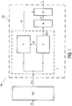
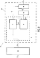
- An embodiment of the display device DD according to the invention as shown in Fig. 1 comprises an adjustable light source BL, a display panel DP with pixels for modulating light LB originating from the light source BL, and processing circuitry P.
- the processing circuitry P is coupled to the display panel DP and to the adjustable light source BL and has an input for receiving an input signal VI representing an image to be displayed on the display panel DP.
- the image may be represented by a matrix of rows and columns of pixels.
- the input signal represents a sequence of images.
- the input signal comprises sequences of parts of images, for example, even and odd fields of a video frame, then the image is to be interpreted also as such an even or odd field.
- the processing circuitry P comprises means for selecting a dimmed brightness level Lbdim of the light source BL in dependence on brightness levels, hereinafter also called gray levels, of pixels of the image to be displayed.
- the means for selecting may be hardware selection circuitry S as shown in Fig.1 or may be realized with software or a combination of both.
- the means for selecting processes the input signal VI and selects the dimmed brightness level Lbdim, thereby substantially minimizing an error function as will be explained later on.
- the selection circuitry S provides a light source drive signal BLD for adapting the brightness level LB of the light source BL to the dimmed brightness level Lbdim.
- the processing circuitry P further comprises means for adapting the input signal VI in dependence on the selected dimmed brightness level LBdim.
- the means for adapting may be hardware adaptation circuitry A as shown in Fig.1 or may be realized with software or a combination of both.
- the selection circuitry S provides an adaptation drive signal AD to the adaptation circuitry A in dependence on the selected dimmed brightness level Lbdim.
- the adaptation circuitry A adapts the input signal VI, thereby taking into account the adaptation drive signal AD and any other transformations required to adapt the input signal VI to an output signal V2, suitable for driving the display panel DP.
- transformations may include, amongst others, gamma correction, adaptation of the input signal VI to transmission characteristics of the display panel DP, and/ or adaptation of color components of the input signal VI to the primary colors of the display panel DP.
- the output signal V2 driving the display panel DP in combination with the brightness level of the light LB from the light source BL, determines the light output L of each of the pixels of the display panel.
- the input signal VI may be analog or digital; it may represent monochrome images or color images.
- the input signal may comprise a separate luminance signal in combination with color information or may comprise color components, for example in the form of an RGB signal with a red color component R, a green color component G and a blue color component B.
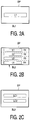
- the light source BL may be a single lamp backlight unit BL1 with one lamp L1 as shown in Fig. 2A for illuminating the whole display panel DP.
- it may be a multiple lamp backlight unit BL2 with a plurality of lamps L1, L2, L3, L4, each directed to illuminate a corresponding region R1, R2, R3, R4 of the display panel DP.
- Each of the lamps L1, L2, L3, L4 may be dimmed simultaneously with a substantially same amount or may be dimmed separately with a different amount and/ or at different moments in time.
- the effect of dimming one of the lamps L1, L2, L3, L4 for a particular one of the regions R1, R2, R3, R4 may result in a change of brightness levels in another region which overlaps with this particular region.
- the change of brightness levels may be corrected by adapting the output signal V2, such that this adaptation counteracts the changes. If one or more of the regions R1, R2, R3, R4 correspond, for example, to a horizontal (or vertical) black bar in an image to be displayed, the corresponding lamp L1; L2; L3; L4 may be turned off completely.
- a multicolor backlight unit BL3 with a plurality of color lamps LCI, LC2 of different color, the color lamps LC1, LC2 directed to illuminate a same region of the display panel DP.
- the light source may also be formed by alterations (for example of number, type or positions of lamps) and/ or combinations of above mentioned backlight units.
- the number of lamps may be equal to the number of pixels.
- a backlight unit having one or more lamps providing a substantially constant brightness, while dimming of the light is obtained by means of a light shutter, which controls the amount of light to be passed on from the lamps to the display panel DP.
- the light shutter may comprise parts which are controllable separately, so that the amount of light can be controlled per part of the area to be illuminated.
- the lamps may be any type of lamp, like fluorescent lamps, LEDs, or OLEDs.
- the display panel DP as shown in Fig. 1 may be a Liquid Crystal Display panel (LCD panel) or any other light-modulating panel, for example a panel with movable micro mirrors as used in a projector with Digital Mirror Devices.
- the LCD panel may be a transmissive LCD panel for modulating the light passing through the panel as shown in Fig. 1 or a reflective LCD that modulates the light reflected by the panel (not shown) or a transflective LCD which is capable of modulating both the transmitted and the reflected light.
- the display panel DP may be applied in a display product PR, for example, a television set, a monitor, a portable computer (laptop), a PDA or mobile phone equipped with a display.
- these products include signal processing circuitry SPC for processing signals received via an input terminal IN to convert them into the input signal V1 of the display module.
- the input terminal IN may be an antenna terminal or a connector via which a base band signal is received.
- the product PR may be a direct view display panel allowing a user to watch images on the display or a projection based system allowing the user to watch images projected from the display panel via an optical system on a screen.
- the projection system may be a rear or a front projection system.
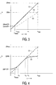
- Fig. 3 illustrating an embodiment with a digital monochrome input signal VI, representing gray levels x of the pixel of the image.
- the adaptation circuitry A may be designed to deliver an output signal V2, which results in a light output L of a display pixel as function of the gray level x of that corresponding pixel in the input signal according to the first curve C1.
- the light output L would be proportional to the gray level x from a zero gray level (black level) to a maximum available gray level x max (white level).
- the contrast ratio CR of a display panel such as an LCD panel, is limited to a value in the order of magnitude of 100 to 200.
- the lowest brightness that can be represented is Lbmax/ CR. This means that gray levels with a value below a threshold level x thres are not correctly displayed on the display panel DP: all dark gray values from 0 to x thres will have the light output Lbmax/ CR.
- a further improvement of the reproduction of dark gray levels is obtained up to a minimum gray level, being the dimmed threshold level x thresd which is smaller than x thres .
- This dimmed threshold level x thresd corresponds to the minimum brightness level Lbdim/ CR. This improvement is obtained at the expense of clipping of gray levels above a level x 1 corresponding to the dimmed brightness level Lbdim.
- the input signal V1 may include a gamma pre-correction function Gs(Ls) which is provided by a source from which the image is obtained.
- Ls represents the brightness of the image at the source.
- the display panel DP may have a gamma characteristic Gd that is different from the pre-correction function Gs.
- Ls Gdi Lbmax / Lbdim .
- Gsi x with Gdi and Gsi representing the inverse functions of Gd and Gs, respectively, a look-up table may be applied to determine the adapted gray level x' as function of the gray level x.
- the light BL may be dimmed. If the image contains many bright pixels with gray values close to x max and no values below x thres , then the light source BL may be driven to its maximum value Lbmax. When an image contains very few pixels with a gray level above x 1 and many pixels with a gray level below x thres , then the light source BL is preferably driven to the dimmed brightness level Lbdim.
- the dimmed brightness level Lbdim and the corresponding gray level x 1 may be determined dynamically for subsequent images (or per region of each of the subsequent images in case a multiple lamp backlight unit BL2 is applied).
- an image contains both pixels with gray levels above x 1 and below x thres , deterioration of the displayed image is inevitable and a compromise is necessary.
- an error function is applied which corresponds to the amount of deterioration of the displayed image. By selecting for each image a dimmed brightness level Lbdim which results in a minimum value of this error function, the deterioration is minimized.
- the error function includes a number of occurrences of gray levels x corresponding to a brightness level L above the dimmed brightness level Lbdim and/ or a number of occurrences of gray levels x corresponding to a brightness level L below a predetermined brightness level, which preferably corresponds to the minimum brightness level Lbdim/ CR.
- Dividing by the total number of pixels may be omitted, as this number is the same for all terms in the summation and results merely in the resulting error function to be scaled with the number of pixels.
- the weighting functions f(x), g(x) may be substantially equal to one, giving an equal weight to each of the gray levels above x 1 or below x thresd .
- the weighting functions may take into account information about pixels surrounding pixels with a same gray level x as explained in further detail below.
- Fig. 7 shows a part of an image comprising a matrix of rows i and columns j of pixels. Each pixel is identified by a combination of a row index i and a column index j.
- the indices i, j are determined for pixels having this gray level x.
- the weight factor f ij is determined for each of the pixels with the thus determined indices i, j. This weight factor f ij is determined taking into account the gray level of pixels surrounding the pixel with indices i, j.
- the row indices i of the surrounding pixels range SP from a lowest value of i minus an integer value i1 up to and including a highest value of i plus an integer value i2.
- the column indices j of the surrounding pixels range from a lowest value of j minus an integer value j1 up to and including a highest value of j plus an integer value j2.
- the pixel with indices i, j is of course to be excluded from the surrounding pixels SP.
- a suitable method to determine this weight factor f ij is to sum differences d(k1,k2) in gray levels between the surrounding pixels SP with indices k1, k2 and the pixel with indices i, j.
- the value f ij is calculated for each of the pixels having the gray value x.
- the final weight function f(x) associated with the gray level x may be the largest value f ij found for the pixels with this value of x.
- f(x) may be the sum of all weight factors f ij found for the pixels with this value of x.
- the term (x-x 1 ) represents the deviation of the displayed gray value from the gray value x of the input signal, hence is a measure for the amount of clipping.
- FIG. 4 Another embodiment with soft clipping is illustrated in Fig. 4 .
- the light output L as function of the gray level x is shown with x max being the maximum gray level.
- the first curve C1 shows again the curve for an ideal panel.
- a fourth curve C4 illustrates the soft clipping for a dimmed brightness level Lbdim. Between gray levels x 3 and x 2 the fourth curve C4 follows substantially the first curve C1, similar to the third curve C3 as shown in Fig. 3 . However the difference with the third curve C3 is that below the gray level x 3 the relation of the light output L versus the gray level x is gradually flattened. When the gray level x approaches zero, the light output approaches the minimum brightness level Lbdim/ CR.
- the third curve C3 shown in Fig. 3 all gray levels between zero and x thresd are rendered with the same minimum brightness level Lbdim/CR.
- the fourth curve C4 with soft clipping as shown in Fig. 4 the gray levels between zero and x thresd are rendered with a different brightness level. So, the gray levels below x thresd remain discernable, thereby improving the perceived image quality.
- the fourth curve C2 is flattened above x 2 in order to allow gray levels above x 1 to be discernable. This flattening may be non-linear as shown, but may also be linear from zero to x 3 and/ or from x 2 to x max to simplify the required processing.
- the embodiments illustrated in Figs. 3 and 4 may have look-up tables. These look-up tables comprise for each gray level of the input signal VI a corresponding value of the gray level of the output signal V2. When the display panel DP is driven with these corresponding gray values of the output signal V2, the light output L follows a curve as function of the gray level x as programmed in the look-up table.
- Whether soft clipping is applied or not may be made dependent on the amount of errors introduced in the light output L as function of the gray levels of the input signal V1. These errors result from clipping of the gray levels in the range from zero to x thresd and from x 1 to x max as, for example, is illustrated with the third curve C3 in Fig. 3 .
- the known method in the field of computer graphics of Bezier Curves may be applied as smoothing algorithm, in particular the quadratic form of the Bezier Curve.
- This quadratic form is simply a linear interpolation of the linear interpolation between three control points P 0 , P 1 , and P 2 as shown in Fig. 8 .
- the algorithm given below is iterated, indicated by the integers h and t, for a number of samples m on the smooth Bezier curve of the output signal V2 .
- the output gray levels y of the output signal V2 as function of the gray levels x of the input signal V1 are shown in Fig. 10 .
- the curve C4 corresponds to the curve C4 shown in Fig.
- the number of samples m may be selected to be equal to the number of gray levels between x max and x 2 .
- P 0 y thresd
- P 1 Y thresd
- P 2 y 3 .
- the value y 3 may be 2*y thresd , resulting in a number of samples m equal to x 3 .
- the processing circuitry P may be realized as shown in the block diagram of Fig. 5 .
- the selection circuitry S is adapted to select the dimmed brightness level Lbdim for which the sum of the error functions of each of the color component R1, G1, B1 is minimized.
- the gray levels of the color components R1, G1, B1 are to be interpreted as the amplitude levels of the color components R1, G1, B1.
- the sum may be determined based on a weighted addition of the error functions. The weighting may be based on the brightness contribution of each of the color components R1, G1, B1.
- the selection circuitry S provides the light source drive signal BLD, which adjusts the light source BL to the selected dimmed brightness level Lbdim.
- the selection circuitry also provides the adaptation drive signal AD.
- the adaptation circuitry A adapts the gray levels (amplitudes) of each of the color components in respective color component adjustment circuits AR, AG, AB. Due to the dimming the colors in dark gray areas of the image are reproduced more correctly as the amplitudes corresponding to these dark gray levels of each of the color components are discernable in the displayed image.
- further transformations may take place in the adaptation circuitry A. In case the display panel DP has primary colors differing from the primary colors of the input signal VI and/ or a different number of primary colors, then also the transformation from the primary colors of the input signal VI to the primary colors of the display panel DP may be included.
- the smoothing as described in the fifth step M5 may be set to respond faster to an increase of the dimmed brightness level Lbdim(n) during subsequent images. This may be achieved by selecting a different constant q during the increase.
- the advantage is, that clipping in white areas is reduced for images with white areas following a sequence of dark images.
- the relatively slow response during a decrease of the dimmed brightness level Lbdim(n) for subsequent images ensures that flickering of the displayed image is avoided.
- the smoothing may also take into account lamp parameters, for example at what rate a lamp is able to change its light output, or any limitations required to ensure an adequate lifetime of a lamp.
- the smoothing may also take into account actual operating conditions or historical operating conditions of a lamp.
- Fig. 9 shows a block diagram of an embodiment of the display device according to the invention, which uses feedback.
- the diagram is the same as the one shown in Fig. 1 , except that the input for the selection circuitry S is now the output signal V2.
- This means a feedback loop is present, wherein the selection circuitry S determines a dimmed brightness level Lbdim(n) for an n th image of a sequence of images and a corresponding adaptation drive signal AD on the basis of gray levels of the output signal V2 corresponding to the (n-1) th image.
- the display panel When dimming the light source BL and simultaneously compensating for the dimming by adapting the input signal VI, the display panel operates at a higher transmission (or reflection) rate. Especially for LCD panels, at this higher transmission rate the viewing angle increases. This means that dimming in combination with adapting the input signal VI as described hereinbefore has the additional advantage of improving the viewing angle for the dimmed images. Moreover a lamp of the light source requires less power when dimmed, so power is saved when dimming is applied. At the same time the lifetime of the lamp may be extended.
- a further advantage is, that when the amount of dimming takes into account the operating limits of the light source, it is possible to select firstly the amount of dimming which the light source is able to follow, and then to determine the corresponding adaptation of the input signal VI. So, any mismatch, caused by the fact that the light source is not able to follow the requested brightness changes of subsequent images, is avoided, thereby avoiding picture quality deterioration.
Description
- The invention relates to a display device comprising an adjustable light source, a display panel with display pixels for modulating light originating from the light source and processing circuitry coupled to the display panel and the adjustable light source.
-
EP 1,111,578 A1 discloses a display device with a passive light modulation part and a light source. A video signal is provided to the passive light modulation part for generating an image. The amplitude of the video signal is dynamically adjustable based on a detected minimum, maximum and average brightness value of the video signal. The brightness of the light source is adjustable in such a way that the image displayed on the passive light modulation part after the dynamic adjusting of the amplitude does not vary visually from an average brightness level for each frame of the video signal. It is a disadvantage of the known display device that this adjustment of the amplitude and the corresponding adjustment of the brightness of the light source do not provide for all images the best possible rendering of these images on the light modulation part. -
JP H11 65531 A -
US 2002/130830 A1 discloses a display device where the backlight brightness is adjusted in dependence on the comparison between the number of pixels having a gray level below a fixed lower threshold, and the number pixels having a gray level above a fixed upper threshold. - It is an object of the invention to provide a display device of the kind described in the opening paragraph, which has an alternative way of adjusting the amplitude of the video signal and the brightness of the light source.
- The object is realized in that the display device comprises an adjustable light source; a display panel with display pixels for modulating light originating from the light source; and processing circuitry coupled to the display panel and the adjustable light source, the processing circuitry having an input for receiving an input signal representing gray levels of pixels of an image to be displayed on the display panel and comprising:
- means for selecting a dimmed brightness level of the light source in dependence on the gray levels of the image pixels, and
- means for adapting the input signal in dependence on the dimmed brightness level.
- The invention is defined by the independent claims. The dependent claims define advantageous embodiments.
- Firstly the dimmed brightness level of the light source is determined. This enables the selection of a value that the light source is able to provide, thereby taking into account, for example, operating conditions or limitations of dynamic variations of the light source. As a next step, the processing circuitry adapts the input signal taking into account the selected brightness level. This sequence enables the selection of a matching combination for each image of a dimmed brightness level and an adapted input signal. The prior art disclosed in
EP 1,111,578 A1 firstly determines the adaptation of the amplitude of the input signal and thereafter determines the dimmed brightness level so as to match a brightness level of the input signal.US 5,717,422 discloses a display with a light source providing light to a light modulation part. A control is present for controlling the intensity of the light source as function of a brightness characteristic of an image to be displayed, while nothing is disclosed about adapting an input signal coupled to the modulation part in correspondence with the controlling of the intensity of the light source.US 6,631,995 discloses a device with a light source and a light control device. Via a video signal amplifier a light modulation panel is driven in such a way that the contrast of an image to be displayed by the device has a desired value. Via a light-control device, controlling the amount of light provided by the light source to the modulation panel, the image to be displayed is corrected such that the brightness of the displayed image corresponds with a desired value. So, this prior art, firstly determines the desired contrast, and then to what extent to control the amount of light provided by the light source. - In an embodiment the means for selecting is adapted to select the dimmed brightness level in dependence on a number of occurrences of a gray level corresponding to a brightness of display pixels above the dimmed brightness level and/ or a number of occurrences of a gray level corresponding to a brightness level of display pixels below a predetermined brightness level. Compared to the prior art disclosed in
EP 1,111,578 A1 , this invention provides generally a further dimming of the light source, resulting in an improved discernability of the dark gray levels corresponding to brightness levels near the minimum brightness level at the expense of some clipping of the gray levels corresponding to brightness levels near the dimmed brightness level. The predetermined level may be a fixed level, or, more preferably, an adjustable level, which is determined in dependence on the dimmed brightness level. - In an embodiment the predetermined brightness level is formed by the maximum contrast ratio of the display panel and the dimmed brightness level, preferably by dividing the dimmed brightness level by the contrast ratio. When selecting the dimmed brightness level it is important to take into account the resulting minimum brightness level that can be reproduced, as gray levels corresponding to a brightness level below this minimum obtainable brightness level are not correctly reproduced on the display device. When determining the predetermined brightness level, a suitable range of values is 50% to 150% of the ratio of the dimmed brightness level and contrast ratio, particularly a range of 80% to 100%.
- These and other aspects of the invention will be further elucidated and described with reference to the drawings, in which:
-
Fig. 1 shows a block diagram of an embodiment of the display device according to the invention; -
Figs. 2A to 2C show various backlight configurations which may be applied in the display device according to the invention; -
Fig. 3 shows a graph of the output luminance of the display panel versus the gray levels of the input signal of the display device illustrating the operation of an embodiment of the display device according to the invention; -
Fig. 4 shows another graph of the output luminance of the display panel versus the gray levels of the input signal of the display device illustrating the operation of another embodiment of the display device according to the invention; -
Fig. 5 shows a block diagram of an embodiment of processing circuitry applied in the display device according to the invention; -
Fig. 6 shows a flow diagram of an embodiment according to the invention; -
Fig. 7 shows a part of an image comprising a matrix of rows i and columns j of pixels; -
Fig. 8 shows an embodiment of an interpolation approach to obtain soft clipping according to the invention; -
Fig. 9 shows a block diagram of an embodiment of the display device according to the invention with feedback; and -
Fig. 10 shows a graph of the output gray levels of the output signal as function of the gray levels of the input signal. - The same references in different Figs. refer to the same signals or to elements performing the same function.
- An embodiment of the display device DD according to the invention as shown in
Fig. 1 comprises an adjustable light source BL, a display panel DP with pixels for modulating light LB originating from the light source BL, and processing circuitry P. The processing circuitry P is coupled to the display panel DP and to the adjustable light source BL and has an input for receiving an input signal VI representing an image to be displayed on the display panel DP. The image may be represented by a matrix of rows and columns of pixels. In case of a moving image (video), the input signal represents a sequence of images. In case the input signal comprises sequences of parts of images, for example, even and odd fields of a video frame, then the image is to be interpreted also as such an even or odd field. - The processing circuitry P comprises means for selecting a dimmed brightness level Lbdim of the light source BL in dependence on brightness levels, hereinafter also called gray levels, of pixels of the image to be displayed. The means for selecting may be hardware selection circuitry S as shown in
Fig.1 or may be realized with software or a combination of both. The means for selecting processes the input signal VI and selects the dimmed brightness level Lbdim, thereby substantially minimizing an error function as will be explained later on. The selection circuitry S provides a light source drive signal BLD for adapting the brightness level LB of the light source BL to the dimmed brightness level Lbdim. - The processing circuitry P further comprises means for adapting the input signal VI in dependence on the selected dimmed brightness level LBdim. The means for adapting may be hardware adaptation circuitry A as shown in
Fig.1 or may be realized with software or a combination of both. The selection circuitry S provides an adaptation drive signal AD to the adaptation circuitry A in dependence on the selected dimmed brightness level Lbdim. The adaptation circuitry A adapts the input signal VI, thereby taking into account the adaptation drive signal AD and any other transformations required to adapt the input signal VI to an output signal V2, suitable for driving the display panel DP. These other transformations may include, amongst others, gamma correction, adaptation of the input signal VI to transmission characteristics of the display panel DP, and/ or adaptation of color components of the input signal VI to the primary colors of the display panel DP. The output signal V2 driving the display panel DP, in combination with the brightness level of the light LB from the light source BL, determines the light output L of each of the pixels of the display panel. - The input signal VI may be analog or digital; it may represent monochrome images or color images. In case of color images, the input signal may comprise a separate luminance signal in combination with color information or may comprise color components, for example in the form of an RGB signal with a red color component R, a green color component G and a blue color component B. In case of color images, the term "gray level" is to be interpreted as an amplitude level of a color component. These gray levels or amplitude levels may be discrete levels in case of a digital input signal. For example, in case of an 8 bit digital signal 28 = 256 gray levels or amplitude levels are possible.
- The light source BL may be a single lamp backlight unit BL1 with one lamp L1 as shown in
Fig. 2A for illuminating the whole display panel DP. Alternatively, as shown inFig. 2B , it may be a multiple lamp backlight unit BL2 with a plurality of lamps L1, L2, L3, L4, each directed to illuminate a corresponding region R1, R2, R3, R4 of the display panel DP. Each of the lamps L1, L2, L3, L4 may be dimmed simultaneously with a substantially same amount or may be dimmed separately with a different amount and/ or at different moments in time. In case the regions R1, R2, R3, R4 partially overlap each other, the effect of dimming one of the lamps L1, L2, L3, L4 for a particular one of the regions R1, R2, R3, R4 may result in a change of brightness levels in another region which overlaps with this particular region. In such a case the change of brightness levels may be corrected by adapting the output signal V2, such that this adaptation counteracts the changes. If one or more of the regions R1, R2, R3, R4 correspond, for example, to a horizontal (or vertical) black bar in an image to be displayed, the corresponding lamp L1; L2; L3; L4 may be turned off completely. - Another alternative, as shown in
Fig. 2C , is a multicolor backlight unit BL3 with a plurality of color lamps LCI, LC2 of different color, the color lamps LC1, LC2 directed to illuminate a same region of the display panel DP. Of course, the light source may also be formed by alterations (for example of number, type or positions of lamps) and/ or combinations of above mentioned backlight units. The number of lamps may be equal to the number of pixels. - Yet another alternative (not shown) is a backlight unit, having one or more lamps providing a substantially constant brightness, while dimming of the light is obtained by means of a light shutter, which controls the amount of light to be passed on from the lamps to the display panel DP. The light shutter may comprise parts which are controllable separately, so that the amount of light can be controlled per part of the area to be illuminated.
- The lamps may be any type of lamp, like fluorescent lamps, LEDs, or OLEDs.
- The display panel DP as shown in
Fig. 1 may be a Liquid Crystal Display panel (LCD panel) or any other light-modulating panel, for example a panel with movable micro mirrors as used in a projector with Digital Mirror Devices. The LCD panel may be a transmissive LCD panel for modulating the light passing through the panel as shown inFig. 1 or a reflective LCD that modulates the light reflected by the panel (not shown) or a transflective LCD which is capable of modulating both the transmitted and the reflected light. - The display panel DP may be applied in a display product PR, for example, a television set, a monitor, a portable computer (laptop), a PDA or mobile phone equipped with a display. In general, these products include signal processing circuitry SPC for processing signals received via an input terminal IN to convert them into the input signal V1 of the display module. The input terminal IN may be an antenna terminal or a connector via which a base band signal is received. The product PR may be a direct view display panel allowing a user to watch images on the display or a projection based system allowing the user to watch images projected from the display panel via an optical system on a screen. The projection system may be a rear or a front projection system.
- For simplicity of the explanation, the principles of operation of the display device DD shown in
Fig. 1 , will be explained with reference toFig. 3 illustrating an embodiment with a digital monochrome input signal VI, representing gray levels x of the pixel of the image. - When setting the light source BL to a maximum brightness level LBmax , the adaptation circuitry A may be designed to deliver an output signal V2, which results in a light output L of a display pixel as function of the gray level x of that corresponding pixel in the input signal according to the first curve C1. In case of an ideal panel the light output L would be proportional to the gray level x from a zero gray level (black level) to a maximum available gray level xmax (white level). However, in practice the contrast ratio CR of a display panel, such as an LCD panel, is limited to a value in the order of magnitude of 100 to 200. As a result, the lowest brightness that can be represented is Lbmax/ CR. This means that gray levels with a value below a threshold level xthres are not correctly displayed on the display panel DP: all dark gray values from 0 to xthres will have the light output Lbmax/ CR.
- For some images it may be advantageous to dim the light of the light source BL to a dimmed brightness level Lbdim to improve the reproduction of these dark gray values. This is illustrated by the second curve C2. As a result of the dimming, the lowest possible brightness is now reduced to a minimum brightness level Lbdim/ CR as shown in
Fig. 3 . - By mapping the input signal V1 to the light output L according the third curve C3 a further improvement of the reproduction of dark gray levels is obtained up to a minimum gray level, being the dimmed threshold level xthresd which is smaller than xthres. This dimmed threshold level xthresd corresponds to the minimum brightness level Lbdim/ CR. This improvement is obtained at the expense of clipping of gray levels above a level x1 corresponding to the dimmed brightness level Lbdim.
- The input signal V1 may include a gamma pre-correction function Gs(Ls) which is provided by a source from which the image is obtained. The term Ls represents the brightness of the image at the source. The resulting gray level x of the input signal VI may be expressed as:

- The display panel DP may have a gamma characteristic Gd that is different from the pre-correction function Gs. When driven by an adapted gray level x' the display panel DP generates a light output L of:


- Depending on the content of an image, the light BL may be dimmed. If the image contains many bright pixels with gray values close to xmax and no values below xthres, then the light source BL may be driven to its maximum value Lbmax. When an image contains very few pixels with a gray level above x1 and many pixels with a gray level below xthres, then the light source BL is preferably driven to the dimmed brightness level Lbdim. The dimmed brightness level Lbdim and the corresponding gray level x1 may be determined dynamically for subsequent images (or per region of each of the subsequent images in case a multiple lamp backlight unit BL2 is applied). If an image contains both pixels with gray levels above x1 and below xthres, deterioration of the displayed image is inevitable and a compromise is necessary. In order to quantify the perceived deterioration of the displayed image, an error function is applied which corresponds to the amount of deterioration of the displayed image. By selecting for each image a dimmed brightness level Lbdim which results in a minimum value of this error function, the deterioration is minimized.
- The error function includes a number of occurrences of gray levels x corresponding to a brightness level L above the dimmed brightness level Lbdim and/ or a number of occurrences of gray levels x corresponding to a brightness level L below a predetermined brightness level, which preferably corresponds to the minimum brightness level Lbdim/ CR. An embodiment of the error function ETot(x1) is given by the formula:

- Dividing by the total number of pixels may be omitted, as this number is the same for all terms in the summation and results merely in the resulting error function to be scaled with the number of pixels.
- The weighting functions f(x), g(x) may be substantially equal to one, giving an equal weight to each of the gray levels above x1 or below xthresd.
- Alternatively, the weighting functions may take into account information about pixels surrounding pixels with a same gray level x as explained in further detail below.
-
Fig. 7 shows a part of an image comprising a matrix of rows i and columns j of pixels. Each pixel is identified by a combination of a row index i and a column index j. For a given gray level x above the gray level x1 (so, being a gray level which is clipped), the indices i, j are determined for pixels having this gray level x. Then for each of the pixels with the thus determined indices i, j, the weight factor fij is determined. This weight factor fij is determined taking into account the gray level of pixels surrounding the pixel with indices i, j. The row indices i of the surrounding pixels range SP from a lowest value of i minus an integer value i1 up to and including a highest value of i plus an integer value i2. The column indices j of the surrounding pixels range from a lowest value of j minus an integer value j1 up to and including a highest value of j plus an integer value j2. The pixel with indices i, j is of course to be excluded from the surrounding pixels SP. A suitable method to determine this weight factor fij is to sum differences d(k1,k2) in gray levels between the surrounding pixels SP with indices k1, k2 and the pixel with indices i, j. Only the surrounding pixels SP with a gray value larger than the gray level x of the pixel with indices i, j are taken into account, as this is an indication of the amount of clipping and of the amount of detail lost due to this clipping. So, the weight factor may be expressed as:
- The value fij is calculated for each of the pixels having the gray value x.
- The final weight function f(x) associated with the gray level x, may be the largest value fij found for the pixels with this value of x. Alternatively, f(x) may be the sum of all weight factors fij found for the pixels with this value of x.
- In another embodiment the weighting function f(x) is dependent on the amount of clipping as shown in below formula:

- Another embodiment with soft clipping is illustrated in
Fig. 4 . Like inFig. 3 , the light output L as function of the gray level x is shown with xmax being the maximum gray level. The first curve C1 shows again the curve for an ideal panel. A fourth curve C4 illustrates the soft clipping for a dimmed brightness level Lbdim. Between gray levels x3 and x2 the fourth curve C4 follows substantially the first curve C1, similar to the third curve C3 as shown inFig. 3 . However the difference with the third curve C3 is that below the gray level x3 the relation of the light output L versus the gray level x is gradually flattened. When the gray level x approaches zero, the light output approaches the minimum brightness level Lbdim/ CR. In the third curve C3 shown inFig. 3 , all gray levels between zero and xthresd are rendered with the same minimum brightness level Lbdim/CR. In the fourth curve C4 with soft clipping as shown inFig. 4 , the gray levels between zero and xthresd are rendered with a different brightness level. So, the gray levels below xthresd remain discernable, thereby improving the perceived image quality. Similarly, the fourth curve C2 is flattened above x2 in order to allow gray levels above x1 to be discernable. This flattening may be non-linear as shown, but may also be linear from zero to x3 and/ or from x2 to xmax to simplify the required processing. - The embodiments illustrated in
Figs. 3 and 4 may have look-up tables. These look-up tables comprise for each gray level of the input signal VI a corresponding value of the gray level of the output signal V2. When the display panel DP is driven with these corresponding gray values of the output signal V2, the light output L follows a curve as function of the gray level x as programmed in the look-up table. - Whether soft clipping is applied or not, may be made dependent on the amount of errors introduced in the light output L as function of the gray levels of the input signal V1. These errors result from clipping of the gray levels in the range from zero to xthresd and from x1 to xmax as, for example, is illustrated with the third curve C3 in
Fig. 3 . - The known method in the field of computer graphics of Bezier Curves may be applied as smoothing algorithm, in particular the quadratic form of the Bezier Curve. This quadratic form is simply a linear interpolation of the linear interpolation between three control points P 0, P 1, and P 2 as shown in
Fig. 8 . The algorithm given below is iterated, indicated by the integers h and t, for a number of samples m on the smooth Bezier curve of the output signal V2 . The output gray levels y of the output signal V2 as function of the gray levels x of the input signal V1 are shown inFig. 10 . Basically, the curve C4 corresponds to the curve C4 shown inFig. 4 , however now the relation with the output signal is shown instead of the relation with the light output L. The output gray levels y have been given the same indices as the corresponding gray levels x. The algorithm is:

- Soft clipping on the white levels is implemented using P 0 = y2 (chosen arbitrarily but must be smaller than ymax and greater than zero; see also
Fig. 10 ), P 1 = ymax and P 2 = ymax. The number of samples m may be selected to be equal to the number of gray levels between xmax and x2. - For soft clipping on the dark gray levels, P 0 = ythresd, P 1 = Ythresd and P 2 = y3. The value y3 may be 2*ythresd, resulting in a number of samples m equal to x3.
- If the input signal VI comprises color components, for example a red component R1, a green component G1 and a blue component B1, the processing circuitry P may be realized as shown in the block diagram of
Fig. 5 . The selection circuitry S is adapted to select the dimmed brightness level Lbdim for which the sum of the error functions of each of the color component R1, G1, B1 is minimized. The gray levels of the color components R1, G1, B1 are to be interpreted as the amplitude levels of the color components R1, G1, B1. The sum may be determined based on a weighted addition of the error functions. The weighting may be based on the brightness contribution of each of the color components R1, G1, B1. - The selection circuitry S provides the light source drive signal BLD, which adjusts the light source BL to the selected dimmed brightness level Lbdim. The selection circuitry also provides the adaptation drive signal AD. Based on this adaptation drive signal AD the adaptation circuitry A adapts the gray levels (amplitudes) of each of the color components in respective color component adjustment circuits AR, AG, AB. Due to the dimming the colors in dark gray areas of the image are reproduced more correctly as the amplitudes corresponding to these dark gray levels of each of the color components are discernable in the displayed image. As mentioned before, further transformations may take place in the adaptation circuitry A. In case the display panel DP has primary colors differing from the primary colors of the input signal VI and/ or a different number of primary colors, then also the transformation from the primary colors of the input signal VI to the primary colors of the display panel DP may be included.
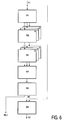
- A further embodiment is illustrated with the flow diagram shown in
Fig. 6 : - In a first step M1 the input signal VI, representing an image to be displayed, is analyzed to detect regions of the image which should be excluded from further analysis. In case of a sequence of images, for example representing video images, the flow chart is repeated for each subsequent image of the sequence of images. Regions to be excluded may be black bars appearing at the top and bottom of the screen, black bars at the left and right side, subtitling, on-screen displays and/or any other information inserted in a video image. Detection of, for example, black bars is well known and is not elaborated further.
- In a second step M2 a histogram is determined for each of the color components R1, G1, B1 of the input signal V1. Each histogram provides the number of occurrences of the gray levels (amplitudes) of the corresponding color component R1, G1, B1. The histograms may comprise data for all the regions or only for the regions which are not excluded in the first step M1.
- In a third step M3 the error function is determined for each of the color components R1, G1, B1 for a given dimmed brightness level Lbdim.
- In a fourth step M4 the error functions of the color components R1, G1, B1 are added. If the value of the error function is not the minimum value, the third step M3 and the fourth step M4 may be repeated for different values of the dimmed brightness level Lbdim until the value of the dimmed brightness level Lbdim has been found which corresponds to the minimum value of the error function for that image. Optionally, in order to save power, for example when a power save mode is selected by a user of the display module, dimming may also be applied to images which would not be dimmed according to the above-described flow diagram. In this case, the amount of dimming may be made dependent on the value of the resulting error function.
- In a fifth optional step M5 smoothing is applied to avoid flickering of the displayed image by abrupt changes of the dimmed brightness level Lbdim for subsequent images. The smoothing may be obtained by making the value of the dimmed brightness level Lbdim dependent on a smoothed dimmed brightness level Lbdim applied to a previous image. For example, the smoothed dimmed brightness level LbdimS(n) for an n-th image in a sequence of images is given by:

- Finally in a sixth step M6 the gray level x1 corresponding to the selected smoothed dimmed brightness level Lbdim is used to determine according to which curve the gray levels of the input signal VI should be adapted, for example according to the third curve C3 as shown in
Fig. 3 . Optionally soft clipping may be applied by as explained hereinbefore by applying the fourth curve C4 as shown inFig. 4 . - The smoothing as described in the fifth step M5 may be set to respond faster to an increase of the dimmed brightness level Lbdim(n) during subsequent images. This may be achieved by selecting a different constant q during the increase. The advantage is, that clipping in white areas is reduced for images with white areas following a sequence of dark images. At the same time the relatively slow response during a decrease of the dimmed brightness level Lbdim(n) for subsequent images, ensures that flickering of the displayed image is avoided. A suitable value for the constant q is 0.95 during a sequence of increasing dimmed brightness levels Lbdim(n) and q=0.05 during other sequences.
- The smoothing may also take into account lamp parameters, for example at what rate a lamp is able to change its light output, or any limitations required to ensure an adequate lifetime of a lamp. The smoothing may also take into account actual operating conditions or historical operating conditions of a lamp.
-
Fig. 9 shows a block diagram of an embodiment of the display device according to the invention, which uses feedback. The diagram is the same as the one shown inFig. 1 , except that the input for the selection circuitry S is now the output signal V2. This means a feedback loop is present, wherein the selection circuitry S determines a dimmed brightness level Lbdim(n) for an nth image of a sequence of images and a corresponding adaptation drive signal AD on the basis of gray levels of the output signal V2 corresponding to the (n-1)th image. - When dimming the light source BL and simultaneously compensating for the dimming by adapting the input signal VI, the display panel operates at a higher transmission (or reflection) rate. Especially for LCD panels, at this higher transmission rate the viewing angle increases. This means that dimming in combination with adapting the input signal VI as described hereinbefore has the additional advantage of improving the viewing angle for the dimmed images. Moreover a lamp of the light source requires less power when dimmed, so power is saved when dimming is applied. At the same time the lifetime of the lamp may be extended.
- A further advantage is, that when the amount of dimming takes into account the operating limits of the light source, it is possible to select firstly the amount of dimming which the light source is able to follow, and then to determine the corresponding adaptation of the input signal VI. So, any mismatch, caused by the fact that the light source is not able to follow the requested brightness changes of subsequent images, is avoided, thereby avoiding picture quality deterioration.
- It should be noted that the above-mentioned embodiments illustrate rather than limit the invention, and that those skilled in the art will be able to design many alternative embodiments without departing from the scope of the appended claims. For example, the allocation of the features in the various blocks of software or hardware may be changed without departing from the scope of the appended claims.
Claims (17)
- Processing circuitry (P) having:- an input for receiving an input signal (V1) representing gray levels of pixels of an image to be displayed on a display panel (DP) of a display device (DD), the display device (DD) comprising an adjustable light source (BL), the display panel (DP) having display pixels for modulating light originating from the light source (BL);- outputs for coupling to the display panel (DP) and the light source (BL);- means for selecting (S) a dimmed brightness level of the light source (BL) in dependence on the gray levels of the image pixels; and- means for adapting (A) the input signal (V1) in dependence on the dimmed brightness level, characterized in that
the means for selecting (S) are adapted to select the dimmed brightness level in dependence on: (i) a number of occurrences of a gray level corresponding to a brightness level of display pixels above the dimmed brightness level, and (ii) a number of occurrences of a gray level corresponding to a brightness level of display pixels below a predetermined brightness level being a fixed or adjustable level determined in dependence on the dimmed brightness level, wherein the predetermined brightness level is lower than the dimmed brightness level. - A display device (DD) comprising the adjustable light source (BL); the display panel (DP) having display pixels for modulating light originating from the light source (BL); and the processing circuitry (P) as claimed in claim 1.
- A display device (DD) as claimed in claim 2, wherein the means for selecting (S) being adapted to select the dimmed brightness level in dependence on the number of occurrences of the gray level corresponding to the brightness level of display pixels above the dimmed brightness level and the number of occurrences of the gray level corresponding to the brightness level of display pixels below the predetermined brightness level being the fixed or adjustable level determined in dependence on the dimmed brightness level.
- A display device (DD) as claimed in claim 2 or 3, the means for selecting (S) being adapted to substantially minimize an error function including one or more weighted numbers of occurrences formed by multiplying each of the one or more numbers of occurrences by a weighting factor.
- A display device (DD) as claimed in claim 4, the error function being formed by an addition of the one or more weighted numbers of occurrences.
- A display device (DD) as claimed in claim 5, the error function being substantially:

- A display device (DD) as claimed in claim 6, the weighting functions (f(x), g(x)) being substantially equal to one.
- A display device (DD) as claimed in claim 6, at least one of the weighting functions (f(x), g(x)) being formed by a sum (fij) of deviations (d(k1,k2)) of gray levels between a pixel and its neighboring pixels, with k1, k2 being indices identifying the neighboring pixels.
- A display device (DD) as claimed in claim 8, the pixel being the pixel having the highest sum (fij) of all pixels with this gray level in an image.
- A display device (DD) as claimed in claim 6, at least one of the weighting functions (f(x), g(x)) being formed by a deviation of the gray level from a gray level corresponding to the dimmed brightness level or by a deviation from a gray level corresponding to the predetermined brightness level.
- A display device (DD) as claimed in claim 3, the predetermined brightness level being formed by the maximum contrast ratio of the display panel (DP) and the dimmed brightness level.
- A display device (DD) as claimed in claim 4, the input signal (V1) comprising color components (R1, G1, B1) of the image, a component error function being determined for each of the color components (R1, G1, B1), the error function being formed by adding the component error functions.
- A display device (DD) as claimed in claim 2, the processing circuitry (P) further comprising means for determining a smoothed dimmed brightness level (Lbdim S(n)) for an image in dependence on the dimmed brightness level (Lbdim (n)) of the image and a previous smoothed dimmed brightness level (LbdimS(n-1)) of a previous image, wherein n is a sequence number of successive images.
- A display device (DD) as claimed in claim 13, the smoothing having a faster response time to an increasing dimmed brightness level of subsequent images than to a decreasing dimmed brightness level of subsequent images.
- A display device (DD) as claimed in claim 2, wherein the means for selecting (S) a dimmed brightness level are further adapted to select the dimmed brightness level in dependence on a content of a part of the image.
- A method of adjusting a light source (BL) of a display device (DD), the display device (DD) comprising a display panel (DP) having display pixels for modulating light originating from the light source (BL); and processing circuitry (P) coupled to the display panel (DP) and the light source (BL), the processing circuitry (P) having an input for receiving an input signal (V1) representing gray levels of pixels of an image to be displayed on the display panel (DP), the method comprising:- selecting (S) a dimmed brightness level of the light source (BL) in dependence on the gray levels of the image pixels, and- adapting (A) the input signal (V1) in dependence on the dimmed brightness level, characterized in that
the selecting (S) selects the dimmed brightness level in dependence on: (i) a number of occurrences of a gray level corresponding to a brightness level of display pixels above the dimmed brightness level, and (ii) a number of occurrences of a gray level corresponding to a brightness level of display pixels below a predetermined brightness level being a fixed or adjustable level determined in dependence on the dimmed brightness level, wherein the predetermined brightness level is lower than the dimmed brightness level. - A product (PR) comprising the display device (DD) as claimed in claim 2, and signal processing circuitry (SPC) for providing the input signal (V1).
Priority Applications (2)
| Application Number | Priority Date | Filing Date | Title |
|---|---|---|---|
| EP05709008.6A EP1733372B1 (en) | 2004-03-26 | 2005-03-15 | Display device comprising an adjustable light source |
| PL05709008T PL1733372T3 (en) | 2004-03-26 | 2005-03-15 | Display device comprising an adjustable light source |
Applications Claiming Priority (3)
| Application Number | Priority Date | Filing Date | Title |
|---|---|---|---|
| EP04101258 | 2004-03-26 | ||
| PCT/IB2005/050901 WO2005093703A1 (en) | 2004-03-26 | 2005-03-15 | Display device comprising an adjustable light source |
| EP05709008.6A EP1733372B1 (en) | 2004-03-26 | 2005-03-15 | Display device comprising an adjustable light source |
Publications (2)
| Publication Number | Publication Date |
|---|---|
| EP1733372A1 EP1733372A1 (en) | 2006-12-20 |
| EP1733372B1 true EP1733372B1 (en) | 2019-05-15 |
Family
ID=34961264
Family Applications (1)
| Application Number | Title | Priority Date | Filing Date |
|---|---|---|---|
| EP05709008.6A Active EP1733372B1 (en) | 2004-03-26 | 2005-03-15 | Display device comprising an adjustable light source |
Country Status (9)
| Country | Link |
|---|---|
| US (2) | USRE45209E1 (en) |
| EP (1) | EP1733372B1 (en) |
| JP (1) | JP4937108B2 (en) |
| KR (1) | KR20070005637A (en) |
| CN (1) | CN100555387C (en) |
| ES (1) | ES2738001T3 (en) |
| PL (1) | PL1733372T3 (en) |
| TR (1) | TR201910283T4 (en) |
| WO (1) | WO2005093703A1 (en) |
Families Citing this family (61)
| Publication number | Priority date | Publication date | Assignee | Title |
|---|---|---|---|---|
| US9083969B2 (en) | 2005-08-12 | 2015-07-14 | Sharp Laboratories Of America, Inc. | Methods and systems for independent view adjustment in multiple-view displays |
| US7982707B2 (en) | 2004-12-02 | 2011-07-19 | Sharp Laboratories Of America, Inc. | Methods and systems for generating and applying image tone scale adjustments |
| US8111265B2 (en) | 2004-12-02 | 2012-02-07 | Sharp Laboratories Of America, Inc. | Systems and methods for brightness preservation using a smoothed gain image |
| US7961199B2 (en) | 2004-12-02 | 2011-06-14 | Sharp Laboratories Of America, Inc. | Methods and systems for image-specific tone scale adjustment and light-source control |
| US8913089B2 (en) | 2005-06-15 | 2014-12-16 | Sharp Laboratories Of America, Inc. | Methods and systems for enhancing display characteristics with frequency-specific gain |
| US8922594B2 (en) | 2005-06-15 | 2014-12-30 | Sharp Laboratories Of America, Inc. | Methods and systems for enhancing display characteristics with high frequency contrast enhancement |
| US7924261B2 (en) | 2004-12-02 | 2011-04-12 | Sharp Laboratories Of America, Inc. | Methods and systems for determining a display light source adjustment |
| US8120570B2 (en) * | 2004-12-02 | 2012-02-21 | Sharp Laboratories Of America, Inc. | Systems and methods for tone curve generation, selection and application |
| US8004511B2 (en) | 2004-12-02 | 2011-08-23 | Sharp Laboratories Of America, Inc. | Systems and methods for distortion-related source light management |
| US8947465B2 (en) | 2004-12-02 | 2015-02-03 | Sharp Laboratories Of America, Inc. | Methods and systems for display-mode-dependent brightness preservation |
| JP4059910B2 (en) * | 2005-11-11 | 2008-03-12 | シャープ株式会社 | Liquid crystal display |
| US7733357B2 (en) | 2006-01-13 | 2010-06-08 | Hewlett-Packard Development Company, L.P. | Display system |
| KR101469537B1 (en) * | 2006-05-15 | 2014-12-05 | 티피 비전 홀딩 비.브이. | Method and device for driving an image display apparatus |
| JP4203081B2 (en) * | 2006-05-19 | 2008-12-24 | 株式会社東芝 | Image display device and image display method |
| PL2082391T3 (en) * | 2006-11-09 | 2015-06-30 | Koninklijke Philips Nv | Liquid crystal display system and method |
| WO2008088892A2 (en) * | 2007-01-19 | 2008-07-24 | Pixtronix, Inc. | Sensor-based feedback for display apparatus |
| JP5117762B2 (en) * | 2007-05-18 | 2013-01-16 | 株式会社半導体エネルギー研究所 | Liquid crystal display |
| TWI479891B (en) | 2007-06-26 | 2015-04-01 | Apple Inc | Dynamic backlight adaptation |
| TWI466093B (en) * | 2007-06-26 | 2014-12-21 | Apple Inc | Management techniques for video playback |
| JP5127321B2 (en) * | 2007-06-28 | 2013-01-23 | 株式会社東芝 | Image display device, image display method, and image display program |
| JP2009085990A (en) * | 2007-09-27 | 2009-04-23 | Sanyo Electric Co Ltd | Image display apparatus and controller |
| US8155434B2 (en) | 2007-10-30 | 2012-04-10 | Sharp Laboratories Of America, Inc. | Methods and systems for image enhancement |
| US8345038B2 (en) | 2007-10-30 | 2013-01-01 | Sharp Laboratories Of America, Inc. | Methods and systems for backlight modulation and brightness preservation |
| JP4655079B2 (en) * | 2007-11-06 | 2011-03-23 | ソニー株式会社 | Liquid crystal display device, liquid crystal display module, and liquid crystal display device driving method |
| US9177509B2 (en) | 2007-11-30 | 2015-11-03 | Sharp Laboratories Of America, Inc. | Methods and systems for backlight modulation with scene-cut detection |
| US8378956B2 (en) | 2007-11-30 | 2013-02-19 | Sharp Laboratories Of America, Inc. | Methods and systems for weighted-error-vector-based source light selection |
| EP2221801A4 (en) * | 2007-12-20 | 2011-02-23 | Sharp Kk | Display device |
| US8766902B2 (en) | 2007-12-21 | 2014-07-01 | Apple Inc. | Management techniques for video playback |
| US8179363B2 (en) * | 2007-12-26 | 2012-05-15 | Sharp Laboratories Of America, Inc. | Methods and systems for display source light management with histogram manipulation |
| US8169431B2 (en) * | 2007-12-26 | 2012-05-01 | Sharp Laboratories Of America, Inc. | Methods and systems for image tonescale design |
| US8203579B2 (en) * | 2007-12-26 | 2012-06-19 | Sharp Laboratories Of America, Inc. | Methods and systems for backlight modulation with image characteristic mapping |
| US8223113B2 (en) | 2007-12-26 | 2012-07-17 | Sharp Laboratories Of America, Inc. | Methods and systems for display source light management with variable delay |
| US8207932B2 (en) * | 2007-12-26 | 2012-06-26 | Sharp Laboratories Of America, Inc. | Methods and systems for display source light illumination level selection |
| US8493313B2 (en) | 2008-02-13 | 2013-07-23 | Dolby Laboratories Licensing Corporation | Temporal filtering of video signals |
| US9083519B2 (en) | 2008-02-29 | 2015-07-14 | Sharp Laboratories Of America, Inc. | Systems and methods for adaptively selecting a decoding scheme to decode embedded information |
| US9443489B2 (en) * | 2008-04-28 | 2016-09-13 | Au Optronics Corp. | Gamma curve compensating method, gamma curve compensating circuit and display system using the same |
| US8531379B2 (en) | 2008-04-28 | 2013-09-10 | Sharp Laboratories Of America, Inc. | Methods and systems for image compensation for ambient conditions |
| US8416179B2 (en) | 2008-07-10 | 2013-04-09 | Sharp Laboratories Of America, Inc. | Methods and systems for color preservation with a color-modulated backlight |
| US9330630B2 (en) | 2008-08-30 | 2016-05-03 | Sharp Laboratories Of America, Inc. | Methods and systems for display source light management with rate change control |
| JP2010066714A (en) * | 2008-09-12 | 2010-03-25 | Sharp Corp | Liquid crystal display and led backlight control method for the liquid crystal display |
| KR101348700B1 (en) * | 2008-12-01 | 2014-01-22 | 엘지디스플레이 주식회사 | Liquid crystal display device and method of driving the same |
| KR101589138B1 (en) * | 2008-12-09 | 2016-01-28 | 삼성디스플레이 주식회사 | Method for driving a light source light source apparatus for performing the method and display apparatus having the light source apparatus |
| JP2012529081A (en) * | 2009-06-03 | 2012-11-15 | マニュファクチャリング・リソーシズ・インターナショナル・インコーポレーテッド | LED backlight dynamic dimming |
| US8902149B2 (en) * | 2009-06-17 | 2014-12-02 | Sharp Laboratories Of America, Inc. | Methods and systems for power control event responsive display devices |
| US8165724B2 (en) | 2009-06-17 | 2012-04-24 | Sharp Laboratories Of America, Inc. | Methods and systems for power-controlling display devices |
| JP2012002936A (en) * | 2010-06-15 | 2012-01-05 | Fujitsu Ten Ltd | Display control device, display apparatus, and display control method |
| US8717278B2 (en) | 2010-08-31 | 2014-05-06 | Dolby Laboratories Licensing Corporation | Method and apparatus for adjusting drive values for dual modulation displays |
| CN102542995A (en) * | 2010-12-22 | 2012-07-04 | 深圳富泰宏精密工业有限公司 | Backlight regulating circuit |
| US9370064B2 (en) | 2011-10-06 | 2016-06-14 | National Semiconductor Corporation | LED driver having non-linear compensation |
| US8749538B2 (en) | 2011-10-21 | 2014-06-10 | Qualcomm Mems Technologies, Inc. | Device and method of controlling brightness of a display based on ambient lighting conditions |
| US9183812B2 (en) | 2013-01-29 | 2015-11-10 | Pixtronix, Inc. | Ambient light aware display apparatus |
| US9348174B2 (en) | 2013-03-14 | 2016-05-24 | Manufacturing Resources International, Inc. | Rigid LCD assembly |
| US10191212B2 (en) | 2013-12-02 | 2019-01-29 | Manufacturing Resources International, Inc. | Expandable light guide for backlight |
| CN103714775B (en) * | 2013-12-30 | 2016-06-01 | 北京京东方光电科技有限公司 | Pel array and driving method, display panel and display unit |
| US10649273B2 (en) | 2014-10-08 | 2020-05-12 | Manufacturing Resources International, Inc. | LED assembly for transparent liquid crystal display and static graphic |
| US10261362B2 (en) | 2015-09-01 | 2019-04-16 | Manufacturing Resources International, Inc. | Optical sheet tensioner |
| JP6971031B2 (en) * | 2017-01-13 | 2021-11-24 | シナプティクス・ジャパン合同会社 | Display driver, display device and drive method |
| WO2019099674A1 (en) * | 2017-11-16 | 2019-05-23 | Synaptics Incorporated | Plural gammas control technology for display panel |
| TWI678109B (en) * | 2018-05-02 | 2019-11-21 | 奇景光電股份有限公司 | Image processing method and display device for local dimming |
| CN110534067B (en) * | 2018-05-24 | 2021-06-22 | 奇景光电股份有限公司 | Image processing method and display device for regional dimming |
| TWI746201B (en) * | 2020-10-06 | 2021-11-11 | 瑞軒科技股份有限公司 | Display device and image correction method |
Citations (3)
| Publication number | Priority date | Publication date | Assignee | Title |
|---|---|---|---|---|
| EP0513551A2 (en) * | 1991-04-17 | 1992-11-19 | Casio Computer Company Limited | Image display apparatus |
| JPH1165531A (en) * | 1997-08-20 | 1999-03-09 | Fujitsu Ltd | Image display device and lsi for image display |
| US20020130830A1 (en) * | 2001-03-15 | 2002-09-19 | Park Cheol-Woo | LCD with adaptive luminance intensifying function and driving method thereof |
Family Cites Families (11)
| Publication number | Priority date | Publication date | Assignee | Title |
|---|---|---|---|---|
| US5717422A (en) * | 1994-01-25 | 1998-02-10 | Fergason; James L. | Variable intensity high contrast passive display |
| JPH11175027A (en) * | 1997-12-08 | 1999-07-02 | Hitachi Ltd | Liquid crystal driving circuit and liquid crystal display device |
| TWI249630B (en) | 1999-05-10 | 2006-02-21 | Matsushita Electric Ind Co Ltd | Image display device and method for displaying image |
| US6631995B2 (en) | 1999-09-02 | 2003-10-14 | Koninklijke Philips Electronics N.V. | Method of and device for generating an image having a desired brightness |
| JP4574057B2 (en) * | 2000-05-08 | 2010-11-04 | キヤノン株式会社 | Display device |
| JP2002202767A (en) * | 2000-10-25 | 2002-07-19 | Samsung Electronics Co Ltd | Liquid crystal display device, its drive unit and its method |
| US6636005B2 (en) | 2001-11-14 | 2003-10-21 | Koninklijke Philips Eletronics N.V. | Architecture of ballast with integrated RF interface |
| JP3652352B2 (en) * | 2001-12-27 | 2005-05-25 | エルジー電子株式会社 | Method and apparatus for driving flat panel display device |
| EP1367558A3 (en) | 2002-05-29 | 2008-08-27 | Matsushita Electric Industrial Co., Ltd. | Image display method and apparatus comprising luminance adjustment of a light source |
| EP1573708A1 (en) * | 2002-11-27 | 2005-09-14 | Koninklijke Philips Electronics N.V. | Method of improving the perceptual contrast of displayed images |
| JP3661692B2 (en) * | 2003-05-30 | 2005-06-15 | セイコーエプソン株式会社 | Illumination device, projection display device, and driving method thereof |
-
2005
- 2005-03-15 JP JP2007504529A patent/JP4937108B2/en active Active
- 2005-03-15 PL PL05709008T patent/PL1733372T3/en unknown
- 2005-03-15 EP EP05709008.6A patent/EP1733372B1/en active Active
- 2005-03-15 WO PCT/IB2005/050901 patent/WO2005093703A1/en active Application Filing
- 2005-03-15 US US14/080,212 patent/USRE45209E1/en active Active
- 2005-03-15 CN CNB2005800095833A patent/CN100555387C/en active Active
- 2005-03-15 KR KR1020067019470A patent/KR20070005637A/en not_active Application Discontinuation
- 2005-03-15 TR TR2019/10283T patent/TR201910283T4/en unknown
- 2005-03-15 ES ES05709008T patent/ES2738001T3/en active Active
- 2005-03-15 US US10/599,263 patent/US8059082B2/en not_active Ceased
Patent Citations (3)
| Publication number | Priority date | Publication date | Assignee | Title |
|---|---|---|---|---|
| EP0513551A2 (en) * | 1991-04-17 | 1992-11-19 | Casio Computer Company Limited | Image display apparatus |
| JPH1165531A (en) * | 1997-08-20 | 1999-03-09 | Fujitsu Ltd | Image display device and lsi for image display |
| US20020130830A1 (en) * | 2001-03-15 | 2002-09-19 | Park Cheol-Woo | LCD with adaptive luminance intensifying function and driving method thereof |
Also Published As
| Publication number | Publication date |
|---|---|
| CN100555387C (en) | 2009-10-28 |
| US8059082B2 (en) | 2011-11-15 |
| CN1934614A (en) | 2007-03-21 |
| TR201910283T4 (en) | 2019-08-21 |
| KR20070005637A (en) | 2007-01-10 |
| JP4937108B2 (en) | 2012-05-23 |
| ES2738001T3 (en) | 2020-01-17 |
| USRE45209E1 (en) | 2014-10-28 |
| WO2005093703A1 (en) | 2005-10-06 |
| PL1733372T3 (en) | 2019-11-29 |
| EP1733372A1 (en) | 2006-12-20 |
| JP2007530998A (en) | 2007-11-01 |
| US20080238840A1 (en) | 2008-10-02 |
Similar Documents
| Publication | Publication Date | Title |
|---|---|---|
| EP1733372B1 (en) | Display device comprising an adjustable light source | |
| EP2513892B1 (en) | Method and system for backlight control using statistical attributes of image data blocks | |
| US8619102B2 (en) | Display apparatus and method for adjusting brightness thereof | |
| US8610654B2 (en) | Correction of visible mura distortions in displays using filtered mura reduction and backlight control | |
| US20150262534A1 (en) | Display apparatus and brightness adjusting method thereof | |
| US8314767B2 (en) | Methods and systems for reducing view-angle-induced color shift | |
| US7859499B2 (en) | Display apparatus | |
| US8358293B2 (en) | Method for driving light source blocks, driving unit for performing the method and display apparatus having the driving unit | |
| US8593391B2 (en) | Liquid crystal display device control circuit and liquid crystal display system, which adjust brightness of display image by using height distribution of gradations of input image | |
| US20060071936A1 (en) | Method of improving the perceptual contrast of displayed images | |
| US8155435B2 (en) | Display apparatus and its control method | |
| US8259127B2 (en) | Systems and methods for reducing desaturation of images rendered on high brightness displays | |
| KR101073006B1 (en) | Display device and method for controling brightness of images in display device | |
| KR101389359B1 (en) | Display apparatus and method of adjusting brightness for the same | |
| US7312781B2 (en) | Method for dynamically modulating driving current of backlight module | |
| EP1982321B1 (en) | Histogram detector for contrast ratio enhancement system | |
| CN101568955B (en) | Method of determining luminance values for a backlight of an LCD panel displaying an image |
Legal Events
| Date | Code | Title | Description |
|---|---|---|---|
| PUAI | Public reference made under article 153(3) epc to a published international application that has entered the european phase |
Free format text: ORIGINAL CODE: 0009012 |
|
| 17P | Request for examination filed |
Effective date: 20061026 |
|
| AK | Designated contracting states |
Kind code of ref document: A1 Designated state(s): AT BE BG CH CY CZ DE DK EE ES FI FR GB GR HU IE IS IT LI LT LU MC NL PL PT RO SE SI SK TR |
|
| DAX | Request for extension of the european patent (deleted) | ||
| 17Q | First examination report despatched |
Effective date: 20080721 |
|
| RAP1 | Party data changed (applicant data changed or rights of an application transferred) |
Owner name: KONINKLIJKE PHILIPS N.V. |
|
| STAA | Information on the status of an ep patent application or granted ep patent |
Free format text: STATUS: EXAMINATION IS IN PROGRESS |
|
| GRAP | Despatch of communication of intention to grant a patent |
Free format text: ORIGINAL CODE: EPIDOSNIGR1 |
|
| STAA | Information on the status of an ep patent application or granted ep patent |
Free format text: STATUS: GRANT OF PATENT IS INTENDED |
|
| INTG | Intention to grant announced |
Effective date: 20181025 |
|
| GRAS | Grant fee paid |
Free format text: ORIGINAL CODE: EPIDOSNIGR3 |
|
| GRAA | (expected) grant |
Free format text: ORIGINAL CODE: 0009210 |
|
| STAA | Information on the status of an ep patent application or granted ep patent |
Free format text: STATUS: THE PATENT HAS BEEN GRANTED |
|
| AK | Designated contracting states |
Kind code of ref document: B1 Designated state(s): AT BE BG CH CY CZ DE DK EE ES FI FR GB GR HU IE IS IT LI LT LU MC NL PL PT RO SE SI SK TR |
|
| REG | Reference to a national code |
Ref country code: CH Ref legal event code: EP Ref country code: GB Ref legal event code: FG4D |
|
| REG | Reference to a national code |
Ref country code: DE Ref legal event code: R096 Ref document number: 602005055782 Country of ref document: DE |
|
| REG | Reference to a national code |
Ref country code: IE Ref legal event code: FG4D |
|
| REG | Reference to a national code |
Ref country code: NL Ref legal event code: MP Effective date: 20190515 |
|
| REG | Reference to a national code |
Ref country code: LT Ref legal event code: MG4D |
|
| PG25 | Lapsed in a contracting state [announced via postgrant information from national office to epo] |
Ref country code: PT Free format text: LAPSE BECAUSE OF FAILURE TO SUBMIT A TRANSLATION OF THE DESCRIPTION OR TO PAY THE FEE WITHIN THE PRESCRIBED TIME-LIMIT Effective date: 20190915 Ref country code: SE Free format text: LAPSE BECAUSE OF FAILURE TO SUBMIT A TRANSLATION OF THE DESCRIPTION OR TO PAY THE FEE WITHIN THE PRESCRIBED TIME-LIMIT Effective date: 20190515 Ref country code: NL Free format text: LAPSE BECAUSE OF FAILURE TO SUBMIT A TRANSLATION OF THE DESCRIPTION OR TO PAY THE FEE WITHIN THE PRESCRIBED TIME-LIMIT Effective date: 20190515 Ref country code: LT Free format text: LAPSE BECAUSE OF FAILURE TO SUBMIT A TRANSLATION OF THE DESCRIPTION OR TO PAY THE FEE WITHIN THE PRESCRIBED TIME-LIMIT Effective date: 20190515 Ref country code: FI Free format text: LAPSE BECAUSE OF FAILURE TO SUBMIT A TRANSLATION OF THE DESCRIPTION OR TO PAY THE FEE WITHIN THE PRESCRIBED TIME-LIMIT Effective date: 20190515 |
|
| PG25 | Lapsed in a contracting state [announced via postgrant information from national office to epo] |
Ref country code: BG Free format text: LAPSE BECAUSE OF FAILURE TO SUBMIT A TRANSLATION OF THE DESCRIPTION OR TO PAY THE FEE WITHIN THE PRESCRIBED TIME-LIMIT Effective date: 20190815 Ref country code: GR Free format text: LAPSE BECAUSE OF FAILURE TO SUBMIT A TRANSLATION OF THE DESCRIPTION OR TO PAY THE FEE WITHIN THE PRESCRIBED TIME-LIMIT Effective date: 20190816 |
|
| REG | Reference to a national code |
Ref country code: AT Ref legal event code: MK05 Ref document number: 1134356 Country of ref document: AT Kind code of ref document: T Effective date: 20190515 |
|
| REG | Reference to a national code |
Ref country code: ES Ref legal event code: FG2A Ref document number: 2738001 Country of ref document: ES Kind code of ref document: T3 Effective date: 20200117 |
|
| PG25 | Lapsed in a contracting state [announced via postgrant information from national office to epo] |
Ref country code: AT Free format text: LAPSE BECAUSE OF FAILURE TO SUBMIT A TRANSLATION OF THE DESCRIPTION OR TO PAY THE FEE WITHIN THE PRESCRIBED TIME-LIMIT Effective date: 20190515 Ref country code: DK Free format text: LAPSE BECAUSE OF FAILURE TO SUBMIT A TRANSLATION OF THE DESCRIPTION OR TO PAY THE FEE WITHIN THE PRESCRIBED TIME-LIMIT Effective date: 20190515 Ref country code: SK Free format text: LAPSE BECAUSE OF FAILURE TO SUBMIT A TRANSLATION OF THE DESCRIPTION OR TO PAY THE FEE WITHIN THE PRESCRIBED TIME-LIMIT Effective date: 20190515 Ref country code: RO Free format text: LAPSE BECAUSE OF FAILURE TO SUBMIT A TRANSLATION OF THE DESCRIPTION OR TO PAY THE FEE WITHIN THE PRESCRIBED TIME-LIMIT Effective date: 20190515 Ref country code: EE Free format text: LAPSE BECAUSE OF FAILURE TO SUBMIT A TRANSLATION OF THE DESCRIPTION OR TO PAY THE FEE WITHIN THE PRESCRIBED TIME-LIMIT Effective date: 20190515 Ref country code: CZ Free format text: LAPSE BECAUSE OF FAILURE TO SUBMIT A TRANSLATION OF THE DESCRIPTION OR TO PAY THE FEE WITHIN THE PRESCRIBED TIME-LIMIT Effective date: 20190515 |
|
| REG | Reference to a national code |
Ref country code: DE Ref legal event code: R097 Ref document number: 602005055782 Country of ref document: DE |
|
| RAP2 | Party data changed (patent owner data changed or rights of a patent transferred) |
Owner name: KONINKLIJKE PHILIPS N.V. |
|
| PLBE | No opposition filed within time limit |
Free format text: ORIGINAL CODE: 0009261 |
|
| STAA | Information on the status of an ep patent application or granted ep patent |
Free format text: STATUS: NO OPPOSITION FILED WITHIN TIME LIMIT |
|
| 26N | No opposition filed |
Effective date: 20200218 |
|
| PG25 | Lapsed in a contracting state [announced via postgrant information from national office to epo] |
Ref country code: SI Free format text: LAPSE BECAUSE OF FAILURE TO SUBMIT A TRANSLATION OF THE DESCRIPTION OR TO PAY THE FEE WITHIN THE PRESCRIBED TIME-LIMIT Effective date: 20190515 |
|
| PG25 | Lapsed in a contracting state [announced via postgrant information from national office to epo] |
Ref country code: MC Free format text: LAPSE BECAUSE OF FAILURE TO SUBMIT A TRANSLATION OF THE DESCRIPTION OR TO PAY THE FEE WITHIN THE PRESCRIBED TIME-LIMIT Effective date: 20190515 |
|
| REG | Reference to a national code |
Ref country code: CH Ref legal event code: PL |
|
| REG | Reference to a national code |
Ref country code: BE Ref legal event code: MM Effective date: 20200331 |
|
| PG25 | Lapsed in a contracting state [announced via postgrant information from national office to epo] |
Ref country code: LU Free format text: LAPSE BECAUSE OF NON-PAYMENT OF DUE FEES Effective date: 20200315 |
|
| PG25 | Lapsed in a contracting state [announced via postgrant information from national office to epo] |
Ref country code: CH Free format text: LAPSE BECAUSE OF NON-PAYMENT OF DUE FEES Effective date: 20200331 Ref country code: IE Free format text: LAPSE BECAUSE OF NON-PAYMENT OF DUE FEES Effective date: 20200315 Ref country code: LI Free format text: LAPSE BECAUSE OF NON-PAYMENT OF DUE FEES Effective date: 20200331 |
|
| PG25 | Lapsed in a contracting state [announced via postgrant information from national office to epo] |
Ref country code: BE Free format text: LAPSE BECAUSE OF NON-PAYMENT OF DUE FEES Effective date: 20200331 |
|
| PG25 | Lapsed in a contracting state [announced via postgrant information from national office to epo] |
Ref country code: CY Free format text: LAPSE BECAUSE OF FAILURE TO SUBMIT A TRANSLATION OF THE DESCRIPTION OR TO PAY THE FEE WITHIN THE PRESCRIBED TIME-LIMIT Effective date: 20190515 |
|
| PG25 | Lapsed in a contracting state [announced via postgrant information from national office to epo] |
Ref country code: IS Free format text: LAPSE BECAUSE OF FAILURE TO SUBMIT A TRANSLATION OF THE DESCRIPTION OR TO PAY THE FEE WITHIN THE PRESCRIBED TIME-LIMIT Effective date: 20190915 |
|
| PGFP | Annual fee paid to national office [announced via postgrant information from national office to epo] |
Ref country code: FR Payment date: 20230323 Year of fee payment: 19 |
|
| PGFP | Annual fee paid to national office [announced via postgrant information from national office to epo] |
Ref country code: TR Payment date: 20230301 Year of fee payment: 19 Ref country code: PL Payment date: 20230302 Year of fee payment: 19 Ref country code: IT Payment date: 20230321 Year of fee payment: 19 Ref country code: GB Payment date: 20230321 Year of fee payment: 19 Ref country code: DE Payment date: 20220628 Year of fee payment: 19 |
|
| PGFP | Annual fee paid to national office [announced via postgrant information from national office to epo] |
Ref country code: ES Payment date: 20230424 Year of fee payment: 19 |