EP1732227A2 - N-Domino Kippschaltung - Google Patents
N-Domino Kippschaltung Download PDFInfo
- Publication number
- EP1732227A2 EP1732227A2 EP05257036A EP05257036A EP1732227A2 EP 1732227 A2 EP1732227 A2 EP 1732227A2 EP 05257036 A EP05257036 A EP 05257036A EP 05257036 A EP05257036 A EP 05257036A EP 1732227 A2 EP1732227 A2 EP 1732227A2
- Authority
- EP
- European Patent Office
- Prior art keywords
- node
- low
- coupled
- clock signal
- state
- Prior art date
- Legal status (The legal status is an assumption and is not a legal conclusion. Google has not performed a legal analysis and makes no representation as to the accuracy of the status listed.)
- Granted
Links
Images




Classifications
-
- H—ELECTRICITY
- H03—ELECTRONIC CIRCUITRY
- H03K—PULSE TECHNIQUE
- H03K19/00—Logic circuits, i.e. having at least two inputs acting on one output; Inverting circuits
- H03K19/02—Logic circuits, i.e. having at least two inputs acting on one output; Inverting circuits using specified components
- H03K19/08—Logic circuits, i.e. having at least two inputs acting on one output; Inverting circuits using specified components using semiconductor devices
- H03K19/094—Logic circuits, i.e. having at least two inputs acting on one output; Inverting circuits using specified components using semiconductor devices using field-effect transistors
- H03K19/096—Synchronous circuits, i.e. using clock signals
- H03K19/0963—Synchronous circuits, i.e. using clock signals using transistors of complementary type
Definitions
- Register logic is employed to hold the outputs of devices and circuits for a period of time so that these outputs can be received by other devices and circuits.
- registers are used to latch and hold the outputs of a given pipeline stage for a period of one clock cycle so that input circuits in a subsequent stage can receive the outputs during that period while the given pipeline stage is concurrently generating new outputs.
- a prior and related disclosure entitled “Non-inverting Domino Register” with attorney-docket number CNTR.2200, which is incorporated by reference herein, addressed the problems described above.
- a non-inverting domino register was described which combined logic evaluation functions with their corresponding registers to achieve a faster clock-to-output time than conventional approaches without compromising the stability of its output.
- the transitions of the output signal of the non-inverting domino register disclosed therein were shown to be very fast in response to transitions of the clock signal in contrast to the slower transition responses of conventional inverting domino registers.
- the prior non-inverting domino register was not particularly flexible with respect to the evaluation logic, which had to be provided as N-channel logic.
- the prior non-inverting domino register could potentially experience leakage effects when embodied in a high leakage or high noise process, such as, for example, 90-nanometer (nm) silicon-on-insulator (SOI).
- N-domino output latch that provides all of the benefits of the prior non-inverting domino register when used as a latch, and that is further flexible with regard to the domino stage and that is optimum for use in a high leakage or high noise environment.
- an N-domino latch in one embodiment, includes a domino stage, a write stage, an inverter, a high keeper path, a low keeper path, and an output stage.
- the domino stage is coupled to an approximately symmetric clock signal.
- a non-inverting N-domino latch includes a first P-channel device, a first N-channel device, evaluation logic, a write stage, a keeper circuit, and an output stage.
- the first P-channel device has a gate coupled to an approximately symmetric clock signal and a drain and source coupled between a source voltage and a pre-charged node.
- the first N-channel device has a gate receiving the approximately symmetric clock signal, a drain coupled to said pre-charged node and a source.
- the evaluation logic is coupled between the source of the N-channel device and ground and comprises complementary metal-oxide semiconductor logic that evaluates a logic function based on at least one input data signal, where the at least one input data signal is to be evaluated when the approximately symmetric clock signal is high and is to be latched when the approximately symmetric clock signal goes low.
- the write stage drives a first preliminary output node.
- the write stage includes a first pull-up device and a first pull-down device both responsive to the pre-charged node, and a second pull-down device responsive to the approximately symmetric clock signal.
- the keeper circuit has an input coupled to the first preliminary output node and an output that drives a second preliminary output node.
- the output stage drives an output node.
- the output stage includes a second pull-up device and a third pull-down device both responsive to the pre-charged node and a third pull-up device and a fourth pull-down device both responsive to the second preliminary output node.
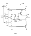
- FIG. 1 is a schematic diagram of a non-inverting domino register implemented according to a prior disclosure which is incorporated by reference;
- FIG. 3 is a schematic diagram of a footless non-inverting domino register implemented according to an exemplary embodiment of the present invention
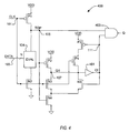
- FIG. 4 is a schematic diagram of another non-inverting domino register implemented according to an exemplary embodiment of the present invention employing an improved storage stage;
- FIG. 8 is a schematic diagram of a P-domino circuit according to another exemplary embodiment of the present invention.
- FIG. 1 is a schematic diagram of a non-inverting domino register 100 implemented according to the prior disclosure CNTR.2200.
- the non-inverting domino register 100 includes a logic evaluation input stage, or domino stage, which consists of stacked P-channel and N-channel devices P1 and N2 and evaluation logic 104.
- the P1 and N2 devices are a complementary pair of evaluation devices coupled on either side of evaluation logic 104 in the stack.
- the evaluation logic 104 may be as simple as a single N-channel device or may be significantly more complex for evaluation any desired logic function.
- the source of P1 is coupled to a voltage source VDD and its drain is coupled to node 105 providing a signal TOP.
- TOP When the evaluation logic "fails to evaluate,” TOP remains at its pre-charged high state. At time T0 when the CLK signal is initially low, N2 is turned off and P 1 is turned on, so that the domino stage pre-charges the TOP signal high.
- the TOP signal is pre-charged high in preparation for evaluation of the DATA N signal by the evaluation logic 104 upon the rising edge of CLK, where the DATA N signal is initially high.
- the pre-charged TOP signal turns on N4 and N6.
- the QII signal remains at its former state (shown initially in a low logic state) and is held there by the keeper circuit 109.
- the QI signal is initially high turning on N5, so that the Q output signal is initially pulled low via the N5 and N6 devices.
- the TOP signal is once again pre-charged high.
- P2 and N3 are turned off so that node 107 is not driven to either state.
- the respective states of the QII and QI signals remain unchanged, however, via operation of the keeper circuit 109, so that the Q and QII signals remain high and the QI signal remains low throughout the remainder of the half cycle of CLK.
- one embodiment of the present invention employs ratioed P and N devices to configure the evaluation logic.
- strong N devices and weak P devices are employed, resulting in faster operation.
- FIG. 3 is a schematic diagram of another non-inverting domino register 300 implemented according to an exemplary embodiment of the present invention.
- the non-inverting domino register 300 is substantially similar to the non-inverting domino register 100 except that the logic evaluation input stage, or domino stage, comprising the stacked P-channel and N-channel devices P1 and N2 and evaluation logic .104, is reordered into a "footless" configuration and the evaluation logic 104 is replaced with evaluation logic 301.
- the P1 and N2 devices are a complementary pair of evaluation devices coupled together at the node 105 providing the TOP signal. In this case, the drain of N2 is coupled to node 105 and its source is coupled to the top or upper end of the evaluation logic 301.
- the lower or bottom end of the evaluation logic 301 is coupled to ground. In this manner, the evaluation logic 301 is located at the foot of the P1/N2 stack as opposed to being coupled between P1 and N2. Operation is substantially similar and the timing diagram of FIG. 2 remains equally valid for the non-inverting domino register 300.
- the evaluation logic 301 could be configured in substantially the same manner as the evaluation logic 104. As understood by those skilled in the art, however, the evaluation logic 301 may alternatively be embodied using complementary metal-oxide semiconductor (CMOS) logic rather than N-channel logic, where again, the timing diagram of FIG. 2 remains valid.
- CMOS logic provides significantly better input level noise margin over N-channel logic so that the non-inverting domino register 300 provides significantly better input level noise margin over the non-inverting domino register 100 when using CMOS logic in the domino stage.
- FIG. 4 is a schematic diagram of another non-inverting domino register 400 implemented according to an exemplary embodiment of the present invention employing an improved keeper circuit.
- the non-inverting domino register 400 includes an input domino stage followed by a storage stage and an output stage.
- the domino stage and the initial portion of the storage stage of the register 400 are similar to those of the register 100.
- the keeper circuit of the register 400 is modified to improve performance by eliminating the need to overcome devices and reduce cost in terms of speed and current.
- the domino stage includes stacked P-channel and N-channel devices P1 and N2 and evaluation logic 104.
- the P1 and N2 devices are a complementary pair of evaluation devices coupled on either side of evaluation logic 104 between the voltage source VDD and ground.
- the source of P1 is coupled to VDD and its drain is coupled to node 105 providing the TOP signal.
- the evaluation logic 104 is coupled between node 105 and the drain of N2 and the source of N2 is coupled to ground.
- the input clock signal CLK is provided via node 101 to the gates of P1, N2 and N3.
- a set of N nodes 103 provide N input data signals DATA to the evaluation logic 104.
- the node 105 providing the TOP signal is coupled to the gates of devices P2 and N4.
- the initial portion of the storage stage is substantially the same write stage including the stacked devices P2, N3 and N4.
- the source of P2 is coupled to VDD and its drain is coupled to node 107 developing the first intermediate output signal QII.
- the drain of N3 is coupled to node 107 and its source is coupled to the drain of N4, having its source coupled to ground.
- Node 107 developing the QII signal, is coupled to the input of the inverter 401, having its output coupled to node 111 developing the second intermediate output signal QI.
- Node 111 is coupled to the gates of P3 and N5 and is coupled to one input of the NAND gate 403.
- the timing diagram of FIG. 2 is applicable for the non-inverting domino register 400 for this situation with only minor differences in timing, where such timing differences and small delays are ignored (e.g., delays through the inverter 401 and the NAND gate 403 are ignored).
- the QII signal is initially low and is to be asserted high.
- the CLK, Q and QII signals are initially low and the QI signal is high. Since CLK is low, P1 is turned on and TOP is pre-charged high turning on N4. Since QI and TOP are both high, the Q signal at the output of the NAND gate 403 is initially low. While CLK is low and QI is high, N5 is on, P3 is off, and P4 is on.
- the low keeper path through N5 is disabled because N4 is turned off when the TOP signal goes low. And since N4 is turned off, P2 does not have to overcome N5 to pull the QII signal high. Whenever the QII signal is low and is to be pulled high in response to evaluation (pulling TOP low), the low keeper path is always disabled (because N4 is off) so that the write stage of the storage stage does not have to overcome a keeper device.
- FIG. 5 is a schematic diagram of another footless non-inverting domino register 500 employing the improved keeper stage of the register 400 and implemented according to another exemplary embodiment of the present invention.
- the non-inverting domino register 500 is substantially similar to the non-inverting domino register 400, except that the logic evaluation input stage, or domino stage, comprising the stacked P-channel and N-channel devices P 1 and N2 and evaluation logic 104, is reordered into a "footless" configuration and the evaluation logic 104 is replaced with evaluation logic 301.
- the change from register 500 from 400 is analogous to the change from register 300 to 100.
- the evaluation logic 301 of the non-inverting domino register 500 may be implemented with CMOS logic rather than N-channel logic, where again, the timing diagram of FIG. 2 remains applicable.
- CMOS logic provides significantly better input level noise margin over N-channel logic so that the non-inverting domino register 500 provides somewhat better input level noise margin over the non-inverting domino register 400 when using CMOS logic in the domino stage.
- a non-inverting domino register implemented according to an embodiment of the present invention has a faster clock-to-output time than conventional approaches without compromising the stability of its output, Q.
- the storage stage may further be improved to allow for smaller, faster devices to be employed in a high leakage environment than those which would otherwise be required to overcome strong keeper devices.
- This enables the non-inverting domino register to be embodied in a high leakage or high noise process, such as 90 nm SOI and the like, without causing performance degradation caused by leakage factors.
- the benefits of a scaled process including reduced size, voltage, power consumption, etc., may be attained without causing the performance degradation associated with such scaled processes.
- the CLK signal goes high, which causes the TOP signal to discharge low since the DATA N signal is high.
- N2 is turned on and the evaluation logic 104 evaluates pulling TOP low via N2 to ground.
- the QII signal is pulled high via P2 and the Q output signal is pulled high via P4.
- the QII and Q signals are both pulled high at about the same time T1, and the QI signal is pulled low by the inverter 109A.
- the inverted state of the QI signal at the output of the keeper circuit 109 drives the devices P3 and N5. When QI is high, P3 is off and N5 is on; and when QI is low, P3 is on and N5 is off.
- the TOP signal is once again pre-charged high.
- P2 and N3 are turned off so that node 107 is not driven to either state.
- the respective states of the QII and QI signals remain unchanged, however, via operation of the keeper circuit 109, so that the Q and QII signals remain high and the QI signal remains low throughout the remainder of the half cycle of CLK.
- the DATA N is shown going low at time T3 while the CLK signal is still low, and the CLK signal is next asserted high at time T4 while the DATA N signal is low.
- the evaluation logic 104 fails to evaluate, so that TOP remains high while CLK is high.
- the CLK and TOP signals turn on devices N3 and N4, respectively, so that the QII signal is asserted low at about time T4, and the QI signal is consequently pulled high by the inverter 109A.
- the TOP signal being high keeps N6 on.
- the QI signal turns N5 on and P3 off, so that the Q signal is pulled low via N5 and N6.
- the CLK signal next goes low at time T5 pulling TOP high again.
- the respective states of the QII and QI signals remain unchanged via operation of the keeper circuit 109.
- the Q signal remains low throughout the remainder of the cycle of CLK since QI keeps N5 on and TOP keeps N6 on.
- non-inverting domino register 100 transitions of the output Q signal of the non-inverting domino register 100 are very fast in response to transitions of the CLK signal. If a non-inverting output is necessary or otherwise desired, the non-inverting domino register 100 provides superior data-to-output speed compared to conventional designs among other benefits and advantages.
- the non-inverting domino register 100 may be converted to an inverting domino register simply by adding an output inverter/buffer (not shown).
- the only difference between the timing diagram of FIGURE 2 and the timing diagram of FIGURE 6 is that node 103 of the non-inverting domino registers of FIGURES 1, 3, 4, and 5 are each coupled to a pulsed clock signal CLK rather than being coupled to an approximately symmetric clock signal CLK. Accordingly, the hold time requirement for data signal DATA N is reduced significantly over the embodiments discussed with reference to FIGURE 2.
- the duty cycle of the pulsed clock signal CLK is less than or equal to 10 percent.
- the time from T1 (when CLK goes high) until T3 (when the state of DATA N is allowed to change) is markedly less than the comparable period of FIGURE 2. Such an embodiment of the present invention is preferred for minimizing hold time.
- the previous state (i.e., the state prior to CLK going low) of DATA N is latched through signals QII, QI, and through to the output Q.
- CLK goes back high, opening up a window in which the state of DATA N is allowed to propagate though to the output Q. Since DATA N is low, the output Q remains low.
- DATAN goes high causing signal TOP to discharge, thus turning on P2 and causing the output Q to go high.
- CLK goes back low, closing the evaluation window and latching the state of DATA N , thus keeping Q high during this period.
- DATA N also goes back low at T3, reflecting the state of a preceding domino stage whose output is coupled to node 803.
- FIG. 8 a schematic diagram is presented of a P-domino circuit 800 according to the present invention.
- the P-domino circuit 800 may be employed as either a latch or a register exhibiting advantages over the prior art as will be described in detail with reference to the timing diagrams of FIGURES 9 and 10.
- the present inventors have also recognized the need to solve the problem of slow clock-to-output times on P-domino output latches and registers. They have therefore developed a P-domino output circuit 800 that may be employed as either a latch or a register, based upon the type of clock signal and data inputs to which the P-domino circuit 800 is coupled.
- the P-domino circuit 800 includes three stages, including an evaluation stage, a latching stage, and an output stage.
- the evaluation stage is formed by a P-channel device P1, an N-channel device N1 and an inverter U1.
- the latching stage is formed by P-channel devices P2 and P3 and an N-channel device N2 coupled in a stack configuration.
- the output stage is formed by a P-channel device P4, N-channel devices N3 and N4, inverter U2, and a two-input NOR gate U3.
- PH1B has a duty cycle less than or equal to 10 percent.
- the QIIB signal is initially high and is to be asserted low in response to the PH1B signal going low since the DB signal is low. Also at time T0, the PH1B signal is initially high while the QIB signal is low. Since PH1B is high, N1 is turned on and TOPB is "pre-charged" low so that P2 and N3 are both turned on. Since QIB and TOPB are both low, the QB signal at the output of the NOR gate U3 is initially high. While PH1B is high and QIB is low, N4 is off, N3 is on and P4 is on. In this case, therefore, P4 and N3 are both on providing a "high" state keeper path for the node 807 to VDD which keeps the QIIB signal high.
- the DB signal goes high at time T3 to set up for the next edge of PH1B so that the inverter U1 pulls the source of P1 low.
- the PH1B signal next goes low at time T4 turning P1 on. Since DB is still high and the source of P1 is low, TOPB remains low at time T4.
- the PH1B signal going low turns N3 off and P3 on. Since N2 remains off and P2 and P3 are both turned on, the QIIB signal is pulled high.
- the inverter U2 pulls QIB low in response to QIIB going high. Since QIB and TOPB are now both low, the NOR gate U3 pulls QB high.
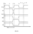
- FIGURE 10 a timing diagram is presented illustrating a P-domino latch embodiment of the present invention.
- the latch clock signal PH1B exhibits from a 40 percent to a 60 percent duty cycle.
- DB also goes back high at T3, reflecting the state of a preceding domino stage whose output is coupled to node 803.
- TOPB precharges low at time T3, setting up for the next evaluation window when PH1B goes low at time T4. Since DB is high at time T4, TOP does not discharge. Thus at time T4, P2 and P3 are on, driving QIIB high and QIB low. Because both QIB and TOPB are low at T4, QB is driven high.
- TOPB remains low and the high state remains at the output QB.
- PH1B goes back high , latching in the state of DB at the output QB during the period when PH1B is low.
Landscapes
- Engineering & Computer Science (AREA)
- Power Engineering (AREA)
- Physics & Mathematics (AREA)
- Computer Hardware Design (AREA)
- Computing Systems (AREA)
- General Engineering & Computer Science (AREA)
- Mathematical Physics (AREA)
- Logic Circuits (AREA)
Applications Claiming Priority (2)
| Application Number | Priority Date | Filing Date | Title |
|---|---|---|---|
| US11/023,145 US7187209B2 (en) | 2003-08-13 | 2004-12-27 | Non-inverting domino register |
| US11/251,517 US7417465B2 (en) | 2002-08-14 | 2005-10-14 | N-domino output latch |
Publications (3)
| Publication Number | Publication Date |
|---|---|
| EP1732227A2 true EP1732227A2 (de) | 2006-12-13 |
| EP1732227A3 EP1732227A3 (de) | 2009-03-04 |
| EP1732227B1 EP1732227B1 (de) | 2011-08-24 |
Family
ID=36084438
Family Applications (1)
| Application Number | Title | Priority Date | Filing Date |
|---|---|---|---|
| EP05257036A Expired - Lifetime EP1732227B1 (de) | 2004-12-27 | 2005-11-15 | N-Domino Kippschaltung |
Country Status (3)
| Country | Link |
|---|---|
| US (1) | US7417465B2 (de) |
| EP (1) | EP1732227B1 (de) |
| ES (1) | ES2370828T3 (de) |
Families Citing this family (8)
| Publication number | Priority date | Publication date | Assignee | Title |
|---|---|---|---|---|
| US7358775B2 (en) * | 2005-01-14 | 2008-04-15 | Via Technologies, Inc. | Inverting dynamic register with data-dependent hold time reduction mechanism |
| US7317339B1 (en) * | 2006-06-16 | 2008-01-08 | Via Technologies, Inc. | N-domino register with accelerated non-discharge path |
| US7348806B2 (en) * | 2006-08-11 | 2008-03-25 | Via Technologies, Inc. | Accelerated N-channel dynamic register |
| US7990180B2 (en) * | 2009-09-09 | 2011-08-02 | Via Technologies, Inc. | Fast dynamic register |
| RU2427073C1 (ru) * | 2010-05-24 | 2011-08-20 | Учреждение Российской академии наук Институт проблем управления им. В.А. Трапезникова РАН | Тактируемый логический элемент |
| US8928377B2 (en) | 2013-04-24 | 2015-01-06 | Via Technologies, Inc. | Scannable fast dynamic register |
| US10331196B2 (en) | 2017-06-19 | 2019-06-25 | Advanced Micro Devices, Inc. | Reduced setup time clock gating circuit |
| CN112100793B (zh) | 2019-05-31 | 2023-06-13 | 超威半导体(上海)有限公司 | 用于重定时流水线的基于条带的自选通 |
Citations (2)
| Publication number | Priority date | Publication date | Assignee | Title |
|---|---|---|---|---|
| US20040257115A1 (en) | 2003-04-28 | 2004-12-23 | Via Technologies, Inc. | N-domino output latch with accelerated evaluate path |
| US20050046446A1 (en) | 2003-08-27 | 2005-03-03 | Via Technologies Inc. | Dynamic logic register |
Family Cites Families (13)
| Publication number | Priority date | Publication date | Assignee | Title |
|---|---|---|---|---|
| US5075386A (en) * | 1990-04-12 | 1991-12-24 | Eastman Kodak Company | Cross-linkable hot-melt adhesive and method of producing same |
| US5889979A (en) * | 1996-05-24 | 1999-03-30 | Hewlett-Packard, Co. | Transparent data-triggered pipeline latch |
| US5926038A (en) * | 1997-11-10 | 1999-07-20 | The United States Of America As Represented By The Secretary Of The Navy | Two-phase dynamic logic circuits for gallium arsenide complementary HIGFET fabrication |
| US6265899B1 (en) * | 1999-06-04 | 2001-07-24 | S3 Incorporated | Single rail domino logic for four-phase clocking scheme |
| US6191618B1 (en) * | 1999-07-23 | 2001-02-20 | Intel Corporation | Contention-free, low clock load domino circuit topology |
| US6560737B1 (en) * | 2000-02-16 | 2003-05-06 | Hewlett-Packard Development Company, L.P. | Method for adding scan controllability and observability to domino CMOS with low area and delay overhead |
| US6496038B1 (en) * | 2000-06-30 | 2002-12-17 | Intel Corporation | Pulsed circuit topology including a pulsed, domino flip-flop |
| US6498514B2 (en) * | 2001-04-30 | 2002-12-24 | Intel Corporation | Domino circuit |
| US6956406B2 (en) * | 2001-07-02 | 2005-10-18 | Intrinsity, Inc. | Static storage element for dynamic logic |
| GB0121013D0 (en) * | 2001-08-30 | 2001-10-24 | Micron Technology Inc | Combined dynamic logic gate and level shifter and method employing same |
| US6628143B2 (en) * | 2001-09-26 | 2003-09-30 | Intel Corporation | Full-swing source-follower leakage tolerant dynamic logic |
| US6650145B2 (en) * | 2002-04-04 | 2003-11-18 | International Business Machines Corporation | Circuits and systems for limited switch dynamic logic |
| US20050110522A1 (en) * | 2003-11-21 | 2005-05-26 | Hoekstra George P. | Multistage dynamic domino circuit with internally generated delay reset clock |
-
2005
- 2005-10-14 US US11/251,517 patent/US7417465B2/en not_active Expired - Lifetime
- 2005-11-15 ES ES05257036T patent/ES2370828T3/es not_active Expired - Lifetime
- 2005-11-15 EP EP05257036A patent/EP1732227B1/de not_active Expired - Lifetime
Patent Citations (2)
| Publication number | Priority date | Publication date | Assignee | Title |
|---|---|---|---|---|
| US20040257115A1 (en) | 2003-04-28 | 2004-12-23 | Via Technologies, Inc. | N-domino output latch with accelerated evaluate path |
| US20050046446A1 (en) | 2003-08-27 | 2005-03-03 | Via Technologies Inc. | Dynamic logic register |
Also Published As
| Publication number | Publication date |
|---|---|
| EP1732227A3 (de) | 2009-03-04 |
| EP1732227B1 (de) | 2011-08-24 |
| US7417465B2 (en) | 2008-08-26 |
| ES2370828T3 (es) | 2011-12-23 |
| US20060033534A1 (en) | 2006-02-16 |
Similar Documents
| Publication | Publication Date | Title |
|---|---|---|
| US7317339B1 (en) | N-domino register with accelerated non-discharge path | |
| EP1592133B1 (de) | N-Domino Ausgangskippschaltung mit schnellem Auswertepfad | |
| US20050248368A1 (en) | P-domino output latch with accelerated evaluate path | |
| US7212039B2 (en) | Dynamic logic register | |
| EP1732227B1 (de) | N-Domino Kippschaltung | |
| EP1693964B1 (de) | P-Domino Kippschaltung | |
| US7187209B2 (en) | Non-inverting domino register | |
| EP1868292B1 (de) | Schnelle P-Domino-Registerschaltung | |
| EP1732226B1 (de) | P-Domino Datenregister | |
| EP1887699B1 (de) | Beschleunigtes dynamisches N-Kanal Register | |
| US7193445B2 (en) | Non-inverting domino register | |
| EP1887692B1 (de) | Dynamisches Register mit beschleunigtem P-Kanal | |
| US20040113658A1 (en) | Dynamic logic register | |
| US20050055538A1 (en) | Dynamic logic return-to-zero latching mechanism | |
| CN100395698C (zh) | 非反相骨牌缓存器 | |
| CN100550639C (zh) | 多米诺输出锁存器 | |
| CN1738206B (zh) | 非反相多米诺寄存器和产生非反相输出的方法 | |
| EP1542364B1 (de) | Dynamisches logisches Register |
Legal Events
| Date | Code | Title | Description |
|---|---|---|---|
| PUAI | Public reference made under article 153(3) epc to a published international application that has entered the european phase |
Free format text: ORIGINAL CODE: 0009012 |
|
| AK | Designated contracting states |
Kind code of ref document: A2 Designated state(s): AT BE BG CH CY CZ DE DK EE ES FI FR GB GR HU IE IS IT LI LT LU LV MC NL PL PT RO SE SI SK TR |
|
| AX | Request for extension of the european patent |
Extension state: AL BA HR MK YU |
|
| PUAL | Search report despatched |
Free format text: ORIGINAL CODE: 0009013 |
|
| AK | Designated contracting states |
Kind code of ref document: A3 Designated state(s): AT BE BG CH CY CZ DE DK EE ES FI FR GB GR HU IE IS IT LI LT LU LV MC NL PL PT RO SE SI SK TR |
|
| AX | Request for extension of the european patent |
Extension state: AL BA HR MK YU |
|
| 17P | Request for examination filed |
Effective date: 20090429 |
|
| 17Q | First examination report despatched |
Effective date: 20090528 |
|
| AKX | Designation fees paid |
Designated state(s): DE ES FR GB |
|
| GRAP | Despatch of communication of intention to grant a patent |
Free format text: ORIGINAL CODE: EPIDOSNIGR1 |
|
| GRAS | Grant fee paid |
Free format text: ORIGINAL CODE: EPIDOSNIGR3 |
|
| GRAA | (expected) grant |
Free format text: ORIGINAL CODE: 0009210 |
|
| AK | Designated contracting states |
Kind code of ref document: B1 Designated state(s): DE ES FR GB |
|
| REG | Reference to a national code |
Ref country code: GB Ref legal event code: FG4D |
|
| REG | Reference to a national code |
Ref country code: DE Ref legal event code: R096 Ref document number: 602005029691 Country of ref document: DE Effective date: 20111020 |
|
| REG | Reference to a national code |
Ref country code: ES Ref legal event code: FG2A Ref document number: 2370828 Country of ref document: ES Kind code of ref document: T3 Effective date: 20111223 |
|
| PLBE | No opposition filed within time limit |
Free format text: ORIGINAL CODE: 0009261 |
|
| STAA | Information on the status of an ep patent application or granted ep patent |
Free format text: STATUS: NO OPPOSITION FILED WITHIN TIME LIMIT |
|
| 26N | No opposition filed |
Effective date: 20120525 |
|
| REG | Reference to a national code |
Ref country code: DE Ref legal event code: R097 Ref document number: 602005029691 Country of ref document: DE Effective date: 20120525 |
|
| REG | Reference to a national code |
Ref country code: FR Ref legal event code: PLFP Year of fee payment: 11 |
|
| REG | Reference to a national code |
Ref country code: FR Ref legal event code: PLFP Year of fee payment: 12 |
|
| REG | Reference to a national code |
Ref country code: FR Ref legal event code: PLFP Year of fee payment: 13 |
|
| REG | Reference to a national code |
Ref country code: FR Ref legal event code: PLFP Year of fee payment: 14 |
|
| REG | Reference to a national code |
Ref country code: DE Ref legal event code: R082 Ref document number: 602005029691 Country of ref document: DE Representative=s name: HL KEMPNER PATENTANWAELTE, SOLICITORS (ENGLAND, DE Ref country code: DE Ref legal event code: R082 Ref document number: 602005029691 Country of ref document: DE Representative=s name: HL KEMPNER PATENTANWALT, RECHTSANWALT, SOLICIT, DE Ref country code: DE Ref legal event code: R082 Ref document number: 602005029691 Country of ref document: DE Representative=s name: HL KEMPNER PARTG MBB, DE |
|
| PGFP | Annual fee paid to national office [announced via postgrant information from national office to epo] |
Ref country code: DE Payment date: 20241126 Year of fee payment: 20 |
|
| PGFP | Annual fee paid to national office [announced via postgrant information from national office to epo] |
Ref country code: GB Payment date: 20241023 Year of fee payment: 20 |
|
| PGFP | Annual fee paid to national office [announced via postgrant information from national office to epo] |
Ref country code: FR Payment date: 20241023 Year of fee payment: 20 |
|
| PGFP | Annual fee paid to national office [announced via postgrant information from national office to epo] |
Ref country code: ES Payment date: 20241204 Year of fee payment: 20 |
|
| REG | Reference to a national code |
Ref country code: DE Ref legal event code: R071 Ref document number: 602005029691 Country of ref document: DE |
|
| REG | Reference to a national code |
Ref country code: ES Ref legal event code: FD2A Effective date: 20251127 |
|
| REG | Reference to a national code |
Ref country code: GB Ref legal event code: PE20 Expiry date: 20251114 |
|
| PG25 | Lapsed in a contracting state [announced via postgrant information from national office to epo] |
Ref country code: ES Free format text: LAPSE BECAUSE OF EXPIRATION OF PROTECTION Effective date: 20251116 |