EP1730574B1 - Electrowetting display element - Google Patents
Electrowetting display element Download PDFInfo
- Publication number
- EP1730574B1 EP1730574B1 EP05729433A EP05729433A EP1730574B1 EP 1730574 B1 EP1730574 B1 EP 1730574B1 EP 05729433 A EP05729433 A EP 05729433A EP 05729433 A EP05729433 A EP 05729433A EP 1730574 B1 EP1730574 B1 EP 1730574B1
- Authority
- EP
- European Patent Office
- Prior art keywords
- liquid
- layer
- conductive
- display element
- particles
- Prior art date
- Legal status (The legal status is an assumption and is not a legal conclusion. Google has not performed a legal analysis and makes no representation as to the accuracy of the status listed.)
- Ceased
Links
- 239000007788 liquid Substances 0.000 claims abstract description 110
- 239000002245 particle Substances 0.000 claims abstract description 62
- 239000010410 layer Substances 0.000 claims description 190
- 239000000463 material Substances 0.000 claims description 17
- 239000011148 porous material Substances 0.000 claims description 7
- 239000013545 self-assembled monolayer Substances 0.000 claims description 5
- 239000011159 matrix material Substances 0.000 claims description 4
- 239000002094 self assembled monolayer Substances 0.000 claims description 4
- 239000004038 photonic crystal Substances 0.000 claims description 3
- 239000004811 fluoropolymer Substances 0.000 claims description 2
- 229920002313 fluoropolymer Polymers 0.000 claims description 2
- 239000002608 ionic liquid Substances 0.000 claims description 2
- 150000002500 ions Chemical class 0.000 claims description 2
- 239000000049 pigment Substances 0.000 claims description 2
- 229920000867 polyelectrolyte Polymers 0.000 claims description 2
- 229920000642 polymer Polymers 0.000 claims description 2
- 239000002904 solvent Substances 0.000 claims description 2
- 239000000549 coloured material Substances 0.000 claims 1
- 239000010954 inorganic particle Substances 0.000 claims 1
- 239000011146 organic particle Substances 0.000 claims 1
- 239000004020 conductor Substances 0.000 description 24
- 239000000758 substrate Substances 0.000 description 14
- 238000000576 coating method Methods 0.000 description 9
- VYPSYNLAJGMNEJ-UHFFFAOYSA-N Silicium dioxide Chemical compound O=[Si]=O VYPSYNLAJGMNEJ-UHFFFAOYSA-N 0.000 description 8
- 230000005499 meniscus Effects 0.000 description 7
- 230000000694 effects Effects 0.000 description 6
- 239000012530 fluid Substances 0.000 description 5
- 239000011248 coating agent Substances 0.000 description 4
- 238000004519 manufacturing process Methods 0.000 description 4
- 239000000377 silicon dioxide Substances 0.000 description 4
- 238000000034 method Methods 0.000 description 3
- BQCADISMDOOEFD-UHFFFAOYSA-N Silver Chemical compound [Ag] BQCADISMDOOEFD-UHFFFAOYSA-N 0.000 description 2
- 239000011258 core-shell material Substances 0.000 description 2
- 239000013078 crystal Substances 0.000 description 2
- 239000002923 metal particle Substances 0.000 description 2
- 239000011022 opal Substances 0.000 description 2
- 230000003287 optical effect Effects 0.000 description 2
- 229910052709 silver Inorganic materials 0.000 description 2
- 239000004332 silver Substances 0.000 description 2
- 239000007787 solid Substances 0.000 description 2
- 239000012780 transparent material Substances 0.000 description 2
- XLYOFNOQVPJJNP-UHFFFAOYSA-N water Substances O XLYOFNOQVPJJNP-UHFFFAOYSA-N 0.000 description 2
- RICKKZXCGCSLIU-UHFFFAOYSA-N 2-[2-[carboxymethyl-[[3-hydroxy-5-(hydroxymethyl)-2-methylpyridin-4-yl]methyl]amino]ethyl-[[3-hydroxy-5-(hydroxymethyl)-2-methylpyridin-4-yl]methyl]amino]acetic acid Chemical compound CC1=NC=C(CO)C(CN(CCN(CC(O)=O)CC=2C(=C(C)N=CC=2CO)O)CC(O)=O)=C1O RICKKZXCGCSLIU-UHFFFAOYSA-N 0.000 description 1
- LSDPWZHWYPCBBB-UHFFFAOYSA-N Methanethiol Chemical compound SC LSDPWZHWYPCBBB-UHFFFAOYSA-N 0.000 description 1
- 230000008901 benefit Effects 0.000 description 1
- 230000008859 change Effects 0.000 description 1
- 238000010276 construction Methods 0.000 description 1
- 230000007423 decrease Effects 0.000 description 1
- 239000012777 electrically insulating material Substances 0.000 description 1
- 238000005516 engineering process Methods 0.000 description 1
- 238000003384 imaging method Methods 0.000 description 1
- 239000012212 insulator Substances 0.000 description 1
- 238000003475 lamination Methods 0.000 description 1
- 230000007246 mechanism Effects 0.000 description 1
- 230000001404 mediated effect Effects 0.000 description 1
- 229910052751 metal Inorganic materials 0.000 description 1
- 239000002184 metal Substances 0.000 description 1
- 230000004048 modification Effects 0.000 description 1
- 238000012986 modification Methods 0.000 description 1
- 239000002078 nanoshell Substances 0.000 description 1
- 230000000149 penetrating effect Effects 0.000 description 1
- 238000002360 preparation method Methods 0.000 description 1
- 238000007639 printing Methods 0.000 description 1
- 230000008707 rearrangement Effects 0.000 description 1
- 238000002310 reflectometry Methods 0.000 description 1
- 238000007789 sealing Methods 0.000 description 1
- 239000002356 single layer Substances 0.000 description 1
Images


Classifications
-
- G—PHYSICS
- G02—OPTICS
- G02B—OPTICAL ELEMENTS, SYSTEMS OR APPARATUS
- G02B26/00—Optical devices or arrangements for the control of light using movable or deformable optical elements
- G02B26/004—Optical devices or arrangements for the control of light using movable or deformable optical elements based on a displacement or a deformation of a fluid
-
- B—PERFORMING OPERATIONS; TRANSPORTING
- B82—NANOTECHNOLOGY
- B82Y—SPECIFIC USES OR APPLICATIONS OF NANOSTRUCTURES; MEASUREMENT OR ANALYSIS OF NANOSTRUCTURES; MANUFACTURE OR TREATMENT OF NANOSTRUCTURES
- B82Y30/00—Nanotechnology for materials or surface science, e.g. nanocomposites
Definitions
- This invention relates to the field of display elements, in particular to the field of passive display elements.
- Display elements can be either active, i.e. emit light such as LED, OLED, PLED, EL, or passive, i.e. affect the passage, reflection or refraction of light such as LCD, CLC, e-ink etc..
- Some passive systems are bistable such they can be switched and remain switched after the power has been removed.
- Most configurations previously disclosed can be readily adapted to colour functionality.
- US6473492 discloses a fluid element device that rearranges fluid within a capillary tube. A voltage is used to move the fluid within the capillary to a desired level.
- US2002/0080920 discloses a filter device using an array of elements based upon US6473492 for use with X-ray imaging equipment.
- US2003/0085850 discloses an electrostatic device that changes a meniscus shape such that the focal length of the device changes.
- US6449081 describes a focussing element based on the electrowetting phenomenon.
- WO2/002099527 describes a display element with a defined prismatic structure that contains two immiscible fluids together with electrodes such that the fluid can be rearranged with the cell.
- the display element is capacitative in nature and thus has low power consumption and is switched by low voltages.
- the element modifies the reflectivity of the surface thereof.
- a display element comprising at least two conductive porous layers and a conductive liquid, the conductive porous layers comprising a plurality of connected conductive particles insulated from the conductive liquid by a dielectric and lyophobic covering, and means for separately connecting a voltage across the at least two porous layers and the liquid such that on sequential application of a voltage to each conductive layer the liquid is displaced from one location to another location, the liquid only returning to the original location upon alternate sequential application of a voltage.
- At least one further layer is provided adjacent to the at least two conductive porous layers, the liquid having a contact angle with the material of the further layer of less than 60°, the thickness of the further layer being greater than the thickness of each conductive porous layer but less than the combined thickness of the two conductive porous layers.
- the invention further provides a device comprising at least one display element as described above including means for connection of each element to a circuit to create a matrix display.
- the present invention is simple to manufacture over large areas because of the stochastic structure of the elements and may be manufactured via roll-to-roll techniques. It fulfils the requirement of capturing small liquid elements by capillarity. However the switching time of the element is not limited by its area. It is also simple to address and drive, via suitably patterned passive or active matrix type backplanes.
- the bi-stable nature of the element allows the device to remain in one state until power is supplied to switch the element to another state.
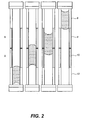
- Figure 1 is a schematic view of a display element according to the invention.
- the invention relates to a passive display element.
- upper defines the side from which an element would be viewed.
- lower defines the side opposite the upper side.
- upper and lower are not to be taken as limiting the orientation of the element according to the invention in any way.
- the element illustrated in Figure 1 is based upon a four layer porous system.
- the layers, 6, 8, 10 and 12 are located one above another with layer 6 being at the top. Between each layer there is provided a conductor 14 for connection to the liquid.
- the conductors may comprise wire filaments.
- Further conductors 20 and 22 are provided in connection with layer 8 and layer 10 respectively.
- the element is encapsulated by an upper substrate 24 and a lower substrate 26.
- the substrates may be flexible and conductive.
- the upper substrate must be of a transparent material.
- the upper layer 6 comprises a plurality of particles 28, such as silica.
- silica is only an example of the material which can be used. Any other lyophilic material may be used that can be matched with the refractive index of the liquid used.
- the particle sizes would be in the order of 30nm to 2 ⁇ m.
- a liquid 18 resides in the pore space of the upper layer 6.
- the liquid may be water but it will be understood by those skilled in the art that it is not essential that the liquid is water. However the liquid must be conductive.
- the conductive liquid may be created by adding ions to a solvent. Alternatively the conductive liquid may be an ionic liquid.
- the refractive index of the particles 28 in the upper layer 6 should be substantially the same as the refractive index of the liquid 18.
- the size of the particles 28 should be a substantial fraction of the wavelength of light, e.g. 200nm. As the refractive index of the liquid is substantially similar to that of the particles the upper layer will effectively be invisible.
- Layer 8 comprises a plurality of particles 30.
- the particles 30 should be of similar size or smaller than the particles 28 in the upper layer 6.
- the particles may be coloured to provide a coloured pixel or they may be black to provide a black pixel.
- an intermediate layer 50 of coloured or black particles may be provided between the upper layer 6 and the layer 8.
- the particles of this intermediate layer have substantially the same properties, in terms of material, size, shape etc as the particles of the upper layer 6 with the exception that they are coloured. If such an intermediate layer is used it does not matter what colour the particles of the layer 8 are as they will not be seen.
- a further option would be to use a coloured liquid 18.
- the liquid may be coloured by the addition of a dye or pigment.
- a conductor 20 is in connection with layer 8.
- the liquid 18 has a contact angle greater than 90° with the particles 30.
- the particles 30 are conductive.
- the particles may be solid metal particles or only the shell thereof may be conductive. If the particles have a shell the thickness of the shell can be chosen to create a particular coloured particle. An explanation of this can be found in Seed-mediated Growth Techniques for the Preparation of a Silver Nanoshell on a Silica Sphere, Zhong-jie Jiang and Chun-yan Liu,J. Phys. Chem B 2003, 107, 12411-12415 .
- a lyophobic material should be an insulator. Suitable particles would be conductive silver particles encased with lyophobic and dielectric mercaptan. It will be understood by those skilled in the art that this is an example only and any conductive material and lyophobic dielectric covering could be used within the terms of the invention.
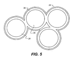
- Figure 5 illustrates a possible core shell arrangement of the particles.
- the core 26 may be a cheap insulating particle such as silica.
- a metal shell 36 encapsulates each core 26.
- the layer of lyophobic material 24 surrounds the shelled particles.
- the layer 24 may be made of, for example, polymer. Other materials that may be used include a polyelectrolyte, a fluoropolymer, a self assembled monolayer, SAM, or an inorganic shell. However the invention is not to be taken as limited to these materials.
- the metallic component of the particles 30 in the layer 6 should be connected and the lyophobic covering 24 completely encapsulate the structure.
- Layer 10 comprises a plurality of particles 32.
- the particles 32 are substantially the same as the particles 30 in layer 8.
- the liquid 18 has a contact angle greater that 90° with the particles 32.
- the particles are conductive with a thin covering of lyophobic material as described above.
- a conductor 22 is in connection with layer 10.
- the lowermost layer 12 comprises a plurality of particles 34.
- the particles may comprise any lyophilic material.
- the particles should be substantially similar to those in layer 6 in terms of contact angle with the liquid, size, etc..
- the particle sizes would be in the order of 30nm to 2 ⁇ m.
- the volume of liquid 18 must be greater than or equal to the volume available in the upper layer 6 or in the lower layer 12.
- the available volume will therefore be the thickness x the area x porosity.
- the "porous thickness" of the layers 6, 8, 10 and 12 can be defined by their actual (mechanical) thickness multiplied by the porosity of the material.
- the term "thickness” as used in the description and claims of this application should be interpreted as the "porous thickness” as defined above.
- Each layer 8, 10 has a thickness less than that of layer 6 or 12. However the thickness of layers 8 and 10 combined is greater than that of layer 6 or 12 alone.
- the liquid 18 has a contact angle greater than 90° with the particles 30 in the layer 8. Therefore the capillary pressure in layer 8 is such that no liquid 18 will enter layer 8 from upper layer 6. Thus with no voltage applied to the element the liquid 18 resides in upper layer 6. As the liquid 18 and the particles 28 have a similar refractive index the upper layer 6 will appear essentially transparent or translucent. The particles 30 in the layer 8 scatter the light. Therefore the colour of the particles 30 in layer 8 can be seen. In the embodiment of the invention including an intermediate layer, illustrated in Figure 6, the colour of the particles forming the intermediate layer will be seen.
- Figure 2 illustrates what happens when voltage is applied to the element.
- the voltage applied is in the order of 2 volts, a maximum of 20V being envisaged.
- Electrowetting is explained in Blake et al, Langmuir 2000, 16, 2928-2935 .
- the electrowetting effect reduces the contact angle of the liquid 18 with the layer 8.
- ⁇ is the contact angle in the presence of a voltage
- ⁇ 0 is the contact angle with no voltage
- V is the voltage
- ⁇ is the dielectric constant of the lyophobic layer
- ⁇ 0 is the permittivity of free space
- ⁇ is the liquid surface tension
- d is the thickness of the lyophobic layer.
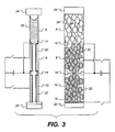
- Figure 3 illustrates an element according to a second embodiment of the invention.
- the element illustrated in Figure 3 is based upon a three layer porous system.
- the embodiment is similar in many ways to that shown in Figure 1.
- the three layers of particles are substantially the same as layers 6, 8 and 10 illustrated in Figure 1 and therefore will be labelled the same.
- a conductor 14 for connection with the liquid.
- This conductor may comprise wire filaments.
- Conductors 20 and 22 are in connection with layers 8 and 10 as described above.
- An insulating layer 16 is located below the lowest layer 12.
- the element is encapsulated by an upper substrate 24 and a lower substrate 26.
- the upper substrate must be of a transparent material.
- Each layer 8, 10 has a thickness less than that of layer 6. However the thickness of layers 8 and 10 combined is greater than that of layer 6 alone.
- the upper layer 6 may alternatively comprise a photonic crystal structure, for example, opal or reverse opal, rather than a random porous structure.
- the crystal structure acts a diffraction grating and reflects only particular wavelengths of light.
- the gaps in the crystal structure are filled with liquid the photonic nature of the layer is removed and the layer becomes transparent or translucent. Colour from the lower layer is then seen.
- the layer reflects strongly at a wavelength defined by the structure and spacing dimension of the photonic crystals.
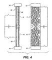
- Figure 4 illustrates an element according to a third embodiment of the invention.
- the element illustrated in Figure 4 is based upon a two layer porous system.
- the two layers of particles are substantially the same as layers 8 and 10 illustrated in Figure 1 and therefore will be labelled the same.
- the two layers 8 and 10 comprise a plurality of conductive particles.
- the particles may be solid metal particles or only the shell thereof may be conductive. Whichever type of particle is used they must be covered with a thin layer of lyophobic electrically insulating material as described above.
- the particle size and particle composition should be the same in each layer 8 and 10.
- the porous volume and pore size of each layer 8 and 10 should be the same.
- the layers have the same thickness.
- each layer 8 and 10 there are provided two electrodes 38 and 40 respectively.
- the electrodes allow a voltage to be applied to the particles in each layer.
- Insulating substrates 42 and 44 are provided at the top and bottom of the element.
- Substrate 42 must be transparent. These substrates seal the element.
- a conductive liquid 46 is forced, by use of electrostatics, into the layer 8. This is achieved by applying a voltage between the layer and the liquid, therefore increasing the capillary pressure as the contact angle of the liquid on the particle surface decreases.
- the volume of liquid imbibed into the layer is the same as the available volume in the pores of the layer 8 the upper transparent substrate is laid down, thus sealing the element.
- the element With the liquid in layer 10 the element will show the colour of the particles in layer 8 if viewed from the upper side. If lower substrate 44 were transparent and the element viewed through the lower substrate 44 the colour of the liquid will be seen. An inverse image is thus visible from either end of the element.
- Layer 8 thus becomes lyophilic and the difference in capillary pressures between layers 8 and 10 allows the liquid 46 to be drawn into layer 8, returning it to its original colour.
- the elements can be made using coating technology. Initially a substrate comprising a pattern of electrodes is prepared by means such as printing. Subsequently a coating process, either multiple single layer coatings or one or more multi-layer coatings is used to lay down the porous layers.
- the coating process chosen can be unmetered or preferably pre-metered. It is well known in the coating art to manufacture porous particulate layers through single or multi-layer coating processes.
- the layers will then be dried.
- the liquid can then be coated and since the top layer is lyophilic, the liquid will fill the upper layer without penetrating the lower layer.
- a final encapsulating layer is then provided by coating or by lamination and will contain electrodes to connect to the liquid layer.
- a matrix or plurality of elements can be assembled to form a display device.
- the elements of the display device would be environmentally sealed in order to encapsulate the liquid and prevent moisture ingression and liquid loss.
Landscapes
- Physics & Mathematics (AREA)
- Chemical & Material Sciences (AREA)
- Engineering & Computer Science (AREA)
- General Physics & Mathematics (AREA)
- Nanotechnology (AREA)
- Composite Materials (AREA)
- Condensed Matter Physics & Semiconductors (AREA)
- Materials Engineering (AREA)
- Crystallography & Structural Chemistry (AREA)
- Optics & Photonics (AREA)
- Electrochromic Elements, Electrophoresis, Or Variable Reflection Or Absorption Elements (AREA)
Applications Claiming Priority (2)
| Application Number | Priority Date | Filing Date | Title |
|---|---|---|---|
| GBGB0407641.0A GB0407641D0 (en) | 2004-04-02 | 2004-04-02 | Display element |
| PCT/GB2005/001081 WO2005096067A1 (en) | 2004-04-02 | 2005-03-22 | Electrowetting display element |
Publications (2)
| Publication Number | Publication Date |
|---|---|
| EP1730574A1 EP1730574A1 (en) | 2006-12-13 |
| EP1730574B1 true EP1730574B1 (en) | 2007-07-04 |
Family
ID=32247845
Family Applications (1)
| Application Number | Title | Priority Date | Filing Date |
|---|---|---|---|
| EP05729433A Ceased EP1730574B1 (en) | 2004-04-02 | 2005-03-22 | Electrowetting display element |
Country Status (7)
| Country | Link |
|---|---|
| US (1) | US7436576B2 (enExample) |
| EP (1) | EP1730574B1 (enExample) |
| JP (1) | JP4672005B2 (enExample) |
| CN (1) | CN1947049A (enExample) |
| DE (1) | DE602005001557T2 (enExample) |
| GB (1) | GB0407641D0 (enExample) |
| WO (1) | WO2005096067A1 (enExample) |
Families Citing this family (8)
| Publication number | Priority date | Publication date | Assignee | Title |
|---|---|---|---|---|
| WO2007113637A1 (en) * | 2006-03-31 | 2007-10-11 | Varioptic | Multi-phase liquid composition and optical lens driven by electrowetting |
| US20120044129A1 (en) * | 2009-04-30 | 2012-02-23 | Hewlett-Packard Development Company, L.P. | Reflective colour display device |
| DE102010013153A1 (de) * | 2010-03-27 | 2011-09-29 | Advanced Display Technology Ag | Mehrfarbige Anzeigevorrichtung |
| US8760760B2 (en) * | 2010-09-30 | 2014-06-24 | Reald Inc. | Cleanable coating for projection screen |
| JP6233596B2 (ja) | 2013-09-09 | 2017-11-22 | パナソニックIpマネジメント株式会社 | 反射型表示素子 |
| DE102014100871B4 (de) * | 2014-01-27 | 2016-11-17 | Karlsruher Institut für Technologie | Digitale Mikrofluidikplattform |
| US9529188B2 (en) * | 2015-03-25 | 2016-12-27 | Amazon Technologies, Inc. | Electrowetting device with multi layer support plate |
| CN108196361B (zh) * | 2017-12-08 | 2020-06-16 | 华南师范大学 | 一种双稳态电流体显示下基板及包括其的显示器件 |
Family Cites Families (13)
| Publication number | Priority date | Publication date | Assignee | Title |
|---|---|---|---|---|
| JPS5569126A (en) * | 1978-11-17 | 1980-05-24 | Matsushita Electric Ind Co Ltd | Light control unit |
| US4419663A (en) | 1979-03-14 | 1983-12-06 | Matsushita Electric Industrial Co., Ltd. | Display device |
| JPS5789725A (en) * | 1980-11-26 | 1982-06-04 | Matsushita Electric Ind Co Ltd | Display device |
| FR2548431B1 (fr) | 1983-06-30 | 1985-10-25 | Thomson Csf | Dispositif a commande electrique de deplacement de fluide |
| US5956005A (en) * | 1995-12-29 | 1999-09-21 | Xerox Corporation | Electrocapillary display sheet which utilizes an applied electric field to move a liquid inside the display sheet |
| FR2756431B1 (fr) | 1996-11-26 | 1999-02-12 | Planet Wattohm Snc | Accessoire d'immobilisation d'appareil electrique a clipsage direct |
| JPH10193784A (ja) * | 1997-01-10 | 1998-07-28 | Fuji Xerox Co Ltd | 可逆的記録媒体 |
| EP0884714A3 (en) * | 1997-06-10 | 1999-09-15 | Xerox Corporation | Electric display sheet |
| JP3831492B2 (ja) * | 1997-09-19 | 2006-10-11 | ゼロックス コーポレイション | ディスプレイ装置 |
| JP4160266B2 (ja) * | 2001-02-22 | 2008-10-01 | 株式会社リコー | 表示用材料 |
| FR2825481B1 (fr) * | 2001-05-31 | 2003-07-18 | Commissariat Energie Atomique | Structure electrochrome souple et procedes de fabrication de cette structure |
| US6700556B2 (en) * | 2001-07-26 | 2004-03-02 | Xerox Corporation | Display sheet with stacked electrode structure |
| US6920000B2 (en) | 2002-09-19 | 2005-07-19 | Hewlett-Packard Development Company, L.P. | Filter for a display system |
-
2004
- 2004-04-02 GB GBGB0407641.0A patent/GB0407641D0/en not_active Ceased
-
2005
- 2005-03-22 EP EP05729433A patent/EP1730574B1/en not_active Ceased
- 2005-03-22 JP JP2007505616A patent/JP4672005B2/ja not_active Expired - Fee Related
- 2005-03-22 WO PCT/GB2005/001081 patent/WO2005096067A1/en not_active Ceased
- 2005-03-22 US US10/586,063 patent/US7436576B2/en not_active Expired - Fee Related
- 2005-03-22 CN CN200580012134.4A patent/CN1947049A/zh active Pending
- 2005-03-22 DE DE602005001557T patent/DE602005001557T2/de not_active Expired - Lifetime
Also Published As
| Publication number | Publication date |
|---|---|
| DE602005001557D1 (de) | 2007-08-16 |
| JP4672005B2 (ja) | 2011-04-20 |
| US20070164981A1 (en) | 2007-07-19 |
| CN1947049A (zh) | 2007-04-11 |
| WO2005096067A1 (en) | 2005-10-13 |
| GB0407641D0 (en) | 2004-05-05 |
| DE602005001557T2 (de) | 2008-03-06 |
| JP2007531037A (ja) | 2007-11-01 |
| US7436576B2 (en) | 2008-10-14 |
| EP1730574A1 (en) | 2006-12-13 |
Similar Documents
| Publication | Publication Date | Title |
|---|---|---|
| JP4744757B2 (ja) | アクティブマトリクス駆動電子ディスプレイの性能を高めるための蓄電キャパシタの使用 | |
| US8723759B2 (en) | Display with light concentrating substrate | |
| JP6388956B2 (ja) | バックプレーンアセンブリのための複数層拡張電極構造 | |
| US6724519B1 (en) | Protective electrodes for electrophoretic displays | |
| US7839558B2 (en) | Electrowetting display and methods for manufacturing the same | |
| US20030214697A1 (en) | Electrophoretic electronic displays with low-index films | |
| EP1730575B1 (en) | Electrowetting display element | |
| CN102650733A (zh) | 电润湿显示单元及电润湿显示系统 | |
| JP2002533754A (ja) | 電気泳動ディスプレイの保護電極 | |
| WO2008105543A1 (en) | Electrophoretic sheet, electrophoresis apparatus, method for manufacturing an electrophoresis apparatus and electronic device | |
| EP1730574B1 (en) | Electrowetting display element | |
| US20110120749A1 (en) | Transparent conductor structure | |
| US8217869B2 (en) | Flexible display system | |
| CN101363960B (zh) | 电湿润性显示器及其制造方法 | |
| EP1730573B1 (en) | Electrowetting display element | |
| KR100922688B1 (ko) | 기공이 있는 구조체를 포함하는 전기영동 소자 및 그의제조방법 | |
| WO2008146263A2 (en) | Bistable electrowetting light valve | |
| DE102015103794B4 (de) | Leuchtvorrichtung mit einer Mikrofluidpumpe zum Verlagern von Fluid und Verfahren zum Betrieb einer solchen Leuchtvorrichtung | |
| US6980352B1 (en) | Encapsulated bichromal gyricon display | |
| TWI857562B (zh) | 包含囊封電泳介質的圖案區域之顯示器材料 | |
| US20250172847A1 (en) | Piezo-Electrophoretic Films and Displays, and Methods for Manufacturing the Same | |
| HK40069067A (zh) | 用於电光装置的可转移透光电极膜 |
Legal Events
| Date | Code | Title | Description |
|---|---|---|---|
| PUAI | Public reference made under article 153(3) epc to a published international application that has entered the european phase |
Free format text: ORIGINAL CODE: 0009012 |
|
| 17P | Request for examination filed |
Effective date: 20060802 |
|
| AK | Designated contracting states |
Kind code of ref document: A1 Designated state(s): DE GB |
|
| GRAP | Despatch of communication of intention to grant a patent |
Free format text: ORIGINAL CODE: EPIDOSNIGR1 |
|
| DAX | Request for extension of the european patent (deleted) | ||
| RBV | Designated contracting states (corrected) |
Designated state(s): DE GB |
|
| GRAS | Grant fee paid |
Free format text: ORIGINAL CODE: EPIDOSNIGR3 |
|
| GRAA | (expected) grant |
Free format text: ORIGINAL CODE: 0009210 |
|
| AK | Designated contracting states |
Kind code of ref document: B1 Designated state(s): DE GB |
|
| REG | Reference to a national code |
Ref country code: GB Ref legal event code: FG4D |
|
| REF | Corresponds to: |
Ref document number: 602005001557 Country of ref document: DE Date of ref document: 20070816 Kind code of ref document: P |
|
| PLBE | No opposition filed within time limit |
Free format text: ORIGINAL CODE: 0009261 |
|
| STAA | Information on the status of an ep patent application or granted ep patent |
Free format text: STATUS: NO OPPOSITION FILED WITHIN TIME LIMIT |
|
| 26N | No opposition filed |
Effective date: 20080407 |
|
| PGFP | Annual fee paid to national office [announced via postgrant information from national office to epo] |
Ref country code: GB Payment date: 20130225 Year of fee payment: 9 |
|
| GBPC | Gb: european patent ceased through non-payment of renewal fee |
Effective date: 20140322 |
|
| PG25 | Lapsed in a contracting state [announced via postgrant information from national office to epo] |
Ref country code: GB Free format text: LAPSE BECAUSE OF NON-PAYMENT OF DUE FEES Effective date: 20140322 |
|
| PGFP | Annual fee paid to national office [announced via postgrant information from national office to epo] |
Ref country code: DE Payment date: 20160324 Year of fee payment: 12 |
|
| REG | Reference to a national code |
Ref country code: DE Ref legal event code: R119 Ref document number: 602005001557 Country of ref document: DE |
|
| PG25 | Lapsed in a contracting state [announced via postgrant information from national office to epo] |
Ref country code: DE Free format text: LAPSE BECAUSE OF NON-PAYMENT OF DUE FEES Effective date: 20171003 |