EP1729340A1 - High frequency package, transmitting and receiving module and wireless equipment - Google Patents
High frequency package, transmitting and receiving module and wireless equipment Download PDFInfo
- Publication number
- EP1729340A1 EP1729340A1 EP05726991A EP05726991A EP1729340A1 EP 1729340 A1 EP1729340 A1 EP 1729340A1 EP 05726991 A EP05726991 A EP 05726991A EP 05726991 A EP05726991 A EP 05726991A EP 1729340 A1 EP1729340 A1 EP 1729340A1
- Authority
- EP
- European Patent Office
- Prior art keywords
- signal
- frequency
- layer
- internal
- ground
- Prior art date
- Legal status (The legal status is an assumption and is not a legal conclusion. Google has not performed a legal analysis and makes no representation as to the accuracy of the status listed.)
- Granted
Links
Images









Classifications
-
- H—ELECTRICITY
- H05—ELECTRIC TECHNIQUES NOT OTHERWISE PROVIDED FOR
- H05K—PRINTED CIRCUITS; CASINGS OR CONSTRUCTIONAL DETAILS OF ELECTRIC APPARATUS; MANUFACTURE OF ASSEMBLAGES OF ELECTRICAL COMPONENTS
- H05K1/00—Printed circuits
- H05K1/16—Printed circuits incorporating printed electric components, e.g. printed resistors, capacitors or inductors
- H05K1/167—Printed circuits incorporating printed electric components, e.g. printed resistors, capacitors or inductors incorporating printed resistors
-
- H—ELECTRICITY
- H10—SEMICONDUCTOR DEVICES; ELECTRIC SOLID-STATE DEVICES NOT OTHERWISE PROVIDED FOR
- H10W—GENERIC PACKAGES, INTERCONNECTIONS, CONNECTORS OR OTHER CONSTRUCTIONAL DETAILS OF DEVICES COVERED BY CLASS H10
- H10W42/00—Arrangements for protection of devices
- H10W42/20—Arrangements for protection of devices protecting against electromagnetic or particle radiation, e.g. light, X-rays, gamma-rays or electrons
-
- H—ELECTRICITY
- H10—SEMICONDUCTOR DEVICES; ELECTRIC SOLID-STATE DEVICES NOT OTHERWISE PROVIDED FOR
- H10W—GENERIC PACKAGES, INTERCONNECTIONS, CONNECTORS OR OTHER CONSTRUCTIONAL DETAILS OF DEVICES COVERED BY CLASS H10
- H10W44/00—Electrical arrangements for controlling or matching impedance
- H10W44/20—Electrical arrangements for controlling or matching impedance at high-frequency [HF] or radio frequency [RF]
-
- H—ELECTRICITY
- H05—ELECTRIC TECHNIQUES NOT OTHERWISE PROVIDED FOR
- H05K—PRINTED CIRCUITS; CASINGS OR CONSTRUCTIONAL DETAILS OF ELECTRIC APPARATUS; MANUFACTURE OF ASSEMBLAGES OF ELECTRICAL COMPONENTS
- H05K1/00—Printed circuits
- H05K1/02—Details
- H05K1/0213—Electrical arrangements not otherwise provided for
- H05K1/0216—Reduction of cross-talk, noise or electromagnetic interference
- H05K1/0218—Reduction of cross-talk, noise or electromagnetic interference by printed shielding conductors, ground planes or power plane
- H05K1/0219—Printed shielding conductors for shielding around or between signal conductors, e.g. coplanar or coaxial printed shielding conductors
-
- H—ELECTRICITY
- H05—ELECTRIC TECHNIQUES NOT OTHERWISE PROVIDED FOR
- H05K—PRINTED CIRCUITS; CASINGS OR CONSTRUCTIONAL DETAILS OF ELECTRIC APPARATUS; MANUFACTURE OF ASSEMBLAGES OF ELECTRICAL COMPONENTS
- H05K1/00—Printed circuits
- H05K1/02—Details
- H05K1/0213—Electrical arrangements not otherwise provided for
- H05K1/0237—High frequency adaptations
- H05K1/0243—Printed circuits associated with mounted high frequency components
-
- H—ELECTRICITY
- H05—ELECTRIC TECHNIQUES NOT OTHERWISE PROVIDED FOR
- H05K—PRINTED CIRCUITS; CASINGS OR CONSTRUCTIONAL DETAILS OF ELECTRIC APPARATUS; MANUFACTURE OF ASSEMBLAGES OF ELECTRICAL COMPONENTS
- H05K1/00—Printed circuits
- H05K1/02—Details
- H05K1/0296—Conductive pattern lay-out details not covered by sub groups H05K1/02 - H05K1/0295
- H05K1/0298—Multilayer circuits
-
- H—ELECTRICITY
- H05—ELECTRIC TECHNIQUES NOT OTHERWISE PROVIDED FOR
- H05K—PRINTED CIRCUITS; CASINGS OR CONSTRUCTIONAL DETAILS OF ELECTRIC APPARATUS; MANUFACTURE OF ASSEMBLAGES OF ELECTRICAL COMPONENTS
- H05K1/00—Printed circuits
- H05K1/18—Printed circuits structurally associated with non-printed electric components
- H05K1/182—Printed circuits structurally associated with non-printed electric components associated with components mounted in printed circuit boards [PCB], e.g. insert-mounted components [IMC]
- H05K1/183—Printed circuits structurally associated with non-printed electric components associated with components mounted in printed circuit boards [PCB], e.g. insert-mounted components [IMC] associated with components mounted in and supported by recessed areas of the PCBs
-
- H—ELECTRICITY
- H05—ELECTRIC TECHNIQUES NOT OTHERWISE PROVIDED FOR
- H05K—PRINTED CIRCUITS; CASINGS OR CONSTRUCTIONAL DETAILS OF ELECTRIC APPARATUS; MANUFACTURE OF ASSEMBLAGES OF ELECTRICAL COMPONENTS
- H05K2201/00—Indexing scheme relating to printed circuits covered by H05K1/00
- H05K2201/09—Shape and layout
- H05K2201/09209—Shape and layout details of conductors
- H05K2201/095—Conductive through-holes or vias
- H05K2201/09536—Buried plated through-holes, i.e. plated through-holes formed in a core before lamination
-
- H—ELECTRICITY
- H05—ELECTRIC TECHNIQUES NOT OTHERWISE PROVIDED FOR
- H05K—PRINTED CIRCUITS; CASINGS OR CONSTRUCTIONAL DETAILS OF ELECTRIC APPARATUS; MANUFACTURE OF ASSEMBLAGES OF ELECTRICAL COMPONENTS
- H05K2201/00—Indexing scheme relating to printed circuits covered by H05K1/00
- H05K2201/09—Shape and layout
- H05K2201/09209—Shape and layout details of conductors
- H05K2201/095—Conductive through-holes or vias
- H05K2201/09618—Via fence, i.e. one-dimensional array of vias
-
- H—ELECTRICITY
- H05—ELECTRIC TECHNIQUES NOT OTHERWISE PROVIDED FOR
- H05K—PRINTED CIRCUITS; CASINGS OR CONSTRUCTIONAL DETAILS OF ELECTRIC APPARATUS; MANUFACTURE OF ASSEMBLAGES OF ELECTRICAL COMPONENTS
- H05K2201/00—Indexing scheme relating to printed circuits covered by H05K1/00
- H05K2201/10—Details of components or other objects attached to or integrated in a printed circuit board
- H05K2201/10227—Other objects, e.g. metallic pieces
- H05K2201/10371—Shields or metal cases
-
- H—ELECTRICITY
- H10—SEMICONDUCTOR DEVICES; ELECTRIC SOLID-STATE DEVICES NOT OTHERWISE PROVIDED FOR
- H10W—GENERIC PACKAGES, INTERCONNECTIONS, CONNECTORS OR OTHER CONSTRUCTIONAL DETAILS OF DEVICES COVERED BY CLASS H10
- H10W70/00—Package substrates; Interposers; Redistribution layers [RDL]
- H10W70/60—Insulating or insulated package substrates; Interposers; Redistribution layers
- H10W70/62—Insulating or insulated package substrates; Interposers; Redistribution layers characterised by their interconnections
- H10W70/63—Vias, e.g. via plugs
-
- H—ELECTRICITY
- H10—SEMICONDUCTOR DEVICES; ELECTRIC SOLID-STATE DEVICES NOT OTHERWISE PROVIDED FOR
- H10W—GENERIC PACKAGES, INTERCONNECTIONS, CONNECTORS OR OTHER CONSTRUCTIONAL DETAILS OF DEVICES COVERED BY CLASS H10
- H10W70/00—Package substrates; Interposers; Redistribution layers [RDL]
- H10W70/60—Insulating or insulated package substrates; Interposers; Redistribution layers
- H10W70/67—Insulating or insulated package substrates; Interposers; Redistribution layers characterised by their insulating layers or insulating parts
- H10W70/68—Shapes or dispositions thereof
- H10W70/682—Shapes or dispositions thereof comprising holes having chips therein
-
- H—ELECTRICITY
- H10—SEMICONDUCTOR DEVICES; ELECTRIC SOLID-STATE DEVICES NOT OTHERWISE PROVIDED FOR
- H10W—GENERIC PACKAGES, INTERCONNECTIONS, CONNECTORS OR OTHER CONSTRUCTIONAL DETAILS OF DEVICES COVERED BY CLASS H10
- H10W70/00—Package substrates; Interposers; Redistribution layers [RDL]
- H10W70/60—Insulating or insulated package substrates; Interposers; Redistribution layers
- H10W70/67—Insulating or insulated package substrates; Interposers; Redistribution layers characterised by their insulating layers or insulating parts
- H10W70/68—Shapes or dispositions thereof
- H10W70/685—Shapes or dispositions thereof comprising multiple insulating layers
-
- H—ELECTRICITY
- H10—SEMICONDUCTOR DEVICES; ELECTRIC SOLID-STATE DEVICES NOT OTHERWISE PROVIDED FOR
- H10W—GENERIC PACKAGES, INTERCONNECTIONS, CONNECTORS OR OTHER CONSTRUCTIONAL DETAILS OF DEVICES COVERED BY CLASS H10
- H10W72/00—Interconnections or connectors in packages
- H10W72/50—Bond wires
- H10W72/531—Shapes of wire connectors
- H10W72/533—Cross-sectional shape
- H10W72/534—Cross-sectional shape being rectangular
-
- H—ELECTRICITY
- H10—SEMICONDUCTOR DEVICES; ELECTRIC SOLID-STATE DEVICES NOT OTHERWISE PROVIDED FOR
- H10W—GENERIC PACKAGES, INTERCONNECTIONS, CONNECTORS OR OTHER CONSTRUCTIONAL DETAILS OF DEVICES COVERED BY CLASS H10
- H10W72/00—Interconnections or connectors in packages
- H10W72/50—Bond wires
- H10W72/541—Dispositions of bond wires
- H10W72/5445—Dispositions of bond wires being orthogonal to a side surface of the chip, e.g. parallel arrangements
-
- H—ELECTRICITY
- H10—SEMICONDUCTOR DEVICES; ELECTRIC SOLID-STATE DEVICES NOT OTHERWISE PROVIDED FOR
- H10W—GENERIC PACKAGES, INTERCONNECTIONS, CONNECTORS OR OTHER CONSTRUCTIONAL DETAILS OF DEVICES COVERED BY CLASS H10
- H10W72/00—Interconnections or connectors in packages
- H10W72/851—Dispositions of multiple connectors or interconnections
- H10W72/874—On different surfaces
- H10W72/884—Die-attach connectors and bond wires
-
- H—ELECTRICITY
- H10—SEMICONDUCTOR DEVICES; ELECTRIC SOLID-STATE DEVICES NOT OTHERWISE PROVIDED FOR
- H10W—GENERIC PACKAGES, INTERCONNECTIONS, CONNECTORS OR OTHER CONSTRUCTIONAL DETAILS OF DEVICES COVERED BY CLASS H10
- H10W72/00—Interconnections or connectors in packages
- H10W72/90—Bond pads, in general
- H10W72/931—Shapes of bond pads
- H10W72/932—Plan-view shape, i.e. in top view
-
- H—ELECTRICITY
- H10—SEMICONDUCTOR DEVICES; ELECTRIC SOLID-STATE DEVICES NOT OTHERWISE PROVIDED FOR
- H10W—GENERIC PACKAGES, INTERCONNECTIONS, CONNECTORS OR OTHER CONSTRUCTIONAL DETAILS OF DEVICES COVERED BY CLASS H10
- H10W90/00—Package configurations
- H10W90/701—Package configurations characterised by the relative positions of pads or connectors relative to package parts
- H10W90/721—Package configurations characterised by the relative positions of pads or connectors relative to package parts of bump connectors
- H10W90/724—Package configurations characterised by the relative positions of pads or connectors relative to package parts of bump connectors between a chip and a stacked insulating package substrate, interposer or RDL
-
- H—ELECTRICITY
- H10—SEMICONDUCTOR DEVICES; ELECTRIC SOLID-STATE DEVICES NOT OTHERWISE PROVIDED FOR
- H10W—GENERIC PACKAGES, INTERCONNECTIONS, CONNECTORS OR OTHER CONSTRUCTIONAL DETAILS OF DEVICES COVERED BY CLASS H10
- H10W90/00—Package configurations
- H10W90/701—Package configurations characterised by the relative positions of pads or connectors relative to package parts
- H10W90/731—Package configurations characterised by the relative positions of pads or connectors relative to package parts of die-attach connectors
- H10W90/734—Package configurations characterised by the relative positions of pads or connectors relative to package parts of die-attach connectors between a chip and a stacked insulating package substrate, interposer or RDL
-
- H—ELECTRICITY
- H10—SEMICONDUCTOR DEVICES; ELECTRIC SOLID-STATE DEVICES NOT OTHERWISE PROVIDED FOR
- H10W—GENERIC PACKAGES, INTERCONNECTIONS, CONNECTORS OR OTHER CONSTRUCTIONAL DETAILS OF DEVICES COVERED BY CLASS H10
- H10W90/00—Package configurations
- H10W90/701—Package configurations characterised by the relative positions of pads or connectors relative to package parts
- H10W90/751—Package configurations characterised by the relative positions of pads or connectors relative to package parts of bond wires
- H10W90/754—Package configurations characterised by the relative positions of pads or connectors relative to package parts of bond wires between a chip and a stacked insulating package substrate, interposer or RDL
Definitions
- the present invention relates to a high-frequency package that includes a high-frequency semiconductor that operates in a high-frequency band such as a microwave band and a milliwave band, a transmission/reception module, and a radio device that include the high-frequency package. More particularly, the present invention relates to a high-frequency package that can suppress leakage of a high-frequency signal generated from the high-frequency semiconductor to outside, a transmission/reception module; and a radio device that include the high-frequency package.
- radio device for example, a milliwave radar mounted on a vehicle uses electromagnetic waves of a milliwave band, and detects a distance and a relative speed between the vehicle and a vehicle running in front to be applied to achieve a cruise control and a safety measure to reduce damage on a driver when a collision cannot be avoided.
- an in-vehicle milliwave radar multiplies 1/N (where N is a positive integer of 2 or larger) of a frequency to obtain a high-frequency transmission signal of a milliwave band.
- N is a positive integer of 2 or larger
- a transmission/reception module usually includes a high-frequency package including a high-frequency semiconductor for a radar device, a control/interface substrate that applies a bias signal and a control signal to the high-frequency package, and a waveguide.
- a whole body of the transmission/reception module is configured to be covered with a metallic cover.
- an integrated circuit part for a high-frequency signal and a dielectric substrate are mounted on a metallic base member, with a micro slip line formed on the dielectric substrate. These parts are covered with a metallic frame member and a metallic lid member. To the integrated circuit part for a high-frequency signal mounted on the base, a bias is applied via a bias terminal.
- Patent Literature 1 Japanese Patent Application Laid-Open No. 2000-31812
- a high-frequency package is covered with a metallic base, a metallic frame member, and a metallic lid member. Therefore, leakage of a high-frequency component to the outside is suppressed to some extent, however, no countermeasure is taken against leakage of a high-frequency component via the bias terminal. Consequently, there is a problem that an unnecessary high-frequency component that is electromagnetically coupled to the dielectric substrate in the high-frequency package and the bias terminal is discharged straight to the outside via the bias terminal.
- a high-frequency package includes a high-frequency semiconductor; a multilayer dielectric substrate having the high-frequency semiconductor mounted on a surface-layer ground conductor; and an electromagnetic shielding member configured to cover a part of a surface layer of the multilayer dielectric substrate and the high-frequency semiconductor.
- the multilayer dielectric substrate includes a first signal via configured to be connected to a bias-and-control-signal terminal of the high-frequency semiconductor, and arranged inside the electromagnetic shielding member; a second signal via arranged outside the electromagnetic shielding member, and configured to be connected to an external terminal for a bias and control signal; an internal-layer signal line configured to connect between the first signal via and the second signal via; an internal-layer ground conductor arranged around the first signal via, the second signal via, and the internal-layer signal line; and a plurality of ground vias arranged around the first signal via, the second signal via, and the internal-layer signal line, on the internal-layer ground conductor.
- a resistance film is provided on at least one of an upper surface and a lower surface of the internal-layer signal line.
- the resistance film is provided on at least one of the upper surface and the lower surface of the internal-layer signal line through which the bias and control signal is transmitted. Therefore, a resistive element absorbs the high-frequency signal coupled to the internal-layer signal line, based on the skin effect, and a bias voltage or a control signal can be transmitted without a voltage drop.
- a high-frequency package includes a high-frequency semiconductor including a bias-and-control-signal terminal; a multilayer dielectric substrate including a surface-layer ground conductor configured to mount the high-frequency semiconductor; and an electromagnetic shielding member configured to cover a part of a surface layer of the multilayer dielectric substrate and the high-frequency semiconductor.
- the multilayer dielectric substrate includes a first signal via configured to be connected to the bias-and-control-signal terminal, and arranged inside the electromagnetic shielding member; a second signal via arranged outside the electromagnetic shielding member, and configured to be connected to an external terminal for a bias and control signal; an internal-layer signal line configured to connect between the first signal via and the second signal via; an internal-layer ground conductor arranged around the first signal via, the second signal via, and the internal-layer signal line; and a plurality of ground vias arranged around the first signal via, the second signal via, and the internal-layer signal line, on the internal-layer ground conductor.
- a slot line having a length approximately a quarter of an effective wavelength of a high-frequency signal used in the high-frequency semiconductor is provided on the internal-layer signal line.
- a slot line having a length of approximately a quarter of an effective wavelength of a high-frequency signal used in a high-frequency semiconductor is provided on an internal-layer signal line for a bias and control signal.
- a high-frequency package includes a high-frequency semiconductor; a multilayer dielectric substrate including a surface-layer ground conductor configured to mount the high-frequency semiconductor, and an internal-layer ground conductor configured to be connected to the surface-layer ground conductor; and an electromagnetic shielding member configured to cover a part of a surface layer of the multilayer dielectric substrate and the high-frequency semiconductor.
- the multilayer dielectric substrate includes a first signal via configured to be connected to a bias-and-control-signal terminal of the high-frequency semiconductor, and arranged inside the electromagnetic shielding member; a second signal via arranged outside the electromagnetic shielding member, and configured to be connected to an external terminal for a bias and control signal; an internal-layer signal line configured to connect between the first signal via and the second signal via; a first ground via string arranged at a portion closer to the high-frequency semiconductor than the first signal via, and including a plurality of ground vias configured to be connected to the internal-layer ground conductor; and a second ground via string arranged between the first signal via and the second signal via, and including a plurality of ground vias configured to be connected to the internal-layer ground conductor.
- a distance between the first ground via string and the second ground via string is less than a half of an effective wavelength of a high-frequency signal used in the high-frequency semiconductor, and a distance between adjacent ground vias in the first and the second ground via strings respectively is less than a half of the effective wavelength of the high-frequency signal used in the high-frequency semiconductor.
- a distance between a first ground via string and a second ground via string is set to less than a half of an effective wavelength of a high-frequency signal used in a high-frequency semiconductor.
- a resistance film is provided on at least one of the upper surface and the lower surface of the internal-layer signal line through which the bias and control signal is transmitted. Therefore, a resistive element absorbs the high-frequency signal coupled to the internal-layer signal line, based on the skin effect, and a bias voltage or a control signal can be transmitted without a voltage drop. Accordingly, based on a low-cost configuration, the high-frequency signal can be suppressed from being discharged to the outside of the high-frequency package through the signal via, the internal-layer signal line, and the external terminal.
- a slot line having a length of approximately a quarter of an effective wavelength of a high-frequency signal used in a high-frequency semiconductor is provided on an internal-layer signal line for a bias and control signal.
- a distance between a first ground via string and a second ground via string is set to less than a half of an effective wavelength of a high-frequency signal used in a high-frequency semiconductor.
- a coupling of a high-frequency signal to the signal via within the multilayer dielectric substrate or to the internal-layer signal line can be suppressed. Further, discharging of an unnecessary wave to the outside of the high-frequency package via the signal via, the internal-layer signal line, and the external terminal can be suppressed.
- FIG. 1 is a functional block diagram of a radar device 1 that includes a radio device to which the present invention is applied.
- a functional internal configuration of the radar device 1 is explained first with reference to FIG. 1.
- the radar device 1 is an FM-CW radar having a function of detecting a distance and a relative speed between with respect to a target object (such as a vehicle) in front, using electromagnetic waves of a milliwave band (for example, 76 GHz).
- the FM-CW radar irradiates a frequency modulated high-frequency signal (a transmission signal) to the target, detects a difference in frequency between the transmission signal and a signal reflected from the target (a reception signal), and calculates a distance and a relative speed with respect to the target.
- the radar device 1 includes a transmission/reception module 6, an antenna 7 that is formed with a transmission/reception antenna, and a signal processing substrate 8 that is connected to an external device to carry out various kinds of signal processing.
- the transmission/reception module 6 includes a high-frequency package 2, a control circuit 3 that drive controls various kinds of high-frequency semiconductor elements within the high-frequency package 2, and a modulation circuit 4.
- the signal processing substrate 8 has a function of controlling the entire radar device 1, and analyzes a frequency of a fast Fourier transform (FFT) based on a video signal obtained from the transmission/reception module 6, thereby acquiring a distance and a relative speed with respect to the target.
- FFT fast Fourier transform
- the modulation circuit 4 outputs a transmission-frequency modulating voltage in accordance with a control signal from the signal processing substrate 8.
- the control circuit 3 operates based on an input control signal (such as a synchronous clock), and outputs a bias voltage, a control signal of a monolithic microwave IC (MMIC), and a modulation signal to the package 2.
- an input control signal such as a synchronous clock
- MMIC monolithic microwave IC
- the high-frequency package 2 includes a voltage control oscillator (VCO) 30, a power distributor 32, a multiplier 33, an amplifier 34, a transmission terminal 35 formed with a waveguide terminal, a reception terminal 36, a low-noise amplifier (LNA) 38, and a mixer (MIX) 39.
- VCO voltage control oscillator
- LNA low-noise amplifier
- MIX mixer
- the high-frequency package 2 has a size of, for example, 10 mm to 40 mm square.
- the voltage control oscillator 30 outputs a frequency modulated high-frequency signal.
- the power distributor 32 distributes the output from the voltage control oscillator 30 to two directions.
- the multiplier 33 receives one of the outputs from the power distributor 32, multiplies the frequency by N (where N is a positive integer and N ⁇ 2), and outputs the multiplied result.
- the amplifier 34 power amplifies the output from the multiplier 33, and outputs a transmission signal to the transmission terminal 35. This transmission signal is transmitted to the antenna 7 via a waveguide, and is discharged to space.
- the antenna 7 receives a reception wave reflected from the target.
- the reception wave that is output from the antenna 7 is input to the amplifier 38 via the reception terminal 36.
- the amplifier 38 performs low-noise amplification on the output from the antenna 7.
- the mixer 39 outputs a video signal having a sum of and a difference between the N-time frequency of the signal of the high-frequency signal input from the power distributor 32 and the output frequency of the amplifier 38, to the signal processing substrate 8.
- the signal processing substrate 8 analyzes the frequency of a fast Fourier transform (FFT) based on the video signal, and calculates a distance and a relative speed with respect to the target. The calculated distance and relative speed with respect to the target are transmitted to the external device.
- FFT fast Fourier transform
- the radar device 1 includes the transmission/reception module 6, the signal processing substrate 8, and a cable 13 including a power supply line and an input/output signal line to the signal processing substrate 8.
- FIG. 2 is a cross-section of the transmission/reception module 6.
- the transmission/reception module 6 has a waveguide plate 17 formed with a waveguide 16 that is connected to the transmission terminal 35 and the reception terminal 36 shown in FIG. 1.
- the antenna 7 is connected to the lower surface of the waveguide plate 17.
- the transmission/reception module 6 also includes the high-frequency package 2 mounted on the upper surface of the waveguide plate 17, and a module control substrate (also called a control/interface substrate) 21 on which an electronic circuit 19 constituting the control circuit 3 or the modulation circuit 4 shown in FIG. 1 is mounted.
- a grounded metal carrier 22, a multilayer dielectric substrate 23, a seal ring 24, and a cover 25 are shown as elements that constitute the high-frequency package 2.
- FIG. 3 is a perspective view of the high-frequency package 2
- FIG. 4 is a perspective view of the high-frequency package 2 with a cover dismounted.
- a side surface of the multilayer dielectric substrate 23 has a staged shape, and external terminals 51 are formed on an upper surface of the stage.
- a surface X1 on which the cover 25 is fit is formed on an upper surface of the multilayer dielectric substrate 23.
- Cavities X2 and X3 facing above are formed on an upper surface of the multilayer dielectric substrate 23.
- a smaller concave cavity 40 is provided within the cavities X2 and X3 respectively.
- An MMIC 37 is accommodated and mounted within the cavity 40.
- FIG. 5 is a plan view of the high-frequency package 2 with the cover 25 dismounted.
- the grounded metal carrier 22, and the module control substrate 21 mounted with the electronic circuit 19 constituting the control circuit 3 and the modulation circuit 4 are mounted on the waveguide plate 17 formed with the waveguide 16.
- a waveguide 27 is also formed in the carrier 22.
- the carrier 22 is fixed to the waveguide plate 17 by inserting a screw 26 into a screw hole 26a formed in a flange 28.
- the multilayer dielectric substrate 23 is mounted on the carrier 22.
- One or plural (two, in the present example) concaves, that is, the cavities 40, are formed at a center of the multilayer dielectric substrate 23.
- the high-frequency semiconductor 43 herein is a generic name of the voltage control oscillator (VCO) 30, the power distributor 32, the multiplier 33, the amplifier 34, the low-noise amplifier (LNA) 38, and the mixer (MIX) 39 included in the high-frequency package 2 shown in FIG. 1.
- VCO voltage control oscillator
- LNA low-noise amplifier
- MIX mixer
- a reception system high-frequency semiconductor such as the low-noise amplifier (LNA) 38 and the mixer (MIX) 39 is accommodated in one of the cavities (the upper side in FIG. 5) 40, and a transmission system high-frequency semiconductor such as the voltage control oscillator (VCO) 30, the power distributor 32, the multiplier 33, and the amplifier 34 is accommodated in the other (the lower side in FIG. 5) cavity 40.
- LNA low-noise amplifier
- MIX mixer
- the frame-shaped seal ring 24 made of metal that shields an unnecessary discharging from the high-frequency semiconductor 43 to outside is mounted on the multilayer dielectric substrate 23.
- the cover 25 is provided on the seal ring 24.
- the seal ring 24 and the cover 25 constitute an electromagnetic shielding member that covers a part of the surface layer of the multilayer dielectric substrate 23 and the high-frequency semiconductor 43.
- a feed-through 42 is provided in a seal ring 24' that partitions the two cavities 40.
- the mixer (MIX) 39 accommodated in the upper cavity 40 and the power distributor 32 accommodated in the lower cavity 40 are connected by the feed-through 42 and a microstrip line 45.
- the feed-through 42 covers a signal pin or a microstrip line with a dielectric material. With this arrangement, a high-frequency signal is transmitted between the two cavities 40 while holding each cavity 40 in an airtight state.
- a reference numeral 56 denotes a microstrip-waveguide converter.
- a conductor pad (hereinafter, “bias and control signal pad”) 50 that supplies a bias voltage to the high-frequency semiconductor 43 or inputs and outputs a control signal to and from the high-frequency semiconductor 43 is provided on the multilayer dielectric substrate 23.
- a conductor pad (a bias and control signal terminal) 49 is also provided on the high-frequency semiconductor 43.
- the bias and control signal pad 50 is connected to the conductor pad 49 of the high-frequency semiconductor 43, and the high-frequency semiconductor 43 is connected to the microstrip line 45, respectively by wire bonding using a wire 44 made of metal or the like. Alternatively, these units can be connected to each other with a metal bump or a ribbon, in place of the wire 44.
- the external terminals 51 are provided on the multilayer dielectric substrate 23 at the outside of the seal ring 24. As shown in FIG. 6, the external terminals 51 are electrically connected to the bias and control signal pad 50 provided on the multilayer dielectric substrate 23 inside the seal ring 24 via a signal via 65 (a signal through hole) formed in the multilayer dielectric substrate 23 and internal-layer signal lines 60. As shown in FIG. 2, these external terminals 51 are connected to an external terminal 52 formed on the module control substrate 21 via the wire 41. As shown in FIG. 2, a resistance film 80 is adhered to the internal-layer signal lines 60. The resistance film 80 suppresses leakage of a high-frequency component (unnecessary wave) to the outside via the internal-layer signal lines 60. The resistance film 80 is described in detail later.
- FIG. 6 depicts, in detail, the via structure (through hole structure) inside the multilayer dielectric substrate 23 of the high-frequency package 2.
- the bias control signal via (hereinafter, "signal via") 65 is expressed in an outline, and a ground via 75 is expressed in a hatched line.
- the cavity 40 is formed on the multilayer dielectric substrate 23 by removing a center part of a first layer of the multilayer dielectric substrate 23.
- a ground surface 53 is formed as a surface-layer ground conductor on a bottom surface of the cavity 40, that is, on the surface of a third layer.
- the high-frequency semiconductor 43 is mounted on the ground surface 53 via a solder or a conductive adhesive 54.
- Plural ground vias 75a that connect between the ground surface 53 and the carrier 22 are provided on the ground surface 53 disposed beneath the high-frequency semiconductor 43.
- the dielectric material is exposed on a sidewall 55 (a sidewall surface of the first layer of the multilayer dielectric substrate 23) of the cavity 40.
- One or plural bias and control signal pads 50 are provided on the surface layer (the upper surface layer) of the first layer of the multilayer dielectric substrate 23.
- Parts other than a part 56 at which the dielectric material is exposed around the bias and control signal pad 50 are formed with a ground pattern 57 as a surface-layer ground conductor, thereby preventing a high-frequency signal from entering inside the multilayer dielectric substrate 23 through the surface layer.
- An RF shielding via 75b to shield a high-frequency component generated from the high-frequency semiconductor 43 is provided near a portion right under the seal ring 24 in the first layer of the multilayer dielectric substrate 23.
- Plural RF shielding vias 75b are also arranged in a direction perpendicular to the paper surface.
- An area from the sidewall 55 of the cavity 40 to where the RF shielding via 75b is provided in the first layer of the multilayer dielectric substrate 23 is called a cavity side edge 71.
- the ground pattern 57 provided on the surface layer of the cavity side edge 71 is called a side edge surface-layer ground pattern.
- the RF shielding via 75b is connected to the side edge surface-layer ground pattern 57 and an internal-layer ground conductor 70 that is formed on the internal layer of the multilayer dielectric substrate 23.
- the bias and control signal pads 50 disposed inside the seal ring 24 are connected to the external terminals 51 disposed at the outside of the seal ring 24 via one or plural signal vias 65 and one or plural internal-layer signal lines 60.
- Plural ground vias 75c are disposed to sandwich a dielectric material around the signal via 65. These ground vias 75c shield electric fields from the signal vias 75.
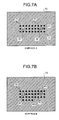
- the internal-layer ground conductor 70 is shown in a simplified form in FIG. 6, the internal-layer ground conductor 70 is basically provided between all layers as a beta ground layer as shown in FIG. 7A to FIG. 7D and FIG. 8.
- FIG. 7A to FIG. 7D depict the surrounding of two signal vias 65 disposed at the left side in FIG. 6, between two layers.
- FIG. 7A (a surface A) depicts a state between a first layer and a second layer
- FIG. 7B (a surface B) depicts a state between a third layer and a fourth layer
- FIG. 7C (a surface C) depicts a state between the fourth layer and a fifth layer
- FIG. 7D (a surface D) depicts a state between the fifth layer and the carrier 22.
- plural ground vias 75 and internal-layer ground conductors 70 are disposed around the two signal vias 65 through a dielectric material 61.
- FIG. 7C the surface C
- two signal vias 65 and the internal-layer signal lines 60 that connect between the two signal vias 65 are disposed, and plural ground vias 75 and internal-layer ground conductors 70 are disposed around the signal vias 65 and the internal-layer signal lines 60 through the dielectric material 61.
- the resistance film 80 to suppress leakage of a high-frequency component to the outside is adhered to the internal-layer signal lines 60, and a slot line 83 is formed on the internal-layer signal lines 60.
- FIG. 7D the surface D
- the signal vias 65 and the internal-layer signal lines 60 are not disposed, and only the ground via 75 and the internal-layer ground conductor 70 are disposed.
- FIG. 8 depicts an example of a wiring pattern in an optional layer.
- plural ground vias 75 and internal-layer ground conductors 70 are disposed around the signal vias 65 through the dielectric material 61.
- plural ground vias 75 and internal-layer ground conductors 70 are disposed around the internal-layer signal lines 60 connected to the signal vias 65 through the dielectric material 61.
- the resistance film 80 to suppress leakage of a high-frequency component to the outside is also applied to the internal-layer signal lines 60.
- the high-frequency package 2 shown in FIG. 2 to FIG. 8 has the following three characteristic structures (a) to (c).
- the high-frequency package 2 has the characteristic structures (a) to (c), and can suppress a discharge of an unnecessary wave of the high-frequency package 2 to the outside.
- a high-frequency component from the high-frequency semiconductor 43 enters via the dielectric material 56 around the bias and control signal pad 50 and the sidewall 55 of the cavity 40, and is electromagnetically coupled to the signal vias 65 or the internal-layer signal lines 60.
- the high-frequency component tries to leak out of the high-frequency package 2 via the internal-layer signal lines 60, the signal vias 65, and the external terminals 51.
- the high-resistance resistance film 80 is applied and adhered to only the upper surface, only the lower surface, or on both surfaces of the internal-layer signal lines 60. Therefore, even when a high-frequency component is electromagnetically coupled to the signal vias 65 or the internal-layer signal lines 60, based on the skin effect, the high-frequency component flows through the resistance film 80 formed on the surface of the internal-layer signal lines 60. The resistance film 80 absorbs this high-frequency component. Consequently, the high-frequency component that enters the internal-layer signal lines 60 cannot transmit to an end of the resistance film 80.
- a bias DC voltage or a low to intermediate frequency signal for a control signal that needs to be passed through the internal-layer signal lines 60 does not flow through the resistance film 80 on the surface layer of the internal-layer signal lines 60. Therefore, the bias DC voltage or the low to intermediate frequency signal for a control signal can pass through the internal-layer signal lines 60 without a voltage drop.
- the resistance film 80 is formed on the internal-layer signal lines 60, the high-frequency signal is absorbed by the resistance film 80 based on the skin effect, thereby suppressing a discharge level of the high-frequency signal in the high-frequency package as a single unit.
- the resistance film 80 can be formed along the total length of the internal-layer signal lines 60, or can be adhered to a part of the internal-layer signal lines 60 such as a signal input side, a signal output side, or signal input and output sides, as shown in FIG. 8.
- the signal input side means an area of the internal-layer signal lines 60 near the signal vias 65 connected to the bias and control signal pads 50 side.
- the signal output side means an area of the internal-layer signal lines 60 near the signal vias 65 connected to the external terminal 51 side.
- FIG. 9 depicts a simplified internal configuration of the high-frequency package 2 shown in FIG. 3 to FIG. 5.
- the high-frequency package 2 having one of the two cavities 40 shown in FIG. 4 and FIG. 5 is shown.
- FIG. 10 depicts the high-frequency package shown in FIG. 19[r]FIG. 9 cut along a line A-A.
- the cover 25 is dismounted.
- the high-frequency package 2 includes the grounded metal carrier 22, the multilayer dielectric substrate 23, the seal ring 24, the cavity 40, the feed-through 42, the high-frequency semiconductor 43, the wire 44, the microstrip line 45, the bias and control signal pad 50, the external terminals 51, the dielectric material 56 around the bias and control signal pad 50, and the ground 57 formed on the surface of the multilayer dielectric substrate 23.
- the external terminals 51 are provided in the high-frequency package 2, and are electrically connected to the bias and control signal pad 50 via the signal vias 65 and the internal-layer signal lines 60.
- a ground pattern (only a side edge surface-layer ground pattern 57 is shown in FIG. 9) is provided on other than the microstrip line 45, the bias and control signal pad 50, and the dielectric material 56 around them.
- the side edge surface-layer ground pattern 57 is connected to the internal-layer ground conductor 70 (refer to FIG. 6) via the ground vias 81 and 75b.
- the dielectric material of the multilayer dielectric substrate 23 is exposed to the sidewall 55 of the cavity 40, as described above.
- the high-frequency signal used in the high-frequency semiconductor 43 is connected to the microstrip line 45 with the wire 44, for example, and is transmitted to the high-frequency semiconductor 43 within the other cavity 40 with the feed-through 42 or the like.
- the bias and control signal to drive or control the high-frequency semiconductor 43 passes from the external terminal 51 to the bias and control signal pads 50 through the signal vias 65 and the internal-layer signal lines 60.
- the bias and control signal is applied to the high-frequency semiconductor 43 from the bias and control signal pads 50 via the wires 44.
- the ground patterns and the ground vias provided in the high-frequency package 2 suppress the high-frequency signal component discharged from the high-frequency semiconductor 43 or the microstrip line 45 to space from being coupled to the bias and control signal.
- the sidewall ground via string 82 having plural sidewall ground vias 81 arranged in a depth direction K is provided near the sidewall 55 of the cavity 40 in the multilayer dielectric substrate 23.
- a distance between the sidewall ground via string 82 and the ground via string 84 consisting of plural ground vias 75b in a shortest distance from the sidewall ground via string 82 sandwiching the signal via 65 is set to less than a half of the effective wavelength ⁇ g of the high-frequency signal used within the high-frequency package 2.
- a distance t between adjacent ground vias in each of the ground via strings 82 and 84 is also set to less than a half of the effective wavelength ⁇ g.
- FIG. 12 depicts a configuration of a high-frequency package not provided with the sidewall ground via string 82 near the sidewall 55 forming the cavity 40.
- the sidewall 55 operates as a high-frequency magnetic wall. Therefore, a magnetic field distribution having the magnetic wall as a symmetrical axis of a maximum electric field value is generated as shown in FIG. 12.
- a distance from the sidewall 55 to the ground via string 84 is La
- a wavelength component of a half-wave length equal to or less than 2La can pass to the depth direction K, and only a wavelength component of a half-wave length larger than 2La cannot pass to the depth direction K.
- the high-frequency component of the effective wavelength ⁇ g can pass to the depth direction K. Therefore, as shown in FIG. 12, when the sidewall ground via string 82 is not provided near the sidewall 55 and also when a distance from the sidewall 55 to the ground via string 84 is equal to or larger than a quarter of the effective wavelength ⁇ g, a high-frequency component that enters via the sidewall 55 or the dielectric material 56 around the bias and control signal pad 50 is coupled within the cavity side edge 71. The high-frequency component passes to the depth direction K, is coupled to the bias and control signal, and leaks via the signal vias 65, the internal-layer signal lines 60, and the external terminal 51.
- the distance t between adjacent ground vias in each of the ground via strings 82 and 84 is set to less than a half of the effective wavelength ⁇ g.
- the adjacent ground vias 81 and 81 (or 75b and 75b) work as cutoff waveguides respectively, thereby suppressing the high-frequency component from entering from the sidewall 55.
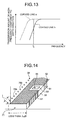
- the distance between the sidewall ground via string 82 and the ground via string 84 is set to less than a half of the effective wavelength ⁇ g. Therefore, a part between the sidewall ground via string 82 and the ground via string 84 works as a cutoff waveguide, and this part has a transmission characteristic like that of a high-pass filter as shown by a curved line b in FIG. 13. Consequently, a transmission amount of a high-frequency component in the frequency area near a frequency f0 or a lower frequency area than the f0 can be decreased.
- FIG. 13 depicts a transmission characteristic of a high-frequency component to the depth direction K at the cavity side edge 71, when a distance between the sidewall ground via string 82 and the ground via string 84 is set to less than a half of the effective wavelength ⁇ g of the high-frequency signal, and when this distance is set to equal to or larger than a half of the effective wavelength ⁇ g, in the configuration shown in FIG. 11, and when the sidewall ground via string 82 is not provided and also when La ⁇ g/4, and when La ⁇ g/4, in FIG. 12, respectively.
- a curved line a expressed by a broken line shows the transmission characteristic when a distance between the sidewall ground via string 82 and the ground via string 84 is set to equal to or larger than a half of the effective wavelength ⁇ g in the configuration shown in FIG. 11, or when the sidewall ground via string 82 is not disposed and also when La ⁇ g/4 as shown in FIG. 12.
- a curved line b expressed by a solid line shows the transmission characteristic when a distance between the sidewall ground via string 82 and the ground via string 84 is set to less than a half of the effective wavelength ⁇ g of the high-frequency signal in the configuration shown in FIG. 11, or when the sidewall ground via string 82 is not disposed and also when La ⁇ g/4 as shown in FIG. 12 (configuration shown in FIG. 22).
- f0 denotes a frequency corresponding to the effective wavelength ⁇ g of the high-frequency signal used within the high-frequency package 2.
- a frequency of a transmission wave transmitted from the radar device 1 is 76 GHz
- f0 76 GHz.
- the sidewall ground via string 82 is not disposed and also when La ⁇ g/4, or when the sidewall ground via string 82 is disposed but the distance between the sidewall ground via string 82 and the ground via string 84 is equal to or larger than a half of the effective wavelength ⁇ g as shown in FIG. 11, a transmission amount of a high-frequency signal to the depth direction K in the frequency f0 corresponding to the effective wavelength ⁇ g of the high-frequency signal is large.
- the transmission characteristic in the depth direction K is like that of the high-pass filter as shown by the curved line b in FIG. 13 as explained above. Consequently, a transmission amount of a high-frequency component in the frequency area near the frequency f0 or a lower frequency area than the f0 can be decreased. Therefore, even when an unnecessary wave enters the multilayer dielectric substrate 23 via the dielectric material 56 around the bias and control signal pad 50 and the sidewall 55 of the cavity 40, the transmission amount in the depth direction at the cavity side edge 71 becomes small.
- FIG. 11 depicts an electric field distribution when the sidewall ground via string 82 is disposed.
- this type of radar device generates a transmission signal by multiplying an oscillation signal. Therefore, when a transmission frequency is 76 GHz, frequency components of 38 GHz, 19 GHz, and the like are present in a mixture. These frequency components can be suppressed from being coupled to the signal vias 65 or the internal-layer signal lines 60.
- the side edge surface-layer ground pattern 57 and the sidewall ground vias 81 are not formed at a part near the sidewall 55 of the exposed part. This is because when the side edge surface-layer ground pattern 57 and the sidewall ground vias 81 are formed at this part, the wire 44 may erroneously contact the ground at the time of wire boding the wire 44 to the bias and control signal pad 50. When this point is not considered, it is of course preferable to cover the whole surrounding of the bias and control signal pad 50 with the side edge surface-layer ground pattern 57 and to provide the sidewall ground vias 81, from the viewpoint of suppressing leakage of a high-frequency component to the outside.
- the microstrip line 45 extending to the depth direction K is provided. Therefore, it is necessary to suppress the passage of the high-frequency component to a direction J perpendicular to the depth direction K, at cavity side edges 71a positioned at both sides of the microstrip line 45. In this case, ground via strings 74 are formed at both sides of the microstrip line 45, thereby suppressing leakage of the high-frequency component to the direction J. Therefore, a length d in the direction K of the cavity side edges 71a does not need to be particularly prescribed by the effective wavelength ⁇ g.
- FIG. 14 depicts a first modification of the high-frequency package shown in FIG. 11.
- plural sidewall ground vias 81 have shapes half cut perpendicularly, and are disposed in contact with the sidewall 55 that constitutes the cavity 40.
- a distance between the sidewall ground via string 82 consisting of plural sidewall ground vias 81 and the ground via string 84 is also set to less than a half of the effective wavelength ⁇ g, and the distance t between the adjacent ground vias in each of the ground via strings 82 and 84 is also set to less than a half of the effective wavelength ⁇ g. Therefore, in the configuration shown in FIG. 14, the entrance of an unnecessary wave to the sidewall 55 of the cavity 40 can be also suppressed, and the passage of the unnecessary wave to the depth direction K can be also suppressed.
- the unnecessary wave can be suppressed from being coupled to the signal via 65 or the internal-layer signal line 60. Consequently, the unnecessary wave can be suppressed from being discharged to outside the high-frequency package 2 via the signal via 65, the internal-layer signal line 60, and the external terminal 51.
- FIG. 15 depicts a second modification of the high-frequency package shown in FIG. 10.
- the whole surface of the sidewall 55 constituting the cavity 40 is metalized with the ground pattern 85.
- a distance between the ground pattern 85 and the ground via string 84 is set to less than a half of the effective wavelength ⁇ g, and the distance t between the adjacent ground vias in the ground via string 84 is set to less than a half of the effective wavelength ⁇ g. Therefore, in the configuration shown in FIG. 15, the entrance of an unnecessary wave to the sidewall 55 of the cavity 40 can be completely suppressed.
- the unnecessary wave enters the multilayer dielectric substrate 23 via the dielectric material 56 around the bias and control signal pad 50, the high-frequency signal can be suppressed from being coupled to the signal via 65 or the internal-layer signal line 60. Consequently, the unnecessary wave can be suppressed from being discharged to outside the high-frequency package 2 via the signal via 65, the internal-layer signal line 60, and the external terminal 51.
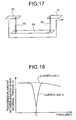
- the slot line 83 having a length of a quarter ⁇ 10% of the effective wavelength ⁇ g is provided in the internal-layer signal line 60 connected to the bias and control signal pad 50.
- a high-frequency component that is coupled to the signal via 65 or the internal-layer signal lines 60 via the sidewall 55 of the cavity 40 or the dielectric material 56 around the bias and control signal pad 50 can be suppressed from transmitting to the internal-layer signal line 60 at the front of the slot line 83. Consequently, leakage of the high-frequency component to the outside via the external terminals 51 can be suppressed.
- FIG. 18 depicts a transmission characteristic of a high-frequency component between the bias and control signal pad 50 and the external terminal 51.
- a curved line c shows the transmission characteristic when the slot line 83 is not provided as shown in FIG. 17, and a curved line d shows the transmission characteristic when the slot line 83 having a length of a quarter ⁇ 10% of the effective wavelength ⁇ g is provided as shown in FIG. 16.
- the curved line c shown in FIG. 18 when the slot line 83 is not provided, the transmission amount of the high-frequency component increases over the total frequency band. Therefore, when a high-frequency component is coupled to the signal via 65 or the internal-layer signal line 60, the high-frequency component leaks outside.
- the function of a band stop filter works, and the transmission amount of the high-frequency component can be decreased extremely in the near band of the frequency f0 corresponding to the effective wavelength ⁇ g of the high-frequency signal. Therefore, a high-frequency component that is coupled to the signal via 65 or the internal-layer signal line 60 can be suppressed from transmitting to the internal-layer signal line 60 at the front of the slot line 83. Consequently, leakage of the high-frequency component to the outside can be suppressed.
- a high-frequency component can be shielded within the high-frequency package 2. Accordingly, leakage of the high-frequency component outside the high-frequency package can be suppressed. Consequently, a high-frequency package, a transmission/reception module, and a radio device having the high-frequency shielding performance can be provided at low cost.
- the present invention is applied to the high-frequency package 2 having the high-frequency semiconductor 43 accommodated within the cavity 40 formed in the multilayer dielectric substrate 23.
- the characteristic structures (a) to (c) can be also applied to the high-frequency package 2 having the high-frequency semiconductor 43 mounted on the surface layer of the multilayer dielectric substrate 23 having no cavity 40.
- FIG. 20 depicts a transmission characteristic of the low-pass filter 86.
- This low-pass filter 86 cuts a frequency component equal to or higher than a predetermined frequency f1 lower than the frequency f0 corresponding to the effective wavelength ⁇ g of the high-frequency signal.
- the low-pass filter 86 is effective when many wavelength components near the effective wavelength ⁇ g are present.
- the low-pass filter 86 is provided in the internal-layer signal line 60. Consequently, the high-frequency component coupled to the signal via 65 or the internal-layer signal line 60 can be suppressed from transmitting to the internal-layer signal line 60 in front of the low-pass filter 86. As a result, leakage of a high-frequency component to the outside can be suppressed.
- FIG. 21 depicts a high-frequency package 2' according to the third embodiment.
- like reference numerals denote like constituent elements that achieve the same functions as the constituent elements of the high-frequency package 2 shown in FIG. 6, and a redundant explanation is omitted.
- the high-frequency package 2' shown in FIG. 21 is double-side mounted.
- a high-frequency semiconductor (or an electronic circuit part concerning the high-frequency semiconductor) 66 is also mounted on a rear surface of the multilayer dielectric substrate 23.
- the high-frequency semiconductor 66 is shielded by the carrier 22 and a back-surface cover 67.
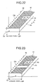
- the sidewall ground vias 81 shown in FIG. 11 or the ground pattern 85 shown in FIG. 15 is not provided near the sidewall 55 that constitutes the cavity 40.
- the sidewall 55 is in a non-grounded state, with the dielectric material exposed.
- a distance between the sidewall 55 and the ground via string 84 consisting of plural ground vias 75b in a shortest distance from the sidewall 55 sandwiching the signal via 65 is set to less than a quarter of the effective wavelength ⁇ g of the high-frequency signal used within the high-frequency package 2.
- the sidewall 55 works as a magnetic wall like that shown in FIG. 12, and has an electric field distribution similar to that shown in FIG. 12.
- a distance Lb between the sidewall 55 and the ground via string 84 is set to less than a quarter of the effective wavelength ⁇ g. Therefore, a high-frequency component of the effective wavelength ⁇ g cannot pass to the depth direction K. In other words, a high-frequency signal of the effective wavelength ⁇ g is cut off in the depth direction K, as shown in FIG. 13.
- the resistance film 80 which absorbs the high-frequency signal based on the skin effect, is formed on the internal-layer signal lines 60, thereby suppressing a discharge level of the high-frequency signal in the high-frequency package as a single unit.
- the high-frequency signal can be suppressed from transmitting to the depth direction K. Therefore, the high-frequency signal can be suppressed from being coupled to the signal vias 65 or the internal-layer signal lines 60. As a result, an unnecessary wave can be suppressed from being discharged to outside the high-frequency package 2 through the signal vias 65, the internal-layer signal lines 60, and the external terminals 51. Since the resistance film 80 is formed on the internal-layer signal lines 60, the high-frequency signal can be suppressed from being discharged to outside the high-frequency package 2 through the external terminals 51.
- a fourth embodiment of the present invention is explained below with reference to FIG. 23.
- the fourth embodiment is a modification of the third embodiment.
- the difference between the fourth embodiment and the third embodiment lies in that a part of the side edge surface-layer ground pattern 57 formed on the upper surface of the cavity side edge 71 of the multilayer dielectric substrate 23 is extracted, and a dielectric material is exposed at a ground-extracted part 87.
- the distance Lb between the sidewall 55, on which the dielectric material is exposed, and the ground via string 84 is set to less than a quarter of the effective wavelength ⁇ g.
- a high-frequency component that is coupled inside the cavity side edge 71 can be discharged to the internal space encircled by the seal ring 24 and the cover 25 via the ground-extracted part 87.
- the high-frequency component that enters the inside of the cavity side edge 71 is extracted to the above via the ground-extracted part 87.
- a high-frequency component that is coupled inside the cavity side edge 71 can be discharged to the internal space. Therefore, a coupling of the high-frequency component to the bias or control signal can be further decreased. Consequently, an unnecessary wave can be suppressed from being discharged outside the high-frequency package.
- the ground-extracted part 87 can be also provided in the cavity side edge 71 of the high-frequency package 2 according to the first embodiment.
- a fifth embodiment of the present invention is explained below with reference to FIG. 24 and Figs. 25A to 25D.
- the characteristic structure (b) explained in the first embodiment is applied to a high-frequency package 91 mounted with a flip-chip high-frequency semiconductor (MMIC) 90.
- MMIC flip-chip high-frequency semiconductor
- the flip-chip high-frequency semiconductor 90 shown in FIG. 24 has many bumps 92 on its bottom surface.
- the high-frequency semiconductor 90 is connected to the multilayer dielectric substrate 23 via these bumps 92.
- FIG. 25A depicts the back surface of the high-frequency semiconductor 90, that is, a layout example of the bumps 92.
- ground bumps 92b expressed in black color are disposed around signal bumps 92a expressed in outline.
- the multilayer dielectric substrate 23 is formed on the grounded carrier 22.
- the seal ring 24 and the cover 25 are formed on the multilayer dielectric substrate 23.
- the high-frequency semiconductor 90 is shielded with the seal ring 24 and the cover 25.
- the high-frequency semiconductor 90 is mounted by flip-chip bonding on a conductor pad 94 provided on the upper layer of the multilayer dielectric substrate 23.
- a surface-layer ground conductor 93, the internal-layer ground conductor 70, and the internal-layer signal line 60 are suitably formed on each layer of the multilayer dielectric substrate 23, in a similar manner to that of the high-frequency package 2 shown in FIG. 6 according to the first embodiment.
- the internal-layer ground conductor 70, the surface-layer ground conductor 93, and the carrier 22 are connected to each other with the ground vias 75.
- the signal bumps 92a and the external terminal 51 are connected to each other with the signal vias 65 and the internal-layer signal lines 60.
- FIG. 25D [r] 25B (the surface A) depicts a part of a via structure on the first-layer surface layer immediately below the high-frequency semiconductor 90.
- the signal vias 65 and the ground vias 75 are disposed corresponding to the layout of the signal bumps 92a and the ground bumps 92b.
- FIG. 25C (the surface B) depicts a part of a via structure on the second-layer surface layer immediately below the high-frequency semiconductor 90.
- FIG. 25D (the surface C) depicts a part of a via structure on the third-layer surface layer immediately below the high-frequency semiconductor 90.
- the internal-layer signal line 60 is formed on the third-layer surface layer shown as the surface C.
- distances D1 and D2 between the ground vias 75 (the ground via string) that sandwich the signal vias 65 are set to less than a half of the effective wavelength ⁇ g of the high-frequency semiconductor 90 mounted on the high-frequency package 91, as shown in FIG. 24 and FIG. 25B.
- the coupling of the high-frequency component to the signal vias 65 and the internal-layer signal lines 60 can be suppressed. Consequently, a high-frequency component can be suppressed from being discharged to outside the high-frequency package 2 via the signal vias 65, the internal-layer signal lines 60, and the external terminal 51.
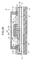
- a sixth embodiment of the present invention is explained below with reference to FIG. 26.
- the characteristic structure (a) explained in the first embodiment is applied to the high-frequency package 91 provided with the flip-chip high-frequency semiconductor (MMIC) 90.
- MMIC flip-chip high-frequency semiconductor
- the flip-chip high-frequency semiconductor 90 shown in FIG. 26 has many bumps 92 on its bottom surface.
- the high-frequency semiconductor 90 is connected to the multilayer dielectric substrate 23 via these bumps 92.
- a reference numeral 92a denotes a signal bump
- 92b denotes a ground bump.
- the multilayer dielectric substrate 23 is formed on the grounded carrier 22.
- the seal ring 24 and the cover 25 are formed on the multilayer dielectric substrate 23.
- the high-frequency semiconductor 90 is shielded with the seal ring 24 and the cover 25.
- the high-frequency semiconductor 90 is mounted by the flip-chip bonding on a conductor pad 94 provided on the upper surface of the multilayer dielectric substrate 23.
- the surface-layer ground conductor 93, the internal-layer ground conductor 70, and the internal-layer signal line 60 are suitably formed on each layer of the multilayer dielectric substrate 23, in a similar manner to that of the high-frequency package 2 shown in FIG. 6 according to the first embodiment.
- the internal-layer ground conductor 70, the surface-layer ground conductor 93, and the carrier 22 are connected to each other with the ground vias 75.
- the signal bumps 92a and the external terminal 51 are connected to each other with the signal vias 65 and the internal-layer signal lines 60.
- a resistance film 80a is formed at the signal input side of the internal-layer signal line 60, and a resistance film 80b is formed at the signal output side of the internal-layer signal line 60.
- the resistance films 80a and 80b absorb the high-frequency signal based on the skin effect. Consequently, a high-frequency signal can be suppressed from being discharged to outside the high-frequency package 2 via the signal vias 65, the internal-layer signal lines 60, and the external terminal 51.
- the characteristic structure (c) can be also applied to the flip-chip high-frequency package.
- the high-frequency package, the transmission/reception module, and the radar device according to the present invention can be used for a radio device that uses electromagnetic waves of a milliwave band and a microwave band at low cost.
Landscapes
- Engineering & Computer Science (AREA)
- Microelectronics & Electronic Packaging (AREA)
- Production Of Multi-Layered Print Wiring Board (AREA)
Abstract
Description
- The present invention relates to a high-frequency package that includes a high-frequency semiconductor that operates in a high-frequency band such as a microwave band and a milliwave band, a transmission/reception module, and a radio device that include the high-frequency package. More particularly, the present invention relates to a high-frequency package that can suppress leakage of a high-frequency signal generated from the high-frequency semiconductor to outside, a transmission/reception module; and a radio device that include the high-frequency package.
- Conventionally, radio device, for example, a milliwave radar mounted on a vehicle uses electromagnetic waves of a milliwave band, and detects a distance and a relative speed between the vehicle and a vehicle running in front to be applied to achieve a cruise control and a safety measure to reduce damage on a driver when a collision cannot be avoided. In many cases, such an in-vehicle milliwave radar multiplies 1/N (where N is a positive integer of 2 or larger) of a frequency to obtain a high-frequency transmission signal of a milliwave band. In this case, many frequency components are present in a module. Therefore, it is very difficult to satisfy a desired electromagnetic interference (EMI) characteristic.
- In the in-vehicle milliwave radar, a transmission/reception module usually includes a high-frequency package including a high-frequency semiconductor for a radar device, a control/interface substrate that applies a bias signal and a control signal to the high-frequency package, and a waveguide. To satisfy the EMI characteristic, conventionally, a whole body of the transmission/reception module is configured to be covered with a metallic cover.
- However, when such a configuration that the transmission/reception module is covered with the metallic cover is applied, an expensive casing and the like are necessary. Therefore, to reduce manufacturing cost, it is necessary to take measures within the high-frequency package.
- According to
patent literature 1, an integrated circuit part for a high-frequency signal and a dielectric substrate are mounted on a metallic base member, with a micro slip line formed on the dielectric substrate. These parts are covered with a metallic frame member and a metallic lid member. To the integrated circuit part for a high-frequency signal mounted on the base, a bias is applied via a bias terminal. - Patent Literature 1:
Japanese Patent Application Laid-Open No. 2000-31812 - In the above conventional technique, a high-frequency package is covered with a metallic base, a metallic frame member, and a metallic lid member. Therefore, leakage of a high-frequency component to the outside is suppressed to some extent, however, no countermeasure is taken against leakage of a high-frequency component via the bias terminal. Consequently, there is a problem that an unnecessary high-frequency component that is electromagnetically coupled to the dielectric substrate in the high-frequency package and the bias terminal is discharged straight to the outside via the bias terminal.
- In view of the above problems, it is an object of the present invention to provide a high-frequency package, a transmission/reception module, and a radio device having high-frequency shielding performance at low cost, by providing a structure, inside the high-frequency package, to suppress leakage of a high-frequency component outside.
- To solve the above problems and achieve the object, according to the present invention, a high-frequency package includes a high-frequency semiconductor; a multilayer dielectric substrate having the high-frequency semiconductor mounted on a surface-layer ground conductor; and an electromagnetic shielding member configured to cover a part of a surface layer of the multilayer dielectric substrate and the high-frequency semiconductor. The multilayer dielectric substrate includes a first signal via configured to be connected to a bias-and-control-signal terminal of the high-frequency semiconductor, and arranged inside the electromagnetic shielding member; a second signal via arranged outside the electromagnetic shielding member, and configured to be connected to an external terminal for a bias and control signal; an internal-layer signal line configured to connect between the first signal via and the second signal via; an internal-layer ground conductor arranged around the first signal via, the second signal via, and the internal-layer signal line; and a plurality of ground vias arranged around the first signal via, the second signal via, and the internal-layer signal line, on the internal-layer ground conductor. A resistance film is provided on at least one of an upper surface and a lower surface of the internal-layer signal line.
- According to the present invention, the resistance film is provided on at least one of the upper surface and the lower surface of the internal-layer signal line through which the bias and control signal is transmitted. Therefore, a resistive element absorbs the high-frequency signal coupled to the internal-layer signal line, based on the skin effect, and a bias voltage or a control signal can be transmitted without a voltage drop.
- According to a next aspect of the present invention, a high-frequency package includes a high-frequency semiconductor including a bias-and-control-signal terminal; a multilayer dielectric substrate including a surface-layer ground conductor configured to mount the high-frequency semiconductor; and an electromagnetic shielding member configured to cover a part of a surface layer of the multilayer dielectric substrate and the high-frequency semiconductor. The multilayer dielectric substrate includes a first signal via configured to be connected to the bias-and-control-signal terminal, and arranged inside the electromagnetic shielding member; a second signal via arranged outside the electromagnetic shielding member, and configured to be connected to an external terminal for a bias and control signal; an internal-layer signal line configured to connect between the first signal via and the second signal via; an internal-layer ground conductor arranged around the first signal via, the second signal via, and the internal-layer signal line; and a plurality of ground vias arranged around the first signal via, the second signal via, and the internal-layer signal line, on the internal-layer ground conductor. A slot line having a length approximately a quarter of an effective wavelength of a high-frequency signal used in the high-frequency semiconductor is provided on the internal-layer signal line.
- According to the present invention, a slot line having a length of approximately a quarter of an effective wavelength of a high-frequency signal used in a high-frequency semiconductor is provided on an internal-layer signal line for a bias and control signal. With this arrangement, even when a high-frequency component enters a multilayer dielectric substrate from a dielectric layer on a surface layer of the multilayer dielectric substrate and is electromagnetically coupled to a signal via for the bias and control signal or to an internal-layer signal line, the high-frequency component is reflected at the position of the slot line, thereby suppressing passage of the high-frequency component to an external terminal.
- According to a next invention, a high-frequency package includes a high-frequency semiconductor; a multilayer dielectric substrate including a surface-layer ground conductor configured to mount the high-frequency semiconductor, and an internal-layer ground conductor configured to be connected to the surface-layer ground conductor; and an electromagnetic shielding member configured to cover a part of a surface layer of the multilayer dielectric substrate and the high-frequency semiconductor. The multilayer dielectric substrate includes a first signal via configured to be connected to a bias-and-control-signal terminal of the high-frequency semiconductor, and arranged inside the electromagnetic shielding member; a second signal via arranged outside the electromagnetic shielding member, and configured to be connected to an external terminal for a bias and control signal; an internal-layer signal line configured to connect between the first signal via and the second signal via; a first ground via string arranged at a portion closer to the high-frequency semiconductor than the first signal via, and including a plurality of ground vias configured to be connected to the internal-layer ground conductor; and a second ground via string arranged between the first signal via and the second signal via, and including a plurality of ground vias configured to be connected to the internal-layer ground conductor. A distance between the first ground via string and the second ground via string is less than a half of an effective wavelength of a high-frequency signal used in the high-frequency semiconductor, and a distance between adjacent ground vias in the first and the second ground via strings respectively is less than a half of the effective wavelength of the high-frequency signal used in the high-frequency semiconductor.
- According to the invention, a distance between a first ground via string and a second ground via string is set to less than a half of an effective wavelength of a high-frequency signal used in a high-frequency semiconductor. With this arrangement, entrance of a high-frequency component to a direction along the ground via within the multilayer dielectric substrate can be suppressed. Since the distance between the first ground via string and the second ground via string is set to less than a half of the effective wavelength of a high-frequency signal used in the high-frequency semiconductor, entrance of a high-frequency component to a direction perpendicular to the ground via string within the multilayer dielectric substrate is also suppressed.
- According to the present invention, a resistance film is provided on at least one of the upper surface and the lower surface of the internal-layer signal line through which the bias and control signal is transmitted. Therefore, a resistive element absorbs the high-frequency signal coupled to the internal-layer signal line, based on the skin effect, and a bias voltage or a control signal can be transmitted without a voltage drop. Accordingly, based on a low-cost configuration, the high-frequency signal can be suppressed from being discharged to the outside of the high-frequency package through the signal via, the internal-layer signal line, and the external terminal.
- According to the next invention, a slot line having a length of approximately a quarter of an effective wavelength of a high-frequency signal used in a high-frequency semiconductor is provided on an internal-layer signal line for a bias and control signal. With this arrangement, a high-frequency component that enters a multilayer dielectric substrate is reflected at the position of the slot line, thereby suppressing passage of the high-frequency component to an external terminal. Therefore, leakage of a high-frequency component to the outside of the high-frequency package can be securely suppressed. Since the leakage of the high-frequency component to the outside of the high-frequency package can be suppressed inside the high-frequency package, manufacturing cost can be decreased.
- According to the next invention, a distance between a first ground via string and a second ground via string is set to less than a half of an effective wavelength of a high-frequency signal used in a high-frequency semiconductor. With this arrangement, entrance of a high-frequency component to a direction along the ground via within the multilayer dielectric substrate can be suppressed. Since the distance between the first ground via string and the second ground via string is set to less than a half of the effective wavelength of a high-frequency signal used in the high-frequency semiconductor, entrance of a high-frequency component to a direction perpendicular to the ground via string within the multilayer dielectric substrate is also suppressed. Therefore, according to the present invention, a coupling of a high-frequency signal to the signal via within the multilayer dielectric substrate or to the internal-layer signal line can be suppressed. Further, discharging of an unnecessary wave to the outside of the high-frequency package via the signal via, the internal-layer signal line, and the external terminal can be suppressed.
-
- FIG. 1 is a functional block diagram of an FM-CW radar device to which the present invention is applied;
- FIG. 2 is a cross-section of a configuration of a transmission/reception module;
- FIG. 3 is a perspective view of a high-frequency package according to a first embodiment of the present invention;
- FIG. 4 is a perspective view of the high-frequency package according to the first embodiment when a cover is dismounted;
- FIG. 5 is a plan view of the high-frequency package according to the first embodiment;
- FIG. 6 is a detailed cross-section of a via structure of a multilayer dielectric substrate of the high-frequency package;
- FIG. 7A is a schematic for illustrating a surface A of the multilayer dielectric substrate shown in FIG. 6;
- FIG. 7B is a schematic for illustrating a surface B of the multilayer dielectric substrate shown in FIG. 6;
- FIG. 7C is a schematic for illustrating a surface C of the multilayer dielectric substrate shown in FIG. 6;
- FIG. 7D is a schematic for illustrating a surface D of the multilayer dielectric substrate shown in FIG. 6;
- FIG. 8 is a plan view of a layout pattern of an internal-layer signal line, an internal-layer ground conductor, a ground via, and a signal via;
- FIG. 9 is a perspective view of a simplified internal configuration of the high-frequency package;
- FIG. 10 is a partially enlarged view of FIG. 9;
- FIG. 11 is a partially enlarged view of FIG. 10;
- FIG. 12 is a schematic for illustrating a high-frequency package according to a conventional technique;
- FIG. 13 is a characteristic plot of a high-frequency component to a depth direction;
- FIG. 14 is a perspective view of a modification of the high-frequency package according to the first embodiment;
- FIG. 15 is a perspective view of another modification of the high-frequency package according to the first embodiment;
- FIG. 16 is a partially enlarged view of FIG. 10;
- FIG. 17 is a schematic of the high-frequency package according to the conventional technique;
- FIG. 18 is a characteristic plot of transmission of a high-frequency component between a bias pad and an external terminal;
- FIG. 19 is a partially enlarged view of a high-frequency package according to a second embodiment of the present invention;
- FIG. 20 is a characteristic plot of transmission an LPF according to the second embodiment;
- FIG. 21 is a cross-section of a high-frequency package according to a third embodiment of the present invention;
- FIG. 22 is a partially enlarged view of the high-frequency package according to the third embodiment;
- FIG. 23 is a partially enlarged view of a high-frequency package according to a fourth embodiment of the present invention;
- FIG. 24 is a cross-section of a high-frequency package according to a fifth embodiment of the present invention;
- FIG. 25A is a schematic of a rear surface of a high-frequency semiconductor that is mounted on the high-frequency package according to the fifth embodiment;
- FIG. 25B is a schematic of a surface A of a multilayer dielectric substrate shown in FIG. 24;
- FIG. 25C is a schematic of a surface B of the multilayer dielectric substrate shown in FIG. 24;
- FIG. 25D is a schematic of a surface C of the multilayer dielectric substrate shown in FIG. 24; and
- FIG. 26 is a cross-section of a high-frequency package according to a sixth embodiment of the present invention.
-
- 1
- Radar device
- 2, 2', 91
- High-frequency packages
- 3
- Control circuit
- 4
- Modulation circuit
- 6
- Transmission/reception module
- 7
- Antenna
- 8
- Signal processing substrate
- 10
- Casing
- 12
- Radome
- 13
- Cable
- 14
- Connector
- 16
- Waveguide
- 17
- Waveguide plate
- 19
- Electronic circuit
- 21
- Module control substrate
- 22
- Carrier
- 23
- Multilayer dielectric substrate
- 24
- Seal ring
- 25
- Cover
- 30
- Oscillator
- 32
- Power distributor
- 33
- Multiplier
- 35
- Transmission waveguide terminal
- 36
- Reception waveguide terminal
- 37
- MMIC
- 39
- Mixer
- 40
- Cavity
- 42
- Feed-through
- 43, 66, 90
- High-frequency semiconductors
- 41, 44
- Wires
- 45
- Microstrip line
- 50
- Bias and control signal pad
- 51, 52
- External terminals
- 53
- Ground surface
- 55
- Sidewall
- 56, 61
- Dielectric material
- 57
- Side edge surface-layer ground pattern
- 60
- Internal-layer signal line
- 65
- Signal via
- 70
- Internal-layer ground conductor
- 71, 71a
- Cavity side edges
- 75, 75a, 75b, 75c
- Ground vias
- 80
- Resistance film
- 81
- Sidewall ground via
- 82
- Sidewall ground via string
- 83
- Slot line
- 84
- Ground via string (shield via string)
- 85
- Ground pattern
- 86
- Low-pass filter
- 87
- Ground-extracted part
- 92
- Bump
- 92a
- Signal bump
- 92b
- Ground bump
- 93
- Surface-layer ground conductor
- 94
- Conductor pad
- λg
- Effective wavelength
- Exemplary embodiments of a high-frequency package, a transmission/reception module, and a radar device according to the present invention will be explained in detail with reference to the accompanying drawings. The present invention is not limited by the embodiments.
- A first embodiment of the present invention is explained below with reference to FIG. 1 to FIG. 18. FIG. 1 is a functional block diagram of a
radar device 1 that includes a radio device to which the present invention is applied. A functional internal configuration of theradar device 1 is explained first with reference to FIG. 1. - The
radar device 1 is an FM-CW radar having a function of detecting a distance and a relative speed between with respect to a target object (such as a vehicle) in front, using electromagnetic waves of a milliwave band (for example, 76 GHz). The FM-CW radar irradiates a frequency modulated high-frequency signal (a transmission signal) to the target, detects a difference in frequency between the transmission signal and a signal reflected from the target (a reception signal), and calculates a distance and a relative speed with respect to the target. - As shown in FIG. 1, the
radar device 1 includes a transmission/reception module 6, anantenna 7 that is formed with a transmission/reception antenna, and asignal processing substrate 8 that is connected to an external device to carry out various kinds of signal processing. The transmission/reception module 6 includes a high-frequency package 2, acontrol circuit 3 that drive controls various kinds of high-frequency semiconductor elements within the high-frequency package 2, and amodulation circuit 4. - The
signal processing substrate 8 has a function of controlling theentire radar device 1, and analyzes a frequency of a fast Fourier transform (FFT) based on a video signal obtained from the transmission/reception module 6, thereby acquiring a distance and a relative speed with respect to the target. - The
modulation circuit 4 outputs a transmission-frequency modulating voltage in accordance with a control signal from thesignal processing substrate 8. Thecontrol circuit 3 operates based on an input control signal (such as a synchronous clock), and outputs a bias voltage, a control signal of a monolithic microwave IC (MMIC), and a modulation signal to thepackage 2. - The high-
frequency package 2 includes a voltage control oscillator (VCO) 30, apower distributor 32, amultiplier 33, anamplifier 34, atransmission terminal 35 formed with a waveguide terminal, areception terminal 36, a low-noise amplifier (LNA) 38, and a mixer (MIX) 39. The high-frequency package 2 has a size of, for example, 10 mm to 40 mm square. - Operation of the respective units is explained next. The
voltage control oscillator 30 outputs a frequency modulated high-frequency signal. Thepower distributor 32 distributes the output from thevoltage control oscillator 30 to two directions. Themultiplier 33 receives one of the outputs from thepower distributor 32, multiplies the frequency by N (where N is a positive integer and N≥2), and outputs the multiplied result. Theamplifier 34 power amplifies the output from themultiplier 33, and outputs a transmission signal to thetransmission terminal 35. This transmission signal is transmitted to theantenna 7 via a waveguide, and is discharged to space. - The
antenna 7 receives a reception wave reflected from the target. The reception wave that is output from theantenna 7 is input to theamplifier 38 via thereception terminal 36. Theamplifier 38 performs low-noise amplification on the output from theantenna 7. Themixer 39 outputs a video signal having a sum of and a difference between the N-time frequency of the signal of the high-frequency signal input from thepower distributor 32 and the output frequency of theamplifier 38, to thesignal processing substrate 8. Thesignal processing substrate 8 analyzes the frequency of a fast Fourier transform (FFT) based on the video signal, and calculates a distance and a relative speed with respect to the target. The calculated distance and relative speed with respect to the target are transmitted to the external device. - The
radar device 1 includes the transmission/reception module 6, thesignal processing substrate 8, and acable 13 including a power supply line and an input/output signal line to thesignal processing substrate 8. - FIG. 2 is a cross-section of the transmission/
reception module 6. As shown in FIG. 2, the transmission/reception module 6 has awaveguide plate 17 formed with awaveguide 16 that is connected to thetransmission terminal 35 and thereception terminal 36 shown in FIG. 1. Theantenna 7 is connected to the lower surface of thewaveguide plate 17. The transmission/reception module 6 also includes the high-frequency package 2 mounted on the upper surface of thewaveguide plate 17, and a module control substrate (also called a control/interface substrate) 21 on which anelectronic circuit 19 constituting thecontrol circuit 3 or themodulation circuit 4 shown in FIG. 1 is mounted. In FIG. 2, a groundedmetal carrier 22, amultilayer dielectric substrate 23, aseal ring 24, and acover 25 are shown as elements that constitute the high-frequency package 2. - FIG. 3 is a perspective view of the high-
frequency package 2, and FIG. 4 is a perspective view of the high-frequency package 2 with a cover dismounted. As shown in FIG. 3 and FIG. 4, a side surface of themultilayer dielectric substrate 23 has a staged shape, andexternal terminals 51 are formed on an upper surface of the stage. As shown in FIG. 4, a surface X1 on which thecover 25 is fit is formed on an upper surface of themultilayer dielectric substrate 23. Cavities X2 and X3 facing above are formed on an upper surface of themultilayer dielectric substrate 23. A smallerconcave cavity 40 is provided within the cavities X2 and X3 respectively. AnMMIC 37 is accommodated and mounted within thecavity 40. - FIG. 5 is a plan view of the high-
frequency package 2 with thecover 25 dismounted. As shown in FIG. 2 and FIG. 5, the groundedmetal carrier 22, and themodule control substrate 21 mounted with theelectronic circuit 19 constituting thecontrol circuit 3 and themodulation circuit 4 are mounted on thewaveguide plate 17 formed with thewaveguide 16. Awaveguide 27 is also formed in thecarrier 22. Thecarrier 22 is fixed to thewaveguide plate 17 by inserting ascrew 26 into ascrew hole 26a formed in aflange 28. Themultilayer dielectric substrate 23 is mounted on thecarrier 22. One or plural (two, in the present example) concaves, that is, thecavities 40, are formed at a center of themultilayer dielectric substrate 23. - Plural high-frequency semiconductors, that is,
MMICs 43 included in the high-frequency package 2 shown in FIG. 1 are accommodated on a bottom surface (the upper surface) [d]41 of thecavity 40. The high-frequency semiconductor 43 herein is a generic name of the voltage control oscillator (VCO) 30, thepower distributor 32, themultiplier 33, theamplifier 34, the low-noise amplifier (LNA) 38, and the mixer (MIX) 39 included in the high-frequency package 2 shown in FIG. 1. - As shown in FIG. 5, a reception system high-frequency semiconductor such as the low-noise amplifier (LNA) 38 and the mixer (MIX) 39 is accommodated in one of the cavities (the upper side in FIG. 5) 40, and a transmission system high-frequency semiconductor such as the voltage control oscillator (VCO) 30, the
power distributor 32, themultiplier 33, and theamplifier 34 is accommodated in the other (the lower side in FIG. 5)cavity 40. - The frame-shaped
seal ring 24 made of metal that shields an unnecessary discharging from the high-frequency semiconductor 43 to outside is mounted on themultilayer dielectric substrate 23. Thecover 25 is provided on theseal ring 24. Theseal ring 24 and thecover 25 constitute an electromagnetic shielding member that covers a part of the surface layer of themultilayer dielectric substrate 23 and the high-frequency semiconductor 43. - As shown in FIG. 5, a feed-through 42 is provided in a seal ring 24' that partitions the two
cavities 40. The mixer (MIX) 39 accommodated in theupper cavity 40 and thepower distributor 32 accommodated in thelower cavity 40 are connected by the feed-through 42 and amicrostrip line 45. The feed-through 42 covers a signal pin or a microstrip line with a dielectric material. With this arrangement, a high-frequency signal is transmitted between the twocavities 40 while holding eachcavity 40 in an airtight state. In FIG. 5, areference numeral 56 denotes a microstrip-waveguide converter. - A conductor pad (hereinafter, "bias and control signal pad") 50 that supplies a bias voltage to the high-
frequency semiconductor 43 or inputs and outputs a control signal to and from the high-frequency semiconductor 43 is provided on themultilayer dielectric substrate 23. A conductor pad (a bias and control signal terminal) 49 is also provided on the high-frequency semiconductor 43. The bias andcontrol signal pad 50 is connected to theconductor pad 49 of the high-frequency semiconductor 43, and the high-frequency semiconductor 43 is connected to themicrostrip line 45, respectively by wire bonding using awire 44 made of metal or the like. Alternatively, these units can be connected to each other with a metal bump or a ribbon, in place of thewire 44. - The
external terminals 51 are provided on themultilayer dielectric substrate 23 at the outside of theseal ring 24. As shown in FIG. 6, theexternal terminals 51 are electrically connected to the bias andcontrol signal pad 50 provided on themultilayer dielectric substrate 23 inside theseal ring 24 via a signal via 65 (a signal through hole) formed in themultilayer dielectric substrate 23 and internal-layer signal lines 60. As shown in FIG. 2, theseexternal terminals 51 are connected to anexternal terminal 52 formed on themodule control substrate 21 via thewire 41. As shown in FIG. 2, aresistance film 80 is adhered to the internal-layer signal lines 60. Theresistance film 80 suppresses leakage of a high-frequency component (unnecessary wave) to the outside via the internal-layer signal lines 60. Theresistance film 80 is described in detail later. - FIG. 6 depicts, in detail, the via structure (through hole structure) inside the
multilayer dielectric substrate 23 of the high-frequency package 2. In FIG. 6, the bias control signal via (hereinafter, "signal via") 65 is expressed in an outline, and a ground via 75 is expressed in a hatched line. In this example, thecavity 40 is formed on themultilayer dielectric substrate 23 by removing a center part of a first layer of themultilayer dielectric substrate 23. Aground surface 53 is formed as a surface-layer ground conductor on a bottom surface of thecavity 40, that is, on the surface of a third layer. The high-frequency semiconductor 43 is mounted on theground surface 53 via a solder or aconductive adhesive 54.Plural ground vias 75a that connect between theground surface 53 and thecarrier 22 are provided on theground surface 53 disposed beneath the high-frequency semiconductor 43. - In this case, the dielectric material is exposed on a sidewall 55 (a sidewall surface of the first layer of the multilayer dielectric substrate 23) of the
cavity 40. One or plural bias andcontrol signal pads 50 are provided on the surface layer (the upper surface layer) of the first layer of themultilayer dielectric substrate 23. Parts other than apart 56 at which the dielectric material is exposed around the bias andcontrol signal pad 50 are formed with aground pattern 57 as a surface-layer ground conductor, thereby preventing a high-frequency signal from entering inside themultilayer dielectric substrate 23 through the surface layer. - An RF shielding via 75b to shield a high-frequency component generated from the high-
frequency semiconductor 43 is provided near a portion right under theseal ring 24 in the first layer of themultilayer dielectric substrate 23. PluralRF shielding vias 75b are also arranged in a direction perpendicular to the paper surface. An area from thesidewall 55 of thecavity 40 to where the RF shielding via 75b is provided in the first layer of themultilayer dielectric substrate 23 is called acavity side edge 71. Theground pattern 57 provided on the surface layer of thecavity side edge 71 is called a side edge surface-layer ground pattern. The RF shielding via 75b is connected to the side edge surface-layer ground pattern 57 and an internal-layer ground conductor 70 that is formed on the internal layer of themultilayer dielectric substrate 23. - The bias and
control signal pads 50 disposed inside theseal ring 24 are connected to theexternal terminals 51 disposed at the outside of theseal ring 24 via one orplural signal vias 65 and one or plural internal-layer signal lines 60.Plural ground vias 75c are disposed to sandwich a dielectric material around the signal via 65. Theseground vias 75c shield electric fields from thesignal vias 75. - While the internal-
layer ground conductor 70 is shown in a simplified form in FIG. 6, the internal-layer ground conductor 70 is basically provided between all layers as a beta ground layer as shown in FIG. 7A to FIG. 7D and FIG. 8. - FIG. 7A to FIG. 7D depict the surrounding of two
signal vias 65 disposed at the left side in FIG. 6, between two layers. FIG. 7A (a surface A) depicts a state between a first layer and a second layer, FIG. 7B (a surface B) depicts a state between a third layer and a fourth layer, FIG. 7C (a surface C) depicts a state between the fourth layer and a fifth layer, and FIG. 7D (a surface D) depicts a state between the fifth layer and thecarrier 22. - On surfaces shown in FIG. 7A (the surface A) and FIG. 7B (the surface B), plural ground vias 75 and internal-
layer ground conductors 70 are disposed around the twosignal vias 65 through adielectric material 61. On a surface in FIG. 7C (the surface C), twosignal vias 65 and the internal-layer signal lines 60 that connect between the twosignal vias 65 are disposed, and plural ground vias 75 and internal-layer ground conductors 70 are disposed around thesignal vias 65 and the internal-layer signal lines 60 through thedielectric material 61. Theresistance film 80 to suppress leakage of a high-frequency component to the outside is adhered to the internal-layer signal lines 60, and aslot line 83 is formed on the internal-layer signal lines 60. On a surface shown in FIG. 7D (the surface D), thesignal vias 65 and the internal-layer signal lines 60 are not disposed, and only the ground via 75 and the internal-layer ground conductor 70 are disposed. - FIG. 8 depicts an example of a wiring pattern in an optional layer. As shown in FIG. 8, plural ground vias 75 and internal-
layer ground conductors 70 are disposed around the signal vias 65 through thedielectric material 61. At a position where the internal-layer signal lines 60 are present, plural ground vias 75 and internal-layer ground conductors 70 are disposed around the internal-layer signal lines 60 connected to the signal vias 65 through thedielectric material 61. In the example shown in FIG. 8, theresistance film 80 to suppress leakage of a high-frequency component to the outside is also applied to the internal-layer signal lines 60. - The high-
frequency package 2 shown in FIG. 2 to FIG. 8 has the following three characteristic structures (a) to (c). -
- (a) As shown in FIG. 2 and FIGs. 6 to 8, the
resistance film 80 is provided on at least one of the upper surface and the lower surface of the internal-layer signal lines 60. With this arrangement, the resistive element absorbs, based on the skin effect, a high-frequency signal that enters via thesidewall 55 of thecavity 40 or thedielectric material 56 around the bias andcontrol signal pad 50 and that is coupled to the signal vias 65 or the internal-layer signal lines 60. At the same time, a bias DC voltage or a low-to-intermediate frequency signal for a control signal can be transmitted without a voltage drop. Based on this configuration, the high-frequency signal can be suppressed from being discharged to outside of the high-frequency package 2 through thesignal vias 65, the internal-layer signal lines 60, and theexternal terminals 51. -
- (b) A sidewall ground via
string 82 is formed with plural ground vias (also called sidewall ground vias) 81 arranged in the direction along the sidewall 55 (a direction perpendicular to the paper surface of FIG. 6, hereinafter, "depth direction"), near thesidewall 55 of thecavity side edge 71. A distance between the sidewall ground viastring 82 and an RF shielding via string 84 (a via string includingRF shielding vias 75b at a shortest distance from the signal via) at a shortest distance by sandwiching the signal via 65 is set to less than a half of an effective wavelength λg of a high-frequency signal used in the high-frequency package 2. A distance between adjacent ground vias in each of the ground viastrings sidewall 55 of thecavity 40 is suppressed, and passage of the high-frequency signal to the depth direction is suppressed. Consequently, a coupling of a high-frequency component within thecavity side edge 71 can be suppressed. Even when a high-frequency signal enters themultilayer dielectric substrate 23 via thedielectric material 56 around the bias andcontrol signal pad 50 and thesidewall 55 of thecavity 40, the amount of the high-frequency signal transmitting to the depth direction becomes small. Therefore, the high-frequency signal can be suppressed from being coupled to the signal vias 65 or the internal-layer signal lines 60. As a result, the high-frequency signal can be suppressed from being discharged outside the high-frequency package 2 through thesignal vias 65, the internal-layer signal lines 60, and theexternal terminals 51. -
- (c) As shown in FIG. 6 and FIG. 7C, the
slot line 83 having a length of a quarter ±10% of the effective wavelength λg of a high-frequency signal used in the high-frequency package 2 is provided in the internal-layer signal lines 60. By providing theslot line 83, a high-frequency signal that is coupled to the signal vias 65 or the internal-layer signal lines 60 via thesidewall 55 of thecavity 40 or thedielectric material 56 around the bias andcontrol signal pad 50 can be reflected at the position of theslot line 83. Consequently, the high-frequency signal can be suppressed from transmitting to the front of theslot line 83. As a result, leakage of a high-frequency component to the outside via theexternal terminals 51 can be suppressed. - As explained above, the high-
frequency package 2 has the characteristic structures (a) to (c), and can suppress a discharge of an unnecessary wave of the high-frequency package 2 to the outside. - The characteristic structure (a) as a key element of the present invention is explained in detail next. Within the
multilayer dielectric substrate 23, a high-frequency component from the high-frequency semiconductor 43 enters via thedielectric material 56 around the bias andcontrol signal pad 50 and thesidewall 55 of thecavity 40, and is electromagnetically coupled to the signal vias 65 or the internal-layer signal lines 60. The high-frequency component tries to leak out of the high-frequency package 2 via the internal-layer signal lines 60, thesignal vias 65, and theexternal terminals 51. - However, in the high-
frequency package 2 of the present invention, as shown in FIG. 6 to FIG. 8, the high-resistance resistance film 80 is applied and adhered to only the upper surface, only the lower surface, or on both surfaces of the internal-layer signal lines 60. Therefore, even when a high-frequency component is electromagnetically coupled to the signal vias 65 or the internal-layer signal lines 60, based on the skin effect, the high-frequency component flows through theresistance film 80 formed on the surface of the internal-layer signal lines 60. Theresistance film 80 absorbs this high-frequency component. Consequently, the high-frequency component that enters the internal-layer signal lines 60 cannot transmit to an end of theresistance film 80. As a result, leakage of the high-frequency component to the outside of the package via theexternal terminals 51 can be suppressed. A bias DC voltage or a low to intermediate frequency signal for a control signal that needs to be passed through the internal-layer signal lines 60 does not flow through theresistance film 80 on the surface layer of the internal-layer signal lines 60. Therefore, the bias DC voltage or the low to intermediate frequency signal for a control signal can pass through the internal-layer signal lines 60 without a voltage drop. - As explained above, since the
resistance film 80 is formed on the internal-layer signal lines 60, the high-frequency signal is absorbed by theresistance film 80 based on the skin effect, thereby suppressing a discharge level of the high-frequency signal in the high-frequency package as a single unit. - The
resistance film 80 can be formed along the total length of the internal-layer signal lines 60, or can be adhered to a part of the internal-layer signal lines 60 such as a signal input side, a signal output side, or signal input and output sides, as shown in FIG. 8. - The signal input side means an area of the internal-
layer signal lines 60 near the signal vias 65 connected to the bias andcontrol signal pads 50 side. The signal output side means an area of the internal-layer signal lines 60 near the signal vias 65 connected to theexternal terminal 51 side. When theresistance film 80 is disposed at the signal input side, leakage of the high-frequency signal to the outside can be suppressed at the entrance, thereby suppressing a spread of the high-frequency signal to the package internal layer. When theresistance film 80 is disposed at the signal output side, leakage of the high-frequency signal to the outside can be suppressed at the exit, thereby securely suppressing leakage of the high-frequency signal. When theresistance film 80 is applied to a part of the internal-layer signal lines 60, a coating material can be reduced. Also, a complex work of carrying out a mask processing to prevent a short-circuiting between the coating material and the adjacent line, additionally coating the resist, and generating a wiring pattern by finely controlling the line interval, can be reduced. - The characteristic structures (b) and (c) as key elements of the present invention are explained in detail below with reference to FIG. 9 to FIG. 18. FIG. 9 depicts a simplified internal configuration of the high-
frequency package 2 shown in FIG. 3 to FIG. 5. In FIG. 9, the high-frequency package 2 having one of the twocavities 40 shown in FIG. 4 and FIG. 5 is shown. FIG. 10 depicts the high-frequency package shown in FIG. 19[r]FIG. 9 cut along a line A-A. In FIG. 9, thecover 25 is dismounted. - In FIG. 9, as described above, the high-
frequency package 2 includes the groundedmetal carrier 22, themultilayer dielectric substrate 23, theseal ring 24, thecavity 40, the feed-through 42, the high-frequency semiconductor 43, thewire 44, themicrostrip line 45, the bias andcontrol signal pad 50, theexternal terminals 51, thedielectric material 56 around the bias andcontrol signal pad 50, and theground 57 formed on the surface of themultilayer dielectric substrate 23. - The
external terminals 51 are provided in the high-frequency package 2, and are electrically connected to the bias andcontrol signal pad 50 via thesignal vias 65 and the internal-layer signal lines 60. On the surface layer of the high-frequency package 2, in order to suppress a coupling of a high-frequency signal to a bias or a control signal, a ground pattern (only a side edge surface-layer ground pattern 57 is shown in FIG. 9) is provided on other than themicrostrip line 45, the bias andcontrol signal pad 50, and thedielectric material 56 around them. The side edge surface-layer ground pattern 57 is connected to the internal-layer ground conductor 70 (refer to FIG. 6) via the ground vias 81 and 75b. In the high-frequency package 2, the dielectric material of themultilayer dielectric substrate 23 is exposed to thesidewall 55 of thecavity 40, as described above. - The high-frequency signal used in the high-
frequency semiconductor 43 is connected to themicrostrip line 45 with thewire 44, for example, and is transmitted to the high-frequency semiconductor 43 within theother cavity 40 with the feed-through 42 or the like. The bias and control signal to drive or control the high-frequency semiconductor 43 passes from theexternal terminal 51 to the bias andcontrol signal pads 50 through thesignal vias 65 and the internal-layer signal lines 60. The bias and control signal is applied to the high-frequency semiconductor 43 from the bias andcontrol signal pads 50 via thewires 44. The ground patterns and the ground vias provided in the high-frequency package 2 suppress the high-frequency signal component discharged from the high-frequency semiconductor 43 or themicrostrip line 45 to space from being coupled to the bias and control signal. - The characteristic structure (b) is explained in detail next. As shown in FIG. 10 and FIG. 11, the sidewall ground via
string 82 having plural sidewall ground vias 81 arranged in a depth direction K is provided near thesidewall 55 of thecavity 40 in themultilayer dielectric substrate 23. A distance between the sidewall ground viastring 82 and the ground viastring 84 consisting ofplural ground vias 75b in a shortest distance from the sidewall ground viastring 82 sandwiching the signal via 65 is set to less than a half of the effective wavelength λg of the high-frequency signal used within the high-frequency package 2. A distance t between adjacent ground vias in each of the ground viastrings - On the other hand, FIG. 12 depicts a configuration of a high-frequency package not provided with the sidewall ground via
string 82 near thesidewall 55 forming thecavity 40. As shown in FIG. 12, when the sidewall ground viastring 82 is not provided, thesidewall 55 operates as a high-frequency magnetic wall. Therefore, a magnetic field distribution having the magnetic wall as a symmetrical axis of a maximum electric field value is generated as shown in FIG. 12. When a distance from thesidewall 55 to the ground viastring 84 is La, a wavelength component of a half-wave length equal to or less than 2La can pass to the depth direction K, and only a wavelength component of a half-wave length larger than 2La cannot pass to the depth direction K. - Therefore, when La≥λg/4 as shown in FIG. 12, the high-frequency component of the effective wavelength λg can pass to the depth direction K. Therefore, as shown in FIG. 12, when the sidewall ground via
string 82 is not provided near thesidewall 55 and also when a distance from thesidewall 55 to the ground viastring 84 is equal to or larger than a quarter of the effective wavelength λg, a high-frequency component that enters via thesidewall 55 or thedielectric material 56 around the bias andcontrol signal pad 50 is coupled within thecavity side edge 71. The high-frequency component passes to the depth direction K, is coupled to the bias and control signal, and leaks via thesignal vias 65, the internal-layer signal lines 60, and theexternal terminal 51. - However, in the configurations shown in FIG. 10 and FIG. 11, the distance t between adjacent ground vias in each of the ground via
strings sidewall 55. - In the configurations shown in FIG. 10 and FIG. 11, the distance between the sidewall ground via
string 82 and the ground viastring 84 is set to less than a half of the effective wavelength λg. Therefore, a part between the sidewall ground viastring 82 and the ground viastring 84 works as a cutoff waveguide, and this part has a transmission characteristic like that of a high-pass filter as shown by a curved line b in FIG. 13. Consequently, a transmission amount of a high-frequency component in the frequency area near a frequency f0 or a lower frequency area than the f0 can be decreased. - FIG. 13 depicts a transmission characteristic of a high-frequency component to the depth direction K at the
cavity side edge 71, when a distance between the sidewall ground viastring 82 and the ground viastring 84 is set to less than a half of the effective wavelength λg of the high-frequency signal, and when this distance is set to equal to or larger than a half of the effective wavelength λg, in the configuration shown in FIG. 11, and when the sidewall ground viastring 82 is not provided and also when La≥λg/4, and when La<λg/4, in FIG. 12, respectively. A curved line a expressed by a broken line shows the transmission characteristic when a distance between the sidewall ground viastring 82 and the ground viastring 84 is set to equal to or larger than a half of the effective wavelength λg in the configuration shown in FIG. 11, or when the sidewall ground viastring 82 is not disposed and also when La≥λg/4 as shown in FIG. 12. A curved line b expressed by a solid line shows the transmission characteristic when a distance between the sidewall ground viastring 82 and the ground viastring 84 is set to less than a half of the effective wavelength λg of the high-frequency signal in the configuration shown in FIG. 11, or when the sidewall ground viastring 82 is not disposed and also when La<λg/4 as shown in FIG. 12 (configuration shown in FIG. 22). - In FIG. 13, f0 denotes a frequency corresponding to the effective wavelength λg of the high-frequency signal used within the high-
frequency package 2. When a frequency of a transmission wave transmitted from theradar device 1 is 76 GHz, f0=76 GHz. As shown by the curved line a in FIG. 13, when the sidewall ground viastring 82 is not disposed and also when La≥λg/4, or when the sidewall ground viastring 82 is disposed but the distance between the sidewall ground viastring 82 and the ground viastring 84 is equal to or larger than a half of the effective wavelength λg as shown in FIG. 11, a transmission amount of a high-frequency signal to the depth direction K in the frequency f0 corresponding to the effective wavelength λg of the high-frequency signal is large. - However, as shown in FIG. 10 or FIG. 11, when the distance between the sidewall ground via
string 82 and the ground viastring 84 is less than a half of the effective wavelength λg of the high-frequency signal, the transmission characteristic in the depth direction K is like that of the high-pass filter as shown by the curved line b in FIG. 13 as explained above. Consequently, a transmission amount of a high-frequency component in the frequency area near the frequency f0 or a lower frequency area than the f0 can be decreased. Therefore, even when an unnecessary wave enters themultilayer dielectric substrate 23 via thedielectric material 56 around the bias andcontrol signal pad 50 and thesidewall 55 of thecavity 40, the transmission amount in the depth direction at thecavity side edge 71 becomes small. Therefore, the coupling of the high-frequency signal to the signal vias 65 or the internal-layer signal lines 60 can be suppressed. Consequently, the unnecessary wave can be suppressed from being discharged outside the high-frequency package 2 via thesignal vias 65, the internal-layer signal lines 60, and theexternal terminal 51. FIG. 11 depicts an electric field distribution when the sidewall ground viastring 82 is disposed. - In many cases, this type of radar device generates a transmission signal by multiplying an oscillation signal. Therefore, when a transmission frequency is 76 GHz, frequency components of 38 GHz, 19 GHz, and the like are present in a mixture. These frequency components can be suppressed from being coupled to the signal vias 65 or the internal-layer signal lines 60.
- As shown in FIG. 11, while the
dielectric material 56 is exposed around the bias andcontrol signal pad 50, the side edge surface-layer ground pattern 57 and the sidewall ground vias 81 are not formed at a part near thesidewall 55 of the exposed part. This is because when the side edge surface-layer ground pattern 57 and the sidewall ground vias 81 are formed at this part, thewire 44 may erroneously contact the ground at the time of wire boding thewire 44 to the bias andcontrol signal pad 50. When this point is not considered, it is of course preferable to cover the whole surrounding of the bias andcontrol signal pad 50 with the side edge surface-layer ground pattern 57 and to provide the sidewall ground vias 81, from the viewpoint of suppressing leakage of a high-frequency component to the outside. - In the high-
frequency package 2 shown in FIG. 9, themicrostrip line 45 extending to the depth direction K is provided. Therefore, it is necessary to suppress the passage of the high-frequency component to a direction J perpendicular to the depth direction K, atcavity side edges 71a positioned at both sides of themicrostrip line 45. In this case, ground via strings 74 are formed at both sides of themicrostrip line 45, thereby suppressing leakage of the high-frequency component to the direction J. Therefore, a length d in the direction K of thecavity side edges 71a does not need to be particularly prescribed by the effective wavelength λg. - FIG. 14 depicts a first modification of the high-frequency package shown in FIG. 11. In FIG. 14, plural sidewall ground vias 81 have shapes half cut perpendicularly, and are disposed in contact with the
sidewall 55 that constitutes thecavity 40. - In the configuration shown in FIG. 14, a distance between the sidewall ground via
string 82 consisting of plural sidewall ground vias 81 and the ground viastring 84 is also set to less than a half of the effective wavelength λg, and the distance t between the adjacent ground vias in each of the ground viastrings sidewall 55 of thecavity 40 can be also suppressed, and the passage of the unnecessary wave to the depth direction K can be also suppressed. Therefore, even when the unnecessary wave enters thecavity side edge 71 via thedielectric material 56 around the bias andcontrol signal pad 50 and thesidewall 55 of thecavity 40, the high-frequency signal can be suppressed from being coupled to the signal via 65 or the internal-layer signal line 60. Consequently, the unnecessary wave can be suppressed from being discharged to outside the high-frequency package 2 via the signal via 65, the internal-layer signal line 60, and theexternal terminal 51. - FIG. 15 depicts a second modification of the high-frequency package shown in FIG. 10. In the configuration shown in FIG. 15, the whole surface of the
sidewall 55 constituting thecavity 40 is metalized with theground pattern 85. A distance between theground pattern 85 and the ground viastring 84 is set to less than a half of the effective wavelength λg, and the distance t between the adjacent ground vias in the ground viastring 84 is set to less than a half of the effective wavelength λg. Therefore, in the configuration shown in FIG. 15, the entrance of an unnecessary wave to thesidewall 55 of thecavity 40 can be completely suppressed. Even when the unnecessary wave enters themultilayer dielectric substrate 23 via thedielectric material 56 around the bias andcontrol signal pad 50, the high-frequency signal can be suppressed from being coupled to the signal via 65 or the internal-layer signal line 60. Consequently, the unnecessary wave can be suppressed from being discharged to outside the high-frequency package 2 via the signal via 65, the internal-layer signal line 60, and theexternal terminal 51. - The characteristic structure (c) is explained in detail next. As shown in FIG. 10 and FIG. 16, the
slot line 83 having a length of a quarter ±10% of the effective wavelength λg is provided in the internal-layer signal line 60 connected to the bias andcontrol signal pad 50. By providing theslot line 83, a high-frequency component that is coupled to the signal via 65 or the internal-layer signal lines 60 via thesidewall 55 of thecavity 40 or thedielectric material 56 around the bias andcontrol signal pad 50 can be suppressed from transmitting to the internal-layer signal line 60 at the front of theslot line 83. Consequently, leakage of the high-frequency component to the outside via theexternal terminals 51 can be suppressed. - On the other hand, as shown in FIG. 17, when the
slot line 83 is not provided in the internal-layer signal line 60, a high-frequency component coupled to the signal via 65 or the internal-layer signal line 60 passes through the internal-layer signal line 60, and leaks to the outside from theexternal terminals 51. - FIG. 18 depicts a transmission characteristic of a high-frequency component between the bias and
control signal pad 50 and theexternal terminal 51. A curved line c shows the transmission characteristic when theslot line 83 is not provided as shown in FIG. 17, and a curved line d shows the transmission characteristic when theslot line 83 having a length of a quarter ±10% of the effective wavelength λg is provided as shown in FIG. 16. As is clear from the curved line c shown in FIG. 18, when theslot line 83 is not provided, the transmission amount of the high-frequency component increases over the total frequency band. Therefore, when a high-frequency component is coupled to the signal via 65 or the internal-layer signal line 60, the high-frequency component leaks outside. - On the other hand, when the
slot line 83 having a length of a quarter ±10% of the effective wavelength λg is provided, as is clear from the curved line d shown in FIG. 18, the function of a band stop filter works, and the transmission amount of the high-frequency component can be decreased extremely in the near band of the frequency f0 corresponding to the effective wavelength λg of the high-frequency signal. Therefore, a high-frequency component that is coupled to the signal via 65 or the internal-layer signal line 60 can be suppressed from transmitting to the internal-layer signal line 60 at the front of theslot line 83. Consequently, leakage of the high-frequency component to the outside can be suppressed. - As explained above, according to the first embodiment, since the characteristic structures (a) to (c) are provided, a high-frequency component can be shielded within the high-
frequency package 2. Accordingly, leakage of the high-frequency component outside the high-frequency package can be suppressed. Consequently, a high-frequency package, a transmission/reception module, and a radio device having the high-frequency shielding performance can be provided at low cost. - According to the first embodiment, the present invention is applied to the high-
frequency package 2 having the high-frequency semiconductor 43 accommodated within thecavity 40 formed in themultilayer dielectric substrate 23. The characteristic structures (a) to (c) can be also applied to the high-frequency package 2 having the high-frequency semiconductor 43 mounted on the surface layer of themultilayer dielectric substrate 23 having nocavity 40. - A second embodiment of the present invention is explained below with reference to FIG. 19. In the second embodiment, the
slot line 83 used in the first embodiment is changed to a low-pass filter 86 including a combination of plural slot lines. FIG. 20 depicts a transmission characteristic of the low-pass filter 86. This low-pass filter 86 cuts a frequency component equal to or higher than a predetermined frequency f1 lower than the frequency f0 corresponding to the effective wavelength λg of the high-frequency signal. The low-pass filter 86 is effective when many wavelength components near the effective wavelength λg are present. - According to the second embodiment, the low-
pass filter 86 is provided in the internal-layer signal line 60. Consequently, the high-frequency component coupled to the signal via 65 or the internal-layer signal line 60 can be suppressed from transmitting to the internal-layer signal line 60 in front of the low-pass filter 86. As a result, leakage of a high-frequency component to the outside can be suppressed. - A third embodiment of the present invention is explained below with reference to FIG. 21 and FIG. 22. FIG. 21 depicts a high-frequency package 2' according to the third embodiment. In the high-frequency package 2', like reference numerals denote like constituent elements that achieve the same functions as the constituent elements of the high-
frequency package 2 shown in FIG. 6, and a redundant explanation is omitted. - The high-frequency package 2' shown in FIG. 21 is double-side mounted. A high-frequency semiconductor (or an electronic circuit part concerning the high-frequency semiconductor) 66 is also mounted on a rear surface of the
multilayer dielectric substrate 23. The high-frequency semiconductor 66 is shielded by thecarrier 22 and a back-surface cover 67. - In the high-frequency package 2' according to the third embodiment, the sidewall ground vias 81 shown in FIG. 11 or the
ground pattern 85 shown in FIG. 15 is not provided near thesidewall 55 that constitutes thecavity 40. Thesidewall 55 is in a non-grounded state, with the dielectric material exposed. In the high-frequency package 2' according to the third embodiment, a distance between thesidewall 55 and the ground viastring 84 consisting ofplural ground vias 75b in a shortest distance from thesidewall 55 sandwiching the signal via 65 is set to less than a quarter of the effective wavelength λg of the high-frequency signal used within the high-frequency package 2. - Based on this configuration, the
sidewall 55 works as a magnetic wall like that shown in FIG. 12, and has an electric field distribution similar to that shown in FIG. 12. However, with this configuration, a distance Lb between thesidewall 55 and the ground viastring 84 is set to less than a quarter of the effective wavelength λg. Therefore, a high-frequency component of the effective wavelength λg cannot pass to the depth direction K. In other words, a high-frequency signal of the effective wavelength λg is cut off in the depth direction K, as shown in FIG. 13. - In the high-frequency package 2', the
resistance film 80, which absorbs the high-frequency signal based on the skin effect, is formed on the internal-layer signal lines 60, thereby suppressing a discharge level of the high-frequency signal in the high-frequency package as a single unit. - As explained above, according to the third embodiment, while a high-frequency signal can enter the
multilayer dielectric substrate 23 via thesidewall 55, the high-frequency signal can be suppressed from transmitting to the depth direction K. Therefore, the high-frequency signal can be suppressed from being coupled to the signal vias 65 or the internal-layer signal lines 60. As a result, an unnecessary wave can be suppressed from being discharged to outside the high-frequency package 2 through thesignal vias 65, the internal-layer signal lines 60, and theexternal terminals 51. Since theresistance film 80 is formed on the internal-layer signal lines 60, the high-frequency signal can be suppressed from being discharged to outside the high-frequency package 2 through theexternal terminals 51. - A fourth embodiment of the present invention is explained below with reference to FIG. 23. The fourth embodiment is a modification of the third embodiment. The difference between the fourth embodiment and the third embodiment lies in that a part of the side edge surface-
layer ground pattern 57 formed on the upper surface of thecavity side edge 71 of themultilayer dielectric substrate 23 is extracted, and a dielectric material is exposed at a ground-extractedpart 87. The distance Lb between thesidewall 55, on which the dielectric material is exposed, and the ground viastring 84 is set to less than a quarter of the effective wavelength λg. - Since the ground-extracted
part 87 is provided, a high-frequency component that is coupled inside thecavity side edge 71 can be discharged to the internal space encircled by theseal ring 24 and thecover 25 via the ground-extractedpart 87. In other words, in this case, the high-frequency component that enters the inside of thecavity side edge 71 is extracted to the above via the ground-extractedpart 87. As explained above, according to the fourth embodiment, a high-frequency component that is coupled inside thecavity side edge 71 can be discharged to the internal space. Therefore, a coupling of the high-frequency component to the bias or control signal can be further decreased. Consequently, an unnecessary wave can be suppressed from being discharged outside the high-frequency package. - The ground-extracted
part 87 can be also provided in thecavity side edge 71 of the high-frequency package 2 according to the first embodiment. - A fifth embodiment of the present invention is explained below with reference to FIG. 24 and Figs. 25A to 25D. In the fifth embodiment, the characteristic structure (b) explained in the first embodiment is applied to a high-
frequency package 91 mounted with a flip-chip high-frequency semiconductor (MMIC) 90. - The flip-chip high-
frequency semiconductor 90 shown in FIG. 24 hasmany bumps 92 on its bottom surface. The high-frequency semiconductor 90 is connected to themultilayer dielectric substrate 23 via thesebumps 92. FIG. 25A depicts the back surface of the high-frequency semiconductor 90, that is, a layout example of thebumps 92. In this case, ground bumps 92b expressed in black color are disposed aroundsignal bumps 92a expressed in outline. - The
multilayer dielectric substrate 23 is formed on the groundedcarrier 22. Theseal ring 24 and thecover 25 are formed on themultilayer dielectric substrate 23. The high-frequency semiconductor 90 is shielded with theseal ring 24 and thecover 25. The high-frequency semiconductor 90 is mounted by flip-chip bonding on aconductor pad 94 provided on the upper layer of themultilayer dielectric substrate 23. A surface-layer ground conductor 93, the internal-layer ground conductor 70, and the internal-layer signal line 60 are suitably formed on each layer of themultilayer dielectric substrate 23, in a similar manner to that of the high-frequency package 2 shown in FIG. 6 according to the first embodiment. The internal-layer ground conductor 70, the surface-layer ground conductor 93, and thecarrier 22 are connected to each other with theground vias 75. The signal bumps 92a and theexternal terminal 51 are connected to each other with thesignal vias 65 and the internal-layer signal lines 60. - FIG. 25D [r] 25B (the surface A) depicts a part of a via structure on the first-layer surface layer immediately below the high-
frequency semiconductor 90. The signal vias 65 and the ground vias 75 are disposed corresponding to the layout of the signal bumps 92a and the ground bumps 92b. FIG. 25C (the surface B) depicts a part of a via structure on the second-layer surface layer immediately below the high-frequency semiconductor 90. FIG. 25D (the surface C) depicts a part of a via structure on the third-layer surface layer immediately below the high-frequency semiconductor 90. The internal-layer signal line 60 is formed on the third-layer surface layer shown as the surface C. - In mounting the high-
frequency semiconductor 90, distances D1 and D2 between the ground vias 75 (the ground via string) that sandwich the signal vias 65 are set to less than a half of the effective wavelength λg of the high-frequency semiconductor 90 mounted on the high-frequency package 91, as shown in FIG. 24 and FIG. 25B. - With this arrangement, according to the fifth embodiment, the coupling of the high-frequency component to the
signal vias 65 and the internal-layer signal lines 60 can be suppressed. Consequently, a high-frequency component can be suppressed from being discharged to outside the high-frequency package 2 via thesignal vias 65, the internal-layer signal lines 60, and theexternal terminal 51. - A sixth embodiment of the present invention is explained below with reference to FIG. 26. In the sixth embodiment, the characteristic structure (a) explained in the first embodiment is applied to the high-
frequency package 91 provided with the flip-chip high-frequency semiconductor (MMIC) 90. - The flip-chip high-
frequency semiconductor 90 shown in FIG. 26 hasmany bumps 92 on its bottom surface. The high-frequency semiconductor 90 is connected to themultilayer dielectric substrate 23 via thesebumps 92. Areference numeral 92a denotes a signal bump, and 92b denotes a ground bump. - The
multilayer dielectric substrate 23 is formed on the groundedcarrier 22. Theseal ring 24 and thecover 25 are formed on themultilayer dielectric substrate 23. The high-frequency semiconductor 90 is shielded with theseal ring 24 and thecover 25. The high-frequency semiconductor 90 is mounted by the flip-chip bonding on aconductor pad 94 provided on the upper surface of themultilayer dielectric substrate 23. The surface-layer ground conductor 93, the internal-layer ground conductor 70, and the internal-layer signal line 60 are suitably formed on each layer of themultilayer dielectric substrate 23, in a similar manner to that of the high-frequency package 2 shown in FIG. 6 according to the first embodiment. The internal-layer ground conductor 70, the surface-layer ground conductor 93, and thecarrier 22 are connected to each other with theground vias 75. The signal bumps 92a and theexternal terminal 51 are connected to each other with thesignal vias 65 and the internal-layer signal lines 60. - In the third embodiment[r]the sixth embodiment, a
resistance film 80a is formed at the signal input side of the internal-layer signal line 60, and aresistance film 80b is formed at the signal output side of the internal-layer signal line 60. Theresistance films frequency package 2 via thesignal vias 65, the internal-layer signal lines 60, and theexternal terminal 51. - The characteristic structure (c) can be also applied to the flip-chip high-frequency package.
- As explained above, the high-frequency package, the transmission/reception module, and the radar device according to the present invention can be used for a radio device that uses electromagnetic waves of a milliwave band and a microwave band at low cost.
Claims (22)
- A high-frequency package comprising a high-frequency semiconductor; a multilayer dielectric substrate having the high-frequency semiconductor mounted on a surface-layer ground conductor; and an electromagnetic shielding member configured to cover a part of a surface layer of the multilayer dielectric substrate and the high-frequency semiconductor, wherein
the multilayer dielectric substrate includesa first signal via configured to be connected to a bias-and-control-signal terminal of the high-frequency semiconductor, and arranged inside the electromagnetic shielding member;a second signal via arranged outside the electromagnetic shielding member, and configured to be connected to an external terminal for a bias and control signal;an internal-layer signal line configured to connect between the first signal via and the second signal via;an internal-layer ground conductor arranged around the first signal via, the second signal via, and the internal-layer signal line; anda plurality of ground vias arranged around the first signal via, the second signal via, and the internal-layer signal line, on the internal-layer ground conductor, whereina resistance film is provided on at least one of an upper surface and a lower surface of the internal-layer signal line. - The high-frequency package according to claim 1, wherein
the resistance film is provided at a portion near the first signal via on the internal-layer signal line. - The high-frequency package according to claim 1, wherein
the resistance film is provided at portion near the second signal via on the internal-layer signal line. - The high-frequency package according to claim 1, wherein
the multilayer dielectric substrate further includesa ground conductor formed on a bottom surface thereof; anda cavity formed on the bottom surface, and configured to mount the high-frequency semiconductor therein,the first signal via is configured to be connected to a conductor pad that is configured to be connected to the bias-and-control-signal terminal of the high-frequency semiconductor with a wire, and
the external terminal for a bias and control signal is configured to be connected to an external substrate with a wire. - The high-frequency package according to claim 1, wherein
a distance between adjacent ground vias among the ground vias is less than approximately a half of an effective wavelength of a high-frequency signal used in the high-frequency semiconductor. - A transmission/reception module comprising:a high-frequency package includinga high-frequency semiconductor includinga transmission-system circuit configured to transmit a frequency-modulated transmission wave;a reception system circuit configured to receive a reception wave reflected from a target; anda bias-and-control-signal terminal;a multilayer dielectric substrate including a surface-layer ground conductor configured to mount the high-frequency semiconductor, andan electromagnetic shielding member configured to cover a part of a surface layer of the multilayer dielectric substrate and the high-frequency semiconductor, whereinthe multilayer dielectric substrate includesa first signal via configured to be connected to the bias-and-control-signal terminal, and arranged within a region corresponding to the electromagnetic shielding member;a second signal via arranged outside the region, and configured to be connected to an external terminal for a bias and control signal;an internal-layer signal line configured to connect between the first signal via and the second signal via;an internal-layer ground conductor arranged around the first signal via, the second signal via, and the internal-layer signal line; anda plurality of ground vias arranged around the first signal via, the second signal via, and the internal-layer signal line, on the internal-layer ground conductor, anda resistance film is provided on at least one of an upper surface and a lower surface of the internal-layer signal line;a waveguide terminal configured to input and output a transmission wave and a reception wave between the high-frequency package and the high-frequency semiconductor; andan external substrate configured to supply a bias signal to the high-frequency semiconductor, to exchange a control signal with the high-frequency semiconductor, and to control to modulate a transmission wave output from the high-frequency semiconductor.
- A radar device comprising:a transmission/reception module includinga high-frequency package that includesa high-frequency semiconductor includinga transmission-system circuit configured to transmit a frequency-modulated transmission wave;a reception system circuit configured to receive a reception wave reflected from a target; anda bias-and-control-signal terminal;a multilayer dielectric substrate including a surface-layer ground conductor configured to mount the high-frequency semiconductor; andan electromagnetic shielding member configured to cover a part of a surface layer of the multilayer dielectric substrate and the high-frequency semiconductor, whereinthe multilayer dielectric substrate includesa first signal via configured to be connected to the bias-and-control-signal terminal, and arranged within a region corresponding to the electromagnetic shielding member;a second signal via arranged outside the region, and configured to be connected to an external terminal for a bias and control signal;an internal-layer signal line configured to connect between the first signal via and the second signal via;an internal-layer ground conductor arranged around the first signal via, the second signal via, and the internal-layer signal line; anda plurality of ground vias arranged around the first signal via, the second signal via, and the internal-layer signal line, on the internal-layer ground conductor, anda resistance film is provided on at least one of an upper surface and a lower surface of the internal-layer signal line;a waveguide terminal configured to input and output a transmission wave and a reception wave between the high-frequency package and the high-frequency semiconductor; andan external substrate configured to supply a bias signal to the high-frequency semiconductor, to exchange a control signal with the high-frequency semiconductor, and to control to modulate a transmission wave output from the high-frequency semiconductor;an antenna configured to transmit and receive high-frequency signals that are input and output via the waveguide terminal;an electronic circuit configured to convert an output from the reception system circuit into a low-frequency signal; anda signal processing substrate configured to calculate a distance and a relative speed with respect to a target based on the low-frequency signal obtained by conversion by the electronic circuit.
- A high-frequency package comprising:a high-frequency semiconductor including a bias-and-control-signal terminal;a multilayer dielectric substrate including a surface-layer ground conductor configured to mount the high-frequency semiconductor; andan electromagnetic shielding member configured to cover a part of a surface layer of the multilayer dielectric substrate and the high-frequency semiconductor, whereinthe multilayer dielectric substrate includesa first signal via configured to be connected to the bias-and-control-signal terminal, and arranged inside the electromagnetic shielding member;a second signal via arranged outside the electromagnetic shielding member, and configured to be connected to an external terminal for a bias and control signal;an internal-layer signal line configured to connect between the first signal via and the second signal via;an internal-layer ground conductor arranged around the first signal via, the second signal via, and the internal-layer signal line; anda.plurality of ground vias arranged around the first signal via, the second signal via, and the internal-layer signal line, on the internal-layer ground conductor, whereina slot line having a length approximately a quarter of an effective wavelength of a high-frequency signal used in the high-frequency semiconductor is provided on the internal-layer signal line.
- A high-frequency package comprising:a high-frequency semiconductor;a multilayer dielectric substrate including a surface-layer ground conductor configured to mount the high-frequency semiconductor; andan electromagnetic shielding member configured to cover a part of a surface layer of the multilayer dielectric substrate and the high-frequency semiconductor, whereinthe multilayer dielectric substrate is configured to includea first signal via configured to be connected to a bias-and-control-signal terminal of the high-frequency semiconductor, and arranged inside the electromagnetic shielding member;a second signal via arranged outside the electromagnetic shielding member, and configured to be connected to an external terminal for a bias and control signal;an internal-layer signal line configured to connect between the first signal via and the second signal via;an internal-layer ground conductor arranged around the first signal via, the second signal via, and the internal-layer signal line; anda plurality of ground vias arranged around the first signal via, the second signal via, and the internal-layer signal line, on the internal-layer ground conductor, whereina low-pass filter configured to suppress passage of a high-frequency signal used in the high-frequency semiconductor is provided on the internal-layer signal line.
- A high-frequency package comprising:a high-frequency semiconductor;a multilayer dielectric substrate including a surface-layer ground conductor configured to mount the high-frequency semiconductor, and an internal-layer ground conductor configured to be connected to the surface-layer ground conductor; andan electromagnetic shielding member configured to cover a part of a surface layer of the multilayer dielectric substrate and the high-frequency semiconductor, whereinthe multilayer dielectric substrate includesa first signal via configured to be connected to a bias-and-control-signal terminal of the high-frequency semiconductor, and arranged inside the electromagnetic shielding member;a second signal via arranged outside the electromagnetic shielding member, and configured to be connected to an external terminal for a bias and control signal;an internal-layer signal line configured to connect between the first signal via and the second signal via;a first ground via string arranged at a portion closer to the high-frequency semiconductor than the first signal via, and including a plurality of ground vias configured to be connected to the internal-layer ground conductor; anda second ground via string arranged between the first signal via and the second signal via, and including a plurality of ground vias configured to be connected to the internal-layer ground conductor, whereina distance between the first ground via string and the second ground via string is less than a half of an effective wavelength of a high-frequency signal used in the high-frequency semiconductor, anda distance between adjacent ground vias in the first and the second ground via strings respectively is less than a half of the effective wavelength of the high-frequency signal used in the high-frequency semiconductor.
- A high-frequency package comprising:a high-frequency semiconductor;a multilayer dielectric substrate including a cavity that includes a surface-layer ground conductor formed on a bottom surface of the cavity, the surface-layer ground conductor configured to mount the high-frequency semiconductor, wherein a sidewall forming the cavity is non-grounded; andan electromagnetic shielding member configured to cover a part of a surface layer of the multilayer dielectric substrate and the high-frequency semiconductor, whereinthe multilayer dielectric substrate is configured to includea first signal via configured to be connected to a bias-and-control-signal terminal of the high-frequency semiconductor, and arranged inside the electromagnetic shielding member;a second signal via arranged outside the electromagnetic shielding member, and configured to be connected to an external terminal for a bias and control signal;an internal-layer signal line configured to connect between the first signal via and the second signal via;a first ground via string arranged at a portion closer to the high-frequency semiconductor than the first signal via and close to the sidewall of the multilayer dielectric substrate forming the cavity, and including a plurality of ground vias configured to be connected to the internal-layer ground conductor; anda second ground via string arranged between the first signal via and the second signal via, and including a plurality of ground vias configured to be connected to the internal-layer ground conductor, whereina distance between the first ground via string and the second ground via string is less than a half of an effective wavelength of a high-frequency signal used in the high-frequency semiconductor, anda distance between adjacent ground vias in the first and the second ground via strings respectively is less than a half of the effective wavelength of the high-frequency signal used in the high-frequency semiconductor.
- The high-frequency package according to claim 11, wherein
a part of each of the ground vias in the first ground via string is exposed to a sidewall of the multilayer dielectric substrate. - A high-frequency package comprising:a high-frequency semiconductor;a multilayer dielectric substrate including a cavity that includes a surface-layer ground conductor formed on a bottom surface of the cavity, the surface-layer ground conductor configured to mount the high-frequency semiconductor; andan electromagnetic shielding member configured to cover a part of a surface layer of the multilayer dielectric substrate and the high-frequency semiconductor, whereinthe multilayer dielectric substrate is configured to includea first signal via configured to be connected to a bias-and-control-signal terminal of the high-frequency semiconductor, and arranged inside the electromagnetic shielding member;a second signal via arranged outside the electromagnetic shielding member, and configured to be connected to an external terminal for a bias and control signal;an internal-layer signal line configured to connect between the first signal via and the second signal via;a sidewall ground pattern formed on the sidewall of the multilayer dielectric substrate forming the cavity; anda ground via string arranged between the first signal via and the second signal via, and including a plurality of ground vias configured to be connected to the internal-layer ground conductor, whereina distance between the sidewall ground pattern and the ground via string is less than a half of an effective wavelength of a high-frequency signal used in the high-frequency semiconductor, anda distance between adjacent ground vias in the ground via string is less than a half of the effective wavelength of the high-frequency signal used in the high-frequency semiconductor.
- A high-frequency package comprising:a high-frequency semiconductor;a multilayer dielectric substrate including a cavity that includes a surface-layer ground conductor formed on a bottom surface of the cavity, the surface-layer ground conductor configured to mount the high-frequency semiconductor, wherein a sidewall forming the cavity is non-grounded; andan electromagnetic shielding member configured to cover a part of a surface layer of the multilayer dielectric substrate and the high-frequency semiconductor;a first signal via configured to be connected to a bias-and-control-signal terminal of the high-frequency semiconductor, and arranged inside the electromagnetic shielding member;a second signal via arranged outside the electromagnetic shielding member, and configured to be connected to an external terminal for a bias and control signal;an internal-layer signal line configured to connect between the first signal via and the second signal via; anda ground via string arranged between the first signal via and the second signal via, and including a plurality of ground vias configured to be connected to the internal-layer ground conductor, whereina distance between the sidewall and the ground via string is less than a quarter of an effective wavelength of a high-frequency signal used in the high-frequency semiconductor, anda distance between adjacent ground vias in the ground via string is less than a half of the effective wavelength of a high-frequency signal used in the high-frequency semiconductor.
- The high-frequency package according to claim 11, wherein
an area in which a dielectric material is exposed is formed at a portion on the surface of the multilayer dielectric substrate, the portion between the electromagnetic shielding member and the sidewall. - The high-frequency package according to claim 13, wherein
an area in which a dielectric material is exposed is formed at a portion on the surface of the multilayer dielectric substrate, the portion between the electromagnetic shielding member and the sidewall. - The high-frequency package according to claim 14, wherein
an area in which a dielectric material is exposed is formed in at a portion on the surface of the multilayer dielectric substrate, the portion between the electromagnetic shielding member and the sidewall. - The high-frequency package according to claim 10, wherein
the second ground via string or the ground via string is arranged immediately below a portion at which the electromagnetic shielding member contacts the multilayer dielectric substrate. - The high-frequency package according to claim 8, wherein
the first signal via is configured to be connected to a conductor pad formed on the surface layer of the multilayer dielectric substrate, and a part or the whole surrounding of the conductor pad is surrounded with the surface-layer ground conductor through an area at which a dielectric material is exposed. - A high-frequency package comprising:a high-frequency semiconductor including a ground terminal and a bias-and-control-signal terminal on a rear surface thereof;a plurality of conductor pads configured to mount the high-frequency semiconductor by flip-chip bonding on a surface layer;a multilayer dielectric substrate including an internal-layer ground conductor configured to be connected to the ground terminal; andan electromagnetic shielding member configured to cover a part of a surface layer of the multilayer dielectric substrate and the high-frequency semiconductor, whereinthe multilayer dielectric substrate includesa plurality of signal vias configured to be connected to the bias-and-control-signal terminal of the high-frequency semiconductor;an internal-layer signal line configured to connect between the signal vias; anda plurality of ground via strings configured to be connected to the internal-layer ground conductor, and to surround the signal vias, whereina distance between the ground via strings sandwiching the signal vias is less than a half of an effective wavelength of a high-frequency signal used in the high-frequency semiconductor.
- A transmission/reception module comprising:the high-frequency package according to any one of claims 8, 9, 10, 11, 13, 14, and 20, the high-frequency semiconductor includinga transmission system circuit configured to irradiate a frequency-modulated high-frequency signal to a target; anda reception system circuit configured to receive a reception signal reflected from the target;a waveguide terminal configured to input and output a transmission signal and the reception signal between the high-frequency package and the high-frequency semiconductor; anda control circuit configured to supply a bias signal to the high-frequency semiconductor of the high-frequency package, to exchange a control signal with the high-frequency semiconductor, and to control to modulate a transmission wave output from the high-frequency semiconductor.
- A radio device comprising:the transmission/reception module according to claim 21;an antenna configured to transmit and receive high-frequency signals that are input and output via the waveguide terminal of the transmission/reception module;an electronic circuit configured to convert an output from the reception system circuit of the high-frequency package into a low-frequency signal; anda signal processing substrate configured to calculate a distance and a relative speed with respect to a target based on the low-frequency signal obtained by conversion by the electronic circuit.
Applications Claiming Priority (5)
| Application Number | Priority Date | Filing Date | Title |
|---|---|---|---|
| JP2004092044 | 2004-03-26 | ||
| JP2004092043 | 2004-03-26 | ||
| JP2005083810A JP4634836B2 (en) | 2004-03-26 | 2005-03-23 | High frequency package, transceiver module and radio apparatus |
| JP2005083811A JP4634837B2 (en) | 2004-03-26 | 2005-03-23 | High frequency package, transceiver module and radio apparatus |
| PCT/JP2005/005432 WO2005093828A1 (en) | 2004-03-26 | 2005-03-24 | High frequency package, transmitting and receiving module and wireless equipment |
Publications (3)
| Publication Number | Publication Date |
|---|---|
| EP1729340A1 true EP1729340A1 (en) | 2006-12-06 |
| EP1729340A4 EP1729340A4 (en) | 2010-10-20 |
| EP1729340B1 EP1729340B1 (en) | 2017-09-06 |
Family
ID=35056480
Family Applications (1)
| Application Number | Title | Priority Date | Filing Date |
|---|---|---|---|
| EP05726991.2A Expired - Lifetime EP1729340B1 (en) | 2004-03-26 | 2005-03-24 | High frequency package, transmitting and receiving module and wireless equipment |
Country Status (3)
| Country | Link |
|---|---|
| US (1) | US7336221B2 (en) |
| EP (1) | EP1729340B1 (en) |
| WO (1) | WO2005093828A1 (en) |
Cited By (6)
| Publication number | Priority date | Publication date | Assignee | Title |
|---|---|---|---|---|
| WO2008110533A3 (en) * | 2007-03-13 | 2008-12-11 | Epcos Ag | Electric component |
| EP1804075A3 (en) * | 2005-12-30 | 2009-01-21 | VALEO RAYTHEON SYSTEMS Inc. | Vehicle radar sensor assembly |
| EP2124253A4 (en) * | 2007-03-14 | 2010-08-04 | Mitsubishi Electric Corp | HIGH FREQUENCY HOUSING |
| EP2477466A3 (en) * | 2011-01-18 | 2013-10-16 | Sony Corporation | Method of manufacturing a package for embedding one ore more electronic components |
| WO2019179785A1 (en) * | 2018-03-23 | 2019-09-26 | Analog Devices Global Unlimited Company | Semiconductor packages |
| CN112103608A (en) * | 2020-09-29 | 2020-12-18 | 中国航空工业集团公司雷华电子技术研究所 | Power divider and power combiner with high isolation |
Families Citing this family (50)
| Publication number | Priority date | Publication date | Assignee | Title |
|---|---|---|---|---|
| US7336221B2 (en) * | 2004-03-26 | 2008-02-26 | Mitsubishi Denki Kabushiki Kaisha | High frequency package, transmitting and receiving module and wireless equipment |
| US8042742B2 (en) * | 2004-10-13 | 2011-10-25 | Toppan Forms Co., Ltd. | Noncontact IC label and method and apparatus for manufacturing the same |
| US8020772B2 (en) * | 2004-12-20 | 2011-09-20 | Toppan Forms Co., Ltd. | Noncontact data receiver/transmiter |
| US7680464B2 (en) | 2004-12-30 | 2010-03-16 | Valeo Radar Systems, Inc. | Waveguide—printed wiring board (PWB) interconnection |
| JP4185499B2 (en) * | 2005-02-18 | 2008-11-26 | 富士通マイクロエレクトロニクス株式会社 | Semiconductor device |
| US8254913B2 (en) * | 2005-08-18 | 2012-08-28 | Smartsky Networks LLC | Terrestrial based high speed data communications mesh network |
| US7250890B1 (en) * | 2005-12-19 | 2007-07-31 | Maxim Integrated Products, Inc. | Area-efficient, digital variable resistor with high resolution |
| WO2007106443A2 (en) * | 2006-03-10 | 2007-09-20 | Tlc Precision Wafer Technology, Inc. | Monolithic integrated transceiver |
| US7873329B2 (en) * | 2006-04-25 | 2011-01-18 | ThruVision Systems Limited | Transceiver having mixer/filter within receiving/transmitting cavity |
| JP2008262989A (en) * | 2007-04-10 | 2008-10-30 | Toshiba Corp | High frequency circuit board |
| US8179306B2 (en) * | 2007-04-13 | 2012-05-15 | Kyocera Corporation | High-frequency circuit board, high-frequency circuit module, and radar apparatus |
| JP5171819B2 (en) * | 2007-06-14 | 2013-03-27 | 京セラ株式会社 | DC blocking circuit, hybrid circuit device, transmitter, receiver, transceiver, and radar device |
| US7855685B2 (en) * | 2007-09-28 | 2010-12-21 | Delphi Technologies, Inc. | Microwave communication package |
| JP2009117710A (en) * | 2007-11-08 | 2009-05-28 | Nec Electronics Corp | Semiconductor chip and semiconductor device |
| US8564478B2 (en) * | 2008-03-31 | 2013-10-22 | Kyocera Corporation | High-frequency module and method of manufacturing the same, and transmitter, receiver, transceiver, and radar apparatus comprising the high-frequency module |
| JP5216848B2 (en) * | 2008-03-31 | 2013-06-19 | 京セラ株式会社 | High frequency module, method for manufacturing the same, transmitter, receiver, transmitter / receiver, and radar apparatus including the high frequency module |
| US7733265B2 (en) * | 2008-04-04 | 2010-06-08 | Toyota Motor Engineering & Manufacturing North America, Inc. | Three dimensional integrated automotive radars and methods of manufacturing the same |
| US7830301B2 (en) * | 2008-04-04 | 2010-11-09 | Toyota Motor Engineering & Manufacturing North America, Inc. | Dual-band antenna array and RF front-end for automotive radars |
| US8022861B2 (en) | 2008-04-04 | 2011-09-20 | Toyota Motor Engineering & Manufacturing North America, Inc. | Dual-band antenna array and RF front-end for mm-wave imager and radar |
| EP2284881B1 (en) * | 2008-05-12 | 2021-02-17 | Mitsubishi Electric Corporation | High frequency module including a storing case and a plurality of high frequency circuits |
| US20100020518A1 (en) * | 2008-07-28 | 2010-01-28 | Anadigics, Inc. | RF shielding arrangement for semiconductor packages |
| WO2010026990A1 (en) | 2008-09-05 | 2010-03-11 | 三菱電機株式会社 | High-frequency circuit package, and sensor module |
| US8889548B2 (en) | 2008-09-30 | 2014-11-18 | Infineon Technologies Ag | On-chip RF shields with backside redistribution lines |
| US7948064B2 (en) * | 2008-09-30 | 2011-05-24 | Infineon Technologies Ag | System on a chip with on-chip RF shield |
| US8178953B2 (en) | 2008-09-30 | 2012-05-15 | Infineon Technologies Ag | On-chip RF shields with front side redistribution lines |
| US8063469B2 (en) * | 2008-09-30 | 2011-11-22 | Infineon Technologies Ag | On-chip radio frequency shield with interconnect metallization |
| US7990237B2 (en) * | 2009-01-16 | 2011-08-02 | Toyota Motor Engineering & Manufacturing North America, Inc. | System and method for improving performance of coplanar waveguide bends at mm-wave frequencies |
| KR101327375B1 (en) * | 2009-03-31 | 2013-11-08 | 쿄세라 코포레이션 | Waveguide structure, high frequency module including waveguide structure, and radar apparatus |
| US8760342B2 (en) * | 2009-03-31 | 2014-06-24 | Kyocera Corporation | Circuit board, high frequency module, and radar apparatus |
| US8786496B2 (en) | 2010-07-28 | 2014-07-22 | Toyota Motor Engineering & Manufacturing North America, Inc. | Three-dimensional array antenna on a substrate with enhanced backlobe suppression for mm-wave automotive applications |
| DE102010038517A1 (en) * | 2010-07-28 | 2012-02-02 | Robert Bosch Gmbh | Radome for a radar sensor in a motor vehicle and corresponding radar sensor |
| KR20120035394A (en) * | 2010-10-05 | 2012-04-16 | 삼성전자주식회사 | Apparatus for system-on-package using vertical transmission line transition and land grid array connection |
| DE102011122346A1 (en) * | 2011-12-23 | 2013-06-27 | Valeo Schalter Und Sensoren Gmbh | Radar device for a motor vehicle, holder for a radar device and method for producing an absorption element for a radar device |
| KR101450316B1 (en) * | 2012-01-17 | 2014-10-21 | 주식회사 만도 | Radar apparatus and method of manufacturing the same |
| US9557370B2 (en) * | 2012-02-10 | 2017-01-31 | Taiwan Semiconductor Manufacturing Company, Ltd. | Methods of improving bump allocation for semiconductor devices and semiconductor devices with improved bump allocation |
| US8876413B2 (en) | 2013-03-14 | 2014-11-04 | Avago Technologies General Ip (Singapore) Pte. Ltd. | Method and system for providing electromagnetic interference (EMI) shielding in an optical communications module |
| US9653796B2 (en) | 2013-12-16 | 2017-05-16 | Valeo Radar Systems, Inc. | Structure and technique for antenna decoupling in a vehicle mounted sensor |
| KR102162810B1 (en) | 2014-03-14 | 2020-10-07 | 삼성전자주식회사 | Method of Providing Antenna by Using Component Included in Device |
| JP5779265B2 (en) * | 2014-03-25 | 2015-09-16 | 株式会社東芝 | Semiconductor device |
| JP6822100B2 (en) * | 2016-11-28 | 2021-01-27 | 富士通株式会社 | Via model generation program, via model generation method and information processing device |
| KR102542594B1 (en) * | 2016-12-16 | 2023-06-14 | 삼성전자 주식회사 | Multilayer printed circuit board and electronic apparatus including the same |
| KR102639101B1 (en) * | 2017-02-24 | 2024-02-22 | 에스케이하이닉스 주식회사 | Semiconductor package having electro-magnetic interference shielding structure |
| DE102018215459A1 (en) * | 2018-09-12 | 2020-03-12 | Zf Friedrichshafen Ag | Radar sensor architecture |
| JP7605741B2 (en) * | 2019-08-09 | 2024-12-24 | パナソニックオートモーティブシステムズ株式会社 | Electronic Board |
| KR20210020667A (en) | 2019-08-16 | 2021-02-24 | 삼성전자주식회사 | Printed circuit board and apparatus for comprising printed circuit board embedded filter with via group pattern |
| JP7644108B2 (en) * | 2019-10-17 | 2025-03-11 | スルービジョン リミテッド | Radio frequency detection method and apparatus |
| KR102588847B1 (en) | 2020-10-30 | 2023-10-16 | 주식회사 아모센스 | Waveguide |
| CN118120049A (en) * | 2021-10-13 | 2024-05-31 | 三菱电机株式会社 | High frequency semiconductor packaging |
| CN114300445A (en) * | 2021-12-20 | 2022-04-08 | 湖北三江航天险峰电子信息有限公司 | Radio frequency device packaged by SIP (Session initiation protocol) |
| JP7245947B1 (en) | 2022-08-15 | 2023-03-24 | Fcnt株式会社 | Printed wiring boards and wireless communication terminals |
Family Cites Families (21)
| Publication number | Priority date | Publication date | Assignee | Title |
|---|---|---|---|---|
| GB798629A (en) * | 1955-09-01 | 1958-07-23 | Standard Telephones Cables Ltd | Electrical high frequency transmission line filter arrangements |
| JPS62179135A (en) * | 1986-01-31 | 1987-08-06 | Mitsubishi Electric Corp | Microwave device module |
| JPH03263364A (en) * | 1990-03-13 | 1991-11-22 | Nec Corp | Semiconductor integrated device |
| JPH04802A (en) * | 1990-04-17 | 1992-01-06 | Mitsubishi Electric Corp | Triplate line type inter-substrate connecting element |
| JPH05110301A (en) * | 1991-10-18 | 1993-04-30 | Nec Corp | Choke circuit |
| JPH05299906A (en) | 1992-04-21 | 1993-11-12 | Matsushita Electric Ind Co Ltd | High frequency multi-layer integrated circuit |
| JPH07202506A (en) * | 1993-12-28 | 1995-08-04 | Nec Corp | Transmission/reception branching device |
| US5634208A (en) * | 1995-03-28 | 1997-05-27 | Nippon Telegraph And Telephone Corporation | Multilayer transmission line using ground metal with slit, and hybrid using the transmission line |
| US6133805A (en) * | 1996-10-31 | 2000-10-17 | The Whitaker Corporation | Isolation in multi-layer structures |
| TW415145B (en) | 1998-06-03 | 2000-12-11 | Texas Instruments Inc | Dynamic output control circuit |
| US6154176A (en) * | 1998-08-07 | 2000-11-28 | Sarnoff Corporation | Antennas formed using multilayer ceramic substrates |
| US6194750B1 (en) * | 1999-02-01 | 2001-02-27 | Lucent Technologies, Inc. | Integrated circuit comprising means for high frequency signal transmission |
| US6809688B2 (en) * | 2000-06-30 | 2004-10-26 | Sharp Kabushiki Kaisha | Radio communication device with integrated antenna, transmitter, and receiver |
| US20020108778A1 (en) * | 2000-12-07 | 2002-08-15 | Intel Corporation | Apparatus for shielding transmission line effects on a printed circuit board |
| JP2003086728A (en) * | 2001-07-05 | 2003-03-20 | Matsushita Electric Ind Co Ltd | Method for manufacturing high-frequency circuit and apparatus using the same |
| JP3973402B2 (en) * | 2001-10-25 | 2007-09-12 | 株式会社日立製作所 | High frequency circuit module |
| JP2003133471A (en) * | 2001-10-26 | 2003-05-09 | Sumitomo Metal Ind Ltd | Wiring board for high frequency signals |
| JP4005451B2 (en) * | 2002-08-29 | 2007-11-07 | 富士通株式会社 | Multilayer substrate and semiconductor device |
| US7336221B2 (en) * | 2004-03-26 | 2008-02-26 | Mitsubishi Denki Kabushiki Kaisha | High frequency package, transmitting and receiving module and wireless equipment |
| JP2005311852A (en) * | 2004-04-23 | 2005-11-04 | Toshiba Corp | High frequency amplifier |
| JP4056500B2 (en) * | 2004-06-28 | 2008-03-05 | 三菱電機株式会社 | Transmission line substrate and semiconductor package |
-
2005
- 2005-03-24 US US10/555,651 patent/US7336221B2/en not_active Expired - Lifetime
- 2005-03-24 WO PCT/JP2005/005432 patent/WO2005093828A1/en not_active Ceased
- 2005-03-24 EP EP05726991.2A patent/EP1729340B1/en not_active Expired - Lifetime
Cited By (11)
| Publication number | Priority date | Publication date | Assignee | Title |
|---|---|---|---|---|
| EP1804075A3 (en) * | 2005-12-30 | 2009-01-21 | VALEO RAYTHEON SYSTEMS Inc. | Vehicle radar sensor assembly |
| WO2008110533A3 (en) * | 2007-03-13 | 2008-12-11 | Epcos Ag | Electric component |
| EP2124253A4 (en) * | 2007-03-14 | 2010-08-04 | Mitsubishi Electric Corp | HIGH FREQUENCY HOUSING |
| US8130513B2 (en) | 2007-03-14 | 2012-03-06 | Mitsubishi Electric Corporation | Radio-frequency package |
| EP2477466A3 (en) * | 2011-01-18 | 2013-10-16 | Sony Corporation | Method of manufacturing a package for embedding one ore more electronic components |
| US9398694B2 (en) | 2011-01-18 | 2016-07-19 | Sony Corporation | Method of manufacturing a package for embedding one or more electronic components |
| US9848500B2 (en) | 2011-01-18 | 2017-12-19 | Sony Corporation | Method of manufacturing a package for embedding one or more electronic components |
| WO2019179785A1 (en) * | 2018-03-23 | 2019-09-26 | Analog Devices Global Unlimited Company | Semiconductor packages |
| US12283555B2 (en) | 2018-03-23 | 2025-04-22 | Analog Devices International Unlimited Company | Semiconductor packages |
| CN112103608A (en) * | 2020-09-29 | 2020-12-18 | 中国航空工业集团公司雷华电子技术研究所 | Power divider and power combiner with high isolation |
| CN112103608B (en) * | 2020-09-29 | 2022-02-22 | 中国航空工业集团公司雷华电子技术研究所 | Power divider and power combiner with high isolation |
Also Published As
| Publication number | Publication date |
|---|---|
| EP1729340A4 (en) | 2010-10-20 |
| US20070040735A1 (en) | 2007-02-22 |
| EP1729340B1 (en) | 2017-09-06 |
| US7336221B2 (en) | 2008-02-26 |
| WO2005093828A1 (en) | 2005-10-06 |
Similar Documents
| Publication | Publication Date | Title |
|---|---|---|
| EP1729340B1 (en) | High frequency package, transmitting and receiving module and wireless equipment | |
| EP2463952B1 (en) | Transmission line substrate and semiconductor package | |
| JP5371997B2 (en) | High frequency circuit package and sensor module | |
| CN101578697B (en) | High frequency package | |
| JP4634836B2 (en) | High frequency package, transceiver module and radio apparatus | |
| JP4516101B2 (en) | Transmission line substrate and semiconductor package | |
| JP4634837B2 (en) | High frequency package, transceiver module and radio apparatus |
Legal Events
| Date | Code | Title | Description |
|---|---|---|---|
| PUAI | Public reference made under article 153(3) epc to a published international application that has entered the european phase |
Free format text: ORIGINAL CODE: 0009012 |
|
| 17P | Request for examination filed |
Effective date: 20051104 |
|
| AK | Designated contracting states |
Kind code of ref document: A1 Designated state(s): DE FR GB |
|
| DAX | Request for extension of the european patent (deleted) | ||
| RBV | Designated contracting states (corrected) |
Designated state(s): DE FR GB |
|
| A4 | Supplementary search report drawn up and despatched |
Effective date: 20100920 |
|
| 17Q | First examination report despatched |
Effective date: 20120524 |
|
| GRAP | Despatch of communication of intention to grant a patent |
Free format text: ORIGINAL CODE: EPIDOSNIGR1 |
|
| RIC1 | Information provided on ipc code assigned before grant |
Ipc: H01L 23/552 20060101ALI20170316BHEP Ipc: H01L 23/12 20060101AFI20170316BHEP Ipc: H01L 23/66 20060101ALI20170316BHEP Ipc: H01L 23/498 20060101ALI20170316BHEP Ipc: H01L 23/02 20060101ALI20170316BHEP Ipc: H05K 1/16 20060101ALI20170316BHEP |
|
| INTG | Intention to grant announced |
Effective date: 20170405 |
|
| GRAS | Grant fee paid |
Free format text: ORIGINAL CODE: EPIDOSNIGR3 |
|
| GRAA | (expected) grant |
Free format text: ORIGINAL CODE: 0009210 |
|
| AK | Designated contracting states |
Kind code of ref document: B1 Designated state(s): DE FR GB |
|
| REG | Reference to a national code |
Ref country code: GB Ref legal event code: FG4D |
|
| REG | Reference to a national code |
Ref country code: DE Ref legal event code: R096 Ref document number: 602005052663 Country of ref document: DE |
|
| REG | Reference to a national code |
Ref country code: FR Ref legal event code: PLFP Year of fee payment: 14 |
|
| REG | Reference to a national code |
Ref country code: DE Ref legal event code: R097 Ref document number: 602005052663 Country of ref document: DE |
|
| PLBE | No opposition filed within time limit |
Free format text: ORIGINAL CODE: 0009261 |
|
| STAA | Information on the status of an ep patent application or granted ep patent |
Free format text: STATUS: NO OPPOSITION FILED WITHIN TIME LIMIT |
|
| 26N | No opposition filed |
Effective date: 20180607 |
|
| PGFP | Annual fee paid to national office [announced via postgrant information from national office to epo] |
Ref country code: FR Payment date: 20190213 Year of fee payment: 15 |
|
| REG | Reference to a national code |
Ref country code: DE Ref legal event code: R084 Ref document number: 602005052663 Country of ref document: DE |
|
| PG25 | Lapsed in a contracting state [announced via postgrant information from national office to epo] |
Ref country code: FR Free format text: LAPSE BECAUSE OF NON-PAYMENT OF DUE FEES Effective date: 20200331 |
|
| GBPC | Gb: european patent ceased through non-payment of renewal fee |
Effective date: 20200324 |
|
| PG25 | Lapsed in a contracting state [announced via postgrant information from national office to epo] |
Ref country code: GB Free format text: LAPSE BECAUSE OF NON-PAYMENT OF DUE FEES Effective date: 20200324 |
|
| PGFP | Annual fee paid to national office [announced via postgrant information from national office to epo] |
Ref country code: DE Payment date: 20230131 Year of fee payment: 19 |
|
| P01 | Opt-out of the competence of the unified patent court (upc) registered |
Effective date: 20230512 |
|
| REG | Reference to a national code |
Ref country code: DE Ref legal event code: R119 Ref document number: 602005052663 Country of ref document: DE |
|
| PG25 | Lapsed in a contracting state [announced via postgrant information from national office to epo] |
Ref country code: DE Free format text: LAPSE BECAUSE OF NON-PAYMENT OF DUE FEES Effective date: 20241001 |
|
| PG25 | Lapsed in a contracting state [announced via postgrant information from national office to epo] |
Ref country code: DE Free format text: LAPSE BECAUSE OF NON-PAYMENT OF DUE FEES Effective date: 20241001 |