EP1726994A2 - Intégrateur de lumière pour un système d'éclairage, en particulier pour une installation d'éclairage de projection microlithographique - Google Patents
Intégrateur de lumière pour un système d'éclairage, en particulier pour une installation d'éclairage de projection microlithographique Download PDFInfo
- Publication number
- EP1726994A2 EP1726994A2 EP06114425A EP06114425A EP1726994A2 EP 1726994 A2 EP1726994 A2 EP 1726994A2 EP 06114425 A EP06114425 A EP 06114425A EP 06114425 A EP06114425 A EP 06114425A EP 1726994 A2 EP1726994 A2 EP 1726994A2
- Authority
- EP
- European Patent Office
- Prior art keywords
- light
- integrator
- rod
- lateral surfaces
- fluoride
- Prior art date
- Legal status (The legal status is an assumption and is not a legal conclusion. Google has not performed a legal analysis and makes no representation as to the accuracy of the status listed.)
- Withdrawn
Links
Images


Classifications
-
- G—PHYSICS
- G03—PHOTOGRAPHY; CINEMATOGRAPHY; ANALOGOUS TECHNIQUES USING WAVES OTHER THAN OPTICAL WAVES; ELECTROGRAPHY; HOLOGRAPHY
- G03F—PHOTOMECHANICAL PRODUCTION OF TEXTURED OR PATTERNED SURFACES, e.g. FOR PRINTING, FOR PROCESSING OF SEMICONDUCTOR DEVICES; MATERIALS THEREFOR; ORIGINALS THEREFOR; APPARATUS SPECIALLY ADAPTED THEREFOR
- G03F7/00—Photomechanical, e.g. photolithographic, production of textured or patterned surfaces, e.g. printing surfaces; Materials therefor, e.g. comprising photoresists; Apparatus specially adapted therefor
- G03F7/70—Microphotolithographic exposure; Apparatus therefor
- G03F7/70058—Mask illumination systems
- G03F7/70075—Homogenization of illumination intensity in the mask plane by using an integrator, e.g. fly's eye lens, facet mirror or glass rod, by using a diffusing optical element or by beam deflection
-
- G—PHYSICS
- G03—PHOTOGRAPHY; CINEMATOGRAPHY; ANALOGOUS TECHNIQUES USING WAVES OTHER THAN OPTICAL WAVES; ELECTROGRAPHY; HOLOGRAPHY
- G03F—PHOTOMECHANICAL PRODUCTION OF TEXTURED OR PATTERNED SURFACES, e.g. FOR PRINTING, FOR PROCESSING OF SEMICONDUCTOR DEVICES; MATERIALS THEREFOR; ORIGINALS THEREFOR; APPARATUS SPECIALLY ADAPTED THEREFOR
- G03F7/00—Photomechanical, e.g. photolithographic, production of textured or patterned surfaces, e.g. printing surfaces; Materials therefor, e.g. comprising photoresists; Apparatus specially adapted therefor
- G03F7/70—Microphotolithographic exposure; Apparatus therefor
- G03F7/70483—Information management; Active and passive control; Testing; Wafer monitoring, e.g. pattern monitoring
- G03F7/7055—Exposure light control in all parts of the microlithographic apparatus, e.g. pulse length control or light interruption
- G03F7/70566—Polarisation control
Definitions
- the invention relates to a light integrator for an illumination system, in particular an illumination system of a microlithographic projection exposure apparatus.
- Microlithography is used to fabricate microstructured devices such as integrated circuits or LCDs.
- the microlithography process is performed in a so-called projection exposure apparatus which has a lighting system and a projection lens.
- a substrate eg a silicon wafer
- a photosensitive layer eg photoresist
- An integrator rod (also referred to as a rod homogenizer) consists of a material that is transparent to the illumination light, depending on the operating wavelength, for example made of synthetic quartz glass or calcium fluoride. Upon irradiation of the integrator rod with the illumination light is due to occurring on the lateral surfaces Total reflections achieved a largely homogeneous mixing of light.
- WO 03/077011 A1 For example, to reduce / compensate for this unwanted polarization state change by a light integrator, it is known to decompose an optical system into two subsystems and place therebetween a retarder which acts as a lambda / 2 plate. Thus, two mutually perpendicular polarization states are interchanged between the subsystems, and the summation of the phase jumps in the second subsystem just abolishes that in the first subsystem.
- the two subsystems can be two rod halves of a rod integrator.
- the retarder can be configured, in particular, in the form of a lambda / 2 plate, two lambda / 2 plates rotated by 45 ° with their fast axis, or also in the form of corresponding coatings on lenses of the first and second subsystems.
- the reflective coatings each comprise a metal layer and a dielectric single or multiple layer arranged thereon, whose materials and layer thicknesses are correspondingly adapted to realize the desired reflectance characteristics.
- the object of the present invention is to provide a light integrator for an illumination system, in particular for a microlithographic projection exposure apparatus, which enables improved polarization preservation.
- a light integrator for an illumination system in particular for a microlithographic projection exposure apparatus, has at least one integrator rod made of a material transparent to light from a light source, which has a light entry surface, a light exit surface and lateral surfaces, at least one of the lateral surfaces being prepared at least in regions with an occupancy, which is designed such that it counteracts for entering into the light entrance surface, linearly polarized light counteracts an integrator bar without this occupancy change in the polarization state between the light entry into the light entrance surface and the light exit from the light exit surface.
- a light integrator is to be understood as meaning a light mixing device for the homogenization of the light propagating in the illumination system (generated by the laser light source) under a light integrator.
- the invention is based on the recognition that, when a light beam passes through a conventional light integrator, a phase shift between the component E s oriented perpendicular to the plane of incidence and the component E p oriented parallel to the plane of incidence occurs at each total reflection on a lateral surface the interface depends. Due to the occupation according to the invention, a change of the polarization state as a result of these phase jumps is deliberately counteracted, so that as a result an improved polarization maintenance is made possible.
- the occupation according to the invention is a phase-shifting occupancy, ie an occupancy which specifically effects a phase shift between mutually perpendicular polarization states (s and p polarization).
- an assignment means both a layer or layer structure and, for example, a lambda / 4 plate.
- the occupancy is configured in such a way that the polarization state after exit from the light exit surface essentially remains intact for linearly polarized light entering the light entry surface.
- the expression "substantially preserved” is to be understood as meaning that in the case of the light integrator, the ratio of the linear degree of polarization at the rod exit to the linear degree of polarization at the rod entry is at least 0.8, preferably at least 0.9, and more preferably substantially 1.
- the linear degree of polarization is defined as the ratio of the intensity of the linearly polarized light component to the intensity of the total light. Accordingly, fully linearly polarized light has the linear polarization degree one, completely unpolarized light has zero linear polarization, and partially polarized light has a polarization degree between zero and one.
- the occupancy is in the form of a dielectric layer structure.
- the occupation according to the invention on the lateral surface or surfaces causes a phase jump of preferably approximately 180 ° for each of these total reflections between the component E s oriented perpendicular to the plane of incidence and the component E p oriented parallel to the plane of incidence.
- the component E p oriented parallel to the plane of incidence leads the component E s oriented perpendicular to the plane of incidence in phase
- the same component E p ahead of the total reflection lags behind the phase jump of about 180 ° of the other component E s taking place during this first total reflection, namely at a phase jump of exactly 180 ° by the same phase difference by which it has preceded before the total reflection.
- a phase jump of approximately 180 ° takes place, so that the component lagging behind before the second total reflection Ep after the second total reflection again the other component E s leads ahead etc.
- phase jumps of 180 ° at the inventively occupied lateral surfaces thus accumulated in a total reflection phase difference ⁇ ( ⁇ p - ⁇ s ) by the accumulated in a next total reflection phase difference ⁇ ( ⁇ s - ⁇ p ) just compensated.
- this light when it leaves the rod integrator from the light exit surface after any number of total reflections, emerges from the light exit surface
- Light exit surface of the rod integrator is still linearly polarized in the x direction, so that the polarization state is maintained.
- the coating of the lateral surfaces according to the invention also makes it possible to compensate for phase splits caused by intrinsic or voltage-induced birefringence in the material of the integrator rod, ie between successive total reflections.
- the layer structure causes a phase jump between two mutually perpendicular polarization states in the range of 130 ° to 230 °, preferably in the range of 155 ° to 205 °, within a predefined angle of incidence range ideally of about 180 °.
- This incident angle range can be in particular in the range of about 60 ° to 85 °.
- the dielectric layer structure is formed such that for a light beam reflected in the region of the layer structure in a predetermined incident angle range, a phase jump between two mutually perpendicular polarization states is less than 30 °, preferably less than 20 ° and even more preferably less than 10 °.
- This angle of incidence range may also be in particular in the range of about 60 ° to 85 °.
- the approach is thus pursued to minimize the phase jump occurring between two mutually perpendicular polarization states in the case of a total reflection in the region of the dielectric layer structure.
- the dielectric layer structure preferably comprises at least a first layer of a first dielectric material and at least a second layer of a second dielectric material.
- the first dielectric material preferably has a first refractive index n, which is greater than the refractive index of the material of the integrator rod
- the second dielectric material has a second refractive index n, which is smaller than the refractive index of the material of the integrator rod.
- the first dielectric material of the dielectric layer structure is preferably selected from the group consisting of lanthanum fluoride (LaF 3 ), neodymium fluoride (NdF 3 ), alumina (Al 2 O 3 ), gadolinium fluoride (GdF 3 ), dysprosium fluoride (DyF 3 ), erbium fluoride ( ErF 3 ) and zirconium fluoride (ZrF 4 ).
- the second dielectric material is preferably selected from the group consisting of chiolite, magnesium fluoride (MgF 2 ), lithium fluoride (LiF), sodium fluoride (NaF), silicon dioxide (SiO 2 ), cryolite and aluminum fluoride (AlF 3 ).
- the coating is formed as a arranged on the respective lateral surface lambda / 4 plate made of any suitable birefringent material, for example, for a working wavelength of 193 nm of magnesium fluoride (MgF 2 ) or quartz (SiO 2 ) can be.
- the lambda / 4 plate located on the lateral surface has the consequence that between two consecutive total reflections on lateral surfaces, which are occupied by the lambda / 4 plate, a light beam passing through the integrator rod is twice the thickness of the lambda / 4. Plate passes through, so that a total of two consecutive total reflections as it crosses a lambda / 2 plate.
- the integrator rod is made of a fluoride crystal, preferably calcium fluoride (CaF 2 ).
- a fluoride crystal preferably calcium fluoride (CaF 2 ).
- all lateral surfaces of the integrator rod are preferably arranged perpendicular to the ⁇ 100> crystal direction (which is possible due to the fourfold symmetry of this main crystal direction).
- a second integrator rod and a lambda / 2 retarder are provided such that light passing through the light integrator successively passes through the first integrator rod, the lambda / 2 retarder and the second integrator rod.
- the first integrator rod and the second integrator rod preferably have substantially identical dimensions.
- the cross-sectional areas of the integrator rods preferably differ both in the longitudinal as well as in the transverse direction between the integrator bars in each case by less than 30% relative to the respective maximum value.
- the occupancy is provided only on the first integrator rod.
- the assignment is further provided only on two mutually opposite lateral surfaces of the respective integrator rod.
- the respective integrator bar is formed with a rectangular cross-section perpendicular to the light propagation direction with two wider and two narrower lateral surfaces, wherein only the narrower lateral surfaces are completely or partially prepared with the occupancy.
- the layer structure may also be formed at least at two mutually oppositely disposed lateral surfaces of the integrator rod only in substantially along the longitudinal direction arranged at substantially equal intervals, preferably strip-shaped areas.
- the light integrator according to the invention is preferably designed for an operating wavelength of 248 nm, more preferably 193 nm, more preferably 157 nm.
- the invention also relates to a microlithographic projection exposure apparatus, a method for the microlithographic production of microstructured components and a microstructured component.
- the illumination system has an ellipticity filter which reduces an elliptical component introduced by the occupancy of the lateral surfaces in the intensity distribution resulting after rod exit.
- the illumination system has a diaphragm which has an outer ring and a plurality of radially inwardly projecting from this outer ring, light-blocking projections, which are arranged such that by selectively filtering out areas of the light beam cross-section of the average polarization preservation over a Lighting system without the aperture is improved.
- the use of such a diaphragm is also advantageous in an illumination system for improving the mean polarization preservation degree independently of the occupation of lateral surfaces according to the invention of at least one integrator rod and can accordingly also take place independently of such occupancy.
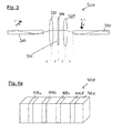
- a light integrator 100 shown schematically in side view has an integrator rod 101 of, for example, cuboid geometry with a light entry surface 102, a light exit surface 103 and four lateral surfaces 104-107, of which in FIG. 1 only the upper lateral surface 104, the lower lateral surface 105 and the front Lateral surface 106 can be seen.
- the integrator rod 101 is made of a material that is transparent to the respective working wavelength and can have any suitable cross section, preferably a rectangular or even square cross section, transverse to the light propagation direction or the optical axis.
- fluoride crystal materials such as calcium fluoride (CaF 2 ), barium fluoride (BaF 2 ), magnesium fluoride (MgF 2 ) or lithium fluoride (LiF 2 ) suitable.
- the light integrator 100 further has a dielectric layer system 108, which is applied uniformly and over the whole area in accordance with the exemplary embodiment of FIG. 1 on all lateral surfaces 104-107.
- the dielectric layer system is applied by means of a suitable method to the surface of the lateral surfaces 104-107, for example vapor-deposited, and consists, in an exemplary but not limiting embodiment, of a sequence of lanthanum fluoride (LaF 3 ) / chiolite layers according to Table 1a: ⁇ u> Table 1a: ⁇ / u> Layer no.
- the optical constants at a working wavelength of about 193 nm are shown in Table 1b, the values depending on the coating parameters subject to the usual fluctuations.
- n or k indicate the real or the imaginary part of the complex refractive index.
- the refractive index n of calcium fluoride (CaF 2 ), from which according to the embodiment the integrator rod is formed, is approximately n ⁇ 1.51 at the working wavelength of approximately 193 nm.
- Table 1b ⁇ / u> material n K LaF 3 1.67 0.0002 Chiolith 1:36 0.0004
- the dielectric layer system according to the first embodiment has a first dielectric material (LaF 3 ) with a refractive index n 1 greater than the refractive index n of the material of the integrator rod (CaF 2 ) and a second dielectric material (chiolith) with a refractive index n 2 smaller than the refractive index n of the material of the integrator rod.
- a suitable dielectric layer system consists of a sequence of lanthanum fluoride (LaF 3 ) / magnesium fluoride (MgF 2 ) layers, as defined in Table 2a. ⁇ u> Table 2a: ⁇ / u> Layer no. Physical thickness [nm] material air 1 61.4 LaF 3 2 53.5 MgF 2 3 57.5 LaF 3 4 40.7 MgF 2 5 43.0 LaF 3 6 56.6 MgF 2 7 20.0 LaF 3 substratum CaF 2
- a suitable dielectric layer system consists of a sequence of neodymium fluoride (NdF 3 ) / chiolite layers as defined in Table 3a. ⁇ u> Table 3a: ⁇ / u> Layer no. Physical thickness [nm] material air 1 48.6 NdF 3 2 48.7 Chiolith 3 22.4 NdF 3 substratum CaF 2
- the dielectric layer system preferably comprises at least two different dielectric materials, of which one material has a refractive index n 1 which is greater than the refractive index n of the material of the integrator rod, and the second dielectric material has a second refractive index n 2 which is less than the refractive index n of the material of the integrator rod is.
- the first dielectric material (having a refractive index n 1 greater than the refractive index n of the material of the integrator rod) may be selected from the group consisting of lanthanum fluoride (LaF 3 ), neodymium fluoride (NdF 3 ), Alumina (Al 2 O 3), gadolinium fluoride (GdF 3), dysprosium fluoride (DyF 3), erbium fluoride (ErF 3) and zirconium fluoride (ZrF 4).
- LaF 3 lanthanum fluoride
- NdF 3 neodymium fluoride
- Alumina Al 2 O 3
- gadolinium fluoride Gadolinium fluoride
- DyF 3 dysprosium fluoride
- ErF 3 erbium fluoride
- ZrF 4 zirconium fluoride
- the second dielectric material (with a refractive index n 2 smaller than the refractive index n of the material of the integrator rod) may in particular be selected from the group consisting of chiolite, magnesium fluoride (MgF 2 ), lithium fluoride (LiF), sodium fluoride (NaF), silicon dioxide ( SiO 2 ), cryolite and aluminum fluoride (AlF 3 ).
- the layer system 108 arranged on the lateral surfaces 104-107 of the integrator rod 101 is configured such that for a light beam reflected in the region of the lateral surface occupied by the layer system 108, a phase split (phase jump) of 180 ° between the perpendicular to the plane of incidence oriented component E s of the electric field vector and the parallel to the plane of incidence oriented component E p of the electric field vector takes place.
- a light integrator 200 shown schematically in side view has in another embodiment an integrator rod 201 of, for example, a cuboid geometry with a light entrance surface 202, a light exit surface 203 and four lateral surfaces 204-207, of which only the upper lateral surface in FIG 204, the lower lateral surface 205 and the front lateral surface 206 can be seen.
- an integrator rod 201 of, for example, a cuboid geometry with a light entrance surface 202, a light exit surface 203 and four lateral surfaces 204-207, of which only the upper lateral surface in FIG 204, the lower lateral surface 205 and the front lateral surface 206 can be seen.
- the lateral surfaces 204-207 are each covered with an optical retarder 208, which is produced from a suitable birefringent material with a suitable layer thickness such that it forms a lambda / 4 plate, which according to the exemplary embodiment is applied to all lateral surfaces 204-4. 207 evenly and over the entire surface by means of a suitable method applied (eg sprinkled) is.
- the lambda / 4 plate may be made of a suitable birefringent material, for example, for a working wavelength of 193 nm of magnesium fluoride (MgF 2 ) or quartz (SiO 2 ).
- the orientation of the fast is indicated in FIG. 2 by means of the auxiliary bar 209.
- the lambda / 4 plate located on the lateral surface has the consequence that between two consecutive total reflections on lateral surfaces, which are occupied by the lambda / 4 plate, a light beam passing through the integrator bar twice the thickness of the Lambda / 4 plate passes through, thus a total of two consecutive total reflections as it crosses a lambda / 2 plate.
- the lambda / 4 plate which has been passed twice in the light path between two total reflections, causes lambda / 2 phase splitting of this light beam after the double passage of a light beam, ie a 180 ° phase splitting between the component E s of the electric field vector oriented perpendicular to the plane of incidence parallel to the plane of incidence oriented component E p of the electric field vector.
- a light integrator 300 shown schematically in side view has, in a further exemplary embodiment, a second integrator rod 320 in addition to a first integrator rod 310, wherein the second integrator rod 320 has a substantially identical coverage of its lateral surfaces as the first integrator rod 310 and substantially identical Dimensions.
- the integrator rods 310, 320 may, for example, have the structure shown in FIG. 1 or also in FIG. 2, so that their detailed description is omitted here, wherein all other suitable embodiments of the integrator rods 310, 320 according to the invention are also suitable.
- a lambda / 2 retarder 340 is arranged such that light passing through the light integrator 300 successively passes through the first integrator rod 310, the lambda / 2 retarder 340, and the second integrator rod 320.
- positive lenses 330 and 350 are also provided in the beam path, with the lens 330 between the light exit surface of the first integrator rod 310 and the lambda / 2 retarder 340, and the lens 350 between the lambda / 2 retarder 340 and the light entry surface of the second integrator rod 320 is arranged.
- the lenses 330 and 350 may also be configured as multi-lens lens systems.
- Lens 330 establishes an as vertical as possible incidence of the light rays which have passed through the light integrator 310 when hitting the lambda / 2 retarder 340, for which purpose the light exit surface of the first integrator rod 310 is arranged at a distance of the focal length f from the lens 330.
- Lens 350 couples light rays passing through the light integrator 300 into the second Integratorstab 320, the light entrance surface is arranged at a distance of the focal length f of the lens 350.
- the invention is not limited to the uniform and all-over coverage of the lateral surfaces of the integrator rod or the integrator rods.
- the occupation of the respective lateral surface with the dielectric layer system or the optical retarder can also be provided, for example, only on two mutually opposite lateral surfaces of the integrator rod.
- the occupation of the respective lateral surface with the dielectric layer system or the optical retarder may, for example, also be provided only in regions, as will be explained by way of example only and not by way of limitation with reference to the exemplary embodiments shown in FIG.
- the light integrator 400 shown in FIG. 4a has an integrator rod 401, the lateral surfaces of which are only provided with a dielectric layer system in substantially uniformly spaced along the longitudinal direction, preferably strip-shaped regions 402a-402d. Analogous to FIG. 2, the strip-shaped regions 402a-402d can also be covered with a lambda / 4 plate.
- a 180 ° phase split occurs here between the component E s of the electric field vector oriented perpendicular to the plane of incidence and the component E p of the electric field vector oriented parallel to the plane of incidence not at every total reflection, but only after one Plurality of total reflections.
- the only partially occupancy of the lateral surfaces has the advantage that taking place in the occupied areas of the lateral surfaces decrease in reflectivity is reduced. Since a decrease in the reflectivity can in turn result in an increased ellipticity due to different number of total reflections in the x or y direction, in the case of (for example, according to FIG. 4 a), only partially covered lateral surfaces are counteracted by an undesired increase in ellipticity.
- This "ellipticity” is based on the intensity distribution resulting from the rod after light emission and results from the fact that the rays passing through the respective rod are reflected at the broad lateral surfaces more frequently than at the narrow lateral surfaces, so that in connection with the absorbing effect the dielectric layers give different attenuations of the beams and consequently the intensity in the horizontal direction differs from the intensity in the vertical direction.
- the value E (H, V) of the ellipticity designates the ratio of the sum of the intensities in the vertically opposite quadrants for two pairs of point-symmetrical to the optical axis in the vertical direction or horizontal direction opposite quadrants in the pupil the sum of the intensities in the horizontally opposite quadrants.
- a value E (H, V) 1 accordingly denotes a uniform intensity distribution in the pupil.
- the invention in the case of only partially occupying the outer surfaces with a dielectric layer system or an optical retarder is not limited in number or geometry of the occupied areas, but these can be in any suitable number and shape (possibly. matched to light source or the illumination setting used), both on be provided on all lateral surfaces and only on two opposite lateral surfaces.
- each of the light integrator also comprises two sub-rods
- all of these embodiments are characterized by only a partial occupancy of the lateral surfaces with a dielectric layer system.
- a lambda / 2 retarder may also be arranged between the two sub-rods as described above, but the two sub-rods of FIG. 4b-d may also be provided for manufacturing reasons (and without lambda / 2 retarder).
- only a partial occupancy of the lateral surfaces with a dielectric layer system can also take place in a light integrator with only one rod (analogous to FIG. 1), which then, for example, corresponds to the respective first rod in the embodiment shown in FIG. 4b.
- the configurations shown may be double (eg, to obtain the same homogenizing effect as one of the rods of the configurations shown in Figures 4b-d).
- the blank lateral surfaces are marked white, and the occupied lateral surfaces (regions 410a in FIGS. 4b, 430a in FIGS. 4b and 450a and 460a in FIG. 4d) are each marked gray.
- the partial bars 410, 420, 430, 440, 450 and 460 each have a cuboid geometry, wherein the aspect ratio of the rectangular bar cross-section perpendicular to the along the z-direction extending light propagation direction (defined as the ratio of height or smaller side length to width or larger page length) as well as in the preceding embodiments, for example, in the range of 1: 1 to 1: 8 may be.
- FIG. 4b and 4c show configurations in which only the narrow lateral surfaces of the first rod 430 and 450, respectively, in relation to the light propagation direction are covered with a dielectric layer, this covering being shown completely in FIG. 4c and half in FIG. 4b (in FIG along the light propagation direction first traversed area 430a of the first rod 430) takes place.
- FIG. 4d in addition to a complete occupancy of the narrow lateral surfaces 450a of the first rod 450, half the occupancy of the second rod 460 (likewise in the region 460a of the second rod 460 initially passed along the direction of light propagation) takes place.
- the invention is also not limited to the configurations shown in terms of occupying only in regions, so that the respective occupied areas can vary in size and arrangement.
- the ellipticity of the intensity distribution introduced by the occupation of the narrow lateral surfaces according to FIG. 4b-d can also be compensated for by an additional occupation of the broad lateral surfaces.
- the occupancy ratio which is defined as the ratio of the occupied surface of the narrow lateral surfaces to the occupied surface of the broad lateral surface of the respective rod, the aspect ratio of this Integratorstabes (ie the ratio of height or smaller side length to width or greater side length ).
- the occupancy ratio can also be selected slightly larger (eg, by a few percent) than the aspect ratio, in order to also reduce any compensate for ellipticity in the intensity distribution introduced by blank surfaces.
- a suitable Elliptizticiansfilters in the form of a transmission filter with a twofold symmetry is carried out according to the invention in connection with the partial occupancy of the Stabmantel vom described above WO 2005/006079 A1 is known.
- a transmission filter can be designed, for example, according to FIG. 4e in the form of a disk-shaped filter element 480, on which a plurality of surfaces with different degrees of transmission are arranged in a segment-like manner.
- the transmission filter 480 is subdivided, for example, into four quadrants 481-484 arranged point-symmetrically with respect to the central axis, of which two quadrants opposite the central axis or the optical system axis form a pair with the same transmittance and of which, for example, the one pair 482, 484 Transmittance of approximately 100% and the other pair 481, 483 may have a lower transmittance (of eg 90%).
- the ellipticity filter can be arranged in a lighting system whose structure is explained in more detail below with reference to FIG. 9, for example in a pupil plane of the REMA objective, and then serves to at least illuminate the ellipticity of the intensity distribution introduced by the (partial) dielectric coverage of the lateral surfaces partially correct.
- Table 4 indicates for the configurations of Fig. 4b-d the respectively calculated, expected values for the relative IPS increase, the ellipticity and the relative transmission (compared to a configuration without occupying the lateral surfaces), the reflectivity of with dielectric Layer occupied shell surfaces to 98% and the reflectivity unoccupied lateral surfaces was assumed to be 99.8%.
- the relative IPS increase denotes the relative gain of the IPS value compared to the analog configuration without covering the lateral surfaces.
- one in the integrator bar may e.g. ellipticity of the intensity distribution introduced by the occupancy of the narrow lateral surfaces according to FIG. 4b-d can also be compensated for by a contribution to the ellipticity of the intensity distribution introduced elsewhere in the illumination system.
- a contribution results, for example, from antireflective layers or layer systems (AR layers) present on the lenses of the illumination system, as well as from highly reflective layers or layer systems (HR layers) present on mirrors, where it has been found that e.g. AR layers may cause an ellipticity offset of the intensity distribution of greater than 5% using linearly polarized light of uniform linear polarization preferential direction using a lighting setting (e.g., C-quad setting).
- AR layers antireflective layers or layer systems
- HR layers highly reflective layers or layer systems
- linearly polarized light can be irradiated into the illumination system approximately in the x-direction (perpendicular to the scanning direction).
- the totality of AR layers and HR layers on the existing in the illumination system lenses or mirrors generates an ellipticity E (HV) ⁇ 1. This is due to the polarization-dependent transmission to said layers, which is based on the fact that s-polarized light reflects better each p-polarized light.
- the dielectric coverage of the narrow rod lateral surfaces produces an inverse effect on the E (HV) value, since the light is attenuated more strongly as a result of the respective occupation of the narrow lateral surfaces in the x-segments of the pupil than in the y-segments.
- FIG. 5 shows a simulation of the calculated dependence of the average linear polarization degree P at the rod exit on the parameter ⁇ , which indicates the numerical aperture normalized to the maximum system aperture at the rod entry.
- the light at the rod entrance is linearly polarized to 100% in the y-direction, ie at the rod entry a linear degree of polarization of One has.
- the phase splitting (FIG. 7a) is between the component E s oriented perpendicular to the plane of incidence and the component E p oriented parallel to the plane of incidence as well as the reflectance (FIG. 7b).
- the dependence of the phase jump occurring at total reflection on the lateral surfaces of the angle of incidence for a light integrator with lateral surfaces without occupancy according to the invention is shown in FIG.
- values of the phase splitting between the component E s of the electric field vector oriented perpendicular to the plane of incidence and the component Ep oriented parallel to the plane of incidence can be determined reach the electric field vector of about 140 °, the values reach the ideal value of 180 ° in part, or lie only a few degrees below.
- the reflectance of these design examples of dielectric layer systems, in the incident angle range of about 60 ° to 85 °, above 96%.
- the occupation of lateral surfaces of the rod integrator according to the invention can also take place with the objective of taking phase jumps between the element E s of the electric field vector oriented perpendicular to the plane of incidence and the component E p of the plane oriented parallel to the plane of incidence at the respective total reflections to minimize the electric field vector.
- FIG. 8 shows a simulation of the dependence of the phase splitting (FIG. 8a) and the reflectance (FIG. 8b) on the angle of incidence for such a light integrator with an integrator rod made of CaF 2 without or with coating with the layer structure according to the invention in the angle of incidence range of FIG 65 ° to 90 °.
- FIG. 9 shows a schematic representation of the structure of a lighting system of a microlithographic projection exposure apparatus with a light integrator according to the present invention.
- an illumination system 10 includes a light source 11 (for example, an ArF laser for an operating wavelength of 193 nm or an F 2 laser for an operating wavelength of 157 nm), a collector unit 12, a light integrator 13 and a REMA objective 14 on.
- the collector unit 12 focuses light coming from the light source 11 onto the light integrator 13.
- the light integrator has a structure as described above with reference to exemplary embodiments.
- the quality of polarization maintenance can vary over the pupil plane of the REMA objective 14, according to a preferred embodiment of the invention for improving the average polarization preservation, the use of a special diaphragm, which comparatively filtered out poor polarized areas and whose design is predetermined by the geometry of the integrator rod.
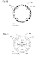
- a suitable embodiment of a diaphragm is shown in FIG. 10.
- This diaphragm 500 has on an outer ring 510 a plurality of radially inwardly projecting, light-blocking projections 520, which have a substantially serrated geometry ("spikes"), wherein they taper in the radial direction from outside to inside or pointed
- the opening angle of these serrated protrusions 520 may typically be in the range of about 1-5 °.
- the position of these inwardly projecting protrusions 520 around the periphery of the ring 510 is selected so that the protrusions 520 filter out the light at the pupil locations where the polarization is maximally disturbed by the rod geometry so that this light does not contribute to the mean polarization retention contributes so that the average polarization preservation is improved.
- the positions and dimensions of the radial projections 520 are predetermined by the geometry of the light integrator 13 (aspect ratio and length). For suitable design of the diaphragm 500, for example by means of the polarization measuring device 16 the degree of polarization at different field points in the reticle plane 15 are measured in order to determine where the areas of relatively poor polarization preservation (poor IPS value) lie for the specific light integrator 13 used, and then filter them out with the correspondingly produced aperture 500.
- Typical radial dimensions of the projections 520 are approximately in the range of 1/10 to 1/5 of the total radius of the ring 510.
- This total radius can be suitably selected depending on the location in the illumination device and is in the case of the preferred use in the pupil plane of the REMA objective 14 at about 100 mm.
- Aperture 500 in the embodiment shown in FIG. 10 is suitable for a configuration in which the azimuthal angles along the positive and negative x and y directions, respectively, have a relatively good polarization preservation, but positions that are relatively polarized are offset azimuthally at an angle of 45 ° or an integer multiple thereof on the positive y-axis, have a relatively poorer polarization retention.
- the diaphragm can also be arranged in front of the light integrator 13 relative to the light propagation direction, for example in a pupil plane of the collector unit 12.
- the radius of the ring 510 is to be adapted accordingly and is typically of the order of about 50 mm.
- FIG. 11 A further embodiment of a diaphragm for improving the average polarization retention is shown in FIG. 11.
- This diaphragm 600 also has a ring 610 provided with radially inwardly projecting protrusions 620 and differs from the diaphragm 500 of Fig. 11 in that in areas 630a, 630c surrounded by the ring two are mutually opposed are arranged opposite, plane-parallel plate elements 611, 612, each causing a rotation of the polarization direction of linearly polarized light by 90 ° or an odd multiple thereof.
- These plate elements 611, 612 may be formed, for example, of optically active material in the form of crystalline quartz, the optical crystal axis being oriented parallel to the z-axis extending in the light propagation direction. According to an alternative embodiment, these plate elements 611, 612 may also be configured in the form of lambda / 2 plates (for example made of MgF 2 or another suitable, sufficiently transparent material). In the diaphragm of FIG. 11, therefore, for entering light which is linearly polarized in the y direction in the regions 630a and 630c, a rotation of the polarization preferred direction by 90 ° (or an odd multiple thereof) takes place. In the other areas 630b and 630d, which are not filled with material according to the example of FIG.
- the diaphragm 600 thus additionally effects the generation of a "quasi-tangential" polarization distribution in addition to the above-described filtering of undesired regions with relatively poor polarization preservation, as indicated by the double arrows characterizing the polarization preferred direction produced after the diaphragm 600.
- plane-parallel plate elements of optically active material in the form of crystalline quartz may also be arranged for the same purpose, wherein the optical crystal axis in these plate elements is oriented parallel to the z-axis extending in the light propagation direction, and the thickness is selected is that for entering, in the y-direction linearly polarized light in the areas 630 b and 630 d rotation the polarization preferred direction by 180 ° (or an even multiple thereof) results.
- FIG. 12 shows a schematic representation of the structure of a microlithographic projection exposure apparatus with an illumination system according to the present invention.
- a microlithographic projection exposure apparatus 50 has a light source 51, an illumination system 52, a mask (reticle) 53, a mask carrier unit 54, a projection objective 55, a photosensitive structures substrate 56 and a substrate carrier unit 57.
- the illumination system 52 is designed in accordance with FIG. 9 and has a light integrator according to the invention.
- the image of the mask 13 illuminated by the illumination system 52 is projected by means of the projection lens 55 onto the substrate 56 (eg a silicon wafer) coated with a photosensitive layer (photoresist) and arranged in the image plane of the projection objective 55 in order to project the mask structure onto the photosensitive coating of the substrate 56.
- the substrate 56 eg a silicon wafer
- a photosensitive layer photoresist
Applications Claiming Priority (1)
| Application Number | Priority Date | Filing Date | Title |
|---|---|---|---|
| US68460205P | 2005-05-25 | 2005-05-25 |
Publications (2)
| Publication Number | Publication Date |
|---|---|
| EP1726994A2 true EP1726994A2 (fr) | 2006-11-29 |
| EP1726994A3 EP1726994A3 (fr) | 2007-08-08 |
Family
ID=36764284
Family Applications (1)
| Application Number | Title | Priority Date | Filing Date |
|---|---|---|---|
| EP06114425A Withdrawn EP1726994A3 (fr) | 2005-05-25 | 2006-05-23 | Intégrateur de lumière pour un système d'éclairage, en particulier pour une installation d'éclairage de projection microlithographique |
Country Status (1)
| Country | Link |
|---|---|
| EP (1) | EP1726994A3 (fr) |
Cited By (3)
| Publication number | Priority date | Publication date | Assignee | Title |
|---|---|---|---|---|
| WO2007039519A1 (fr) * | 2005-10-04 | 2007-04-12 | Carl Zeiss Smt Ag | Dispositif et procede permettant d'agir sur la distribution de la polarisation dans un systeme optique, notamment dans une installation d'eclairage par projection microlithographique |
| DE102019202752A1 (de) * | 2019-02-28 | 2020-01-02 | Carl Zeiss Smt Gmbh | Optisches system, blende und lithographieanlage |
| CN113205899A (zh) * | 2021-04-25 | 2021-08-03 | 中国工程物理研究院激光聚变研究中心 | 一种x射线折射闪耀光栅及制备方法 |
Citations (4)
| Publication number | Priority date | Publication date | Assignee | Title |
|---|---|---|---|---|
| WO2003077011A1 (fr) | 2002-03-14 | 2003-09-18 | Carl Zeiss Smt Ag | Systeme optique a elements optiques birefringents |
| DE10229614A1 (de) | 2002-06-25 | 2004-01-15 | Carl Zeiss Smt Ag | Katadioptrisches Reduktionsobjektiv |
| DE10240598A1 (de) | 2002-08-27 | 2004-03-25 | Carl Zeiss Smt Ag | Optisches Abbildungssystem, insbesondere katadioptrisches Reduktionsobjektiv |
| WO2005006079A1 (fr) | 2003-07-07 | 2005-01-20 | Carl Zeiss Smt Ag | Dispositif d'eclairage d'une installation d'eclairage de projection microlithographique |
Family Cites Families (2)
| Publication number | Priority date | Publication date | Assignee | Title |
|---|---|---|---|---|
| US5059917A (en) * | 1990-04-20 | 1991-10-22 | Hughes Aircraft Company | Optical phase conjugation apparatus including light pipe for multiple beam combination |
| US5748376A (en) * | 1996-04-17 | 1998-05-05 | Industrial Technology Research Institute | High optical throughput liquid-crystal projection display system |
-
2006
- 2006-05-23 EP EP06114425A patent/EP1726994A3/fr not_active Withdrawn
Patent Citations (6)
| Publication number | Priority date | Publication date | Assignee | Title |
|---|---|---|---|---|
| WO2003077011A1 (fr) | 2002-03-14 | 2003-09-18 | Carl Zeiss Smt Ag | Systeme optique a elements optiques birefringents |
| DE10311809A1 (de) | 2002-03-14 | 2003-10-02 | Zeiss Carl Smt Ag | Polarisationsoptimiertes Beleuchtungssystem |
| DE10229614A1 (de) | 2002-06-25 | 2004-01-15 | Carl Zeiss Smt Ag | Katadioptrisches Reduktionsobjektiv |
| DE10240598A1 (de) | 2002-08-27 | 2004-03-25 | Carl Zeiss Smt Ag | Optisches Abbildungssystem, insbesondere katadioptrisches Reduktionsobjektiv |
| WO2004025370A1 (fr) | 2002-08-27 | 2004-03-25 | Carl Zeiss Smt Ag | Systeme de reproduction optique, en particulier objectif de projection catadioptrique |
| WO2005006079A1 (fr) | 2003-07-07 | 2005-01-20 | Carl Zeiss Smt Ag | Dispositif d'eclairage d'une installation d'eclairage de projection microlithographique |
Cited By (5)
| Publication number | Priority date | Publication date | Assignee | Title |
|---|---|---|---|---|
| WO2007039519A1 (fr) * | 2005-10-04 | 2007-04-12 | Carl Zeiss Smt Ag | Dispositif et procede permettant d'agir sur la distribution de la polarisation dans un systeme optique, notamment dans une installation d'eclairage par projection microlithographique |
| US8077289B2 (en) | 2005-10-04 | 2011-12-13 | Carl Zeiss Smt Gmbh | Device and method for influencing the polarization distribution in an optical system |
| DE102019202752A1 (de) * | 2019-02-28 | 2020-01-02 | Carl Zeiss Smt Gmbh | Optisches system, blende und lithographieanlage |
| CN113205899A (zh) * | 2021-04-25 | 2021-08-03 | 中国工程物理研究院激光聚变研究中心 | 一种x射线折射闪耀光栅及制备方法 |
| CN113205899B (zh) * | 2021-04-25 | 2023-02-28 | 中国工程物理研究院激光聚变研究中心 | 一种x射线折射闪耀光栅及制备方法 |
Also Published As
| Publication number | Publication date |
|---|---|
| EP1726994A3 (fr) | 2007-08-08 |
Similar Documents
| Publication | Publication Date | Title |
|---|---|---|
| WO2005059653A2 (fr) | Dispositif de temporisation ayant un effet optique de polarisation et dispositif d'eclairage de projection microlithographique comportant un tel dispositif de temporisation | |
| DE102006030757A1 (de) | Polarisationsoptimiertes Beleuchtungssystem | |
| EP1260835B1 (fr) | Filtre pour l'atténuation de rayons ultraviolets | |
| WO2005085955A2 (fr) | Dispositif de filtre de transmission | |
| EP1130470A2 (fr) | Illumination de projection microlithographique avec polarisation tangentielle | |
| DE102008054582A1 (de) | Mikrolithographische Projektionsbelichtungsanlage | |
| DE102010029905A1 (de) | Optisches System einer mikrolithographischen Projektionsbelichtungsanlage | |
| DE102007042047A1 (de) | Teilsystem einer Beleuchtungseinrichtung einer mikrolithographischen Projektionsbelichtungsanlage | |
| WO2007039519A1 (fr) | Dispositif et procede permettant d'agir sur la distribution de la polarisation dans un systeme optique, notamment dans une installation d'eclairage par projection microlithographique | |
| DE102007010650A1 (de) | Beleuchtungseinrichtung einer mikrolithographischen Projektionsbelichtungsanlage | |
| EP1474726A2 (fr) | Systeme d'eclairage a polarisation optimisee | |
| DE102008040058B4 (de) | Mikrolithographische Projektionsbelichtungsanlage und Verfahren zur mikrolithographischen Herstellung mikrostrukturierter Bauelemente | |
| WO2004102224A2 (fr) | Systeme axiconique et systeme d'eclairage equipe de ce dernier | |
| EP1726994A2 (fr) | Intégrateur de lumière pour un système d'éclairage, en particulier pour une installation d'éclairage de projection microlithographique | |
| WO2007025783A2 (fr) | Systeme microlithographique d'eclairage par projection | |
| WO2006131517A2 (fr) | Dispositif d'eclairage pour un systeme d'eclairage par projection pour la microlithographie | |
| DE102011003035A1 (de) | Polarisationsbeeinflussende optische Anordnung, sowie optisches System einer mikrolithographischen Projektionsbelichtungsanlage | |
| EP1754111A1 (fr) | Systeme d'eclairage d'un dispositif d'eclairage par projection micro-lithographique | |
| DE102007055063A1 (de) | Beleuchtungseinrichtung einer mikrolithographischen Projektionsbelichtungsanlage | |
| DE102017209162A1 (de) | Retardierungselement, sowie optisches System | |
| EP2041625A1 (fr) | Systeme d'eclairage d'un equipement d'eclairage par projection microlithogafique | |
| WO2010034367A1 (fr) | Miroir diélectrique et son procédé de fabrication ainsi qu'une installation d'exposition par projection pour la microlithographie avec un miroir de ce type | |
| WO2020083543A1 (fr) | Système optique, en particulier pour la microlithographie | |
| DE102012217769A1 (de) | Optisches System für eine mikrolithographische Projektionsbelichtungsanlage sowie mikrolithographisches Belichtungsverfahren | |
| DE10338983A1 (de) | Projektionsobjektiv für die Mikrolithografie |
Legal Events
| Date | Code | Title | Description |
|---|---|---|---|
| PUAI | Public reference made under article 153(3) epc to a published international application that has entered the european phase |
Free format text: ORIGINAL CODE: 0009012 |
|
| AK | Designated contracting states |
Kind code of ref document: A2 Designated state(s): AT BE BG CH CY CZ DE DK EE ES FI FR GB GR HU IE IS IT LI LT LU LV MC NL PL PT RO SE SI SK TR |
|
| AX | Request for extension of the european patent |
Extension state: AL BA HR MK YU |
|
| PUAL | Search report despatched |
Free format text: ORIGINAL CODE: 0009013 |
|
| AK | Designated contracting states |
Kind code of ref document: A3 Designated state(s): AT BE BG CH CY CZ DE DK EE ES FI FR GB GR HU IE IS IT LI LT LU LV MC NL PL PT RO SE SI SK TR |
|
| AX | Request for extension of the european patent |
Extension state: AL BA HR MK YU |
|
| AKX | Designation fees paid | ||
| STAA | Information on the status of an ep patent application or granted ep patent |
Free format text: STATUS: THE APPLICATION IS DEEMED TO BE WITHDRAWN |
|
| 18D | Application deemed to be withdrawn |
Effective date: 20080209 |
|
| REG | Reference to a national code |
Ref country code: DE Ref legal event code: 8566 |