EP1724936A2 - Matching circuit - Google Patents
Matching circuit Download PDFInfo
- Publication number
- EP1724936A2 EP1724936A2 EP06010268A EP06010268A EP1724936A2 EP 1724936 A2 EP1724936 A2 EP 1724936A2 EP 06010268 A EP06010268 A EP 06010268A EP 06010268 A EP06010268 A EP 06010268A EP 1724936 A2 EP1724936 A2 EP 1724936A2
- Authority
- EP
- European Patent Office
- Prior art keywords
- matching
- matching block
- circuit
- block
- auxiliary
- Prior art date
- Legal status (The legal status is an assumption and is not a legal conclusion. Google has not performed a legal analysis and makes no representation as to the accuracy of the status listed.)
- Withdrawn
Links
Images


Classifications
-
- H—ELECTRICITY
- H04—ELECTRIC COMMUNICATION TECHNIQUE
- H04B—TRANSMISSION
- H04B1/00—Details of transmission systems, not covered by a single one of groups H04B3/00 - H04B13/00; Details of transmission systems not characterised by the medium used for transmission
- H04B1/38—Transceivers, i.e. devices in which transmitter and receiver form a structural unit and in which at least one part is used for functions of transmitting and receiving
- H04B1/40—Circuits
- H04B1/44—Transmit/receive switching
-
- H—ELECTRICITY
- H03—ELECTRONIC CIRCUITRY
- H03H—IMPEDANCE NETWORKS, e.g. RESONANT CIRCUITS; RESONATORS
- H03H7/00—Multiple-port networks comprising only passive electrical elements as network components
- H03H7/38—Impedance-matching networks
- H03H7/383—Impedance-matching networks comprising distributed impedance elements together with lumped impedance elements
-
- H—ELECTRICITY
- H04—ELECTRIC COMMUNICATION TECHNIQUE
- H04B—TRANSMISSION
- H04B1/00—Details of transmission systems, not covered by a single one of groups H04B3/00 - H04B13/00; Details of transmission systems not characterised by the medium used for transmission
- H04B1/02—Transmitters
- H04B1/04—Circuits
- H04B1/0458—Arrangements for matching and coupling between power amplifier and antenna or between amplifying stages
Definitions
- This invention pertains to a matching circuit handling multiple bands which, in a plurality of frequency bands, establishes matching between circuits having different impedances. It pertains to matching circuits built into small-sized multiband power amplifiers which amplify, with high efficiency, signals in a plurality of frequency bands used e.g. in mobile communications and satellite communications.
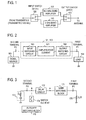
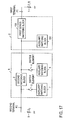
- the configuration of the 800 MHz/2 GHz band power amplifier shown in Reference 1 is shown in Fig. 1, and the operation thereof will be explained.
- the transmitted signal coming from the transmitter is input into the single pole terminal of an input switch 150, a Single Pole Double Throw (SPDT) switch.
- the transmitted signal by being switched by input switch 150, is input into an 800 MHz band amplifier 151 connected to a double throw terminal of input switch 150, or a 2 GHz band amplifier 152.
- the output signals of 800 MHz band amplifier 151 and 2 GHz band amplifier 152 are switched by an output switch 153, a Single Pole Double Throw switch, and supplied to an antenna.
- Fig. 2 the configuration of 800 MHz band amplifier 151 and 2 GHz band amplifier 152 is shown.
- Each amplifier is configured with a series connection of an input matching circuit 160, an amplification element 161, and an output matching circuit 162.
- Input matching circuit 160 obtains matching between a signal source 163, whose output impedance does not depend on the frequency, and amplification element 161.
- Output matching circuit 162 obtains matching between the output impedance of amplification element 161 and a load 164.
- the method of designing matching circuits for wideband operation can also be considered.
- the result is that there occurs a reduction in gain and efficiency.
- the applicant of the present application first proposed, in Reference 2 (International Publication No. WO 2004/082138 Pamphlet), a matching circuit which can handle the conversion to multiband capability.
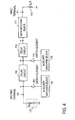
- the input matching circuit of the amplifier disclosed in Reference 2 is shown in Fig. 3.
- the FET (Field Effect Transistor) input impedance can be expressed as a load 170 (impedance Z L (f)) having frequency-dependent characteristics.
- a first terminal P1 to which this load 170 is connected has a main matching block 171 connected to it.
- the other end (point A) of main matching block 171 is connected to one end of a delay circuit 172 having a certain reactance value.
- the other end (point B) of delay circuit 172 is connected to a signal source 173 having an impedance Z0 (below, the impedance not changing with frequency is called Z0).
- Main matching block 171 is designed to match the impedance Z L (f1) of load 170 with the impedance Z0 of signal source 173, in frequency band f1. In other words, main matching block 171 becomes a matching circuit with respect to frequency f1.
- Delay circuit 172 is constituted by a distributed-parameter element, the characteristic impedance of which is given, as is well known, by the relationship shown in Eq. 1.
- Z 0 L / C
- L is the inductance of the distributed-parameter element and C is the capacitance of the distributed-parameter element. Consequently, by taking the characteristic impedance of delay circuit 172 to be Z0, matching is obtained in frequency band f1 between signal source 173 and load 170.
- the impedance of load 170 changes to Z L (f2).
- main matching block 171 is a matching circuit with respect to frequency f1
- matching between signal source 173 and load 170 is not obtained at frequency f2.
- an auxiliary matching block 175 is connected via switch element 174 to point B.
- switch element 174 is taken to be in a conducting state.
- the delay value of delay circuit 172 is set to the delay value required to match at point B in frequency band f2.
- a third frequency band f3 the impedance Z L (f3) of load 170 is regulated by means of delay circuit 180 and auxiliary matching block 182 so that the impedance seen from point C toward the side of delay circuit 180 becomes Z0.
- switch element 174 and switch element 181 are chosen to be in a non-conducting state in the case of frequency band f1
- switch element 174 is chosen to be in a conducting state for in the case of frequency band f2
- switch element 181 is chosen to be in a conducting state in the case of frequency band f3.
- the delay value required in frequency band f3 can be considered to be the sum of the values for delay circuit 172 and delay circuit 180.
- delay circuits 172 and 180 it is realistic to choose them to be transmission lines which are distributed parameter networks. However, particularly in cases where the frequency is low, transmission lines become comparatively large components inside the circuit. E.g., if load 170 is taken to be a FET and in case an amplifier for the 1 GHz band is designed, a 50 ⁇ transmission line has a width of 0.63 mm and a length of 9.22 mm, so the result is a component having a length of about 10 mm.
- the delay circuits are realistically constituted by transmission lines.
- the length easily becomes comparatively long.
- the area of a transmission line serving as a delay circuit becomes large, so there has been the problem that the matching circuit as a whole also was made bigger. Further, this problem increases as the frequency becomes lower, and as the number of frequencies rises.
- the matching circuit of the present invention has a first matching block, connected at one end to a load having an impedance with frequency-dependent characteristics and a second matching block formed by a lumped-parameter element connected in series to the first matching block.
- the second matching block matches the impedances of the signal source and the load in the lowest frequency band.
- it has a ⁇ -type circuit.
- a ⁇ -type circuit is a circuit in which respective switch elements and auxiliary matching blocks are connected to both ends of the second matching block.
- the matching conditions in the aforementioned low frequency band can be created by a series connection of the first matching block and the second matching block.
- the impedance of the ⁇ -type circuit in the case of a high frequency band, by setting an appropriate value for the ⁇ -type circuit, it is possible to choose the impedance of the ⁇ -type circuit to be Z0 and to choose the impedance of the second matching block to be one with no influence for the high frequency band.
- the second matching block is constituted by lumped elements, it is possible to make the matching circuit smaller-sized than the conventional matching circuit constituted by transmission lines.
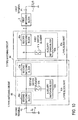
- the matching circuit of the present invention is constituted by a first matching block 2 and a matching circuit part 8 consisting of lumped elements.
- Matching circuit part 8 is a ⁇ -type circuit constituted by a second matching block 3, switch elements 4 and 5, and auxiliary matching blocks 6 and 7.
- One end of first matching block 2 is connected to a first terminal P1 to which an element 1 (a load in this example) having an impedance Z L (f) with frequency-dependent characteristics is connected.
- an element 1 a load in this example
- Z L (f) impedance Z L (f) with frequency-dependent characteristics
- matching circuit part 8 becomes a ⁇ -type circuit.
- Fig. 6A is a diagram showing the operation in a low frequency band f2.
- Fig. 6B is a diagram showing the operation in a high frequency band f1.
- switch elements 4 and 5 of Fig. 5 are non-conducting.
- impedance Z2 of the second matching block is set so that the sum Z A of impedance Z L (f2) of element 1 in the frequency band f2, impedance Z1 of first matching block 2, and impedance Z2 of second matching block 3 (below, the impedances will be omitted in portions where the same can be considered not to be particularly necessary) becomes Z0.
- the impedances are matched at second terminal P2.
- first matching block 2 is a matching circuit for the frequency band f1
- Z3 and Z4 may be designed so that the condition shown in Eq. 2 is met.
- Z ⁇ Z 0 Z 2 Z 3 + Z 4 Z 2 Z 3 + Z 0 Z 4 Z 3 / Z 0 Z 4 + Z 0 Z 2 + Z 0 Z 3 + Z 4 Z 2 + Z 1 Z 3
- first matching block 2 which operates to match impedance Z L (f1) of element 1 to impedance Z0 of element 9.
- second matching block 3 which operates to match the impedance Z L (f2) of element 1, changed by the modification of the frequency band from f1 to f2, to the impedance Z0 of element 9.
- auxiliary matching blocks 6 and 7 which operate to remove the influence of second matching block 3 which is a hindrance in frequency band f1.
- Matching circuit part 8 in Fig. 5 can also be configured with a T-type circuit.
- An example where the matching circuit part has been configured with a T-type circuit is shown in Fig. 7.
- second matching block 3 in Fig. 5 is replaced by a second matching block 31 and a series second matching block 32.
- One end of second matching block 31 is connected to point A.
- the other end of second matching block 31 is connected to one end of series second matching block 32.
- the other end of series second matching block 32 is connected to second terminal P2.
- an auxiliary matching block 34 via a switching element 33.
- Fig. 5 and Fig. 7 cannot be converted with the well known Y- ⁇ conversion (T- ⁇ conversion) relationship.
- the impedance value of auxiliary matching block 34 may be designed by adding this condition.
- matching block part 8 may be designed with a T-type circuit from the beginning. In this way, it is possible for matching circuit part 8 to have a configuration which is not limited to a ⁇ -type circuit but can also be a T-type circuit.
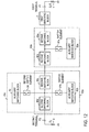
- Fig. 8 is an example where the basic structure of this invention, shown in Fig. 5, has been generalized so that it can be adapted to a plurality of frequency bands.
- This matching circuit is composed of first matching block 2, L-type blocks 43a to 43n, and shunt circuit blocks 46a to 46n.
- One terminal of second matching block 40a is connected to first matching block 2.
- the other end of second matching block 40a is connected to one terminal of second matching block 40b. In this way, each second matching block 40i is connected in series.
- First auxiliary matching block 42i is connected, via first switch element 41 i, to the terminal of second matching block 40i on the side of first terminal P1.
- an L-type circuit is formed by means of second matching block 40i, first switch element 41 i, and first auxiliary matching block 42i.
- first switch elements 41a to 41 c and second switch elements 44a to 44c are all in a non-conducting state.
- Element 1 is connected, via three second matching blocks 40a to 40c connected in series, to element 9 (impedance Z0).
- the impedance Z L (f) of element 1 changes with frequency.
- element 9 is a signal source or the like, the impedance of which does not depend on the frequency.
- second matching block 40c is designed so that the combined impedance of element 1, first matching block 2, and second matching blocks 40a and 40b is converted to Z0. If second matching block 40c is designed in this way, the impedance Z0 is matched at the second terminal P2 side end of second matching block 40c.
- switch element 41 c of L-type block 43c and second switch element 44a of shunt circuit block 46a are chosen to be in a conducting state.
- first auxiliary matching block 42c and second auxiliary matching block 45a are connected to both ends of second matching block 40c, a ⁇ -type circuit is configured.
- second matching block 40b is designed so that the combined impedance due to element 1 (impedance Z L (f3)), first matching block 2, and second matching block 40a is matched to Z0. If second matching block 40b is designed in this way, the impedance seen from the second terminal P2 side of second matching block 40b (the first tenninal P1 side of second matching block 40c) toward element 1 becomes Z0.
- first auxiliary matching block 42c and second auxiliary matching block 45a are designed so that Eq. 2 is satisfied at frequency f3.
- the impedance seen from the first terminal P1 side of second matching block 40c (the second terminal P2 side of second matching block 40b) toward element 9 also becomes Z0. In other words, it is possible to remove the influence of the impedance of second matching block 40c, so the impedances are matched.
- Second matching block 40a is designed so that the combined impedance due to element 1 (impedance Z L (f2)) and first matching block 2 is matched to Z0. If second matching block 40a is designed in this way, the impedance seen from the second terminal P2 side of second matching block 40a (the first terminal P1 side of second matching block 40b) toward element 1 becomes Z0.
- first auxiliary matching block 42b and second auxiliary matching block 45b are designed so that Eq. 2 is satisfied at frequency f2.
- the impedance seen from the first terminal P1 side of second matching block 40b (the second terminal P2 side of second matching block 40a) toward element 9 also becomes Z0. In other words, it is possible to remove the influence of second matching blocks 40b and 40c, so the impedances are matched.
- switch element 41a of L-type block 43a and second switch element 44c of shunt circuit block 46c are in a conducting state.
- first auxiliary matching block 42a and second auxiliary matching block 45c are connected to both ends of second matching blocks 40c to 40a, a ⁇ -type circuit is configured.
- First matching block 2 is designed so that impedance Z L (f1) of element 1 is matched to Z0. If first matching block 2 is designed in this way, the impedance seen from the second terminal P2 side of first matching block 2 (the first terminal P1 side of second matching block 40a) toward element 1 becomes Z0.
- first auxiliary matching block 42a and second auxiliary matching block 45c are designed so that Eq.
- Fig. 9 expresses the image of N frequency bands.
- the abscissa axis of Fig. 9 is the frequency and the ordinate axis is the power of transmission.
- a relation that the frequency becomes lower as N increases is shown as an example.
- the frequencies are arranged in the order corresponding to shunt circuit blocks 46a to 46n.
- the order of arranging shunt circuit blocks 46a to 46n is indifferent.
- the second matching block is configured with lumped elements connected in series between the conductively connected first switch element and second switch element. Consequently, even if the number of second matching blocks becomes large, it is possible to make the whole circuit remarkably small, compared to the case of a configuration with transmission lines.
- FIG. 10 there is shown an embodiment of a matching circuit using two T-type circuits.
- This matching circuit is composed of first matching block 2, an L-type block part 63a, an L-type block part 63b, and a second matching block 60c.
- One end of first matching block 2 is connected to a first terminal P1 at which it is connected to element 1.
- the other end of first matching block 2 is connected to one end of a second matching block 60a inside L-type block part 63a.
- second matching block 60a is also connected to one end of a second matching block 60b inside L-type block part 63b.
- an auxiliary matching block 62b is connected via a second switch element 61b.
- the other end of second matching block 60b is also connected to one end of second matching block 60c.
- L-type block part 63 a is composed of second matching block 60a, first switch element 61 a, and auxiliary matching block 62a.
- L-type block part 63b is composed of second matching block 60b, second switch element 61b, and auxiliary matching block 62b.
- T-type matching circuits 64 and 65 are composed of two L-type block parts 63a and 63b and one second matching block 60c.
- T-type matching circuit 64 is composed of second matching blocks 60a and 60b, first switch element 61 a, and auxiliary block 62a.
- T-type matching circuit 65 is composed of second matching blocks 60c and 60b, second switch element 61b, and auxiliary matching block 62b. In this way, a matching circuit which matches impedances in three frequency bands is configured in two stages with T-type matching circuits 64 and 65.
- switch elements 61a and 61b are chosen to be in a non-conducting state.
- the impedance of element 1 changes with the frequency band.
- Element 1 with an impedance Z L (f3) is connected, via the serially connected first matching block 2 and second matching blocks 60a, 60b, and 60c, to element 9 which has an impedance of Z0.
- Second matching block 60b and second matching block 60c are designed so that the combined impedance with element 1, first matching block 2, and second matching block 60a becomes Z0. By designing second matching block 60b and second matching block 60c in this way, it is possible to match the impedances at second terminal P2 of second matching block 60c.
- Second matching block 60a is designed so that the combined impedance with element 1, having an impedance Z L (f2), and first matching block 2 is taken to be Z0.
- auxiliary matching block 62b is designed so that the combined impedance of second matching blocks 60b and 60c, auxiliary matching block 62b, and element 9 becomes Z0. If auxiliary matching block 62b is designed in this way, the impedance seen from point D toward the element 9 side becomes Z0. Consequently, it is possible to match the impedances at point D.
- auxiliary matching block 62b removes the influence of second matching blocks 60c and 60b at frequency f2.
- switch element 61b constituting T-type matching circuit 65 is in a non-conducting state
- switch element 61a constituting T-type matching circuit 64 is in a conducting state.
- First matching block 2 is designed so that the the combined impedance with impedance Z L (f1) of element 1 becomes Z0. By designing first matching block 2 in this way, the impedance seen from point A toward element 1 becomes Z0.
- first auxiliary matching block 62a is designed so that the combined impedance of second matching blocks 60a, 60b, and 60c, auxiliary matching block 62a, and element 9 becomes Z0. By designing first auxiliary matching block 62a in this way, the impedance seen from point A toward element 9 becomes Z0.
- auxiliary matching block 62a removes the influence of second matching blocks 60a, 60b, 60c at the frequency f1.
- switch element 61b is non-conducting. However, it is not mandatory to take switch element 61 b to be non-conducting. In case switch element 61 b is taken to be conducting when the frequency band is f1, auxiliary matching block 62a may be designed with that assumption.
- FIG. 11 An example showing a generalization of the T-type matching circuit explained in Embodiment 3 is shown in Fig. 11.
- the configuration up to the second-stage L-type block 63b seen from first matching block 2 is identical to that of Fig. 10.
- L-type blocks are added on the second terminal P2 side of second-stage L-type block 63b.
- a total ofN L-type blocks 63a to 63n are connected.
- N is an integer equal to or greater than 1.
- the matching circuit shown in Fig. 11 is a subordinate connection configuration ofN T-type matching circuits and is capable of matching in N+1 frequency bands. The operation is the same as in Fig. 10.
- FIG. 12 Another T-type matching circuit embodiment is shown in Fig. 12.
- a T-type circuit was formed using second matching blocks of adjacent L-type blocks.
- Fig. 12 is an example in which a plurality of auxiliary matching blocks are connected, via switch elements, between two second matching blocks connected in series.
- This matching circuit is composed of first matching block 2 and T-type matching circuits 83a, 83b, and 83c.
- T-type matching circuit 83a is composed of second matching blocks 80a and 80b, a switch element 81a, and an auxiliary matching block 82a.
- One end of second matching block 80a is connected to first matching block 2.
- the other end of second matching block 80a is connected to one end of second matching block 80b.
- auxiliary matching block 82a is connected, via switch element 81a, between second matching block 80a and second matching block 80b.
- second matching blocks 80a and 80b, switch element 81 a, and auxiliary matching block 82a make up a T-type circuit.
- T-type matching circuit 83b is composed of second matching blocks 80c and 80d, a switching element 81b, and an auxiliary matching block 82b.
- T-type matching circuit 83c is composed of second matching blocks 80c and 80d, a second switching element 84, and an auxiliary matching block 85.
- second matching blocks 80c and 80d are constituent parts of both T-type matching circuit 83b and T-type matching circuit 83c.
- auxiliary matching block 82b is connected, via switch element 81b, to the connection point of second matching block 80c and second matching block 80d.
- auxiliary matching block 85 is also connected, via second switch element 84, to the connection point of second matching block 80c and second matching block 80d.
- One end of second matching block 80c is connected to second matching block 80b.
- the other end of second matching block 80d is connected to the second terminal P2 to which element 9 is connected.
- a T-type matching circuit may be connected in multiple stages between element 1 and element 9.
- the present embodiment is capable of matching in three frequency bands by means of three T-type matching circuits.
- Second matching blocks 80c and 80d are designed so that the combined impedance with element 1 (impedance Z L (f3)), first matching block 2, and second matching blocks 80a, 80b is made to match the impedance Z0 of element 9 in the frequency band f3. Consequently, impedance matching can be obtained at second terminal P2.
- Second matching blocks 80a and 80b are designed so that the combined impedance of element 1 (impedance Z L (f2)) and first matching block 2 is made to match the impedance Z0 of element 9 in the frequency band f2. Consequently, the impedance seen from the second terminal P2 side of second matching block 80b (the first terminal P1 side of second matching block 80c) toward element 1 becomes Z0. Also, auxiliary matching block 82b is designed so that the combined impedance of second matching blocks 80c and 80d, auxiliary matching block 82b, and element 9 becomes Z0 at the frequency f2.
- auxiliary matching block 82b By designing auxiliary matching block 82b in this way, the impedance seen from the first terminal P1 side of second matching block 80c (the second terminal P2 side of second matching block 80b) toward element 9 becomes Z0 at the frequency f2. Consequently, the impedances are matched.
- First matching block 2 is designed so that the impedance of element 1 (impedance Z L (f2)) is made to match the impedance Z0 of element 9 in the frequency band f1. Consequently, the impedance seen from the second terminal P2 side of first matching block 2 toward element 1 becomes Z0.
- Auxiliary matching block 82a and 85 are designed so that, in the frequency band f1, the combined impedance of second matching blocks 80a, 80b, 80c and 80d, auxiliary matching block 82a, and element 9 becomes Z0. Consequently, the impedance seen from the second terminal P2 side of first matching block 2 (the first terminal P1 side of second matching block 80a) toward element 9 becomes Z0.
- the two second matching blocks and the auxiliary matching block only make up a set with respect to one frequency band.
- a plurality of auxiliary matching blocks becomes necessary.
- Fig. 13 shows a configuration example of a matching circuit using an additional auxiliary matching block.
- Fig. 13 shows a configuration example where a second switch element 90 and a second auxiliary matching block 91 have been connected in series with auxiliary matching block 82b of Fig. 12. Having auxiliary matching blocks connected in series in two stages is done so that second matching blocks 80c and 80d constituting T-type matching circuit 83b can handle two frequency bands.
- switch element 81b may be configured with a Single Pole Double Throw (SPDT) switch or a multi-contact switch, and switching may be performed between auxiliary matching blocks with different values.
- SPDT Single Pole Double Throw
- the invention is not limited to the T type or the ⁇ type.
- Second matching block 3 is constituted by an L-type circuit consisting of a series matching block 100, a switch element 101 for matching, and a matching element 102.
- One end of series matching block 100 is connected to first matching block 2.
- Matching element 102 is connected to the other end of series matching block 100 via switch element 101 for matching.
- switch elements 4 and 5 are in a non-conducting state, and only switch element 101 for matching is conducting. At this point, the sum of the impedances of element 1 and first matching block 2 are matched to impedance Z0 of element 9 by means of series matching block 100 and matching element 102.
- switch elements 4 and 5 are made to conduct and switch element 101 for matching is chosen to be non-conducting.
- matching element 102 it is possible, by the existence of matching element 102, to broaden the options of second matching block 3 and auxiliary matching block 6 and 7.
- second matching block 3 it is possible to increase the freedom in designing second matching block 3 by configuring second matching block 3 with series matching block 100, first switch element 101 for matching, and matching element 102.
- the values of the lumped elements constituting second matching block 3 are discrete, making delicate tuning difficult.
- Second matching block 3 in Fig. 15 is constituted by a T-type circuit consisting of second matching blocks 60a and 60b, a switch element 110 for matching, and a matching element 111.
- Second matching block 60a and second matching block 60b are connected in series.
- One end of second matching block 60a is connected to first matching block 2.
- the other end of second matching block 60b is connected to second terminal P2.
- Matching element 111 is connected, via switch element 110 for matching, to the connection point of second matching block 60a and second matching block 60b.
- Switch element 110 for matching and matching element 111 are provided in order to increase the freedom in designing the second matching blocks and auxiliary matching block 7 and auxiliary matching block 6. Regarding the function, it is the same as in Embodiment 7.
- FIG. 16 differs from Fig. 7 in the point that, on the second terminal P2 side of T-type matching circuit part 30, there are provided a switch element 120 form matching and a matching element 121.
- switch element 33 and switch element 120 for matching are e.g. made to conduct exclusively.
- Matching element 121 and second matching block 31 and 32 are designed so that the combined impedance with element 1 and first matching block 2 is chosen to be Z0.
- first matching block 2 may also be configured with a plurality of elements.
- a configuration example thereof is shown in Fig. 17.
- first matching block 2 is composed of a first series matching block 130 and an auxiliary matching block 131 connected to one end thereof. Further, auxiliary matching block 131 may be connected to either end of first series matching block 130.
- First series matching block 130 is connected to element 9 via matching circuit part 8.
- any circuit configuration is acceptable.
- Fig. 18 is an example applied to an amplifying circuit operating in two frequency bands, the 2 GHz band and the 1 GHz band.
- FET 140 which is a power amplifier element
- the matching circuit shown in Fig. 17 is connected, and on the input side, the matching circuit shown in Fig. 16 is connected.
- first matching block 2 has become a first matching block 141.
- the output side matching circuit has, based on the matching circuit shown in Fig. 16, first matching block 2 configured with a first matching block 142.
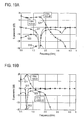
- Fig. 19A and Fig. 19B the simulation results for the amplifier in Fig. 18 are shown.
- Fig. 19A is a diagram showing the frequency characteristics in the case where the circuit has been set for the 2 GHz band.
- the abscissa axis indicates the frequency and the ordinate axis indicates the S parameter.
- the reflection S 11 of the signal input into first terminal P1 gets attenuated abruptly at 2 GHz.
- the transmission S 21 of the signal input in first terminal P1 exhibits a value of approximately 14 dB at 2 GHz, so the circuit transmits well.
- Fig. 19B is a diagram showing the frequency characteristics in the case where the circuit has been set for the 1 GHz band.
- the reflection S 11 of the signal input into first terminal P1 gets attenuated abruptly at 1 GHz.
- the transmission S 21 of the signal input in first terminal P1 exhibits a value of approximately 19 dB at 1 GHz, so the circuit transmits well. It is seen that the matching circuit according to the present invention functions as a multiband matching circuit.
- the matching circuit according to the present invention has an impedance seen from both ends of a second matching block, inserted between element 9 and element 1 and formed with lumped-parameter elements, which is made to match the impedance Z0 by means of an auxiliary matching block. Also, by raising the number of auxiliary matching blocks, a matching circuit handling a plurality of frequency bands is adopted. Further, since the second matching block is formed with lumped elements, it can be made smaller than prior-art matching circuits configured with transmission lines.
- Fig. 3 and Fig. 5 are diagrams of circuits made capable of matching in two frequency bands together.
- the matching circuit of the present invention (Fig. 5) requires in total two additional components, one switch element and one auxiliary matching circuit.
- the delay circuit 172 required in the conventional matching circuit is a large-size component.
- the size thereof varies with the frequency band and the used power amplification element, but when e.g., the frequency band is taken to be 1 GHz with a certain amplification element, the width is 0.63 mm and the length is 9.22 mm, or the length is 15.32 mm.
- the matching circuit of the present invention can be configured with a chip circuit commonly known by the name 0603 and having a width of 0.3 mm and a length of 0.6 mm and a Monolithic Microwave Integrated Circuit several mm square.
- all of the components constituting the matching circuit of the present invention end up amply fitting into the space of delay circuit 172.
- the number of delay circuits 172 must be increased. Consequently, as a matching circuit for multiband use, the matching circuit of the present invention can be further reduced in size, compared to a conventional matching circuit.
Landscapes
- Engineering & Computer Science (AREA)
- Computer Networks & Wireless Communication (AREA)
- Signal Processing (AREA)
- Amplifiers (AREA)
- Microwave Amplifiers (AREA)
- Transmitters (AREA)
Abstract
Description
- This invention pertains to a matching circuit handling multiple bands which, in a plurality of frequency bands, establishes matching between circuits having different impedances. It pertains to matching circuits built into small-sized multiband power amplifiers which amplify, with high efficiency, signals in a plurality of frequency bands used e.g. in mobile communications and satellite communications.
- Accompanying the diversification of services offered by means of radio communications, conversion to multiband capability for processing signals in a plurality of frequency bands is required of radio equipment. As an indispensable device included in radio equipment, there is the power amplifier. In order to carry out efficient amplification, there is a need to obtain impedance matching between the amplification element and its peripheral circuits, so a matching circuit is used. As an example of a conventional multiband power amplifier, technology as shown in Reference 1 (NTT DoCoMo Technical Journal, Vol. 10, No. 1: "Mobile Handsets") is disclosed.
- The configuration of the 800 MHz/2 GHz band power amplifier shown in
Reference 1 is shown in Fig. 1, and the operation thereof will be explained. The transmitted signal coming from the transmitter is input into the single pole terminal of aninput switch 150, a Single Pole Double Throw (SPDT) switch. Next, the transmitted signal, by being switched byinput switch 150, is input into an 800MHz band amplifier 151 connected to a double throw terminal ofinput switch 150, or a 2GHz band amplifier 152. The output signals of 800MHz band amplifier GHz band amplifier 152 are switched by anoutput switch 153, a Single Pole Double Throw switch, and supplied to an antenna. - In Fig. 2, the configuration of 800
MHz band amplifier GHz band amplifier 152 is shown. Each amplifier is configured with a series connection of aninput matching circuit 160, anamplification element 161, and anoutput matching circuit 162.Input matching circuit 160 obtains matching between asignal source 163, whose output impedance does not depend on the frequency, andamplification element 161.Output matching circuit 162 obtains matching between the output impedance ofamplification element 161 and aload 164. - Since the input impedance of
amplification element 161 constituting each amplifier varies with frequency,input matching circuit 160 andoutput matching circuit 162 are different depending on the operation frequencies, even if thesame amplification element 161 is used. Accordingly, as shown in Fig. 1,separate amplifiers - In order not to increase the circuit area of an amplifier, the method of designing matching circuits for wideband operation can also be considered. However, compared to matching circuits designed for narrowband operation, the result is that there occurs a reduction in gain and efficiency. Accordingly, with respect to these problems, the applicant of the present application first proposed, in Reference 2 (International Publication No.
WO 2004/082138 Pamphlet), a matching circuit which can handle the conversion to multiband capability. The input matching circuit of the amplifier disclosed inReference 2 is shown in Fig. 3. E.g., the FET (Field Effect Transistor) input impedance can be expressed as a load 170 (impedance ZL(f)) having frequency-dependent characteristics. A first terminal P1 to which thisload 170 is connected has a main matchingblock 171 connected to it. The other end (point A) ofmain matching block 171 is connected to one end of adelay circuit 172 having a certain reactance value. The other end (point B) ofdelay circuit 172 is connected to asignal source 173 having an impedance Z0 (below, the impedance not changing with frequency is called Z0). -
Main matching block 171 is designed to match the impedance ZL(f1) ofload 170 with the impedance Z0 ofsignal source 173, in frequency band f1. In other words, main matchingblock 171 becomes a matching circuit with respect to frequency f1.Delay circuit 172 is constituted by a distributed-parameter element, the characteristic impedance of which is given, as is well known, by the relationship shown in Eq. 1.
- Here, L is the inductance of the distributed-parameter element and C is the capacitance of the distributed-parameter element. Consequently, by taking the characteristic impedance of
delay circuit 172 to be Z0, matching is obtained in frequency band f1 betweensignal source 173 andload 170. - When operating in a frequency band f2, different from frequency band f1 (e.g. when frequency band f2 is lower than frequency band f1), the impedance of
load 170 changes to ZL(f2). Also, sincemain matching block 171 is a matching circuit with respect to frequency f1, matching betweensignal source 173 andload 170 is not obtained at frequency f2. Accordingly, anauxiliary matching block 175 is connected viaswitch element 174 to point B. And then, when operating in frequency band f2,switch element 174 is taken to be in a conducting state. By choosing a configuration like this, it is possible, whichever is the value of the impedance estimated from point A toward the side ofload 170, to make the impedance Z0, seen from point B toward the side ofdelay circuit 172. Here, the delay value ofdelay circuit 172 is set to the delay value required to match at point B in frequency band f2. - With the same approach as for the matching circuit shown in Fig. 3, an example where the number of frequency bands which can be handled has been increased to three is shown in Fig. 4. By the fact that the number of frequency bands has increased from two to three, the system increases by one additional set, the set of
delay circuit 180,switch element 181, andauxiliary matching block 182. In a third frequency band f3, the impedance ZL(f3) ofload 170 is regulated by means ofdelay circuit 180 andauxiliary matching block 182 so that the impedance seen from point C toward the side ofdelay circuit 180 becomes Z0. Further, since the characteristic impedances of the delay circuits are fixed and do not depend on the frequency, it is possible to obtain matching betweensignal source 173 andload 170 in each frequency band ifswitch element 174 andswitch element 181 are chosen to be in a non-conducting state in the case of frequency band f1,switch element 174 is chosen to be in a conducting state for in the case of frequency band f2, andswitch element 181 is chosen to be in a conducting state in the case of frequency band f3. - In this way, by providing auxiliary matching blocks connected via switch elements between the delay circuits along with connecting in series in multiple stages delay circuits whose impedances do not vary with frequency, there is implemented a matching circuit capable of matching with respect to a plurality of frequency bands. Further, the delay value required in frequency band f3 can be considered to be the sum of the values for
delay circuit 172 anddelay circuit 180. - As for
delay circuits load 170 is taken to be a FET and in case an amplifier for the 1 GHz band is designed, a 50 Ω transmission line has a width of 0.63 mm and a length of 9.22 mm, so the result is a component having a length of about 10 mm. - In the technology shown in the
aforementioned Reference 2, the delay circuits are realistically constituted by transmission lines. However, in the case of transmission lines , the length easily becomes comparatively long. In particular, in the case where the used frequency is low, the area of a transmission line serving as a delay circuit becomes large, so there has been the problem that the matching circuit as a whole also was made bigger. Further, this problem increases as the frequency becomes lower, and as the number of frequencies rises. - The matching circuit of the present invention has a first matching block, connected at one end to a load having an impedance with frequency-dependent characteristics and a second matching block formed by a lumped-parameter element connected in series to the first matching block. E.g., the second matching block matches the impedances of the signal source and the load in the lowest frequency band. Moreover, for the purpose of impedance matching in high frequency bands, it has a π-type circuit. A π-type circuit is a circuit in which respective switch elements and auxiliary matching blocks are connected to both ends of the second matching block.
- According to a configuration like this, the matching conditions in the aforementioned low frequency band can be created by a series connection of the first matching block and the second matching block. Further, in the case of a high frequency band, by setting an appropriate value for the π-type circuit, it is possible to choose the impedance of the π-type circuit to be Z0 and to choose the impedance of the second matching block to be one with no influence for the high frequency band. Moreover, since the second matching block is constituted by lumped elements, it is possible to make the matching circuit smaller-sized than the conventional matching circuit constituted by transmission lines.
-
- Fig. 1 is a diagram showing the configuration of a conventional 800 MHz/2 GHz band power amplifier
- Fig. 2 is a diagram showing the configuration of each power amplifier in Fig. 1.
- Fig. 3 is a diagram showing a conventional matching circuit.
- Fig. 4 is a diagram showing an example where the number of frequency bands which can be handled by the conventional matching circuit has been taken to be three.
- Fig. 5 is a diagram showing the base configuration of a matching circuit of this invention.
- Fig. 6A is a diagram explaining the operation in a low frequency band f2.
- Fig. 6B is a diagram explaining the operation in a high frequency band f1.
- Fig. 7 is a diagram showing the configuration where the π-type circuit of a matching circuit of this invention, shown in Fig. 5, has been replaced with a T-type circuit.
- Fig. 8 is a diagram where the matching circuit of the present invention, shown in Fig. 5, has been generalized so that it can be adapted to a plurality of frequency bands.
- Fig. 9 is a diagram showing the image of N frequency bands.
- Fig. 10 is a diagram showing an embodiment of a matching circuit using two T-type circuits.
- Fig. 11 is a diagram where a matching circuit of the present invention, using T-type matching circuits, has been generalized so that it can be adapted to a plurality of frequency bands.
- Fig. 12 is a diagram showing another configuration example of a matching circuit of the present invention using T-type matching circuits.
- Fig. 13 is a diagram showing a configuration example of a matching circuit of the present invention, using T-type matching circuits where auxiliary matching blocks have been connected in series.
- Fig. 14 is a diagram showing an example where the second matching block of Fig. 5 is configured with an L-type circuit.
- Fig. 15 is a diagram showing the configuration of the second matching block using a T-type circuit.
- Fig. 16 is a diagram showing another configuration of the second matching block using a T-type circuit.
- Fig. 17 is a diagram showing an example where the first matching block has been configured with a plurality of elements.
- Fig. 18 is a diagram showing an example where a matching circuit of this invention has been applied to an amplification circuit.
- Fig. 19A is a diagram showing the simulation results in the case of a setting for the 2 GHz band, with the configuration of Fig. 18.
- Fig. 19B is a diagram showing the simulation results in the case of a setting for the 1 GHz band, with the configuration of Fig. 18.
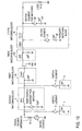
- In Fig. 5, the basic configuration of a matching circuit of the present invention is shown. The matching circuit of the present invention is constituted by a
first matching block 2 and amatching circuit part 8 consisting of lumped elements.Matching circuit part 8 is a π-type circuit constituted by asecond matching block 3, switchelements first matching block 2 is connected to a first terminal P1 to which an element 1 (a load in this example) having an impedance ZL(f) with frequency-dependent characteristics is connected. To the other end offirst matching block 2, one end ofsecond matching block 3 is connected in series. The other end ofsecond matching block 3 is connected, via a second terminal P2, to anelement 9, e.g. a signal source, with an impedance Z0 whose impedance does not depend on the frequency. Also, to the terminal on thefirst matching block 2 side ofsecond matching block 3, there is connected a series circuit ofswitch element 4 andauxiliary matching block 6. To the other end ofsecond matching block 3, there is connected a series circuit ofswitch element 5 andauxiliary matching block 7. By being connected in this way, matchingcircuit part 8 becomes a π-type circuit. - The operation of the matching circuit in Fig. 5 will be explained using Fig. 6A and Fig. 6B. Fig. 6A is a diagram showing the operation in a low frequency band f2. Fig. 6B is a diagram showing the operation in a high frequency band f1. In the case of frequency band f2, switch
elements element 1 in the frequency band f2, impedance Z1 offirst matching block 2, and impedance Z2 of second matching block 3 (below, the impedances will be omitted in portions where the same can be considered not to be particularly necessary) becomes Z0. As a result, the impedances are matched at second terminal P2. - In the frequency band f1, switch
elements circuit 8 becomes a π-type circuit in which auxiliary matching blocks 6 and 7 are respectively connected to both ends ofsecond matching block 3. Here, sincefirst matching block 2 is a matching circuit for the frequency band f1, impedance matching is obtained with impedance Z0 ofelement 9 at point A at frequency f1. Accordingly, by making a design so that, in the frequency band f1, the combined impedance Zπ seen from point A toward the second terminal P2 side becomes identical to Z0 (Z0 = Zπ), it is possible to remove the influence of the impedance ofsecond matching block 3 in the frequency band f1. Specifically, if the impedance ofauxiliary matching block 6 is taken to be Z3 and the impedance ofauxiliary matching block 7 is taken to be Z4, Z3 and Z4 may be designed so that the condition shown in Eq. 2 is met.
- As was stated above, in the frequency band f1, it is
first matching block 2 which operates to match impedance ZL(f1) ofelement 1 to impedance Z0 ofelement 9. Also, it issecond matching block 3 which operates to match the impedance ZL(f2) ofelement 1, changed by the modification of the frequency band from f1 to f2, to the impedance Z0 ofelement 9. Further, it is auxiliary matching blocks 6 and 7 which operate to remove the influence ofsecond matching block 3 which is a hindrance in frequency band f1. -
Matching circuit part 8 in Fig. 5 can also be configured with a T-type circuit. An example where the matching circuit part has been configured with a T-type circuit is shown in Fig. 7. In Fig. 7,second matching block 3 in Fig. 5 is replaced by asecond matching block 31 and a series second matchingblock 32. One end ofsecond matching block 31 is connected to point A. The other end ofsecond matching block 31 is connected to one end of series second matchingblock 32. The other end of series second matchingblock 32 is connected to second terminal P2. To the connection point ofsecond matching block 31 and series second matchingblock 32, there is connected anauxiliary matching block 34 via a switchingelement 33. - The relationship between Fig. 5 and Fig. 7 cannot be converted with the well known Y-Δ conversion (T-π conversion) relationship. In order to adopt a matching circuit equivalent to that of Fig. 5, first, the value of the impedance of
second matching block 3 must be Z2 as a condition in frequency band f2. Consequently, if the impedance ofsecond matching block 31 is taken to be Za and the impedance of series second matchingblock 32 is taken to be Zb, the relationship Z2 = Za + Zb must be satisfied. In order to choose a T-type circuit which is equivalent to a π-type circuit, the impedance value ofauxiliary matching block 34 may be designed by adding this condition. Of course, it goes without saying that matchingblock part 8 may be designed with a T-type circuit from the beginning. In this way, it is possible for matchingcircuit part 8 to have a configuration which is not limited to a π-type circuit but can also be a T-type circuit. - Fig. 8 is an example where the basic structure of this invention, shown in Fig. 5, has been generalized so that it can be adapted to a plurality of frequency bands. This matching circuit is composed of
first matching block 2, L-type blocks 43a to 43n, and shunt circuit blocks 46a to 46n. Each L-type block 43i (i = a to n) is composed of a second matching block 40i, a first switch element 41i, and a first auxiliary matching block 42i. One terminal of second matching block 40a is connected tofirst matching block 2. Also, the other end of second matching block 40a is connected to one terminal of second matching block 40b. In this way, each second matching block 40i is connected in series. First auxiliary matching block 42i is connected, via first switch element 41 i, to the terminal of second matching block 40i on the side of first terminal P1. In other words, an L-type circuit is formed by means of second matching block 40i, first switch element 41 i, and first auxiliary matching block 42i. - To the second terminal P2 side of L-
type block 43n, there are connected in parallel shunt circuit blocks 46a to 46n. Each shunt circuit block 46i (i = a to n) is composed of a second switch element 44i connected in series and a second auxiliary matching block 45i. - Below, an explanation will be given on the operation and design method of a matching circuit in which three L-
type blocks 43a to 43c and three shunt circuit blocks 46a to 46c are connected. - First, an explanation will be given for the case of frequency band f4. In the case of frequency band f4,
first switch elements 41a to 41 c andsecond switch elements 44a to 44c are all in a non-conducting state. Element 1 (impedance ZL(f4)) is connected, via three second matching blocks 40a to 40c connected in series, to element 9 (impedance Z0). Here, the impedance ZL(f) ofelement 1 changes with frequency. Also,element 9 is a signal source or the like, the impedance of which does not depend on the frequency. Here, second matching block 40c is designed so that the combined impedance ofelement 1,first matching block 2, and second matching blocks 40a and 40b is converted to Z0. If second matching block 40c is designed in this way, the impedance Z0 is matched at the second terminal P2 side end of second matching block 40c. - In the case of frequency band f3, switch element 41 c of L-type block 43c and
second switch element 44a ofshunt circuit block 46a are chosen to be in a conducting state. In this case, since first auxiliary matching block 42c and secondauxiliary matching block 45a are connected to both ends of second matching block 40c, a π-type circuit is configured. Here, second matching block 40b is designed so that the combined impedance due to element 1 (impedance ZL(f3)),first matching block 2, and second matching block 40a is matched to Z0. If second matching block 40b is designed in this way, the impedance seen from the second terminal P2 side of second matching block 40b (the first tenninal P1 side of second matching block 40c) towardelement 1 becomes Z0. Also, first auxiliary matching block 42c and secondauxiliary matching block 45a are designed so that Eq. 2 is satisfied at frequency f3. By designing in that way, the impedance seen from the first terminal P1 side of second matching block 40c (the second terminal P2 side of second matching block 40b) towardelement 9 also becomes Z0. In other words, it is possible to remove the influence of the impedance of second matching block 40c, so the impedances are matched. - In the case of frequency band f2, switch element 41b of L-type block 43b and second switch element 44b of shunt circuit block 46b are chosen to be in a conducting state. In this case, since first auxiliary matching block 42b and second auxiliary matching block 45b are connected to both ends, connected in series, of second matching block 40c and second matching block 40b, a π-type circuit is configured. Second matching block 40a is designed so that the combined impedance due to element 1 (impedance ZL(f2)) and
first matching block 2 is matched to Z0. If second matching block 40a is designed in this way, the impedance seen from the second terminal P2 side of second matching block 40a (the first terminal P1 side of second matching block 40b) towardelement 1 becomes Z0. Also, first auxiliary matching block 42b and second auxiliary matching block 45b are designed so that Eq. 2 is satisfied at frequency f2. By designing in that way, the impedance seen from the first terminal P1 side of second matching block 40b (the second terminal P2 side of second matching block 40a) towardelement 9 also becomes Z0. In other words, it is possible to remove the influence of second matching blocks 40b and 40c, so the impedances are matched. - In the case of frequency band f1,
switch element 41a of L-type block 43a and second switch element 44c of shunt circuit block 46c are in a conducting state. In this case, since firstauxiliary matching block 42a and second auxiliary matching block 45c are connected to both ends of second matching blocks 40c to 40a, a π-type circuit is configured. First matchingblock 2 is designed so that impedance ZL(f1) ofelement 1 is matched to Z0. Iffirst matching block 2 is designed in this way, the impedance seen from the second terminal P2 side of first matching block 2 (the first terminal P1 side of second matching block 40a) towardelement 1 becomes Z0. Also, firstauxiliary matching block 42a and second auxiliary matching block 45c are designed so that Eq. 2 is satisfied at frequency f1. By designing in that way, the impedance seen from the first terminal P1 side of second matching block 40a (the second terminal P2 side of first matching block 2) towardelement 9 also becomes Z0. In other words, it is possible to remove the influence of the impedances of second matching blocks 40a to 40c, so the impedances are matched. - As stated above, it is possible to combine three L-type blocks and shunt circuits to match the impedances at four frequencies. If this is generalized, the result is that it is possible, with a combination of N L-type blocks and shunt circuits, to match the impedances in N+1 frequency bands.
- Fig. 9 expresses the image of N frequency bands. The abscissa axis of Fig. 9 is the frequency and the ordinate axis is the power of transmission. In this diagram, a relation that the frequency becomes lower as N increases is shown as an example.
- Further, in Fig. 8, the frequencies are arranged in the order corresponding to shunt circuit blocks 46a to 46n. However, as long as a one-to-one relationship with first
auxiliary matching blocks 42a to 42n is satisfied, the order of arranging shunt circuit blocks 46a to 46n is indifferent. - Also, the second matching block is configured with lumped elements connected in series between the conductively connected first switch element and second switch element. Consequently, even if the number of second matching blocks becomes large, it is possible to make the whole circuit remarkably small, compared to the case of a configuration with transmission lines.
- A matching circuit generalized by using π-type circuits was explained in Fig. 8, but it is also possible to configure a generalized matching circuit using T-type circuits. In Fig. 10, there is shown an embodiment of a matching circuit using two T-type circuits. This matching circuit is composed of
first matching block 2, an L-type block part 63a, an L-type block part 63b, and asecond matching block 60c. One end offirst matching block 2 is connected to a first terminal P1 at which it is connected toelement 1. Also, the other end offirst matching block 2 is connected to one end of asecond matching block 60a inside L-type block part 63a. To the other end ofsecond matching block 60a, there is connected anauxiliary matching block 62a via afirst switch element 61a. Moreover, the other end ofsecond matching block 60a is also connected to one end of asecond matching block 60b inside L-type block part 63b. To the other end ofsecond matching block 60b, anauxiliary matching block 62b is connected via asecond switch element 61b. In addition, the other end ofsecond matching block 60b is also connected to one end ofsecond matching block 60c. Here, L-type block part 63 a is composed ofsecond matching block 60a,first switch element 61 a, andauxiliary matching block 62a. Also, L-type block part 63b is composed ofsecond matching block 60b,second switch element 61b, andauxiliary matching block 62b. Also, T-type matching circuits type block parts second matching block 60c. T-type matching circuit 64 is composed of second matching blocks 60a and 60b,first switch element 61 a, andauxiliary block 62a. Also, T-type matching circuit 65 is composed of second matching blocks 60c and 60b,second switch element 61b, andauxiliary matching block 62b. In this way, a matching circuit which matches impedances in three frequency bands is configured in two stages with T-type matching circuits - In the case of frequency band f3, switch
elements element 1 changes with the frequency band.Element 1 with an impedance ZL(f3) is connected, via the serially connected first matchingblock 2 andsecond matching blocks element 9 which has an impedance of Z0. -
Second matching block 60b andsecond matching block 60c are designed so that the combined impedance withelement 1,first matching block 2, andsecond matching block 60a becomes Z0. By designingsecond matching block 60b andsecond matching block 60c in this way, it is possible to match the impedances at second terminal P2 ofsecond matching block 60c. - In the case of frequency band f2,
switch element 61b constituting T-type matching circuit 65 is in a conducting state.Second matching block 60a is designed so that the combined impedance withelement 1, having an impedance ZL(f2), andfirst matching block 2 is taken to be Z0. By designingsecond matching block 60a in this way, the impedance seen from point D towardelement 1 becomes Z0. Also,auxiliary matching block 62b is designed so that the combined impedance of second matching blocks 60b and 60c,auxiliary matching block 62b, andelement 9 becomes Z0. Ifauxiliary matching block 62b is designed in this way, the impedance seen from point D toward theelement 9 side becomes Z0. Consequently, it is possible to match the impedances at point D. Also, even on the side of second terminal P2, the impedance seen towardelement 1 is Z0. Consequently, the combined impedance of second matching blocks 60c and 60b andauxiliary matching block 62b does not exert any influence on the matching condition. In other words,auxiliary matching block 62b removes the influence of second matching blocks 60c and 60b at frequency f2. - In the case of frequency band f1,
switch element 61b constituting T-type matching circuit 65 is in a non-conducting state, and switchelement 61a constituting T-type matching circuit 64 is in a conducting state. First matchingblock 2 is designed so that the the combined impedance with impedance ZL(f1) ofelement 1 becomes Z0. By designingfirst matching block 2 in this way, the impedance seen from point A towardelement 1 becomes Z0. Next, firstauxiliary matching block 62a is designed so that the combined impedance ofsecond matching blocks auxiliary matching block 62a, andelement 9 becomes Z0. By designing firstauxiliary matching block 62a in this way, the impedance seen from point A towardelement 9 becomes Z0. Consequently, it is possible to obtain matching of the impedances at point A. Also, on the second terminal P2 side as well, the impedance seen towardelement 1 is Z0. Consequently, the combined impedance ofsecond matching blocks auxiliary matching block 62a does not exert influence any more on the matching conditions. In other words,auxiliary matching block 62a removes the influence ofsecond matching blocks - With the aforementioned explanation, the case where
switch element 61b is non-conducting was explained. However, it is not mandatory to takeswitch element 61 b to be non-conducting. Incase switch element 61 b is taken to be conducting when the frequency band is f1,auxiliary matching block 62a may be designed with that assumption. - In this way, it is possible to configure a matching circuit handling three frequency bands by means of two T-
type matching circuits - An example showing a generalization of the T-type matching circuit explained in
Embodiment 3 is shown in Fig. 11. The configuration up to the second-stage L-type block 63b seen fromfirst matching block 2 is identical to that of Fig. 10. On the second terminal P2 side of second-stage L-type block 63b, L-type blocks are added. In Fig. 11, a total ofN L-type blocks 63a to 63n are connected. To the other end of L-type block 63n, one end of series second matchingblock 70 is connected, the other end of series second matchingblock 70 being connected to second terminal P2. N is an integer equal to or greater than 1. The matching circuit shown in Fig. 11 is a subordinate connection configuration ofN T-type matching circuits and is capable of matching in N+1 frequency bands. The operation is the same as in Fig. 10. - Another T-type matching circuit embodiment is shown in Fig. 12. In Fig. 10, a T-type circuit was formed using second matching blocks of adjacent L-type blocks. Fig. 12 is an example in which a plurality of auxiliary matching blocks are connected, via switch elements, between two second matching blocks connected in series. This matching circuit is composed of
first matching block 2 and T-type matching circuits type matching circuit 83a is composed of second matching blocks 80a and 80b, aswitch element 81a, and anauxiliary matching block 82a. One end ofsecond matching block 80a is connected tofirst matching block 2. The other end ofsecond matching block 80a is connected to one end ofsecond matching block 80b. Also,auxiliary matching block 82a is connected, viaswitch element 81a, betweensecond matching block 80a andsecond matching block 80b. By this kind of connection relationship, second matching blocks 80a and 80b,switch element 81 a, andauxiliary matching block 82a make up a T-type circuit. T-type matching circuit 83b is composed of second matching blocks 80c and 80d, aswitching element 81b, and anauxiliary matching block 82b. T-type matching circuit 83c is composed of second matching blocks 80c and 80d, asecond switching element 84, and anauxiliary matching block 85. Here, second matching blocks 80c and 80d are constituent parts of both T-type matching circuit 83b and T-type matching circuit 83c. With this configuration,auxiliary matching block 82b is connected, viaswitch element 81b, to the connection point ofsecond matching block 80c andsecond matching block 80d. Moreover,auxiliary matching block 85 is also connected, viasecond switch element 84, to the connection point ofsecond matching block 80c andsecond matching block 80d. One end ofsecond matching block 80c is connected tosecond matching block 80b. Also, the other end ofsecond matching block 80d is connected to the second terminal P2 to whichelement 9 is connected. - As stated above, a T-type matching circuit may be connected in multiple stages between
element 1 andelement 9. The present embodiment is capable of matching in three frequency bands by means of three T-type matching circuits. - In the case of frequency band f3, switch
elements second switch element 84 are non-conducting. Second matching blocks 80c and 80d are designed so that the combined impedance with element 1 (impedance ZL(f3)),first matching block 2, andsecond matching blocks element 9 in the frequency band f3. Consequently, impedance matching can be obtained at second terminal P2. - In the case of frequency band f2, it is
only switch element 81 b forming T-type matching circuit 83b that is conducting. Second matching blocks 80a and 80b are designed so that the combined impedance of element 1 (impedance ZL(f2)) andfirst matching block 2 is made to match the impedance Z0 ofelement 9 in the frequency band f2. Consequently, the impedance seen from the second terminal P2 side ofsecond matching block 80b (the first terminal P1 side ofsecond matching block 80c) towardelement 1 becomes Z0. Also,auxiliary matching block 82b is designed so that the combined impedance of second matching blocks 80c and 80d,auxiliary matching block 82b, andelement 9 becomes Z0 at the frequency f2. By designingauxiliary matching block 82b in this way, the impedance seen from the first terminal P1 side ofsecond matching block 80c (the second terminal P2 side ofsecond matching block 80b) towardelement 9 becomes Z0 at the frequency f2. Consequently, the impedances are matched. - In the case of frequency band f1,
switch element 81a andsecond switch element 84 are conducting. First matchingblock 2 is designed so that the impedance of element 1 (impedance ZL(f2)) is made to match the impedance Z0 ofelement 9 in the frequency band f1. Consequently, the impedance seen from the second terminal P2 side offirst matching block 2 towardelement 1 becomes Z0.Auxiliary matching block second matching blocks auxiliary matching block 82a, andelement 9 becomes Z0. Consequently, the impedance seen from the second terminal P2 side of first matching block 2 (the first terminal P1 side ofsecond matching block 80a) towardelement 9 becomes Z0. - In this way, in the case of connecting T-type matching circuits, the two second matching blocks and the auxiliary matching block only make up a set with respect to one frequency band. In order to make the second matching blocks handle a plurality of frequency bands, a plurality of auxiliary matching blocks becomes necessary.
- As explained in
Embodiment 5, in the case of connecting T-type matching circuits, there are cases in which, for two second matching blocks, a plurality of auxiliary matching blocks becomes necessary. In Fig. 13, there is shown a configuration example of a matching circuit using an additional auxiliary matching block. Fig. 13 shows a configuration example where asecond switch element 90 and a secondauxiliary matching block 91 have been connected in series withauxiliary matching block 82b of Fig. 12. Having auxiliary matching blocks connected in series in two stages is done so that second matching blocks 80c and 80d constituting T-type matching circuit 83b can handle two frequency bands. - In the case of this example, in order for the circuit to function also in the case where
only switch 81b is conducting, it is necessary to chooseauxiliary matching block 82b to be a transmission line. In case it is not desired to provide such conditions,switch element 81b may be configured with a Single Pole Double Throw (SPDT) switch or a multi-contact switch, and switching may be performed between auxiliary matching blocks with different values. - If the circuit configuration is such that the impedance of the second matching block inserted between
element 1 andelement 9 can be made Z0, seen from both the aforementioned matching point and theelement 9 directions, the invention is not limited to the T type or the π type. - In the explanations so far, the second matching blocks were explained as black boxes. In Fig. 14, there is shown a configuration example of
second matching block 3 of Fig. 5.Second matching block 3 is constituted by an L-type circuit consisting of aseries matching block 100, aswitch element 101 for matching, and amatching element 102. One end ofseries matching block 100 is connected tofirst matching block 2.Matching element 102 is connected to the other end ofseries matching block 100 viaswitch element 101 for matching. - In the case of frequency band f1, switch
elements element 101 for matching is conducting. At this point, the sum of the impedances ofelement 1 andfirst matching block 2 are matched to impedance Z0 ofelement 9 by means ofseries matching block 100 and matchingelement 102. - In the case of frequency band f2, switch
elements switch element 101 for matching is chosen to be non-conducting. As for this configuration, it is possible, by the existence of matchingelement 102, to broaden the options ofsecond matching block 3 andauxiliary matching block second matching block 3 by configuringsecond matching block 3 withseries matching block 100,first switch element 101 for matching, and matchingelement 102. In general, the values of the lumped elements constitutingsecond matching block 3 are discrete, making delicate tuning difficult. However, according to this embodiment, it is possible to broaden the lumped element options. - Another configuration of the second matching block is shown in Fig. 15.
Second matching block 3 in Fig. 15 is constituted by a T-type circuit consisting of second matching blocks 60a and 60b, aswitch element 110 for matching, and amatching element 111.Second matching block 60a andsecond matching block 60b are connected in series. One end ofsecond matching block 60a is connected tofirst matching block 2. The other end ofsecond matching block 60b is connected to second terminal P2.Matching element 111 is connected, viaswitch element 110 for matching, to the connection point ofsecond matching block 60a andsecond matching block 60b. -
Switch element 110 for matching and matchingelement 111 are provided in order to increase the freedom in designing the second matching blocks andauxiliary matching block 7 andauxiliary matching block 6. Regarding the function, it is the same as inEmbodiment 7. - Another configuration of the second matching blocks is shown in Fig. 16. Fig. 16 differs from Fig. 7 in the point that, on the second terminal P2 side of T-type
matching circuit part 30, there are provided aswitch element 120 form matching and amatching element 121. In the case of frequency f2,switch element 33 andswitch element 120 for matching are e.g. made to conduct exclusively.Matching element 121 andsecond matching block element 1 andfirst matching block 2 is chosen to be Z0. By configuring the circuit in this way, it is possible to increase the freedom in designing the second matching blocks. - In the same way as configuring
second matching block 3 by using a plurality of elements,first matching block 2 may also be configured with a plurality of elements. A configuration example thereof is shown in Fig. 17. In this example,first matching block 2 is composed of a firstseries matching block 130 and anauxiliary matching block 131 connected to one end thereof. Further,auxiliary matching block 131 may be connected to either end of firstseries matching block 130. Firstseries matching block 130 is connected toelement 9 via matchingcircuit part 8. - As for the configuration of the first matching block, modes other than this are possible. All things considered, in a predetermined frequency band f, if the impedance seen from point A toward element 1 (impedance ZL(f)) can be chosen to be Z0, any circuit configuration is acceptable.
- An exemplification of the matching circuit which has been gradually explained this far is shown in Fig. 18. Fig. 18 is an example applied to an amplifying circuit operating in two frequency bands, the 2 GHz band and the 1 GHz band. On the input side of an
FET 140, which is a power amplifier element, the matching circuit shown in Fig. 17 is connected, and on the input side, the matching circuit shown in Fig. 16 is connected. As for the matching circuit on the input side,first matching block 2 has become afirst matching block 141. The output side matching circuit has, based on the matching circuit shown in Fig. 16,first matching block 2 configured with afirst matching block 142. - The operation has been explained this far, so an explanation thereof will be omitted. In Fig. 19A and Fig. 19B, the simulation results for the amplifier in Fig. 18 are shown. Fig. 19A is a diagram showing the frequency characteristics in the case where the circuit has been set for the 2 GHz band. The abscissa axis indicates the frequency and the ordinate axis indicates the S parameter. The reflection S11 of the signal input into first terminal P1 gets attenuated abruptly at 2 GHz. The transmission S21 of the signal input in first terminal P1 exhibits a value of approximately 14 dB at 2 GHz, so the circuit transmits well. Fig. 19B is a diagram showing the frequency characteristics in the case where the circuit has been set for the 1 GHz band. The reflection S11 of the signal input into first terminal P1 gets attenuated abruptly at 1 GHz. The transmission S21 of the signal input in first terminal P1 exhibits a value of approximately 19 dB at 1 GHz, so the circuit transmits well. It is seen that the matching circuit according to the present invention functions as a multiband matching circuit.
- The matching circuit according to the present invention has an impedance seen from both ends of a second matching block, inserted between
element 9 andelement 1 and formed with lumped-parameter elements, which is made to match the impedance Z0 by means of an auxiliary matching block. Also, by raising the number of auxiliary matching blocks, a matching circuit handling a plurality of frequency bands is adopted. Further, since the second matching block is formed with lumped elements, it can be made smaller than prior-art matching circuits configured with transmission lines. - The effect of the reduction in size is possible to see by comparing Fig. 3 showing a conventional matching circuit and Fig. 5 showing the matching circuit of the present invention. Fig. 3 and Fig. 5 are diagrams of circuits made capable of matching in two frequency bands together. As against the conventional matching circuit (Fig. 3), the matching circuit of the present invention (Fig. 5) requires in total two additional components, one switch element and one auxiliary matching circuit. However, the
delay circuit 172 required in the conventional matching circuit is a large-size component. The size thereof varies with the frequency band and the used power amplification element, but when e.g., the frequency band is taken to be 1 GHz with a certain amplification element, the width is 0.63 mm and the length is 9.22 mm, or the length is 15.32 mm. - On the other hand, the matching circuit of the present invention can be configured with a chip circuit commonly known by the name 0603 and having a width of 0.3 mm and a length of 0.6 mm and a Monolithic Microwave Integrated Circuit several mm square. In other words, all of the components constituting the matching circuit of the present invention end up amply fitting into the space of
delay circuit 172. In order to handle still more frequency bands, the number ofdelay circuits 172 must be increased. Consequently, as a matching circuit for multiband use, the matching circuit of the present invention can be further reduced in size, compared to a conventional matching circuit.
Claims (7)
- A matching circuit making the impedance at predetermined plural frequencies match with an element whose impedance has frequency-dependent characteristics, comprising:a first matching block connected at one end to a first terminal to which said element whose impedance has frequency-dependent characteristics is connected;one or more second matching blocks consisting of lumped elements and connected in series to said first matching block;one or more switch elements; andone or more auxiliary matching blocks connected to said second matching block(s) via said switch element(s).
- The matching circuit according to Claim 1, comprising:N L-type circuits each consisting of one said second matching block and a series circuit of one first said switch element (below referred to as the "first switch element"), connected to one end of said second matching block, and one first said auxiliary matching block (below referred to as the "first auxiliary matching block"); andN shunt circuit block parts, each consisting of a series circuit of one second said switch element (below referred to as the "second switch element") and one second said auxiliary matching block (below referred to as the "second auxiliary matching block"); andwhereinN is an integer equal to or greater than 1,said N L-type circuits have one end of the second matching block of the first L-type circuit connected in series to said first matching block and one end of the second matching block of the next-stage L-type circuit connected to the other end of said second matching block,N said shunt circuit block parts are connected to the other end of the second matching block of the last-stage L-type circuit, anda π-type circuit is formed by a second auxiliary matching block connected to one said second switch element made to conduct, a first auxiliary matching block connected to one said first switch element made to conduct, and the second matching blocks between these.
- The matching circuit according to Claim 1, comprising
N L-type circuits each consisting of said second matching block and a series circuit of said switch element, connected to one end of said second matching block, and said auxiliary matching block; and a series second matching block;
wherein
N being an integer equal to or greater than 1,
said N L-type circuits have one end of the second matching block of the first L-type circuit connected in series to said first matching block and one end of the second matching block of the next-stage L-type circuit connected to the other end of said second matching block,
one end of said second matching block is connected to the other end of the second matching block of the last-stage L-type circuit;
the other end of said second matching block is connected to an element whose characteristics do not depend on the frequency, and
a T-type circuit is constituted by one said series circuit, said switch element of which is taken to be in a conducting state, and the second matching blocks on both sides thereof., - The matching circuit according to Claim 2 or 3, wherein N equals 1.
- The matching circuit according to any of Claims 1 to 4,
wherein said second matching block is constituted by an L-type circuit consisting of a series matching block and a series circuit of a switch element, connected to said series matching block, and a matching element. - A matching circuit, comprising:a first matching block connected at one end to a first terminal to which an element whose impedance has frequency-dependent characteristics is connected; anda matching circuit part constituting a π-type circuit by a second matching block connected in series to said first matching block, and switch element and auxiliary matching block series circuits respectively connected to both ends of said second matching block; andwherein said second matching block is constituted by lumped elements.
- A matching circuit, comprising:a first matching block connected at one end to a first terminal to which an element whose impedance has frequency-dependent characteristics is connected; anda matching circuit part constituting a T-type circuit by a second matching block connected at one end to said first matching block, the next second matching block connected at one end to the other end of said second matching block, a series circuit of a switch element, connected between said second matching block and the next second matching block, and an auxiliary matching block; andwherein said second matching block and said series second matching block are constituted by lumped elements.
Applications Claiming Priority (1)
| Application Number | Priority Date | Filing Date | Title |
|---|---|---|---|
| JP2005148621A JP4838536B2 (en) | 2005-05-20 | 2005-05-20 | Matching circuit |
Publications (2)
| Publication Number | Publication Date |
|---|---|
| EP1724936A2 true EP1724936A2 (en) | 2006-11-22 |
| EP1724936A3 EP1724936A3 (en) | 2007-03-21 |
Family
ID=36609465
Family Applications (1)
| Application Number | Title | Priority Date | Filing Date |
|---|---|---|---|
| EP06010268A Withdrawn EP1724936A3 (en) | 2005-05-20 | 2006-05-18 | Matching circuit |
Country Status (5)
| Country | Link |
|---|---|
| US (3) | US20060261911A1 (en) |
| EP (1) | EP1724936A3 (en) |
| JP (1) | JP4838536B2 (en) |
| KR (1) | KR100748040B1 (en) |
| CN (1) | CN100527611C (en) |
Cited By (1)
| Publication number | Priority date | Publication date | Assignee | Title |
|---|---|---|---|---|
| EP1936814A1 (en) | 2006-12-20 | 2008-06-25 | NTT DoCoMo, Inc. | Matching circuit and dual-band power amplifier |
Families Citing this family (20)
| Publication number | Priority date | Publication date | Assignee | Title |
|---|---|---|---|---|
| JP4838572B2 (en) | 2005-11-24 | 2011-12-14 | 株式会社エヌ・ティ・ティ・ドコモ | Stabilization circuit, multiband amplifier circuit |
| JP2007329641A (en) * | 2006-06-07 | 2007-12-20 | Mitsubishi Electric Corp | Frequency / bandwidth switching amplifier |
| CN101212230B (en) * | 2006-12-26 | 2012-07-11 | 中兴通讯股份有限公司 | Device and method for implementing DVB-H antenna matching network for mobile telephone |
| JP4308882B2 (en) | 2007-04-09 | 2009-08-05 | パナソニック株式会社 | Dual frequency matching circuit and portable terminal comprising the same |
| CN101558561A (en) | 2007-04-09 | 2009-10-14 | 松下电器产业株式会社 | Two frequency matching circuit |
| JP5079387B2 (en) * | 2007-05-10 | 2012-11-21 | 株式会社エヌ・ティ・ティ・ドコモ | Matching circuit |
| JP4956312B2 (en) * | 2007-07-20 | 2012-06-20 | 株式会社アドバンテスト | Delay line |
| WO2009028200A1 (en) | 2007-08-29 | 2009-03-05 | Panasonic Corporation | Double channel matching circuit |
| JP4308890B2 (en) | 2007-08-29 | 2009-08-05 | パナソニック株式会社 | Dual frequency matching circuit and portable terminal comprising the same |
| CN101465679B (en) * | 2007-12-20 | 2012-09-05 | 启碁科技股份有限公司 | Wireless signal transceiving device and related devices |
| JP2010087934A (en) * | 2008-09-30 | 2010-04-15 | Panasonic Corp | Matching circuit, high-frequency power amplifier and cellular phone |
| JP5453120B2 (en) * | 2009-01-30 | 2014-03-26 | 株式会社Nttドコモ | Multiband matching circuit and multiband power amplifier |
| JP5102825B2 (en) * | 2009-01-30 | 2012-12-19 | 株式会社エヌ・ティ・ティ・ドコモ | Multiband matching circuit and multiband power amplifier |
| JP5788964B2 (en) * | 2010-03-26 | 2015-10-07 | ドイッチェ テレコム アーゲー | Device for decoupling radio frequency signals transmitted on a data transmission line |
| US8712348B2 (en) * | 2010-09-01 | 2014-04-29 | Samsung Electronics Co., Ltd. | Apparatus and method for controlling a tunable matching network in a wireless network |
| JP5656653B2 (en) | 2011-01-07 | 2015-01-21 | 株式会社Nttドコモ | Variable matching circuit |
| WO2012104972A1 (en) * | 2011-01-31 | 2012-08-09 | 富士通株式会社 | Matching device, transmission amplifier and wireless communication device |
| US8975981B2 (en) * | 2011-09-13 | 2015-03-10 | Qualcomm Incorporated | Impedance matching circuits with multiple configurations |
| JP6597461B2 (en) * | 2015-07-02 | 2019-10-30 | 株式会社村田製作所 | Amplifier circuit |
| CN109659693B (en) * | 2018-12-12 | 2021-08-24 | 维沃移动通信有限公司 | An antenna structure and communication terminal |
Family Cites Families (4)
| Publication number | Priority date | Publication date | Assignee | Title |
|---|---|---|---|---|
| JPH06232657A (en) * | 1993-02-03 | 1994-08-19 | N T T Idou Tsuushinmou Kk | High frequency amplifier |
| JPH1056305A (en) | 1996-08-09 | 1998-02-24 | Mitsubishi Electric Corp | Impedance matching circuit and thin film probe for measurement |
| KR20030070198A (en) * | 2002-02-21 | 2003-08-29 | 엘지전자 주식회사 | Multi-band matching circuit |
| WO2004082138A1 (en) * | 2003-03-14 | 2004-09-23 | Ntt Docomo Inc. | Matching circuit |
-
2005
- 2005-05-20 JP JP2005148621A patent/JP4838536B2/en not_active Expired - Fee Related
-
2006
- 2006-05-17 US US11/434,889 patent/US20060261911A1/en not_active Abandoned
- 2006-05-18 EP EP06010268A patent/EP1724936A3/en not_active Withdrawn
- 2006-05-18 KR KR1020060044565A patent/KR100748040B1/en not_active Expired - Fee Related
- 2006-05-22 CN CNB2006100850637A patent/CN100527611C/en not_active Expired - Fee Related
-
2009
- 2009-03-03 US US12/396,980 patent/US7750756B2/en not_active Expired - Fee Related
- 2009-03-17 US US12/405,891 patent/US7750757B2/en not_active Expired - Fee Related
Cited By (2)
| Publication number | Priority date | Publication date | Assignee | Title |
|---|---|---|---|---|
| EP1936814A1 (en) | 2006-12-20 | 2008-06-25 | NTT DoCoMo, Inc. | Matching circuit and dual-band power amplifier |
| US7710217B2 (en) | 2006-12-20 | 2010-05-04 | Ntt Docomo, Inc. | Matching circuit and dual-band power amplifier |
Also Published As
| Publication number | Publication date |
|---|---|
| US20090167458A1 (en) | 2009-07-02 |
| US7750756B2 (en) | 2010-07-06 |
| US20090179711A1 (en) | 2009-07-16 |
| KR20060120449A (en) | 2006-11-27 |
| EP1724936A3 (en) | 2007-03-21 |
| CN100527611C (en) | 2009-08-12 |
| US20060261911A1 (en) | 2006-11-23 |
| CN1866735A (en) | 2006-11-22 |
| JP2006325153A (en) | 2006-11-30 |
| KR100748040B1 (en) | 2007-08-09 |
| US7750757B2 (en) | 2010-07-06 |
| JP4838536B2 (en) | 2011-12-14 |
Similar Documents
| Publication | Publication Date | Title |
|---|---|---|
| US7750757B2 (en) | Matching circuit | |
| CN110048735B (en) | System and method for radio frequency filter | |
| US8487713B2 (en) | Multiband matching circuit and multiband power amplifier | |
| JP4464919B2 (en) | Matching circuit | |
| US7710217B2 (en) | Matching circuit and dual-band power amplifier | |
| EP2214311B1 (en) | Multiband matching circuit and multiband power amplifier | |
| US7656228B2 (en) | Matching circuit and multi-band amplifier | |
| EP1450486A1 (en) | Multi-Mode Filter | |
| CN108233952B (en) | Communication module | |
| WO2008014029A2 (en) | Re-configurable impedance matching and harmonic filter system | |
| EP2421151A2 (en) | Multiband impedance matching circuit | |
| US11838003B2 (en) | Composite filter device | |
| JP4744615B2 (en) | Microwave and millimeter wave band amplifier circuit and millimeter wave radio using the same | |
| JPWO2005048448A1 (en) | High frequency amplifier | |
| KR20140025208A (en) | Wilkinson power divider/combiner having a stub members | |
| EP1791253A2 (en) | Stabilization circuit and multiband amplification circuit | |
| US7944330B2 (en) | Resonant element and high frequency filter, and wireless communication apparatus equipped with the resonant element or the high frequency filter | |
| CN116632488B (en) | Differential power divider, transmitting link system and receiving link system | |
| EP2178219B1 (en) | A method for broadband matching and a network element thereof | |
| KR101589587B1 (en) | T-type dual band impedance matching circuit and the design method thereof | |
| CN114531167A (en) | High-frequency signal transceiving circuit | |
| EP4544675A1 (en) | Dual-band dual-output ports power amplifier arrangements | |
| WO2024057696A1 (en) | High frequency circuit and communication apparatus | |
| EP3160046B1 (en) | Matching network circuit, and associated apparatus with shared matching network circuit |
Legal Events
| Date | Code | Title | Description |
|---|---|---|---|
| PUAI | Public reference made under article 153(3) epc to a published international application that has entered the european phase |
Free format text: ORIGINAL CODE: 0009012 |
|
| 17P | Request for examination filed |
Effective date: 20060518 |
|
| AK | Designated contracting states |
Kind code of ref document: A2 Designated state(s): AT BE BG CH CY CZ DE DK EE ES FI FR GB GR HU IE IS IT LI LT LU LV MC NL PL PT RO SE SI SK TR |
|
| AX | Request for extension of the european patent |
Extension state: AL BA HR MK YU |
|
| PUAL | Search report despatched |
Free format text: ORIGINAL CODE: 0009013 |
|
| AK | Designated contracting states |
Kind code of ref document: A3 Designated state(s): AT BE BG CH CY CZ DE DK EE ES FI FR GB GR HU IE IS IT LI LT LU LV MC NL PL PT RO SE SI SK TR |
|
| AX | Request for extension of the european patent |
Extension state: AL BA HR MK YU |
|
| AKX | Designation fees paid |
Designated state(s): DE GB |
|
| 17Q | First examination report despatched |
Effective date: 20071213 |
|
| STAA | Information on the status of an ep patent application or granted ep patent |
Free format text: STATUS: THE APPLICATION IS DEEMED TO BE WITHDRAWN |
|
| 18D | Application deemed to be withdrawn |
Effective date: 20120908 |