EP1723402B1 - Verification de l'etancheite des connexions de plaquettes par metallisation, et structure de verification servant a la mise en oeuvre de ce procede - Google Patents
Verification de l'etancheite des connexions de plaquettes par metallisation, et structure de verification servant a la mise en oeuvre de ce procede Download PDFInfo
- Publication number
- EP1723402B1 EP1723402B1 EP05729617A EP05729617A EP1723402B1 EP 1723402 B1 EP1723402 B1 EP 1723402B1 EP 05729617 A EP05729617 A EP 05729617A EP 05729617 A EP05729617 A EP 05729617A EP 1723402 B1 EP1723402 B1 EP 1723402B1
- Authority
- EP
- European Patent Office
- Prior art keywords
- cavity
- test
- melt
- disc
- microelectromechanical
- Prior art date
- Legal status (The legal status is an assumption and is not a legal conclusion. Google has not performed a legal analysis and makes no representation as to the accuracy of the status listed.)
- Expired - Lifetime
Links
- 238000012360 testing method Methods 0.000 title claims abstract description 108
- 238000000034 method Methods 0.000 title claims abstract description 53
- 229910052751 metal Inorganic materials 0.000 claims abstract description 8
- 239000002184 metal Substances 0.000 claims abstract description 8
- 238000002844 melting Methods 0.000 claims description 34
- 230000008018 melting Effects 0.000 claims description 33
- 239000000155 melt Substances 0.000 claims description 31
- 238000012544 monitoring process Methods 0.000 claims description 17
- 239000004020 conductor Substances 0.000 claims description 5
- 229910052782 aluminium Inorganic materials 0.000 claims description 4
- XAGFODPZIPBFFR-UHFFFAOYSA-N aluminium Chemical compound [Al] XAGFODPZIPBFFR-UHFFFAOYSA-N 0.000 claims description 4
- 238000013461 design Methods 0.000 claims description 3
- 238000010309 melting process Methods 0.000 claims description 3
- 238000000275 quality assurance Methods 0.000 claims description 2
- 239000004411 aluminium Substances 0.000 claims 1
- 235000012431 wafers Nutrition 0.000 abstract description 9
- 238000004519 manufacturing process Methods 0.000 description 25
- 230000000875 corresponding effect Effects 0.000 description 12
- 230000035882 stress Effects 0.000 description 11
- 238000005259 measurement Methods 0.000 description 8
- 210000003298 dental enamel Anatomy 0.000 description 6
- 239000004065 semiconductor Substances 0.000 description 4
- 238000003908 quality control method Methods 0.000 description 3
- 229910052710 silicon Inorganic materials 0.000 description 3
- 239000010703 silicon Substances 0.000 description 3
- 238000005033 Fourier transform infrared spectroscopy Methods 0.000 description 2
- XUIMIQQOPSSXEZ-UHFFFAOYSA-N Silicon Chemical compound [Si] XUIMIQQOPSSXEZ-UHFFFAOYSA-N 0.000 description 2
- 239000002131 composite material Substances 0.000 description 2
- 238000010276 construction Methods 0.000 description 2
- 230000000694 effects Effects 0.000 description 2
- 238000005516 engineering process Methods 0.000 description 2
- 238000011156 evaluation Methods 0.000 description 2
- 239000011521 glass Substances 0.000 description 2
- 238000004971 IR microspectroscopy Methods 0.000 description 1
- 230000032683 aging Effects 0.000 description 1
- 150000001875 compounds Chemical class 0.000 description 1
- 230000002950 deficient Effects 0.000 description 1
- 230000001419 dependent effect Effects 0.000 description 1
- 238000011161 development Methods 0.000 description 1
- 230000018109 developmental process Effects 0.000 description 1
- 238000009826 distribution Methods 0.000 description 1
- 238000004100 electronic packaging Methods 0.000 description 1
- 230000007613 environmental effect Effects 0.000 description 1
- 230000008020 evaporation Effects 0.000 description 1
- 238000001704 evaporation Methods 0.000 description 1
- 238000011835 investigation Methods 0.000 description 1
- 239000007788 liquid Substances 0.000 description 1
- 230000007774 longterm Effects 0.000 description 1
- 239000000463 material Substances 0.000 description 1
- 239000012528 membrane Substances 0.000 description 1
- 238000001465 metallisation Methods 0.000 description 1
- 238000002360 preparation method Methods 0.000 description 1
- 238000012372 quality testing Methods 0.000 description 1
- 150000003376 silicon Chemical class 0.000 description 1
- 238000004611 spectroscopical analysis Methods 0.000 description 1
Images

Classifications
-
- G—PHYSICS
- G01—MEASURING; TESTING
- G01M—TESTING STATIC OR DYNAMIC BALANCE OF MACHINES OR STRUCTURES; TESTING OF STRUCTURES OR APPARATUS, NOT OTHERWISE PROVIDED FOR
- G01M3/00—Investigating fluid-tightness of structures
- G01M3/02—Investigating fluid-tightness of structures by using fluid or vacuum
- G01M3/26—Investigating fluid-tightness of structures by using fluid or vacuum by measuring rate of loss or gain of fluid, e.g. by pressure-responsive devices, by flow detectors
- G01M3/28—Investigating fluid-tightness of structures by using fluid or vacuum by measuring rate of loss or gain of fluid, e.g. by pressure-responsive devices, by flow detectors for pipes, cables or tubes; for pipe joints or seals; for valves ; for welds
-
- B—PERFORMING OPERATIONS; TRANSPORTING
- B81—MICROSTRUCTURAL TECHNOLOGY
- B81C—PROCESSES OR APPARATUS SPECIALLY ADAPTED FOR THE MANUFACTURE OR TREATMENT OF MICROSTRUCTURAL DEVICES OR SYSTEMS
- B81C99/00—Subject matter not provided for in other groups of this subclass
- B81C99/0035—Testing
- B81C99/004—Testing during manufacturing
-
- G—PHYSICS
- G01—MEASURING; TESTING
- G01M—TESTING STATIC OR DYNAMIC BALANCE OF MACHINES OR STRUCTURES; TESTING OF STRUCTURES OR APPARATUS, NOT OTHERWISE PROVIDED FOR
- G01M3/00—Investigating fluid-tightness of structures
- G01M3/02—Investigating fluid-tightness of structures by using fluid or vacuum
- G01M3/26—Investigating fluid-tightness of structures by using fluid or vacuum by measuring rate of loss or gain of fluid, e.g. by pressure-responsive devices, by flow detectors
- G01M3/28—Investigating fluid-tightness of structures by using fluid or vacuum by measuring rate of loss or gain of fluid, e.g. by pressure-responsive devices, by flow detectors for pipes, cables or tubes; for pipe joints or seals; for valves ; for welds
- G01M3/2853—Investigating fluid-tightness of structures by using fluid or vacuum by measuring rate of loss or gain of fluid, e.g. by pressure-responsive devices, by flow detectors for pipes, cables or tubes; for pipe joints or seals; for valves ; for welds for pipe joints or seals
- G01M3/2869—Investigating fluid-tightness of structures by using fluid or vacuum by measuring rate of loss or gain of fluid, e.g. by pressure-responsive devices, by flow detectors for pipes, cables or tubes; for pipe joints or seals; for valves ; for welds for pipe joints or seals for seals not incorporated in a pipe joint
Definitions
- the invention relates to a method and an arrangement for quality control, ie a leak test of disc bonds as they are used for example for the production of MEMS (microelectromechanical structures) by, for example, glass and silicon wafers are formed to produce hermetically sealed cavities or cavities in which the micromechanical sensor part is located.
- MEMS microelectromechanical structures
- Such sensor parts require a high density of the cavity, since the reliability and life of the device is highly dependent on the tightness of the disc connection.
- the procedure is such that in the preparation of the bonding process using special control methods, eg. B. by infrared microscopy, the tightness is tested and depending on the process parameters are optimized. Leakage, which can arise in the current production, show up much later by data change of the finished components. The sorting out of the finished components, however, is a relatively expensive process, since then a large part of very complex and complex process steps for components that do not meet the required specifications, was then spend.
- special control methods eg. B. by infrared microscopy
- DE-B 197 39 961 describes a method for determining the gas pressure in a cavity with deformable walls of a semiconductor device, which is based on a resonance frequency measurement. Furthermore, it is off DE-A 101 36 219 a method is known in which for the tightness test of hermetically sealed sensors, a capacitance measurement under defined conditions in a test liquid immersed specimens is made, in which case the specimens were previously exposed to a vacuum.
- the object is achieved according to a first aspect of the present invention by a method for evaluating the tightness of disk connections, the method comprising producing a test structure.
- the test structure is formed by forming a micromechanical sensor structure and an adjacent fused structure having electrical interconnects and first contact pads connected to the micromechanical sensor structure and second contact pads connected to the fused structure on a base disk, and a cavity is formed by bonding a cover disk with the base disk is created such that the micromechanical sensor structure and the melt structure lie in the cavity.
- the method comprises impressing a current into the second contacting islands in order to melt the enamel structure for the purpose of tightness testing of the cavity, thereby producing a pressure change in the interior of the cavity, which is measured over time with the aid of the micromechanical sensor structure.
- the method further comprises producing a plurality of microelectromechanical structures (MEMS) on the wafer connection.
- MEMS microelectromechanical structures
- the tightness or reliability of the MEMS during the production process can thus be determined very precisely, since the process parameters relating to the process of producing the test structure essentially affect the production of the MEMS structures in an identical manner.
- a plurality of test structures are produced at specific locations of the wafer connection.
- test structure under the changed pressure is exposed to stress conditions in a targeted manner, wherein statements about the reliability are obtained by comparing the measured values of the micromechanical sensor structure before and after the stress condition has been applied.
- the predefined stress may include operation at certain temperature conditions, such as at elevated or low temperatures, and / or operation at certain humidity conditions, and / or operation at certain mechanical loads, and the like.
- the operation at elevated temperatures and the behavior of the test structure recognized from this operation with regard to the change in tightness it is possible to infer the expected aging of the test structure or other components.
- the plurality of test structures are arranged according to predetermined quality control criteria for the microelectromechanical structures.
- a method of monitoring a microelectromechanical structure comprises producing a test structure according to a manufacturing method as described in the preceding embodiments. Further, the method includes forming the microelectromechanical structure to form a functional dressing with the test structure. Furthermore, the microelectromechanical structure is operated and a current is impressed into the enamel structure of the test structure. Finally, the readings of the micro-mechanical sensor structure evaluated to perform an online monitoring of the microelectromechanical structure.
- test structure and the MEMS as a dressing, even after the components have been singulated, the function of the MEMS can also be monitored during the phase of the application.
- the melt structure of the test structure has a plurality of desired melting points
- the method further comprising: triggering a melting operation of the plurality of desired melting points in succession and evaluating the measurement results obtained by the micromechanical sensor structure to perform the online monitoring.
- test structure can also be used during the production phase of the association for the determination of measurement data.
- test structure for testing the tightness of disc bonds.
- the test structure comprises a region of a base disk, a region of a cover disk and a cavity which is formed by disk connection of the base disk and the cover disk.
- the test structure comprises a pressure-sensitive micromechanical structure, which is arranged in the cavity (5), and a melt structure, which is arranged in the cavity.
- the test structure further includes first contacting islands that lie outside of the cavity and are connected to the pressure-sensitive micromechanical structure, and second contacting islands, which are arranged outside the cavity and are connected to the melt structure.
- interconnects are provided which form a connection from the enamel structure to the second contacting islands and from the pressure-sensitive micromechanical structure to the first contacting islands.
- the melt structure has a desired melting point. This allows defined states to be achieved during melting and evaporation of the material of the desired melting point.
- a plurality of melting points are provided in the melt structure, wherein the melting points are defined by the design of the structure, whereby the melting process in a limited number can be repeated in succession.
- the provision of a plurality of desired melting points enables efficient online monitoring of the test structure and thus possibly also in association with other MEMS structures present, since tightness tests can be carried out during different operating phases of the test structure or associated MEMS structures. Furthermore, it is possible to examine the test structure several times under different stress conditions, so that a very detailed test can be carried out in a local manner on the same chip surface.
- the molten metal structure is constructed of metal and in the case of current flow melting parts in the inner region run meander-shaped.
- the metal of the enamel structure comprises aluminum.
- a disk connection comprising a microelectromechanical structure (MEMS) and a test structure for evaluating the tightness of the disk connection, constructed as described in the previous embodiments.
- MEMS microelectromechanical structure
- a plurality of test structures and a plurality of microelectromechanical structures are provided.
- the plurality of test structures are arranged according to the quality assurance criteria of the plurality of microelectromechanical structures.
- test structure and the microelectromechanical structure are arranged as a dressing.
- the dressing appears as a functional unit and permits online monitoring.
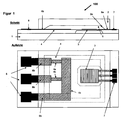
- FIG. 1 shows schematically in the upper part of the picture the construction of a test structure 100 in cross section.
- the test structure 100 comprises a base plate 1 or a region thereof, which may be provided, for example, in the form of a silicon wafer, a glass plate or another suitable carrier. Furthermore, a cover disk 2 or a region thereof with depressions 2a is arranged above the base disk 1 such that a cavity or a cavity 5 is formed.
- a pressure-sensitive sensor structure 3 is arranged, which is connected by means of interconnects 6a with corresponding contacting islands 7.
- the interconnects 6a are formed such that they form an electrical connection to the pressure-sensitive sensor structure 3 from the contacting islands 7 lying outside the cavity 5, the hermetic tightness of the cavity 5 being essentially maintained.
- the test structure 100 comprises a melt structure 4 which has one or more desired melting points.
- the melt structure 5 is shown with two desired melting points 4a, 4b, wherein in other embodiments, one or more than two desired melting points 4a, 4b may be provided.
- the enamel structure 4 is made of metal, for example aluminum, so that it is possible here to make use of well-proven metallization processes in the production of the structure 4, which are known in the state of the art of semiconductor technology.
- the conductor guide in the desired melting points 4a, 4b may be provided meandering.
- the desired melting points 4a, 4b are connected via a common electrode 4c and a plurality of interconnects 6b to corresponding contacting islands 8.
- the desired melting points 4a, 4b can optionally individually or jointly by applying a suitable voltage between the directly connected to the common electrode 4c Kunststoffierinsel 8 and with the corresponding desired melting points 4a, 4b directly connected Contacting islands 8 are activated.
- the interconnects 6b form a connection between the contacting islands 8 and the desired melting points 4a, 4b and the counterelectrode 4c in such a way that the tightness of the cavity 5 is essentially preserved.
- test structure 100 In the manufacture of the test structure 100, in the connection of the base plate 1 with the cover plate 2, the cavity 5 is provided, in which the melt structure 4 and the pressure-sensitive structure 3 are then arranged together, these previously on the base plate 1 by known from semiconductor technology manufacturing process were formed.
- the test structures 100 can be provided in numerous forms on the base plate 1, wherein the number and the position of the test structures 100 can be based on the principles of quality control, for example, if the test structures 100 are to be used for quality monitoring in the production of laminated composite structures, contain the corresponding MEMS structures, which also have a cavity whose tightness it is necessary to check.
- FIG. 2 schematically illustrates a top view of a typical compound wafer 200 as may be used to fabricate MEMS structures and test structures of the present invention.
- a plurality of test structures 100 are arranged distributed over the disk 200 in order to be able to determine local fluctuations of the entire production process for the disk 200, if necessary.
- one or more MEMS structures 201 are also provided, which may also have a cavity, similar to the cavity 5 of FIG. 1, in which a micromechanical sensor element may be arranged.
- an association 203 each consisting of a test structure 100 and a MEMS 201 is shown in each case, so that when a singling of the individual functional elements of the disc 200, for example, a test structure 100 is obtained together with a MEMS 201 as a functional unit.
- the test structures 100 are distributed with regard to available chip area as well as the highest possible statistical relevance of corresponding measurement results.
- the disc 200 may have only test structures 100 or test structures 100 and MEMS 201 in common, with the test structures 100 being provided individually during the singulation, so that they can then be provided for further applications.
- process parameter fluctuations may occur that may affect the manufacturing process.
- the importance or the influence of the individual process parameters may not be accurately predicted, so that an assessment of the state of the component during certain production phases can provide information about the importance of individual process parameters.
- the status of the functional entity and thus of the MEMS 201 can be determined by measurement data that can be obtained by operating the test structure 100. In particular, this makes it possible to achieve online monitoring of the MEMS 201.
- a suitable current is impressed via selected interconnects 6b of the enamel structure 4, so that the correspondingly controlled desired melting point 4a, 4b melts and thereby evaporates.
- a suitable current is impressed via selected interconnects 6b of the enamel structure 4, so that the correspondingly controlled desired melting point 4a, 4b melts and thereby evaporates.
- FIG. 1 shows a voltage to the uppermost and the lowest contacting island 8
- a corresponding current flow through the desired melting point 4 a can take place.
- electrical signals representing the pressure in the interior of the cavity 5 can be obtained, the course of the pressure due to the melt Hints are about the tightness of the cavity 5.
- D. h. The time course of the measured pressure values provides information about the tightness of the disc connection.
- the quality of the impermeability of the cavity 5 can be evaluated, from which a conclusion can be drawn regarding the tightness of corresponding cavities in the MEMS 201.
- the distribution of the test structures 100 on the disc, such as the disc 200 may be made to accommodate the principles of manufacturing control when using the method of quality monitoring in MEMS disc fabrication.
- the test structure 100 can also be used as a singulated element or it can be used together with the MEMS 201 as the association 203, so that it can serve as so-called online monitoring in parallel use in safety-relevant MEMS components.
- the test structure 100 When the test structure 100 is operated, if a plurality of desired melting points 4a, 4b are provided in it, these can be melted simultaneously or selectively. In one mode of operation, for example, the desired melting points 4a, 4b from FIG. 1 can be melted in chronological succession, so that corresponding measurement results can be determined at different times. To this In this way, both an efficient online monitoring of MEMS components can be realized, as well as a very efficient monitoring of the manufacturing process as well as an evaluation of the reliability of the disk connection. For this purpose, the test structure 100 can be subjected to a load test in which predetermined stress conditions are set in order to investigate the corresponding effects on the behavior of the test structure 100 and thus possibly on the MEMS 201.
- the test structure 100 may be used to evaluate the tightness of the cavity 5, from which further indications about the reliability of the test structure 100 and thus the wafer connection 200 can be obtained by using the desired melting point 4a in a first predetermined state. Thereafter, predetermined stress conditions can be exerted, for example, the disc can be operated or maintained at high or low temperatures, at high and low humidity, under the action of mechanical forces, etc. During or after such action of a predetermined stress situation, the test structure 100 can be operated again by means of the desired melting point 4b, in order thereby to have a corresponding influence of the stress situation on the reliability of the test structure 100 and thus of the disk connection 200 and / or the MEMS 201 determine. Of course, such stress examinations can also be carried out with only a single desired melting point.
- a method for evaluating the tightness of disk connections in particular in the bonding of disks for the production of micro-electro-mechanical structures (MEMS), in which the micro-mechanical sensor part is in a hermetically sealed cavity (cavity) 5, is further characterized in that micromechanical sensor structures 3 and adjacently to these melt structures 4 with electrical interconnects 6 and contact electrodes 7 and 8 located outside the cavity are produced at specific locations in certain locations in addition to the MEMS, such that in each case a micromechanical sensor 3 and a fusible structure 4 follow the disk connection with the cover plates 2 forming the cavities for the MEMS and the test structure come to lie in one and the same cavity 5, that after the disk connection process for the purpose of tightness test via the electrical external contacts 8 by means of a current the melt structure 4 for Melting is brought, whereby a pressure change in the inner region of the cavity 5 is generated, which is measured over time with the aid of the sensor structure 3.
- MEMS micro-electro-mechanical structures
- the under the modified pressure test structure is stressed specifically (temperature / humidity / mechanical, etc.) and it is by comparing the Measured values of the pressure-sensitive structure 3 before and after the stress Reliability statements obtained.
- a test structure which operates according to the preceding method, is characterized in that the melt structure 4 consists of metal, and the current-melting parts in the inner region 5 meander.
- test structure is aluminum
- the fuselage structure 4 there are multiple fuses in the fuselage structure 4, the desired fuses being defined by the design of the structure, whereby the fusing operation may be repeated in a limited number of successions.
Landscapes
- Physics & Mathematics (AREA)
- General Physics & Mathematics (AREA)
- Engineering & Computer Science (AREA)
- Manufacturing & Machinery (AREA)
- Microelectronics & Electronic Packaging (AREA)
- Micromachines (AREA)
- Pressure Sensors (AREA)
- Measuring Fluid Pressure (AREA)
- Investigating Or Analysing Biological Materials (AREA)
- Sealing Material Composition (AREA)
- Mechanical Treatment Of Semiconductor (AREA)
- Adhesives Or Adhesive Processes (AREA)
Claims (17)
- Procédé pour évaluer l'étanchéité d'un assemblage de plaques (200), lequel procédé comprend:- la fabrication d'une structure d'essai (100)-- en formant une structure de capteur micromécanique (3) et une structure de fusion adjacente (4) comprenant des pistes conductrices d'électricité (6a, 6b) et des premiers îlots de contact (7), qui sont connectés à la structure de capteur micromécanique (3), et des seconds îlots de contact (8), qui sont connectés à la structure de fusion (4), sur une plaque de base (1) ;-- en ménageant une cavité (5) par assemblage d'une plaque de couverture (2) avec la plaque de base (1), de sorte que la structure de capteur micromécanique (3) et la structure de fusion (4) se trouvent dans la cavité (5) ;- l'application d'un courant dans les seconds îlots de contact (8) pour amener la structure de fusion (4) à fondre dans le but de vérifier l'étanchéité de la cavité (5), ce qui entraîne une modification de pression dans la zone interne de la cavité (5), laquelle modification présente une variation en fonction du temps, qui est mesurée à l'aide de la structure de capteur micromécanique (3).
- Procédé selon la revendication 1, comprenant en outre la fabrication de multiples structures microélectromécaniques (201) sur l'assemblage de plaques (200).
- Procédé selon la revendication 2, dans lequel on fabrique de multiples structures d'essai (100) en des points déterminés de l'assemblage de plaques (200).
- Procédé selon la revendication 3, dans lequel les multiples structures d'essai (100) sont aménagées en fonction de critères prédéterminés de surveillance de qualité pour les structures microélectromécaniques (201).
- Procédé selon l'une quelconque des revendications 1 à 5, dans lequel la structure d'essai (100) placée sous l'action de la modification de pression est soumise à des conditions de stress déterminées et dans lequel des données de fiabilité sont récoltées par comparaison des valeurs de mesure de la structure de capteur micromécanique (3) avant et après l'exposition à la condition de stress.
- Procédé de surveillance du fonctionnement d'une structure microélectromécanique (201), lequel procédé comprend :- la fabrication d'une structure d'essai (100)-- en formant une structure de capteur micromécanique (3) et une structure de fusion adjacente (4) comprenant des pistes conductrices d'électricité (6a, 6b) et des premiers îlots de contact (7), qui sont connectés à la structure de capteur micromécanique (3), et des seconds îlots de contact (8), qui sont connectés à la structure de fusion (4), sur une plaque de base (1) ;-- en ménageant une cavité (5) par assemblage d'une plaque de couverture (2) avec la plaque de base (1), de sorte que la structure de capteur micromécanique (3) et la structure de fusion (4) se trouvent dans la cavité (5);- la fabrication de la structure microélectromécanique (201), de sorte que celle-ci forme un assemblage fonctionnel avec la structure d'essai (100) ;- le fonctionnement de la structure microélectromécanique (201) ;- l'application d'un courant dans la structure de fusion (4) de la structure d'essai (100) ; et- l'exploitation des valeurs mesurées pour la structure de capteur micromécanique (3) afin d'assurer une surveillance en ligne de la structure microélectromécanique (201).
- Procédé selon la revendication 6, dans lequel la structure de fusion (4) de la structure d'essai (100) présente plusieurs points de fusion théoriques (4a, 4b), et lequel procédé comprend en outre : le déclenchement d'un processus de fusion des multiples points de fusion théoriques, l'un après l'autre, et l'évaluation des résultats de mesure, qui sont reçus par la structure de capteur micromécanique (3) afin d'assurer la surveillance en ligne.
- Structure d'essai pour évaluer l'étanchéité d'un assemblage de plaques, comprenant:- une zone formée d'une plaque de base (1) et une zone formée d'une plaque de couverture (2),- une cavité (5), qui est formée par un assemblage de la plaque de base (1) et de la plaque de couverture (2),- une structure micromécanique sensible à la pression (3), qui est placée dans la cavité (5),- une structure de fusion (4) qui est placée dans la cavité (5),- des premiers îlots de contact (7), qui se situent en dehors de la cavité (5) et sont connectés à la structure micromécanique sensible à la pression (3),- des seconds îlots de contact (8), qui sont disposés en dehors de la cavité (5) et sont connectés à la structure de fusion (4),- des pistes conductrices (6a, 6b), qui forment une connexion entre la structure de fusion (4) et les seconds îlots de contact (8) et entre la structure micromécanique sensible à la pression (3) et les premiers îlots de contact (7).
- Structure d'essai selon la revendication 8, dans laquelle la structure de fusion comprend un point de fusion théorique (4a, 4b).
- Structure d'essai selon l'une quelconque des revendications 8 et/ou 9, dans laquelle la structure de fusion est constituée de métal.
- Structure d'essai selon la revendication 10, dans laquelle le métal contient de l'aluminium.
- Structure d'essai selon la revendication 11, dans laquelle des parties de la structure de fusion (4) fondant sous l'influence d'un courant électrique s'écoulent en méandres dans la cavité (5).
- Structure d'essai selon au moins l'une quelconque des revendications 8 à 12, dans laquelle plusieurs points de fusion théoriques (4a, 4b) sont prévus dans la structure de fusion (4) et dans laquelle les points de fusion théoriques (4a, 4b) sont définis par le modèle de la structure de fusion (4), ce qui permet de répéter successivement une opération de fusion en nombre limité.
- Assemblage de plaques (200), comprenant :- une structure d'essai (100) pour évaluer l'étanchéité de l'assemblage de plaques (200) avec-- une plaque de base (1) et une plaque de couverture (2) ;-- une cavité (5), qui est formée par assemblage de la plaque de base (1) et de la plaque de couverture (2) ;-- une structure micromécanique sensible à la pression (3), qui est placée dans la cavité (5) ;-- une structure de fusion (4), qui est placée dans la cavité (5) ;-- des premiers îlots de contact (7), qui se situent en dehors de la cavité (5) et sont connectés à la structure micromécanique sensible à la pression (3);-- des seconds îlots de contact (8), qui sont disposés en dehors de la cavité (5) et sont connectés à la structure de fusion (4) ; et-- des pistes conductrices (6a, 6b), qui forment une connexion entre la structure de fusion (4) et les seconds îlots de contact (8) et entre la structure micromécanique sensible à la pression (3) et les premiers îlots de contact (7),- une structure microélectromécanique (201).
- Assemblage de plaques selon la revendication 14, dans lequel on prévoit de multiples structures d'essai (100) et de multiples structures microélectromécaniques (201).
- Assemblage de plaques selon la revendication 15, dans lequel on aménage les multiples structures d'essai (100) en fonction des critères de surveillance de qualité des multiples structures microélectromécaniques (201).
- Assemblage de plaques selon la revendication 14 ou 15, dans lequel la structure d'essai (100) et la structure microélectromécanique (201) sont aménagées sous la forme d'un assemblage.
Applications Claiming Priority (2)
| Application Number | Priority Date | Filing Date | Title |
|---|---|---|---|
| DE102004011035A DE102004011035B4 (de) | 2004-03-06 | 2004-03-06 | Verfahren zur Prüfung der Dichtigkeit von Scheibenbondverbindungen und Anordnung zur Durchführung des Verfahrens |
| PCT/EP2005/050993 WO2005085791A1 (fr) | 2004-03-06 | 2005-03-05 | Verification de l'etancheite de connexions de plaquettes par metallisation, et structure de verification servant a la mise en oeuvre ce procede |
Publications (2)
| Publication Number | Publication Date |
|---|---|
| EP1723402A1 EP1723402A1 (fr) | 2006-11-22 |
| EP1723402B1 true EP1723402B1 (fr) | 2007-07-18 |
Family
ID=34877487
Family Applications (1)
| Application Number | Title | Priority Date | Filing Date |
|---|---|---|---|
| EP05729617A Expired - Lifetime EP1723402B1 (fr) | 2004-03-06 | 2005-03-05 | Verification de l'etancheite des connexions de plaquettes par metallisation, et structure de verification servant a la mise en oeuvre de ce procede |
Country Status (6)
| Country | Link |
|---|---|
| US (1) | US7520161B2 (fr) |
| EP (1) | EP1723402B1 (fr) |
| AT (1) | ATE367574T1 (fr) |
| DE (2) | DE102004011035B4 (fr) |
| DK (1) | DK1723402T3 (fr) |
| WO (1) | WO2005085791A1 (fr) |
Families Citing this family (8)
| Publication number | Priority date | Publication date | Assignee | Title |
|---|---|---|---|---|
| JP2011218462A (ja) * | 2010-04-06 | 2011-11-04 | Seiko Epson Corp | Mems装置 |
| US8921128B2 (en) * | 2013-05-29 | 2014-12-30 | Analog Devices, Inc. | Method of manufacturing MEMS devices with reliable hermetic seal |
| US9054223B2 (en) | 2013-06-17 | 2015-06-09 | Knowles Electronics, Llc | Varistor in base for MEMS microphones |
| CN106449269B (zh) * | 2016-10-12 | 2018-09-14 | 厦门大学 | 一种压力敏感结构以及制备该压力敏感结构的方法 |
| CN111762754B (zh) * | 2020-06-30 | 2024-06-18 | 上海华虹宏力半导体制造有限公司 | 测量共晶键合对准偏差的测试结构 |
| CN112504546B (zh) * | 2020-11-11 | 2022-09-06 | 中国电子产品可靠性与环境试验研究所((工业和信息化部电子第五研究所)(中国赛宝实验室)) | 晶圆级气密封装的微小腔体内部气压测试方法和系统 |
| CN116072563A (zh) * | 2021-10-29 | 2023-05-05 | 长鑫存储技术有限公司 | 半导体结构及其制备方法、测试系统 |
| CN116852399B (zh) * | 2023-09-05 | 2023-11-17 | 陕西能控安远智能技术有限公司 | 一种多用途防爆机器人 |
Family Cites Families (8)
| Publication number | Priority date | Publication date | Assignee | Title |
|---|---|---|---|---|
| DE19638666C1 (de) * | 1996-01-08 | 1997-11-20 | Siemens Ag | Schmelzsicherung mit einer Schutzschicht in einer integrierten Halbleiterschaltung sowie zugehöriges Herstellungsverfahren |
| US5837935A (en) | 1996-02-26 | 1998-11-17 | Ford Motor Company | Hermetic seal for an electronic component having a secondary chamber |
| DE19700734B4 (de) * | 1997-01-11 | 2006-06-01 | Robert Bosch Gmbh | Verfahren zur Herstellung von Sensoren sowie nicht-vereinzelter Waferstapel |
| DE19739961C1 (de) * | 1997-09-11 | 1999-04-15 | Siemens Ag | Verfahren zur Bestimmung des Gasdruckes in einem Hohlraum mit verformbarer Wandung eines Halbleiterbauelementes |
| EP0951068A1 (fr) * | 1998-04-17 | 1999-10-20 | Interuniversitair Micro-Elektronica Centrum Vzw | Procédé de fabrication pour une microstructure avec une cavité interne |
| US6232150B1 (en) * | 1998-12-03 | 2001-05-15 | The Regents Of The University Of Michigan | Process for making microstructures and microstructures made thereby |
| US6638784B2 (en) * | 1999-06-24 | 2003-10-28 | Rockwell Collins, Inc. | Hermetic chip scale packaging means and method including self test |
| DE10136219A1 (de) * | 2001-07-25 | 2003-02-06 | Conti Temic Microelectronic | Verfahren zur Dichtigkeitsprüfung von kapazitiven Sensoren |
-
2004
- 2004-03-06 DE DE102004011035A patent/DE102004011035B4/de not_active Expired - Fee Related
-
2005
- 2005-03-05 WO PCT/EP2005/050993 patent/WO2005085791A1/fr not_active Ceased
- 2005-03-05 AT AT05729617T patent/ATE367574T1/de not_active IP Right Cessation
- 2005-03-05 DK DK05729617T patent/DK1723402T3/da active
- 2005-03-05 DE DE502005001067T patent/DE502005001067D1/de not_active Expired - Fee Related
- 2005-03-05 EP EP05729617A patent/EP1723402B1/fr not_active Expired - Lifetime
- 2005-03-05 US US10/591,686 patent/US7520161B2/en not_active Expired - Fee Related
Also Published As
| Publication number | Publication date |
|---|---|
| ATE367574T1 (de) | 2007-08-15 |
| DE502005001067D1 (de) | 2007-08-30 |
| US7520161B2 (en) | 2009-04-21 |
| DE102004011035B4 (de) | 2006-05-04 |
| DE102004011035A1 (de) | 2005-09-22 |
| EP1723402A1 (fr) | 2006-11-22 |
| DK1723402T3 (da) | 2007-10-15 |
| US20070196943A1 (en) | 2007-08-23 |
| WO2005085791A1 (fr) | 2005-09-15 |
Similar Documents
| Publication | Publication Date | Title |
|---|---|---|
| DE19700734B4 (de) | Verfahren zur Herstellung von Sensoren sowie nicht-vereinzelter Waferstapel | |
| DE69912376T2 (de) | Verfahren zur herstellung eines halbleiterbauelements | |
| DE19734530B4 (de) | Halbleiterbeschleunigungssensor | |
| DE102005001449B3 (de) | Verfahren zum Erzeugen eines vorgegebenen Innendrucks in einem Hohlraum eines Halbleiterbauelements | |
| EP1440322A1 (fr) | Microcapteur | |
| DE10323668A1 (de) | Intergrierter Schaltkreischip und Wafer sowie Prüfverfahren und -vorrichtung | |
| EP2921833B1 (fr) | Capteur thermo-analytique et procédé destiné à sa fabrication | |
| DE602004010116T2 (de) | Verfahren und vorrichtung zum testen elektrischer eigenschaften eines zu prüfenden objekts | |
| DE102015103286A1 (de) | System und Verfahren für eine mikrofabrizierte Bruchteststruktur | |
| EP1723402B1 (fr) | Verification de l'etancheite des connexions de plaquettes par metallisation, et structure de verification servant a la mise en oeuvre de ce procede | |
| DE102011086479A1 (de) | Integrierter Feuchtesensor und Verfahren zu dessen Herstellung | |
| WO2018069028A1 (fr) | Capteur micro-mécanique à structure de découplage de contraintes | |
| DE102007020257B4 (de) | Vereinheitlichte Teststruktur für belastungsabhängige Materialwanderungsprüfungen | |
| WO1999049285A1 (fr) | Composant detecteur | |
| DE60025214T2 (de) | Mikrodeckelgehäuse auf Scheibenebene | |
| DE102019127649A1 (de) | Halbleiterbauelement und Anordnung zur Kontaktierung des Halbleiterbauelements beim anodischen Bonden eines Glassubstrats mit Kontaktdurchführungen an ein Siliziumsubstrat | |
| DE10257097B4 (de) | Verfahren zur Herstellung von mikroelektromechanischen Systemen (Microelectromechanical Systems: MEMS) mittels Silizium-Hochtemperatur-Fusionsbonden | |
| DE102016222243A1 (de) | Gassensor | |
| EP2714582B1 (fr) | Procédé de fabrication d'un transistor mos | |
| DE19931773C1 (de) | Mikromechanisches Bauelement mit Kontaktdurchführungen, sowie Verfahren zur Herstellung eines mikromechanischen Bauelements | |
| DE19832681A1 (de) | Sensor, Sensoranordnung und deren Verwendung | |
| DE102021204645A1 (de) | Verfahren zur Herstellung eines mikroelektromechanischen Sensors aus einem MEMS-Element und einem ASIC-Element und mikroelektromechanischer Sensor | |
| DE19710375C2 (de) | Verfahren zum Herstellen von räumlich strukturierten Bauteilen | |
| DE19944410C2 (de) | Vorrichtung zur Halterung einer zu heizenden Mikrostruktur und Verfahren zur Herstellung der Vorrichtung | |
| DE102024120164A1 (de) | Gassensorchip für wärmeleitfähigkeitsmessungen sowie verfahren zur herstellung und zum betrieb eines solchen |
Legal Events
| Date | Code | Title | Description |
|---|---|---|---|
| PUAI | Public reference made under article 153(3) epc to a published international application that has entered the european phase |
Free format text: ORIGINAL CODE: 0009012 |
|
| 17P | Request for examination filed |
Effective date: 20060613 |
|
| AK | Designated contracting states |
Kind code of ref document: A1 Designated state(s): AT BE BG CH CY CZ DE DK EE ES FI FR GB GR HU IE IS IT LI LT LU MC NL PL PT RO SE SI SK TR |
|
| GRAP | Despatch of communication of intention to grant a patent |
Free format text: ORIGINAL CODE: EPIDOSNIGR1 |
|
| DAX | Request for extension of the european patent (deleted) | ||
| GRAS | Grant fee paid |
Free format text: ORIGINAL CODE: EPIDOSNIGR3 |
|
| GRAA | (expected) grant |
Free format text: ORIGINAL CODE: 0009210 |
|
| AK | Designated contracting states |
Kind code of ref document: B1 Designated state(s): AT BE BG CH CY CZ DE DK EE ES FI FR GB GR HU IE IS IT LI LT LU MC NL PL PT RO SE SI SK TR |
|
| REG | Reference to a national code |
Ref country code: GB Ref legal event code: FG4D Free format text: NOT ENGLISH |
|
| REG | Reference to a national code |
Ref country code: CH Ref legal event code: EP |
|
| REF | Corresponds to: |
Ref document number: 502005001067 Country of ref document: DE Date of ref document: 20070830 Kind code of ref document: P |
|
| REG | Reference to a national code |
Ref country code: IE Ref legal event code: FG4D Free format text: LANGUAGE OF EP DOCUMENT: GERMAN |
|
| REG | Reference to a national code |
Ref country code: DK Ref legal event code: T3 |
|
| REG | Reference to a national code |
Ref country code: CH Ref legal event code: NV Representative=s name: ISLER & PEDRAZZINI AG |
|
| GBT | Gb: translation of ep patent filed (gb section 77(6)(a)/1977) |
Effective date: 20071004 |
|
| ET | Fr: translation filed | ||
| PG25 | Lapsed in a contracting state [announced via postgrant information from national office to epo] |
Ref country code: BG Free format text: LAPSE BECAUSE OF FAILURE TO SUBMIT A TRANSLATION OF THE DESCRIPTION OR TO PAY THE FEE WITHIN THE PRESCRIBED TIME-LIMIT Effective date: 20071018 Ref country code: NL Free format text: LAPSE BECAUSE OF FAILURE TO SUBMIT A TRANSLATION OF THE DESCRIPTION OR TO PAY THE FEE WITHIN THE PRESCRIBED TIME-LIMIT Effective date: 20070718 Ref country code: PT Free format text: LAPSE BECAUSE OF FAILURE TO SUBMIT A TRANSLATION OF THE DESCRIPTION OR TO PAY THE FEE WITHIN THE PRESCRIBED TIME-LIMIT Effective date: 20071218 Ref country code: FI Free format text: LAPSE BECAUSE OF FAILURE TO SUBMIT A TRANSLATION OF THE DESCRIPTION OR TO PAY THE FEE WITHIN THE PRESCRIBED TIME-LIMIT Effective date: 20070718 Ref country code: IS Free format text: LAPSE BECAUSE OF FAILURE TO SUBMIT A TRANSLATION OF THE DESCRIPTION OR TO PAY THE FEE WITHIN THE PRESCRIBED TIME-LIMIT Effective date: 20071118 Ref country code: LT Free format text: LAPSE BECAUSE OF FAILURE TO SUBMIT A TRANSLATION OF THE DESCRIPTION OR TO PAY THE FEE WITHIN THE PRESCRIBED TIME-LIMIT Effective date: 20070718 Ref country code: ES Free format text: LAPSE BECAUSE OF FAILURE TO SUBMIT A TRANSLATION OF THE DESCRIPTION OR TO PAY THE FEE WITHIN THE PRESCRIBED TIME-LIMIT Effective date: 20071029 |
|
| NLV1 | Nl: lapsed or annulled due to failure to fulfill the requirements of art. 29p and 29m of the patents act | ||
| PG25 | Lapsed in a contracting state [announced via postgrant information from national office to epo] |
Ref country code: PL Free format text: LAPSE BECAUSE OF FAILURE TO SUBMIT A TRANSLATION OF THE DESCRIPTION OR TO PAY THE FEE WITHIN THE PRESCRIBED TIME-LIMIT Effective date: 20070718 |
|
| REG | Reference to a national code |
Ref country code: IE Ref legal event code: FD4D |
|
| PG25 | Lapsed in a contracting state [announced via postgrant information from national office to epo] |
Ref country code: GR Free format text: LAPSE BECAUSE OF FAILURE TO SUBMIT A TRANSLATION OF THE DESCRIPTION OR TO PAY THE FEE WITHIN THE PRESCRIBED TIME-LIMIT Effective date: 20071019 |
|
| PGFP | Annual fee paid to national office [announced via postgrant information from national office to epo] |
Ref country code: DK Payment date: 20080308 Year of fee payment: 4 |
|
| PLBE | No opposition filed within time limit |
Free format text: ORIGINAL CODE: 0009261 |
|
| STAA | Information on the status of an ep patent application or granted ep patent |
Free format text: STATUS: NO OPPOSITION FILED WITHIN TIME LIMIT |
|
| PG25 | Lapsed in a contracting state [announced via postgrant information from national office to epo] |
Ref country code: CZ Free format text: LAPSE BECAUSE OF FAILURE TO SUBMIT A TRANSLATION OF THE DESCRIPTION OR TO PAY THE FEE WITHIN THE PRESCRIBED TIME-LIMIT Effective date: 20070718 Ref country code: SK Free format text: LAPSE BECAUSE OF FAILURE TO SUBMIT A TRANSLATION OF THE DESCRIPTION OR TO PAY THE FEE WITHIN THE PRESCRIBED TIME-LIMIT Effective date: 20070718 Ref country code: IE Free format text: LAPSE BECAUSE OF FAILURE TO SUBMIT A TRANSLATION OF THE DESCRIPTION OR TO PAY THE FEE WITHIN THE PRESCRIBED TIME-LIMIT Effective date: 20070718 |
|
| 26N | No opposition filed |
Effective date: 20080421 |
|
| PG25 | Lapsed in a contracting state [announced via postgrant information from national office to epo] |
Ref country code: SE Free format text: LAPSE BECAUSE OF FAILURE TO SUBMIT A TRANSLATION OF THE DESCRIPTION OR TO PAY THE FEE WITHIN THE PRESCRIBED TIME-LIMIT Effective date: 20071018 Ref country code: RO Free format text: LAPSE BECAUSE OF FAILURE TO SUBMIT A TRANSLATION OF THE DESCRIPTION OR TO PAY THE FEE WITHIN THE PRESCRIBED TIME-LIMIT Effective date: 20070718 |
|
| PGFP | Annual fee paid to national office [announced via postgrant information from national office to epo] |
Ref country code: AT Payment date: 20080319 Year of fee payment: 4 |
|
| PGFP | Annual fee paid to national office [announced via postgrant information from national office to epo] |
Ref country code: BE Payment date: 20080317 Year of fee payment: 4 |
|
| PG25 | Lapsed in a contracting state [announced via postgrant information from national office to epo] |
Ref country code: MC Free format text: LAPSE BECAUSE OF NON-PAYMENT OF DUE FEES Effective date: 20080331 |
|
| PGFP | Annual fee paid to national office [announced via postgrant information from national office to epo] |
Ref country code: FR Payment date: 20080328 Year of fee payment: 4 |
|
| PG25 | Lapsed in a contracting state [announced via postgrant information from national office to epo] |
Ref country code: EE Free format text: LAPSE BECAUSE OF FAILURE TO SUBMIT A TRANSLATION OF THE DESCRIPTION OR TO PAY THE FEE WITHIN THE PRESCRIBED TIME-LIMIT Effective date: 20070718 |
|
| PG25 | Lapsed in a contracting state [announced via postgrant information from national office to epo] |
Ref country code: SI Free format text: LAPSE BECAUSE OF FAILURE TO SUBMIT A TRANSLATION OF THE DESCRIPTION OR TO PAY THE FEE WITHIN THE PRESCRIBED TIME-LIMIT Effective date: 20070718 |
|
| PG25 | Lapsed in a contracting state [announced via postgrant information from national office to epo] |
Ref country code: CY Free format text: LAPSE BECAUSE OF FAILURE TO SUBMIT A TRANSLATION OF THE DESCRIPTION OR TO PAY THE FEE WITHIN THE PRESCRIBED TIME-LIMIT Effective date: 20070718 |
|
| BERE | Be: lapsed |
Owner name: X-FAB SEMICONDUCTOR FOUNDRIES A.G. Effective date: 20090331 |
|
| PG25 | Lapsed in a contracting state [announced via postgrant information from national office to epo] |
Ref country code: AT Free format text: LAPSE BECAUSE OF NON-PAYMENT OF DUE FEES Effective date: 20090305 |
|
| REG | Reference to a national code |
Ref country code: CH Ref legal event code: PL |
|
| REG | Reference to a national code |
Ref country code: DK Ref legal event code: EBP |
|
| GBPC | Gb: european patent ceased through non-payment of renewal fee |
Effective date: 20090305 |
|
| REG | Reference to a national code |
Ref country code: FR Ref legal event code: ST Effective date: 20091130 |
|
| PG25 | Lapsed in a contracting state [announced via postgrant information from national office to epo] |
Ref country code: CH Free format text: LAPSE BECAUSE OF NON-PAYMENT OF DUE FEES Effective date: 20090331 Ref country code: LI Free format text: LAPSE BECAUSE OF NON-PAYMENT OF DUE FEES Effective date: 20090331 |
|
| PGFP | Annual fee paid to national office [announced via postgrant information from national office to epo] |
Ref country code: DE Payment date: 20090930 Year of fee payment: 5 |
|
| PG25 | Lapsed in a contracting state [announced via postgrant information from national office to epo] |
Ref country code: BE Free format text: LAPSE BECAUSE OF NON-PAYMENT OF DUE FEES Effective date: 20090331 |
|
| PG25 | Lapsed in a contracting state [announced via postgrant information from national office to epo] |
Ref country code: FR Free format text: LAPSE BECAUSE OF NON-PAYMENT OF DUE FEES Effective date: 20091123 Ref country code: DK Free format text: LAPSE BECAUSE OF NON-PAYMENT OF DUE FEES Effective date: 20090331 Ref country code: GB Free format text: LAPSE BECAUSE OF NON-PAYMENT OF DUE FEES Effective date: 20090305 |
|
| PG25 | Lapsed in a contracting state [announced via postgrant information from national office to epo] |
Ref country code: HU Free format text: LAPSE BECAUSE OF FAILURE TO SUBMIT A TRANSLATION OF THE DESCRIPTION OR TO PAY THE FEE WITHIN THE PRESCRIBED TIME-LIMIT Effective date: 20080119 Ref country code: LU Free format text: LAPSE BECAUSE OF NON-PAYMENT OF DUE FEES Effective date: 20080305 |
|
| PG25 | Lapsed in a contracting state [announced via postgrant information from national office to epo] |
Ref country code: TR Free format text: LAPSE BECAUSE OF FAILURE TO SUBMIT A TRANSLATION OF THE DESCRIPTION OR TO PAY THE FEE WITHIN THE PRESCRIBED TIME-LIMIT Effective date: 20070718 |
|
| PG25 | Lapsed in a contracting state [announced via postgrant information from national office to epo] |
Ref country code: DE Free format text: LAPSE BECAUSE OF NON-PAYMENT OF DUE FEES Effective date: 20101001 |
|
| PGFP | Annual fee paid to national office [announced via postgrant information from national office to epo] |
Ref country code: IT Payment date: 20080331 Year of fee payment: 4 |