EP1722413A2 - Terminal connection structure for semiconductor device - Google Patents
Terminal connection structure for semiconductor device Download PDFInfo
- Publication number
- EP1722413A2 EP1722413A2 EP06113040A EP06113040A EP1722413A2 EP 1722413 A2 EP1722413 A2 EP 1722413A2 EP 06113040 A EP06113040 A EP 06113040A EP 06113040 A EP06113040 A EP 06113040A EP 1722413 A2 EP1722413 A2 EP 1722413A2
- Authority
- EP
- European Patent Office
- Prior art keywords
- semiconductor device
- pair
- wiring member
- electrode terminals
- joint
- Prior art date
- Legal status (The legal status is an assumption and is not a legal conclusion. Google has not performed a legal analysis and makes no representation as to the accuracy of the status listed.)
- Granted
Links
Images


Classifications
-
- H—ELECTRICITY
- H10—SEMICONDUCTOR DEVICES; ELECTRIC SOLID-STATE DEVICES NOT OTHERWISE PROVIDED FOR
- H10W—GENERIC PACKAGES, INTERCONNECTIONS, CONNECTORS OR OTHER CONSTRUCTIONAL DETAILS OF DEVICES COVERED BY CLASS H10
- H10W90/00—Package configurations
-
- H—ELECTRICITY
- H01—ELECTRIC ELEMENTS
- H01G—CAPACITORS; CAPACITORS, RECTIFIERS, DETECTORS, SWITCHING DEVICES, LIGHT-SENSITIVE OR TEMPERATURE-SENSITIVE DEVICES OF THE ELECTROLYTIC TYPE
- H01G4/00—Fixed capacitors; Processes of their manufacture
- H01G4/002—Details
- H01G4/228—Terminals
-
- H—ELECTRICITY
- H10—SEMICONDUCTOR DEVICES; ELECTRIC SOLID-STATE DEVICES NOT OTHERWISE PROVIDED FOR
- H10W—GENERIC PACKAGES, INTERCONNECTIONS, CONNECTORS OR OTHER CONSTRUCTIONAL DETAILS OF DEVICES COVERED BY CLASS H10
- H10W44/00—Electrical arrangements for controlling or matching impedance
- H10W44/501—Inductive arrangements
-
- H—ELECTRICITY
- H02—GENERATION; CONVERSION OR DISTRIBUTION OF ELECTRIC POWER
- H02M—APPARATUS FOR CONVERSION BETWEEN AC AND AC, BETWEEN AC AND DC, OR BETWEEN DC AND DC, AND FOR USE WITH MAINS OR SIMILAR POWER SUPPLY SYSTEMS; CONVERSION OF DC OR AC INPUT POWER INTO SURGE OUTPUT POWER; CONTROL OR REGULATION THEREOF
- H02M7/00—Conversion of AC power input into DC power output; Conversion of DC power input into AC power output
- H02M7/003—Constructional details, e.g. physical layout, assembly, wiring or busbar connections
Definitions
- the present invention relates to a terminal connection structure for a semiconductor device, and more particularly to a structure for connecting a pair of electrode terminals of an external device, in which currents flow in directions opposite to each other, with corresponding electrode terminals of the semiconductor device, respectively.
- JP 06-69415 A discloses a semiconductor device used as a power module or the like for constituting an inverter device.
- a pair of internal wiring units which are held in a case and in which currents flow in directions opposite to each other are arranged to be adjacent and opposed to each other. Due to an effect of a mutual inductance, an inductance of each of the internal wiring units is reduced.
- a positive terminal and a negative terminal connected to the pair of internal wiring units, respectively, are drawn out to the outside of the case to be disposed on a top surface of the case.
- a hole for screw mounting is provided in each of the positive terminal and the negative terminal of the semiconductor device.
- Such a semiconductor device has a pair of wiring members connected to a positive terminal and a negative terminal of an external device, respectively.
- a hole for screw mounting is also provided in each of the pair of wiring members.
- the pair of wiring members are secured by screws to the corresponding electrode terminals of the semiconductor device.
- the present invention has been made in order to solve the above-mentioned problems, and an object of the present invention is to provide a terminal connection structure for a semiconductor device capable of reducing an inductance of wiring members.
- a terminal connection structure for a semiconductor device including: a pair of electrode terminals of an external device; a pair of electrode terminals of the semiconductor device each corresponding to the pair of electrode terminals of the external device ,respectively; and a pair of wiring members each having a flat plate shape and arranged to be adjacent and opposed to each other for connecting the pair of electrode terminals of the external device with the corresponding pair of electrode terminals of the semiconductor device, respectively, and in which currents flow in directions opposite to each other, the pair of wiring members and the pair of electrode terminals of the semiconductor device being joined through ultrasonic bonding, respectively.
- FIG. 1 shows a terminal connection structure for a semiconductor device according to a first embodiment of the present invention.
- a semiconductor device 1 is used as a power module for constituting an inverter device and includes a case 2 formed of a resin or the like.
- a semiconductor circuit (not shown) is provided inside the case 2, and a positive terminal 3 and a negative terminal 4 connected to the semiconductor circuit and drawn out to the outside of the case 2 are arranged on a top surface of the case 2, respectively.
- a power capacitor 5 serving as an external device is arranged in the vicinity of the semiconductor device 1.
- a positive terminal 6 of the power capacitor 5 is electrically connected to the positive terminal 3 of the semiconductor device 1 through a first wiring member 8.
- a negative terminal 7 of the power capacitor 5 is electrically connected to the negative terminal 4 of the semiconductor device 1 through a second wiring member 9.
- the first wiring member 8 and the second wiring member 9 each have a substantially rectangular flat plate shape, and are arranged to be adjacent and opposed to each other.
- the positive terminal 6 of the power capacitor 5 is connected to one end of the first wiring member 8, and the negative terminal 7 of the power capacitor 5 is connected to one end of the second wiring member 9.
- joints 8a and 9a At the other ends of the first wiring member 8 and the second wiring member 9, there are provided joints 8a and 9a, respectively.
- the joints 8a and 9a each have a small area and are arranged so as not to overlap each other.
- the joint 8a of the first wiring member 8 and the joint 9a of the second wiring member 9 are joined to the positive terminal 3 and the negative terminal 4 of the semiconductor device 1, respectively, through ribbon bonding, which is a kind of ultrasonic bonding.
- a midpoint electrode terminal 10 is also arranged which is connected to the semiconductor circuit (not shown) in the case 2 and is drawn out to the outside of the case 2.
- the positive terminal 3 of the semiconductor device 1 is joined to a joint portion 8c of the ribbon member 8b at one end thereof, while the joint 8a of the first wiring member 8 is joined to another joint portion 8c of the ribbon member 8b at the other end thereof.
- the positive terminal 3 of the semiconductor device 1 and the first wiring member 8 are electrically connected through the ribbon member 8b. That is, it can be said that the positive terminal 3 of the semiconductor device 1 and the first wiring member 8 are joined to each other through the ribbon member 8b.
- the negative terminal 4 of the semiconductor device 1 is joined to a joint portion 9c of the ribbon member 9b at one end thereof, while the joint 9a of the second wiring member 9 is joined to another joint portion 9c of the ribbon member 9b at the other end thereof.
- the negative terminal 4 of the semiconductor device 1 and the second wiring member 9 are electrically connected through the ribbon member 9b. That is, it can be said that the negative terminal 4 of the semiconductor device 1 and the second wiring member 9 are joined to each other through the ribbon member 9b.
- Static pressure in a vertical direction is applied to the ribbon member 8b against the joint 8a of the first wiring member 8 and the positive terminal 3 of the semiconductor device 1, and oscillation is applied thereto by an ultrasonic wave oscillator, thereby causing them fictional motions to join them to each other.
- static pressure in a vertical direction is applied to the ribbon member 9b against the joint 9a of the second wiring member 9 and the negative terminal 4 of the semiconductor device 1, and oscillation is applied thereto by the ultrasonic wave oscillator, thereby causing them fictional motions to join them to each other.
- FIG. 3 inside the case 2 of the semiconductor device 1, there are two main circuit elements 11 and 12 for constituting an upper arm and a lower arm for one phase.
- the main circuit elements 11 and 12 are connected in series with each other.
- the positive terminal 3 of the semiconductor device 1 is drawn out from a point A
- the negative terminal 4 of the semiconductor device 1 is drawn out from a point B
- the midpoint electrode terminal 10 of the semiconductor device 1 is drawn out from a point C.
- first wiring member 8 and the second wiring member 9 through which thus currents flow in directions opposite to each other, each have a flat plate shape and are arranged so as to be adjacent and opposed to each other, due to an effect of a mutual inductance, an inductance of each of the first wiring member 8 and the second wiring member 9 can be reduced.
- the joint 8a of the first wiring member 8 and the joint 9a of the second wiring member 9 are joined to the positive terminal 3 and the negative terminal 4 of the semiconductor device 1, respectively, through ultrasonic bonding. Therefore, the joint 8a of the first wiring member 8 and the joint 9a of the second wiring member 9 are not required to be provided with exclusive portions for screw mounting unlike a conventional manner, so each of the joints 8a and 9a needs no large area. As a result, the inductance of each of the first wiring member 8 and the second wiring member 9 can be further reduced.
- a value of the surge voltage can be limited to be small, thereby making it possible to use semiconductor element or the like having a small withstanding voltage in the device 1. Therefore, manufacturing cost can be lowered.
- each of the positive terminal 3 and the negative terminal 4 of the semiconductor device 1 can also be formed by a member having a smaller area than that in a case of screw mounting. Therefore, it is possible to realize miniaturization of the semiconductor device 1 and reduction in manufacturing cost.
- the second embodiment is different from the above-mentioned first embodiment in that the joint 8a of the first wiring member 8 and the joint 9a of the second wiring member 9 are joined to a positive terminal 21 and a negative terminal 22 of the semiconductor device 1, respectively, through resistance welding instead of ultrasonic bonding.
- the positive terminal 21 and the negative terminal 22 of the semiconductor device 1 each have a shape protruding upwardly from the top surface of the case 2.
- the joint 8a of the first wiring member 8 and the joint 9a of the second wiring member 9 are bent upwardly to be opposed to the positive terminal 21 and the negative terminal 22, respectively.
- the first wiring member 8 and the second wiring member 9 are adjacent and opposed to each other, and the joint 8a of the first wiring member 8 and the joint 9a of the second wiring member 9 are not required to be provided with exclusive portions for screw mounting, so the joints 8a and 9a each can have a small area as in the case of the first embodiment.
- inductances of the first wiring member 8 and the second wiring member 9 can be reduced, to thereby making it possible to obtain the same effect as that in the first embodiment.
- a current i flows through the joint 8a of the first wiring member 8 in a direction opposite to a current flowing through the positive terminal 21 of the semiconductor device 1, as indicated by a dash-dotted line shown in FIG. 4.
- a current i flows through the joint 9a of the second wiring member 9 in a direction opposite to a current flowing through the negative terminal 22 of the semiconductor device 1. Consequently, inductances of those parts can also be reduced.
- joining between the joint 8a of the first wiring member 8 and the positive terminal 21 of the semiconductor device 1, and joining between the joint 9a of the second wiring member 9 and the negative terminal 22 of the semiconductor device 1 can also be performed directly through ultrasonic bonding instead of resistance welding.
- the joint 8a of the first wiring member 8 is joined to the positive terminal 3 of the semiconductor device 1, and the joint 9a of the second wiring member 9 is joined to the negative terminal 4 of the semiconductor device 1.
- the joint 8a of the first wiring member 8 and the positive terminal 3 of the semiconductor device 1 are joined to each other through solder 31, and the joint 9a of the second wiring member 9 and the negative terminal 4 of the semiconductor device 1 are joined to each other through solder 32.
- the first wiring member 8 and the second wiring member 9 are adjacent and opposed to each other, and the joint 8a of the first wiring member 8 and the joint 9a of the second wiring member 9 are not required to be provided with exclusive portions for screw mounting, so the joints 8a and 9a each can have a small area as in the case of the first embodiment.
- inductances of the firstwiringmember 8 and the second wiring member 9 can be reduced, to thereby making it possible to obtain the same effect as that in the first embodiment.
- a chopper circuit or the like may be accommodated in the case 2 of the semiconductor device 1.
- the joining method is not limited to ultrasonic bonding, resistance welding, and solder joint.
- the joint 8a of the first wiring member 8 and the joint 9a of the second wiring member 9 may be joined to the positive terminal 3 and the negative terminal 4 of the semiconductor device 1, respectively.
- the power capacitor 5 an electrolytic capacitor or other various kinds of capacitors can be used.
- the external device is not limited to the power capacitor 5. Any other kinds of devices such as DC power line can be connected as an external device as long as a device has a structure in which there are provided a pair of electrode terminals each connected to the corresponding electrode terminals of the semiconductor device through the first wiring member 8 and the second wiring member 9, respectively, and in which currents flow in directions opposite to each other through the first wiring member 8 and the second wiring member 9.
- a joint of the first wiring member and a joint of the second wiring member are joined to the positive terminal and the negative terminal of the semiconductor device through ultrasonic bonding, respectively.
- the joint of the first wiring member and the joint of the second wiring member are not required to be provided with exclusive portions for screw mounting unlike a conventional manner, so each of the joints can have a small area, to thereby making it possible to reduce inductances of the first wiring member and the second wiring member.
Landscapes
- Engineering & Computer Science (AREA)
- Power Engineering (AREA)
- Manufacturing & Machinery (AREA)
- Microelectronics & Electronic Packaging (AREA)
- Inverter Devices (AREA)
- Power Conversion In General (AREA)
- Multi-Conductor Connections (AREA)
Abstract
Description
- The present invention relates to a terminal connection structure for a semiconductor device, and more particularly to a structure for connecting a pair of electrode terminals of an external device, in which currents flow in directions opposite to each other, with corresponding electrode terminals of the semiconductor device, respectively.
- For example,
JP 06-69415 A - In addition, in the semiconductor device, a positive terminal and a negative terminal connected to the pair of internal wiring units, respectively, are drawn out to the outside of the case to be disposed on a top surface of the case. A hole for screw mounting is provided in each of the positive terminal and the negative terminal of the semiconductor device. Such a semiconductor device has a pair of wiring members connected to a positive terminal and a negative terminal of an external device, respectively. A hole for screw mounting is also provided in each of the pair of wiring members. The pair of wiring members are secured by screws to the corresponding electrode terminals of the semiconductor device. As a result, it is possible to electrically connect the positive terminal and the negative terminal of the semiconductor device with the positive terminal and the negative terminal of the external device, respectively, through the pair of wiring members.
- However, exclusive portions for screw mounting in which holes for screw mounting are formed must be provided in the pair of wiring members, respectively. In addition, since the exclusive portions for screw mounting necessary of the pair of wiring members are secured by screw to the positive terminal and the negative terminal arranged on the top surface of the case of the semiconductor device, it is impossible to arrange the pair of wiring members to be adjacent and opposed to each other as in the internal wiring units disclosed in
JP 06-69415 A - The present invention has been made in order to solve the above-mentioned problems, and an object of the present invention is to provide a terminal connection structure for a semiconductor device capable of reducing an inductance of wiring members.
- According to the present invention, there is provided a terminal connection structure for a semiconductor device, including: a pair of electrode terminals of an external device; a pair of electrode terminals of the semiconductor device each corresponding to the pair of electrode terminals of the external device ,respectively; and a pair of wiring members each having a flat plate shape and arranged to be adjacent and opposed to each other for connecting the pair of electrode terminals of the external device with the corresponding pair of electrode terminals of the semiconductor device, respectively, and in which currents flow in directions opposite to each other, the pair of wiring members and the pair of electrode terminals of the semiconductor device being joined through ultrasonic bonding, respectively.
-
- FIG. 1 is a plan view showing a terminal connection structure for a semiconductor device according to a first embodiment of the present invention;
- FIG. 2 is a perspective view showing a structure in the vicinity of terminals of the semiconductor device in the first embodiment of the present invention;
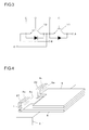
- FIG. 3 is a circuit diagram showing a structure of inside of a case in the first embodiment of the present invention.
- FIGS. 4 and 5 are perspective views showing structures in the vicinity of the terminals of the semiconductor device in a second embodiment and a third embodiment of the present invention, respectively.
- Hereinafter, embodiments of the present invention will be described with reference to the accompanying drawings.
- FIG. 1 shows a terminal connection structure for a semiconductor device according to a first embodiment of the present invention. A
semiconductor device 1 is used as a power module for constituting an inverter device and includes acase 2 formed of a resin or the like. A semiconductor circuit (not shown) is provided inside thecase 2, and apositive terminal 3 and anegative terminal 4 connected to the semiconductor circuit and drawn out to the outside of thecase 2 are arranged on a top surface of thecase 2, respectively. - In addition, a
power capacitor 5 serving as an external device is arranged in the vicinity of thesemiconductor device 1. Apositive terminal 6 of thepower capacitor 5 is electrically connected to thepositive terminal 3 of thesemiconductor device 1 through afirst wiring member 8. Anegative terminal 7 of thepower capacitor 5 is electrically connected to thenegative terminal 4 of thesemiconductor device 1 through asecond wiring member 9. In this case, thefirst wiring member 8 and thesecond wiring member 9 each have a substantially rectangular flat plate shape, and are arranged to be adjacent and opposed to each other. Thepositive terminal 6 of thepower capacitor 5 is connected to one end of thefirst wiring member 8, and thenegative terminal 7 of thepower capacitor 5 is connected to one end of thesecond wiring member 9. At the other ends of thefirst wiring member 8 and thesecond wiring member 9, there are providedjoints joints first wiring member 8 and the joint 9a of thesecond wiring member 9 are joined to thepositive terminal 3 and thenegative terminal 4 of thesemiconductor device 1, respectively, through ribbon bonding, which is a kind of ultrasonic bonding. - Note that, on the top surface of the
case 2 of thesemiconductor device 1, amidpoint electrode terminal 10 is also arranged which is connected to the semiconductor circuit (not shown) in thecase 2 and is drawn out to the outside of thecase 2. - As shown in FIG. 2, the
positive terminal 3 of thesemiconductor device 1 is joined to ajoint portion 8c of theribbon member 8b at one end thereof, while thejoint 8a of thefirst wiring member 8 is joined to anotherjoint portion 8c of theribbon member 8b at the other end thereof. With such a structure, thepositive terminal 3 of thesemiconductor device 1 and thefirst wiring member 8 are electrically connected through theribbon member 8b. That is, it can be said that thepositive terminal 3 of thesemiconductor device 1 and thefirst wiring member 8 are joined to each other through theribbon member 8b. Further, thenegative terminal 4 of thesemiconductor device 1 is joined to ajoint portion 9c of theribbon member 9b at one end thereof, while thejoint 9a of thesecond wiring member 9 is joined to anotherjoint portion 9c of theribbon member 9b at the other end thereof. With such a structure, thenegative terminal 4 of thesemiconductor device 1 and thesecond wiring member 9 are electrically connected through theribbon member 9b. That is, it can be said that thenegative terminal 4 of thesemiconductor device 1 and thesecond wiring member 9 are joined to each other through theribbon member 9b. - Static pressure in a vertical direction is applied to the
ribbon member 8b against thejoint 8a of thefirst wiring member 8 and thepositive terminal 3 of thesemiconductor device 1, and oscillation is applied thereto by an ultrasonic wave oscillator, thereby causing them fictional motions to join them to each other. In a similar manner, static pressure in a vertical direction is applied to theribbon member 9b against thejoint 9a of thesecond wiring member 9 and thenegative terminal 4 of thesemiconductor device 1, and oscillation is applied thereto by the ultrasonic wave oscillator, thereby causing them fictional motions to join them to each other. - Now, as shown in FIG. 3, inside the
case 2 of thesemiconductor device 1, there are twomain circuit elements main circuit elements positive terminal 3 of thesemiconductor device 1 is drawn out from a point A, and thenegative terminal 4 of thesemiconductor device 1 is drawn out from a point B. Note that themidpoint electrode terminal 10 of thesemiconductor device 1 is drawn out from a point C. By using threesuch semiconductor devices 1, a three-phase inverter main circuit can be formed. - Next, an effect of the terminal connection structure for a semiconductor device according to the first embodiment of the present invention will be described. When switching operation is performed on the
main circuit element 11 of the upper arm and themain circuit element 12 of the lower arm, currents flow in directions opposite to each other through thefirst wiring member 8 connecting thepositive terminal 6 of thepower capacitor 5 to thepositive terminal 3 of thesemiconductor device 1 and thesecond wiring member 9 connecting thenegative terminal 7 of thepower capacitor 5 to thenegative terminal 4 of thesemiconductor device 1. Since thefirst wiring member 8 and thesecond wiring member 9, through which thus currents flow in directions opposite to each other, each have a flat plate shape and are arranged so as to be adjacent and opposed to each other, due to an effect of a mutual inductance, an inductance of each of thefirst wiring member 8 and thesecond wiring member 9 can be reduced. - The joint 8a of the
first wiring member 8 and thejoint 9a of thesecond wiring member 9 are joined to thepositive terminal 3 and thenegative terminal 4 of thesemiconductor device 1, respectively, through ultrasonic bonding. Therefore, the joint 8a of thefirst wiring member 8 and the joint 9a of thesecond wiring member 9 are not required to be provided with exclusive portions for screw mounting unlike a conventional manner, so each of thejoints first wiring member 8 and thesecond wiring member 9 can be further reduced. - Accordingly, it is possible to avoid the occurrence of an accident such as a breakage of the semiconductor element in the
semiconductor device 1 by surge voltage due to the inductances of thefirst wiring member 8 and thesecond wiring member 9 at the time of switching by thesemiconductor device 1, for example. In addition, a value of the surge voltage can be limited to be small, thereby making it possible to use semiconductor element or the like having a small withstanding voltage in thedevice 1. Therefore, manufacturing cost can be lowered. - Further, each of the
positive terminal 3 and thenegative terminal 4 of thesemiconductor device 1 can also be formed by a member having a smaller area than that in a case of screw mounting. Therefore, it is possible to realize miniaturization of thesemiconductor device 1 and reduction in manufacturing cost. - Next, with reference to FIG. 4, a terminal connection structure for a semiconductor device according to a second embodiment of the present invention will be described. The second embodiment is different from the above-mentioned first embodiment in that the joint 8a of the
first wiring member 8 and thejoint 9a of thesecond wiring member 9 are joined to apositive terminal 21 and anegative terminal 22 of thesemiconductor device 1, respectively, through resistance welding instead of ultrasonic bonding. - In this case, the
positive terminal 21 and thenegative terminal 22 of thesemiconductor device 1 each have a shape protruding upwardly from the top surface of thecase 2. The joint 8a of thefirst wiring member 8 and the joint 9a of thesecond wiring member 9 are bent upwardly to be opposed to thepositive terminal 21 and thenegative terminal 22, respectively. - With the joint 8a of the
first wiring member 8 and the joint 9a of thesecond wiring member 9 being in contact with thepositive terminal 21 and thenegative terminal 22 of thesemiconductor device 1, respectively, currents are caused to flow through these contact portions to melt by utilizing heat generation due to an electrical resistance at the contact portions. At this time, the contact portions are pressurized against each other so that the joint 8a of thefirst wiring member 8 and the joint 9a of thesecond wiring member 9 are joined to thepositive terminal 21 and thenegative terminal 22 of thesemiconductor device 1 throughjoint portions - Even when joining is performed through resistance welding, the
first wiring member 8 and thesecond wiring member 9 are adjacent and opposed to each other, and the joint 8a of thefirst wiring member 8 and the joint 9a of thesecond wiring member 9 are not required to be provided with exclusive portions for screw mounting, so thejoints first wiring member 8 and thesecond wiring member 9 can be reduced, to thereby making it possible to obtain the same effect as that in the first embodiment. - In addition, in the second embodiment, in the vicinity of the
joint portion 8c between the joint 8a of thefirst wiring member 8 and thepositive terminal 21 of thesemiconductor device 1 which are opposed to each other, a current i flows through the joint 8a of thefirst wiring member 8 in a direction opposite to a current flowing through thepositive terminal 21 of thesemiconductor device 1, as indicated by a dash-dotted line shown in FIG. 4. In a similar manner, also in the vicinity of the joint 9c between the joint 9a of thesecond wiring member 9 and thenegative terminal 22 of thesemiconductor device 1 which are opposed to each other, a current i flows through the joint 9a of thesecond wiring member 9 in a direction opposite to a current flowing through thenegative terminal 22 of thesemiconductor device 1. Consequently, inductances of those parts can also be reduced. - Note that joining between the joint 8a of the
first wiring member 8 and thepositive terminal 21 of thesemiconductor device 1, and joining between the joint 9a of thesecond wiring member 9 and thenegative terminal 22 of thesemiconductor device 1 can also be performed directly through ultrasonic bonding instead of resistance welding. - Next, with reference to FIG. 5, a terminal connection structure for a semiconductor device according to a third embodiment of the present invention will be described. In the third embodiment, through soldering instead of ultrasonic bonding employed in the above-mentioned first embodiment, the joint 8a of the
first wiring member 8 is joined to thepositive terminal 3 of thesemiconductor device 1, and the joint 9a of thesecond wiring member 9 is joined to thenegative terminal 4 of thesemiconductor device 1. - In this case, the joint 8a of the
first wiring member 8 and thepositive terminal 3 of thesemiconductor device 1 are joined to each other throughsolder 31, and the joint 9a of thesecond wiring member 9 and thenegative terminal 4 of thesemiconductor device 1 are joined to each other throughsolder 32. - Even when joining is performed through soldering, the
first wiring member 8 and thesecond wiring member 9 are adjacent and opposed to each other, and the joint 8a of thefirst wiring member 8 and the joint 9a of thesecond wiring member 9 are not required to be provided with exclusive portions for screw mounting, so thejoints firstwiringmember 8 and thesecond wiring member 9 can be reduced, to thereby making it possible to obtain the same effect as that in the first embodiment. - Further, even with a structure as shown in FIG. 4, in which the
positive terminal 21 and thenegative terminal 22 of thesemiconductor device 1 each protrude upwardly from the top surface of thecase 2, and in which the joint 8a of thefirst wiring member 8 and the joint 9a of thesecond wiring member 9 are bent upwardly to be opposed to thepositive terminal 21 and thenegative terminal 22, respectively, joining between the joint 8a of thefirst wiring member 8 and thepositive terminal 21 of thesemiconductor device 1, and joining between the joint 9a of thesecond wiring member 9 and thenegative terminal 22 of thesemiconductor device 1 can also be performed through soldering. - Note that in the above-mentioned first to third embodiments, instead of the circuit for constituting one phase of the inverter main circuit, a chopper circuit or the like may be accommodated in the
case 2 of thesemiconductor device 1. - In addition, the joining method is not limited to ultrasonic bonding, resistance welding, and solder joint. By using various kinds of joining methods with which joining can be performed without a mechanical joining, the joint 8a of the
first wiring member 8 and the joint 9a of thesecond wiring member 9 may be joined to thepositive terminal 3 and thenegative terminal 4 of thesemiconductor device 1, respectively. - As the
power capacitor 5, an electrolytic capacitor or other various kinds of capacitors can be used. - Further, the external device is not limited to the
power capacitor 5. Any other kinds of devices such as DC power line can be connected as an external device as long as a device has a structure in which there are provided a pair of electrode terminals each connected to the corresponding electrode terminals of the semiconductor device through thefirst wiring member 8 and thesecond wiring member 9, respectively, and in which currents flow in directions opposite to each other through thefirst wiring member 8 and thesecond wiring member 9. - A first wiring member and a second wiring member, through which currents flow in directions opposite to each other, each have a flat plate shape and are arranged to be adjacent and opposed to each other, to thereby reduce inductances of the first wiring member and the second wiring member due to an effect of a mutual inductance. A joint of the first wiring member and a joint of the second wiring member are joined to the positive terminal and the negative terminal of the semiconductor device through ultrasonic bonding, respectively. As a result, the joint of the first wiring member and the joint of the second wiring member are not required to be provided with exclusive portions for screw mounting unlike a conventional manner, so each of the joints can have a small area, to thereby making it possible to reduce inductances of the first wiring member and the second wiring member.
Claims (7)
- A terminal connection structure for a semiconductor device, comprising:a pair of electrode terminals of an external device;a pair of electrode terminals of the semiconductor device corresponding to the pair of electrode terminals of the external device, respectively; anda pair of wiring members each having a flat plate shape and arranged to be adjacent and opposed to each other for connecting the pair of electrode terminals of the external device with the corresponding pair of electrode terminals of the semiconductor device, respectively, and in which currents flow in directions opposite to each other,the pair of wiring members and the pair of electrode terminals of the semiconductor device being joined through ultrasonic bonding, respectively.
- A terminal connection structure for a semiconductor device according to claim 1, wherein the pair of wiring members and the pair of the electrode terminals of the semiconductor device are joined to each other through ribbon bonding.
- A terminal connection structure for a semiconductor device according to claim 1, wherein the pair of wiring members and the pair of electrode terminals of the semiconductor device are directly joined to each other.
- A terminal connection structure for a semiconductor device, comprising:a pair of electrode terminals of an external device;a pair of electrode terminals of the semiconductor device each corresponding to the pair of electrode terminals of the external device, respectively; anda pair of wiring members each having a flat plate shape and arranged to be adjacent and opposed to each other for connecting the pair of electrode terminals of the external device with the corresponding pair of electrode terminals of the semiconductor device, respectively, and in which currents flow in directions opposite to each other,the pair of wiring members and the pair of electrode terminals of the semiconductor device being joined through resistance welding, respectively.
- A terminal connection structure for a semiconductor device, comprising:a pair of electrode terminals of an external device;a pair of electrode terminals of the semiconductor device corresponding to the pair of electrode terminals of the external device, respectively; anda pair of wiring members each having a flat plate shape and arranged to be adjacent and opposed to each other for connecting the pair of electrode terminals of the external device with the corresponding pair of electrode terminals of the semiconductor device, respectively, and in which currents flow in directions opposite to each other,the pair of wiring members and the pair of electrode terminals of the semiconductor device being joined through soldering, respectively.
- A terminal connection structure for a semiconductor device according to claim 1, wherein a positive terminal and a negative terminal of a power capacitor are used as the pair of electrode terminals of the external device each comprise, respectively.
- A terminal connection structure for a semiconductor device according to claim 1, wherein the semiconductor device comprises a semiconductor circuit for constituting one phase of an inverter main circuit with a three-phase structure,
the pair of electrode terminals of the semiconductor device being a positive terminal and a negative terminal which are connected to the semiconductor circuit, respectively.
Applications Claiming Priority (1)
| Application Number | Priority Date | Filing Date | Title |
|---|---|---|---|
| JP2005137056A JP2006318953A (en) | 2005-05-10 | 2005-05-10 | Terminal connection structure of semiconductor device |
Publications (3)
| Publication Number | Publication Date |
|---|---|
| EP1722413A2 true EP1722413A2 (en) | 2006-11-15 |
| EP1722413A3 EP1722413A3 (en) | 2013-05-08 |
| EP1722413B1 EP1722413B1 (en) | 2015-03-04 |
Family
ID=36889245
Family Applications (1)
| Application Number | Title | Priority Date | Filing Date |
|---|---|---|---|
| EP06113040.7A Expired - Lifetime EP1722413B1 (en) | 2005-05-10 | 2006-04-25 | Terminal connection structure for semiconductor device |
Country Status (3)
| Country | Link |
|---|---|
| US (1) | US7633166B2 (en) |
| EP (1) | EP1722413B1 (en) |
| JP (1) | JP2006318953A (en) |
Cited By (2)
| Publication number | Priority date | Publication date | Assignee | Title |
|---|---|---|---|---|
| EP2099118A3 (en) * | 2008-03-04 | 2013-10-30 | Kabushiki Kaisha Toyota Jidoshokki | Power converter apparatus |
| EP2099119A3 (en) * | 2008-03-04 | 2013-11-13 | Kabushiki Kaisha Toyota Jidoshokki | Power converter apparatus |
Families Citing this family (7)
| Publication number | Priority date | Publication date | Assignee | Title |
|---|---|---|---|---|
| DE102005045100A1 (en) * | 2005-09-21 | 2007-03-29 | Infineon Technologies Ag | Method for producing a power semiconductor module |
| JP4609504B2 (en) * | 2008-03-04 | 2011-01-12 | 株式会社豊田自動織機 | Electronics |
| EP2099121B1 (en) | 2008-03-04 | 2017-10-18 | Kabushiki Kaisha Toyota Jidoshokki | Power converter apparatus |
| DE102009055376A1 (en) | 2009-12-29 | 2011-06-30 | Robert Bosch GmbH, 70469 | power capacitor |
| DE102014201631B4 (en) * | 2014-01-30 | 2022-02-03 | Robert Bosch Gmbh | Arrangement for contacting electrical components |
| DE102018213987A1 (en) * | 2018-08-20 | 2020-02-20 | Zf Friedrichshafen Ag | Power electronics assembly, assembly method and vehicle with the power electronics assembly |
| GB201820378D0 (en) * | 2018-12-14 | 2019-01-30 | Enertechnos Ltd | Capacitive cable |
Citations (4)
| Publication number | Priority date | Publication date | Assignee | Title |
|---|---|---|---|---|
| JPH0669415A (en) | 1992-08-19 | 1994-03-11 | Toshiba Corp | Semiconductor device |
| US20020158329A1 (en) | 2001-04-25 | 2002-10-31 | Mitsubishi Denki Kabushiki Kaisha | Capacitor module and semiconductor device using the same |
| US20030031038A1 (en) | 2000-07-21 | 2003-02-13 | Shinji Shirakawa | Semiconductor apparatus, power converter and automobile |
| JP2003045920A (en) | 2001-07-31 | 2003-02-14 | Mitsubishi Electric Corp | Power semiconductor device and method for manufacturing the same |
Family Cites Families (11)
| Publication number | Priority date | Publication date | Assignee | Title |
|---|---|---|---|---|
| US5250839A (en) * | 1990-09-26 | 1993-10-05 | Dai Nippon Printing Co., Ltd. | Multi-layer leadframes, electrically conductive plates used therefor and production of such conductive plates |
| JPH04280462A (en) * | 1991-03-08 | 1992-10-06 | Mitsubishi Electric Corp | Lead frame and semiconductor device using this lead frame |
| US5212405A (en) * | 1992-01-08 | 1993-05-18 | Sumitomo Metal Mining Company, Limited | Composite lead frame |
| JP3357220B2 (en) * | 1995-07-07 | 2002-12-16 | 三菱電機株式会社 | Semiconductor device |
| JP2000350475A (en) * | 1999-05-31 | 2000-12-15 | Hitachi Ltd | Semiconductor circuit |
| JP3529675B2 (en) * | 1999-09-03 | 2004-05-24 | 株式会社東芝 | Semiconductor device and inverter device |
| US6329714B1 (en) * | 1999-11-01 | 2001-12-11 | General Semiconductor, Inc. | Hybrid S.C. devices and method of manufacture thereof |
| JP3906440B2 (en) * | 2000-09-06 | 2007-04-18 | 株式会社日立製作所 | Semiconductor power converter |
| JP3910383B2 (en) * | 2001-07-17 | 2007-04-25 | 株式会社日立製作所 | Power module and inverter |
| JP2003250278A (en) * | 2002-02-21 | 2003-09-05 | Hitachi Unisia Automotive Ltd | Semiconductor device |
| JP2005237118A (en) * | 2004-02-19 | 2005-09-02 | Toyota Motor Corp | Bus bar structure and power converter using the same |
-
2005
- 2005-05-10 JP JP2005137056A patent/JP2006318953A/en active Pending
-
2006
- 2006-04-25 EP EP06113040.7A patent/EP1722413B1/en not_active Expired - Lifetime
- 2006-04-27 US US11/414,643 patent/US7633166B2/en not_active Expired - Fee Related
Patent Citations (4)
| Publication number | Priority date | Publication date | Assignee | Title |
|---|---|---|---|---|
| JPH0669415A (en) | 1992-08-19 | 1994-03-11 | Toshiba Corp | Semiconductor device |
| US20030031038A1 (en) | 2000-07-21 | 2003-02-13 | Shinji Shirakawa | Semiconductor apparatus, power converter and automobile |
| US20020158329A1 (en) | 2001-04-25 | 2002-10-31 | Mitsubishi Denki Kabushiki Kaisha | Capacitor module and semiconductor device using the same |
| JP2003045920A (en) | 2001-07-31 | 2003-02-14 | Mitsubishi Electric Corp | Power semiconductor device and method for manufacturing the same |
Cited By (2)
| Publication number | Priority date | Publication date | Assignee | Title |
|---|---|---|---|---|
| EP2099118A3 (en) * | 2008-03-04 | 2013-10-30 | Kabushiki Kaisha Toyota Jidoshokki | Power converter apparatus |
| EP2099119A3 (en) * | 2008-03-04 | 2013-11-13 | Kabushiki Kaisha Toyota Jidoshokki | Power converter apparatus |
Also Published As
| Publication number | Publication date |
|---|---|
| US7633166B2 (en) | 2009-12-15 |
| EP1722413A3 (en) | 2013-05-08 |
| US20060255448A1 (en) | 2006-11-16 |
| JP2006318953A (en) | 2006-11-24 |
| EP1722413B1 (en) | 2015-03-04 |
Similar Documents
| Publication | Publication Date | Title |
|---|---|---|
| JP5176507B2 (en) | Semiconductor device | |
| US7791208B2 (en) | Power semiconductor arrangement | |
| US8963005B2 (en) | Bus bar module | |
| US20120119256A1 (en) | Power semiconductor module | |
| JPS59100560A (en) | Power transistor module | |
| JP7046742B2 (en) | Power module | |
| JP3622782B2 (en) | Semiconductor device | |
| US20240055781A1 (en) | Power electronic devices with busbars and method for their fabrication | |
| US7633166B2 (en) | Terminal connection structure for semiconductor device | |
| JP6929813B2 (en) | Power semiconductor device | |
| JP2022002339A (en) | Capacitor module | |
| JPH10201249A (en) | Power module stack of 3-level inverter | |
| JP6227150B2 (en) | Semiconductor device and multiphase semiconductor device | |
| JP2018093616A (en) | Semiconductor device | |
| JP4787749B2 (en) | Capacitor module and manufacturing method thereof | |
| JPWO2018190184A1 (en) | Power converter | |
| EP2174350B1 (en) | Arrangement comprising at least one semiconductor component, in particular a power semiconductor component for the power control of high currents | |
| WO2018012150A1 (en) | Current measurement device | |
| JP5533983B2 (en) | Semiconductor device | |
| JP2021048245A (en) | Electrical component and method of manufacturing electrical component | |
| CN220368591U (en) | Power supply device | |
| JP7692446B2 (en) | Power Conversion Equipment | |
| US20250037918A1 (en) | Inductance assembly and integrated power converter module | |
| JP2018195751A (en) | Semiconductor device | |
| JP2000152603A (en) | Snubber module |
Legal Events
| Date | Code | Title | Description |
|---|---|---|---|
| PUAI | Public reference made under article 153(3) epc to a published international application that has entered the european phase |
Free format text: ORIGINAL CODE: 0009012 |
|
| 17P | Request for examination filed |
Effective date: 20060425 |
|
| AK | Designated contracting states |
Kind code of ref document: A2 Designated state(s): AT BE BG CH CY CZ DE DK EE ES FI FR GB GR HU IE IS IT LI LT LU LV MC NL PL PT RO SE SI SK TR |
|
| AX | Request for extension of the european patent |
Extension state: AL BA HR MK YU |
|
| PUAL | Search report despatched |
Free format text: ORIGINAL CODE: 0009013 |
|
| AK | Designated contracting states |
Kind code of ref document: A3 Designated state(s): AT BE BG CH CY CZ DE DK EE ES FI FR GB GR HU IE IS IT LI LT LU LV MC NL PL PT RO SE SI SK TR |
|
| AX | Request for extension of the european patent |
Extension state: AL BA HR MK YU |
|
| RIC1 | Information provided on ipc code assigned before grant |
Ipc: H01L 23/485 20060101ALI20130402BHEP Ipc: H01L 25/07 20060101ALI20130402BHEP Ipc: H02M 7/00 20060101ALI20130402BHEP Ipc: H01G 4/228 20060101ALI20130402BHEP Ipc: H01L 23/482 20060101AFI20130402BHEP |
|
| AKX | Designation fees paid |
Designated state(s): DE GB IT SE |
|
| 17Q | First examination report despatched |
Effective date: 20140314 |
|
| GRAP | Despatch of communication of intention to grant a patent |
Free format text: ORIGINAL CODE: EPIDOSNIGR1 |
|
| INTG | Intention to grant announced |
Effective date: 20141028 |
|
| GRAS | Grant fee paid |
Free format text: ORIGINAL CODE: EPIDOSNIGR3 |
|
| GRAA | (expected) grant |
Free format text: ORIGINAL CODE: 0009210 |
|
| AK | Designated contracting states |
Kind code of ref document: B1 Designated state(s): DE GB IT SE |
|
| REG | Reference to a national code |
Ref country code: GB Ref legal event code: FG4D |
|
| REG | Reference to a national code |
Ref country code: DE Ref legal event code: R096 Ref document number: 602006044648 Country of ref document: DE Effective date: 20150416 |
|
| REG | Reference to a national code |
Ref country code: SE Ref legal event code: TRGR |
|
| REG | Reference to a national code |
Ref country code: DE Ref legal event code: R097 Ref document number: 602006044648 Country of ref document: DE |
|
| PLBE | No opposition filed within time limit |
Free format text: ORIGINAL CODE: 0009261 |
|
| STAA | Information on the status of an ep patent application or granted ep patent |
Free format text: STATUS: NO OPPOSITION FILED WITHIN TIME LIMIT |
|
| 26N | No opposition filed |
Effective date: 20151207 |
|
| PGFP | Annual fee paid to national office [announced via postgrant information from national office to epo] |
Ref country code: GB Payment date: 20180329 Year of fee payment: 13 |
|
| PGFP | Annual fee paid to national office [announced via postgrant information from national office to epo] |
Ref country code: DE Payment date: 20180410 Year of fee payment: 13 |
|
| PGFP | Annual fee paid to national office [announced via postgrant information from national office to epo] |
Ref country code: IT Payment date: 20180420 Year of fee payment: 13 |
|
| PGFP | Annual fee paid to national office [announced via postgrant information from national office to epo] |
Ref country code: SE Payment date: 20180411 Year of fee payment: 13 |
|
| REG | Reference to a national code |
Ref country code: DE Ref legal event code: R119 Ref document number: 602006044648 Country of ref document: DE |
|
| REG | Reference to a national code |
Ref country code: SE Ref legal event code: EUG |
|
| GBPC | Gb: european patent ceased through non-payment of renewal fee |
Effective date: 20190425 |
|
| PG25 | Lapsed in a contracting state [announced via postgrant information from national office to epo] |
Ref country code: SE Free format text: LAPSE BECAUSE OF NON-PAYMENT OF DUE FEES Effective date: 20190426 Ref country code: GB Free format text: LAPSE BECAUSE OF NON-PAYMENT OF DUE FEES Effective date: 20190425 Ref country code: DE Free format text: LAPSE BECAUSE OF NON-PAYMENT OF DUE FEES Effective date: 20191101 |
|
| PG25 | Lapsed in a contracting state [announced via postgrant information from national office to epo] |
Ref country code: IT Free format text: LAPSE BECAUSE OF NON-PAYMENT OF DUE FEES Effective date: 20190425 |