EP1722201B1 - Optical encoder - Google Patents
Optical encoder Download PDFInfo
- Publication number
- EP1722201B1 EP1722201B1 EP06008827.5A EP06008827A EP1722201B1 EP 1722201 B1 EP1722201 B1 EP 1722201B1 EP 06008827 A EP06008827 A EP 06008827A EP 1722201 B1 EP1722201 B1 EP 1722201B1
- Authority
- EP
- European Patent Office
- Prior art keywords
- light
- grating
- light transparent
- scale
- optical encoder
- Prior art date
- Legal status (The legal status is an assumption and is not a legal conclusion. Google has not performed a legal analysis and makes no representation as to the accuracy of the status listed.)
- Active
Links
- 230000003287 optical effect Effects 0.000 title claims description 130
- 239000011347 resin Substances 0.000 claims description 83
- 229920005989 resin Polymers 0.000 claims description 83
- 239000000758 substrate Substances 0.000 claims description 74
- 238000006073 displacement reaction Methods 0.000 claims description 19
- 230000015572 biosynthetic process Effects 0.000 claims description 17
- 238000002834 transmittance Methods 0.000 claims description 12
- 238000009826 distribution Methods 0.000 claims description 7
- 230000000737 periodic effect Effects 0.000 claims description 7
- 239000004065 semiconductor Substances 0.000 claims description 4
- 238000002474 experimental method Methods 0.000 description 22
- 238000004519 manufacturing process Methods 0.000 description 14
- 230000009471 action Effects 0.000 description 11
- 230000000694 effects Effects 0.000 description 11
- 238000000034 method Methods 0.000 description 8
- 230000005540 biological transmission Effects 0.000 description 7
- 230000008901 benefit Effects 0.000 description 3
- 230000008859 change Effects 0.000 description 3
- 238000010586 diagram Methods 0.000 description 3
- 239000000853 adhesive Substances 0.000 description 2
- 230000001070 adhesive effect Effects 0.000 description 2
- 238000001514 detection method Methods 0.000 description 2
- 238000005516 engineering process Methods 0.000 description 2
- 239000011521 glass Substances 0.000 description 2
- 230000006872 improvement Effects 0.000 description 2
- 238000003754 machining Methods 0.000 description 2
- 239000000463 material Substances 0.000 description 2
- 238000012986 modification Methods 0.000 description 2
- 230000004048 modification Effects 0.000 description 2
- 230000002040 relaxant effect Effects 0.000 description 2
- 230000009466 transformation Effects 0.000 description 2
- 239000011248 coating agent Substances 0.000 description 1
- 238000000576 coating method Methods 0.000 description 1
- 230000003247 decreasing effect Effects 0.000 description 1
- 238000009429 electrical wiring Methods 0.000 description 1
- 238000005304 joining Methods 0.000 description 1
- 238000007517 polishing process Methods 0.000 description 1
- 230000008569 process Effects 0.000 description 1
- 230000001105 regulatory effect Effects 0.000 description 1
- 238000007789 sealing Methods 0.000 description 1
- 229910000679 solder Inorganic materials 0.000 description 1
- 238000000844 transformation Methods 0.000 description 1
Images


Classifications
-
- G—PHYSICS
- G01—MEASURING; TESTING
- G01D—MEASURING NOT SPECIALLY ADAPTED FOR A SPECIFIC VARIABLE; ARRANGEMENTS FOR MEASURING TWO OR MORE VARIABLES NOT COVERED IN A SINGLE OTHER SUBCLASS; TARIFF METERING APPARATUS; MEASURING OR TESTING NOT OTHERWISE PROVIDED FOR
- G01D5/00—Mechanical means for transferring the output of a sensing member; Means for converting the output of a sensing member to another variable where the form or nature of the sensing member does not constrain the means for converting; Transducers not specially adapted for a specific variable
- G01D5/26—Mechanical means for transferring the output of a sensing member; Means for converting the output of a sensing member to another variable where the form or nature of the sensing member does not constrain the means for converting; Transducers not specially adapted for a specific variable characterised by optical transfer means, i.e. using infrared, visible, or ultraviolet light
- G01D5/32—Mechanical means for transferring the output of a sensing member; Means for converting the output of a sensing member to another variable where the form or nature of the sensing member does not constrain the means for converting; Transducers not specially adapted for a specific variable characterised by optical transfer means, i.e. using infrared, visible, or ultraviolet light with attenuation or whole or partial obturation of beams of light
- G01D5/34—Mechanical means for transferring the output of a sensing member; Means for converting the output of a sensing member to another variable where the form or nature of the sensing member does not constrain the means for converting; Transducers not specially adapted for a specific variable characterised by optical transfer means, i.e. using infrared, visible, or ultraviolet light with attenuation or whole or partial obturation of beams of light the beams of light being detected by photocells
- G01D5/36—Forming the light into pulses
- G01D5/38—Forming the light into pulses by diffraction gratings
Definitions
- the present invention relates to a reflecting triple grating type optical encoder which detects a position of an obj ect to be detected.
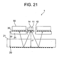
- FIG. 21 shows an example of a structure disclosed in Japanese Patent Application Laid-open Publication No. 2003-166856 .
- the documents WO 01/86232 and EP 0 672 891 also disclose such optical encoders.
- the detecting head includes a light source 14 in which a first grating 11 is disposed, and a photodetector 50 in which a third grating 30 is disposed.
- a second grating 20 is formed on a scale 21.
- self image means an optical pattern having a shape substantially similar to the second grating 20 formed on the light receiving surface of the photodetector 50. Moreover, the self image moves according to a relative displacement of the detecting head and the scale 21. The photodetector 50 detects the movement of the self image.
- Such type hereinafter, will be called as a "reflecting triple grating type”.
- the first grating and the third grating included in the detecting head are disposed by lining up the heights thereof.
- the self image can be classified into the following two typical cases (a) and (b) for example, according to structural conditions of the optical encoder, where case (a) is a case of having a same space period as of a shadow pattern of the second grating, and case (b) is a case of having the space period 1/2, 1/4, and ... of the shadow pattern of the second grating.
- Inventors of this patent application performed the following experiment, and calculated a tolerance of ⁇ zd required for achieving satisfactory signal strength by the photodetector. According to results of the experiment, it was revealed that, with predetermined conditions, to achieve the satisfactory signal amplitude at the photodetector, such as signal strength at which the maximum signal amplitude is 1/2 for example, the tolerance of ⁇ zd is ⁇ 36 ⁇ m. Moreover, it was revealed that with other conditions, for achieving the satisfactory signal strength at the photodetector, the tolerance of ⁇ zd is approximately ⁇ 33 ⁇ m.
- the tolerance of machining accuracy is in a range of ⁇ 50 ⁇ m to ⁇ 100 ⁇ m. Therefore, from a point of view of manufacturing, it is extremely difficult to dispose by mounting the first grating, the second grating, and the third grating such that the ⁇ zd is in a range of ⁇ 36 ⁇ m to ⁇ 33 ⁇ m. Moreover, when an attempt is made to realize an optical encoder in which ⁇ zd is not greater than the range of ⁇ 36 ⁇ m to ⁇ 33 ⁇ m, a dimensional tolerance of structure members of the optical encoder being small, it becomes very difficult to manufacture at a low cost. Moreover, in the conventional example described above, a concrete method or a structure which is assembled with the tolerance ⁇ zd to be very small is not at all disclosed.
- the present invention is made in view of the aforementioned problems, and an object of the present invention is to realize a tolerance which makes the manufacturing easy by relaxing a tolerance of ⁇ zd mentioned above, and to provide a triple grating type optical encoder which can be mass produced at a low cost.
- the light projecting section is structured to irradiate the predetermined light by combining a light source and a first grating which is disposed on a side facing the scale with respect to the light source, and an optical grating of a first pitch is formed in the first grating with respect to a direction of the relative displacement.
- the photodetecting section is structured to detect the movement of the self image by combining the photodetector and a third grating which is disposed on the light receiving surface of the photodetector, and an optical grating of a third pitch is formed in the third grating for the direction of the relative displacement.
- Each of a formation surface of the first grating and a formation surface of the third grating is disposed substantially parallel with respect to the scale, and in an optical path of light emitting from the light projecting section and reaching up to the photodetecting section upon being reflected and diffracted by the scale, a light transmitting area which is substantially flat and substantially parallel to the scale is formed on a surface of the detecting head facing the scale.
- a light transparent member which has a refractive index greater than 1 is disposed in a space between the surface of the detecting head and the first grating, and in a space between the surface of the detecting head and the third grating.
- the first grating includes an optical grating formed on a light transparent substrate, and the light projecting section is structured by attaching the light transparent substrate to a light emitting surface of the light source.
- the first grating is an optical grating formed directly on the light emitting surface of the light source, or an electrode pattern in the form of a grating which also serves as an electric current injecting electrode of the light source.
- the light source is a bare chip or a surface emitting semiconductor device in which the bare chip is seal-molded.
- At least one of the first grating and the third grating is an optical grating formed in the light transparent substrate, and a side surface of the light transparent substrate is covered by a light transparent resin.
- a light transparent member in the form of a plate disposed parallel to the scale is disposed on a side facing the scale with respect to the first grating and the third grating, and the light transparent substrate or a light transparent resin is disposed in a space between the light transparent member in the form of a plate and the first grating, and in a space between the light transparent member in the form of a plate and the third grating.
- an optical encoder which includes a scale which is installed on one of members of which a displacement is detected, and a detecting head which is installed on other member which is displaced relatively with respect to the one of the members, and which is disposed facing the scale, where the scale is provided with a second grating which has an optical pattern of a second pitch with respect to the direction of the relative displacement, and the detecting head is provided with a light projecting section which irradiates a predetermined light on the scale, and a photodetecting section which detects a movement of a self image which is formed on a light receiving surface of a photodetector by light which is irradiated from the light projecting section to the scale, and which is reflected and diffracted by the second grating.
- the light projecting section is structured to irradiate the predetermined light by combining a light source and a first grating which is disposed on a side facing the scale with respect to the light source, and an optical grating of a first pitch is formed in the first grating with respect to the direction of the relative displacement.
- the photodetecting section is structured to detect the movement of the self image by a photodetector and at least one light receiving element array disposed on the photodetecting section.
- the light receiving element array includes light receiving elements having a pitch of substantial integral multiples of a periodic intensity distribution of the self image, and each light receiving element in the light receiving element array is disposed by shifting through a fixed dimension in the direction of relative displacement, and the light receiving surface and the formation surface of the first grating are disposed substantially parallel with respect to the scale, and in an optical path of light emitting from the light projecting section and reaching up to the photodetecting section upon being reflected and diffracted by the scale, the light transmitting area which is substantially flat and substantially parallel to the scale is formed on the surface of the detecting head facing the scale.
- the light transparent member which has a refractive index greater than 1 is disposed in the space between the surface of the detecting head and the first grating, and in the space between the surface of the detecting head and the light receiving element array.
- the first grating includes an optical grating formed on a light transparent substrate, and the light projecting section is structured by attaching the light transparent substrate to the light emitting surface of the light source.
- the first grating is an optical grating formed directly on the light emitting surface of the light source, or an electrode pattern in the form of a grating which also serves as the electric current injecting electrode of the light source.
- the light source is a bare chip or a surface emitting semiconductor device in which the bare chip is seal-molded.
- the first grating is an optical grating formed in the light transparent substrate, and the side surface of the light transparent substrate is covered by a light transparent resin.
- At least the space from the first grating up to the surface of the detecting head, and the space from the light receiving element array up to the surface of the detecting head are sealed by a light transparent resin.
- the light transparent member in the form of a plate disposed parallel to the scale is disposed on a side facing the scale with respect to the first grating and the light receiving surface, and the light transparent substrate or a light transparent resin is disposed in the space between the light transparent member in the form of a plate and the first grating, and in a space between the light transparent member in the form of a plate and the light receiving surface.
- the light transparent member, a light transparent substrate, and a light transparent resin have a predetermined optical transmittance with respect to a predetermined wavelength region in which a light from the light source is emerged, and the optical transmittance is not greater than 1/2 with respect to at least one of a light of a wavelength side longer than the predetermined wavelength region, and a light of a wavelength side shorter than the predetermined wavelength region.
- a refractive index of the light transparent member is not less than 1.4 in a central wavelength of light emerged from the light source.
- Fig. 1 is a perspective view of a structure an optical encoder 100 according to a first embodiment of the present invention.
- Fig. 2 is a cross-sectional view of the structure of the optical encoder 100 according to the first embodiment.
- the structure of the optical encoder 100 will be described. Further, an experiment related to a tolerance carried out by inventors of the present patent application will be described. Based on a result of the experiment, an action effect of the first embodiment will be described.
- a scale 121 having a flat and parallel form is disposed as one of members detecting a displacement.
- a second grating 120 is formed on a surface of the scale 121 towards a detecting head.
- the second grating 120 is an optical pattern formed by a second pitch p2 with respect to a direction along y axis in Fig. 1 and Fig. 2 for example, which is a direction of relative displacement of the scale 121 and a substrate 160 which will be described later.
- a bare chip LED 141 and a light transparent substrate 111 are stacked on the substrate 160.
- the substrate 160 corresponds to other member which is displaced relatively with respect to the scale 121.
- the bare chip LED 141 corresponds to a light source.
- a first grating 110 is formed on a surface of the light transparent substrate 111 on a side of the bare chip LED 141.
- the first grating 110 is an optical pattern formed by a first pitch p1 with respect to the direction along y axis in which the scale 121 and the substrate 160 are displaced relatively.
- a combination of the bare chip LED 141 and the first grating 110 corresponds to a light projecting section.
- a photodetector 150 and a light transparent substrate 131 are stacked on the substrate 160.
- a third grating 130 is formed on a surface of the light transparent substrate 131 on a side of the photodetector 150.
- the third grating 130 is an optical pattern formed by a third pitch p3 with respect to the direction along y axis in which the scale 121 and the substrate 160 are displaced relatively.
- a combination of the photodetector 150 and the third grating 130 corresponds to the photodetecting section. Further, a structure in which the projecting section and the photodetecting section are combined corresponds to the detecting head.
- the photodetecting section which includes the photodetector 150 and the third grating 130 detects a movement of a self image which is formed on a light receiving surface of the photodetector 150 by light which is irradiated from the light projecting section to the scale 121, and which is reflected and diffracted by the second grating 120.
- the bare chip LED 141, the light transparent substrate 111, the photodetector 150, and the light transparent substrate 131 which are disposed on the substrate 160 are embedded to be covered by a light transparent resin 190.
- Each of a formation surface of the first grating 110 and a formation surface of the third grating 130, is disposedparallel with respect to the scale 121.
- a light transmitting area which is substantially flat and substantially parallel to the scale 121 is formed on a surface of the detecting head facing the scale 121.
- a surface of the light transparent resin 190 on a side of the scale 121 is formed to be substantially flat and substantially parallel with respect to the scale 121.
- the scale 121 on which the second grating 120 is formed is disposed parallel to the first grating 110 and the third grating 130 such that the scale 121 is capable of a relative displacement in y direction.
- a plane parallel to the formation surface of the first grating 110, the formation surface of the second grating 120, and the formation surface of the third grating 130 is let to be xy plane.
- y direction is let to be a grating pitch direction of the second grating 120
- x direction is let to be a direction perpendicular to the grating pitch direction of the second grating 120
- z direction is let to be a direction perpendicular to the xy plane.
- An electrode pad 170 is formed on an upper surface of the bare chip LED 141.
- the electrode pad 170 on the bare chip LED 141 is connected to another electrode pad 170 on the substrate 160 via an electroconductive wire 171. Electrical wiring of the light source and the photodetector is omitted in Fig. 1 and Fig. 2 .
- each of structural parameters ⁇ , z1, z2, p1, p2, and p3 may be set in advance based on equations (1) to (8).
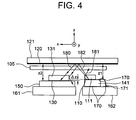
- the inventors of the present invention carried out an experiment about a relation of ⁇ zd and the signal amplitude from the photodetector 150 for a structure in Fig. 3 and Fig. 4 , to find the tolerance of ⁇ zd for a reflecting triple grating type optical encoder.
- the bare chip LED 141 and the light transparent substrate 111 on which the first grating 110 is formed are stacked on a substrate 161.
- the photodetector 150 and the light transparent substrate 131 on which the third grating 130 is formed are stacked on a substrate 162 which is a substrate apart from the substrate 161.
- the scale 121 on which the second grating 120 is formed is disposed parallel to the formation surface of the first grating 110 and the formation surface of the third grating 130.
- the plane parallel to each of the formation surfaces of the first grating 110, the second grating 120, and the third grating 130 is let to be xy plane.
- y direction is let to be the grating pitch direction of the second grating 120
- x direction is let to be the direction perpendicular to the grating pitch direction of the second grating 120
- z direction is let to be the direction perpendicular to the xy plane.
- a light transmission plate 105 shown in Fig. 3 is to be neglected in the description of this experiment.
- a horizontal axis in Fig. 5 denotes ⁇ zd (unit: mm), and a vertical axis denotes the signal amplitude (unit: arbitrary, normalized with the maximum value).
- ⁇ 650 nm
- p2 20 ⁇ m
- n 1.
- the first grating 110, the second grating 120, and the third grating 130 are required to be disposed by mounting such that ⁇ zd is not greater than ⁇ 36 ⁇ m to ⁇ 33 ⁇ m.
- the first grating 110, the second grating 120, and the third grating 130 are required to be disposed by mounting such that ⁇ zd is not greater than ⁇ 36 ⁇ m to ⁇ 33 ⁇ m.
- a normal tolerance of machining accuracy is in a range of about ⁇ 50 ⁇ m to ⁇ 100 ⁇ m. Therefore, from a manufacturing point of view, it is extremely difficult to dispose by mounting the first grating 110, the second grating 120, and the third grating 130 such that ⁇ zd is not greater than ⁇ 36 ⁇ m to ⁇ 33 ⁇ m.
- curve L2 in Fig. 5 denoted by alternate long and short dash line
- the tolerance of ⁇ zd for which the signal amplitude is 1/2 is approximately ⁇ 62 ⁇ m. It is revealed that the tolerance is relaxed (becomes large) by approximately 1. 7 times as compared to a case in air mentioned above (curve L1 in Fig. 5 ).
- the refractive index of the light transmission plate 105 is let to be nindex, and the refractive index in the air is let to be 1, when the light transmission plate 105 is there, it was observed that the value of z1 and z2 at which the maximum wavelength can be achieved is increased by t ⁇ (nindex - 1) as compared to when the light transmission plate 105 is not there.
- a distance between the surface of the detecting head on the light projecting section and the formation surface of the second grating 120 is let to be z10 and the distance between a surface of the detecting head on the photodetecting section and the formation surface of the second grating 120 is let to be z20.
- a light transmitting area which is substantially flat and substantially parallel to the scale 121 is formed on the surface of the detecting head facing the scale 121.
- ⁇ zd mentioned above is determined by the following two factors (a) and (b).
- a normal light transparent member has a refractive index not less than 1, glass has a refractive index of about 1.5 and a light transparent resin has a refractive index of about 1.4 to 2 for example. Therefore, when the glass or the light transparent resin is used, the tolerance of the heights of the first grating 110 and the third grating 130 is relaxed by about 1. 4 to 2 times. This is a reason for the tolerance of ⁇ zd relaxed when the entire detecting head is filled with the light transparent resin 190 and sealed. Moreover, it is desirable that the refractive index of the light transparent member is not less than 1.4 in the central wavelength of light emerged from the light source. It is desirable for all embodiments that the refractive index of the light transparent member is not less than 1.4.
- the light transmitting area which is substantially flat and substantially parallel to the scale 121 is formed on the surface of the detecting head facing the scale 121.
- the light transparent resin 190 which is a light transparent member is disposed in the space between the surface of the detecting head and the first grating 110, and in the space between the surface of the detecting head and the third grating 130. Therefore, a dimensional tolerance and a mounting tolerance of the structure member are relaxed (becomes large). As a result of this, the optical encoder 100 can be mass produced at a low cost.
- a required accuracy of the tolerance ⁇ zd is relaxed.
- Light emerged from the bare chip LED 141 is irradiated on the second grating 120 on the scale 121 via the light transparent substrate 111 on which the first grating 110 is formed.
- Light reflected and diffracted at the second grating 120 is reached to the photodetector 150 via the light transparent substrate 131 on which the third grating 130 is formed.
- Each member disposed on the substrate 160 is embedded in the light transparent resin 190. Therefore, there is an advantage that a tolerance of a height difference between the first grating 110 and the third grating 130 is increased by the portion of the refractive index of the light transparent resin 190.
- the reason for the light reflection being suppressed at the side surface of the light transparent substrate 111 and 131, is that a difference between the refractive index of the light transparent substrates 111 and 131, and the refractive index of the light transparent resin 190 is smaller than a difference between the refractive index of the light transparent substrate 111 and 131, and the refractive index of air.
- the critical angle of total internal reflection is determined by a difference in refractive index of the light transparent substrates 111 and 131, and a refractive index of a member in contact with the light transparent substrates 111 and 113, and smaller the difference in the refractive indices, the angle of total internal reflection increases, and the total internal reflection does not occur.
- the manufacturing of the light projecting section becomes easy.
- the bare chip LED 141 as the light source, the light projecting section can be manufactured to be thin and at a low cost.
- each component member of the first embodiment can be transformed and modified into various types.
- the bare chip LED is used as the light source.
- the light source is not restricted to the bare chip LED, and may be any one such as a normal LED molded component and a surface emitting laser, which can form a self image.
- the third grating 130 is a group of gratings was described.
- the third grating 130 also includes a structure in which a plurality of grating group is disposed by shifting phases thereof, and a photodetector is disposed for each of the grating.
- a structure in which the second grating 120, the first grating 110, and the third grating 130 on the scale 121 are at a constant period, and a structure in which an amount of relative displacement is detected was described.
- an optical pattern for detecting a reference position can also be disposed near each of the first grating 110, the second grating 120, and the third grating 130.
- a one-dimensional grating pattern of the first grating 110, the second grating 120, and the third grating 130 is described.
- a structure in which the gratings are formed in a two-dimensional form, and a two-dimensional displacement is detected is also possible.
- the surface on which the first grating 110 is formed on the light transparent substrate 111 is let to be a surface facing the bare chip LED 141.
- the surface on which the third grating 130 is formed on the light transparent substrate 131 is let to be a case of a surface facing the photodetector 150.
- the present invention is not restricted to this, and the first grating 110 and the third grating 130 formed on the light transparent substrate 111 and the light transparent substrate 131 respectively, may be formed on a surface facing the scale 121.
- any method can be used for covering a surrounding of the detecting head by the light transparent resin 190.
- methods such as a method of dispensing the light transparent resin 190 corresponding to each detecting head, a method of applying a light transparent resin on an entire surface of a large size after mounting component members of several detecting heads on the large size substrate, and after curing (hardening) the resin, and isolating into individual detecting head by dicing, are available.
- any method such as a resin mold method, a method of making the surface substantially flat by a surface tension, and a method of polishing after coating can be applied.
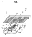
- Fig. 6 is a perspective view of a structure of an optical encoder 200 according to a second embodiment of the present invention.
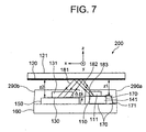
- Fig. 7 is a cross-sectional view of the structure of the optical encoder 200 according to the second embodiment of the present invention.
- the second embodiment differs from the first embodiment at points that in the second embodiment, each of the projecting section in which the bare chip LED 141 and the first grating 110 are stacked, and the photodetecting section in which the photodetector 150 and the third grating 130 are stacked, is covered by a light transparent resin 290a and a light transparent resin 290b which are different.
- the same reference numerals are used for components which are same as in the first embodiment and their description is omitted to avoid repetition.
- the light transparent resin 290a covers an optical path from the bare chip LED 141 up to the scale 121.
- the light transparent resin 290b covers an optical path from the scale 121 up to the photodetector 150.
- light transparent resin 290a and the light transparent resin 290b may be ensured to have flatness only in an area through which the respective light passes.
- each of the side surfaces of the light transparent substrates 111 and 131 is covered by the light transparent resin 290a and the light transparent resin 290b respectively. Accordingly, a surface in contact with the air is away from a light emitting portion of the bare chip LED 141. As a result of this, an effect in which, the total internal reflection of light emerged from the bare chip LED 141 at the side surface of the light transparent substrates 111 and 131 can be reduced, is shown. Actions other than this are similar to actions in the first embodiment. Moreover, each structure of the second embodiment can be transformed and modified into various types of structures similarly as in the first embodiment.
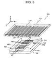
- Fig. 8 shows a perspective view of a structure of an optical encoder 300 according to a third embodiment of the present invention.
- Fig. 9 shows a cross-sectional view of the structure of the optical encoder 300 according to the third embodiment.
- the third embodiment differs from the first embodiment at a point that in the third embodiment, a plurality of periodic rectangular openings (apertures) of the first pitch (period) p1 described above is formed on an electrode 143 in the form of a grating on the upper surface of the bare chip LED 141.
- the same reference numerals are used for components same as in the first embodiment, and the description is omitted to avoid repetition.
- the periodic openings (apertures) of the electrode 143 in the form of a grating of the bare chip LED 141 show a function similar to a function of the first grating 110.
- this structure in addition to the effect of the first embodiment, there is an advantage that a process of stacking the bare chip LED 141 and the first grating 110 can be omitted, thereby making the manufacturing easy.
- the light projecting section can be structured to be thin.
- Each structure of the third embodiment can be transformed and modified into various types of structures similarly as in the first embodiment.
- Fig. 10 shows a perspective view of a structure of an optical encoder 400 according to a fourth embodiment of the present invention.
- Fig. 12 shows a cross-sectional view of the structure of the optical encoder 400 according to the fourth embodiment.
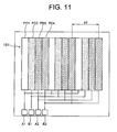
- the fourth embodiment differs from the first embodiment at a point that in the fourth embodiment, the photodetector is let to be a light receiving element array formed with the third pitch (period) p3 as shown in Fig. 11 .
- the same reference numerals are used for components same as in the first embodiment, and the description of these components is omitted to avoid repetition.
- Fig. 11 shows an enlarged view of a light receiving element array 151 formed on the photodetector 150.
- the light receiving element array 151 includes a plurality of sets of four photodiodes PD1, PD2, PD3, and PD4 having a rectangular shape, combined together.
- the photodiodes PD1, PD2, PD3, and PD4 are disposed in the form of comb teeth, each shifted through 1/4 ⁇ p3. Moreover, an electric signal from each of the photodiodes PD1, PD2, PD3, and PD4 is output from four electrode pads A1, B1, A2, and B2.
- the plurality of photodiodes PD1, PD2, PD3, and PD4 having a different phase can be disposed at substantially the same position. Therefore, it is possible to relax significantly a rotational tolerance in the plane as compared to a case in which the plurality of sets of the third grating 130 and the photodetector 150 is positioned at different positions. Furthermore, the light transparent substrate on which the third grating 130 is formed is not required to be mounted. Therefore, in the fourth embodiment, a function of the third grating 130 can be realized easily with high accuracy and at further lower cost.
- the pitch of the photodiodes PD1, PD2, PD3, and PD4 may also be in integral multiples of P3. Moreover, amount through which each of the photodiodes PD1, PD2, PD3, and PD4 is shifted (shifting amount) is not restricted to 1/4 ⁇ p3, and various configurations such as three sets having the shifting amount 1/3 ⁇ p3 (three sets of photodiodes), four sets having the shifting amount 3/4 ⁇ p3 (four sets of photodiodes), and m sets having the shifting amount 1/m ⁇ p3 (where m is a natural number, and m sets of photodiodes).
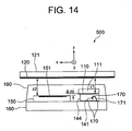
- Fig. 13 shows a perspective view of a structure of an optical encoder 500 according to a fifth embodiment of the present invention.
- Fig. 14 shows a cross-sectional view of the structure of the optical encoder 500 according to the fifth embodiment.
- a resin mold LED 144 is used as the light source of the light projecting section.
- the electrode pad 170 on the upper surface of the bare chip LED 141 is connected to the electrode pad 171 on a lower surface of the resin mold LED 144 by the electroconductive wire 171.
- the other electrode pad 170 of the bare chip LED 141 is connected directly to the electrode pad 170 on a lower surface of the resin mold LED 144 by a material such as a solder material.
- the light transparent substrate 111 on which the first grating 110 is formed is stacked on an upper surface of the resin mold LED 144. The rest of the structure is similar to the structure in the fourth embodiment.
- the basic action of the fifth embodiment is similar to the basic action of the fourth embodiment.
- the resin mold LED 144 By replacing the bare chip LED by the resin mold LED 144, there is some increase in a thickness and planar dimensions of the light projecting section. However, a size of the substrate on which the first grating 110 is formed is increased, thereby easing the handling, and a bonding pad of the conductive wire disposed on the upper surface of the bare chip LED is not required. Accordingly, there is an advantage that the mounting of the light transparent substrate 111 on which the resin mold LED 144 and the first grating 110 are formed becomes easy.
- a tolerance for variation in a height of the resin mold LED 144 is about ⁇ 60 ⁇ m.
- the tolerance for variation in the height of the resin mold LED 144 can be reduced to 1/nindex.
- the tolerance for the variation in the height of the resin mold LED 144 is equal to about ⁇ 30 ⁇ m which is a value when disposed in the air. Therefore, even when the resin mold LED 144 having the tolerance for variation in the height ⁇ 60 ⁇ m is used, it is possible to realize a range of tolerance of the experiment result mentioned above.
- each structure of the fifth embodiment can be transformed and modified to various structures.
- the upper surface of the resin mold LED 144 is not required to be flat entirely, and a joining portion of the light transparent substrate 111 on which the first grating 110 is formed may be let to be flat.
- a concavity and convexity having a function of a lens may be formed on a portion other than the flat area on the surface of the resin mold LED 144. Accordingly, it is also possible to control an angle of irradiation of the light beam such that the light beam is guided effectively to the photodetector 150.
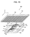
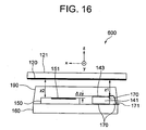
- Fig. 15 shows a perspective view of a structure of an optical encoder 600 according to a sixth embodiment of the present invention.
- Fig.16 shows a cross-sectional view of the structure of the optical encoder 600 according to the present invention.
- the structure of the light projecting section is formed identically as in the third embodiment, and the photodetecting section is formed identically as in the fourth embodiment.
- An action of the light projecting section is the same as an action of the light projecting section in the third embodiment.
- an action of the photodetecting section is same as an action of the photodetecting section in the fourth embodiment. Therefore, the light transparent substrates 111 and 131 on which the first grating 110 and the third grating 130 are formed are not required to be mounted. Accordingly, it is possible to realize a function of the first grating 110 and the third grating 130 with high accuracy and at low cost.
- Each structure of the sixth embodiment can be transformed and modified into various types of structures. Examples of transformation are similar as in the third embodiment and in the fourth embodiment.
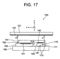
- Fig. 17 shows a cross-sectional view of a structure of an optical encoder 700 according to a seventh embodiment of the present invention.
- a light transparent substrate 791 on which a first grating 143 is formed is stacked on the upper surface of the resin mold LED 144, and the light receiving element array 151 is used in the photodetecting section.
- a light transparent member 791 in the form of a plate is disposed on an upper portion of the light projecting section and the photodetecting section, such that the light transparent member 791 faces in parallel with a surface of the scale 121.
- a light transparent resin 790 is disposed in a gap developed by a difference in a height of the light projecting section and a height of the photodetecting section.
- the light transparent resin 790 may be allowed to have a function of an adhesive.
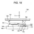
- Fig. 18 shows a cross-sectional view of a structure of an optical encoder 750 according to a modified embodiment of the seventh embodiment.
- Fig. 17 is an example of a structure in which the light transparent resin 790 is disposed between the light receiving element array 151 (third grating) and the light transparent member 791 in the form of a plate.
- the modified embodiment of the seventh embodiment is an example in which, the light transparent resin 790 is disposed between the electrode 143 in the form of a grating (first grating) and the light transparent member 791 in the form of a plate.
- the rest of the structure is similar to the structure in the first embodiment.
- the light transparent resin 790 is disposed between the electrode 143 in the form of a grating (first grating) and the light transparent member 791 in the form of a plate, or between the light receiving element array 151 (third grating) and the light transparent member 791 in the form of a plate. Therefore, it is possible to have a substantial tolerance of height of disposing of the electrode 143 in the form of a grating (first grating) and the light receiving element array 151 (third grating).
- Each structure of the modified embodiment of the seventh embodiment can be transformed and modified into various types of structures.
- Space to be embedded (filled) by the light transparent resin 791 need not necessarily be restricted to the gap between the electrode 143 in the form of a grating (first grating), the light receiving element array 151 (third grating), and the light projecting section and the photodetecting section.
- a structure in which a side surface of the light projecting section and the photodetecting section are embedded may also be used.
- Other modified embodiments are similar to the fifth embodiment and the sixth embodiment for example.
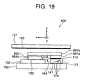
- Fig. 19 shows a cross-sectional view of a structure of an optical encoder 800 according to an eighth embodiment of the present invention.
- the eighth embodiment is similar to the first embodiment except for the structure of the light projecting section and the photodetecting section, in which the resin mold LED is used instead of the bare chip LED.
- light transparent members 891a, 891b, and 891c in the form of a plate are disposed on the upper portion of the light projecting section and the photodetector 150, such that the light transparent members face in parallel with the surface of the scale 121.
- a light transparent resin 890 is disposed in the gap developed by a difference in the height of the light projecting section and the height of the photodetector 150.
- the light transparent resin 890 may be allowed to have the function of an adhesive.
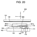
- Fig. 20 shows a cross-sectional view of a structure of an optical encoder 850 according to a modified embodiment of the eighth embodiment.
- light transparent members 991a, 991b, and 991c in the form of a plate are disposed.
- the modified embodiment of the eighth embodiment is an example of a structure in which a light transparent resin 990 is disposed between the first grating 110 and the light transparent member 991b in the form of a plate. The rest of the structure is similar to the structure in the first embodiment.
- the light transparent resins 890 and 990 are disposed between the first grating 110 and the light transparent member 991b in the form of a plate, or between the third grating 130 and the light transparent member 891b in the form of a plate. Therefore, it is possible to have a substantial tolerance of height of disposing the first grating 110 and the third grating 130.
- Each structure of the modified embodiment of the eighth embodiment can be transformed and modified into various types of structures.
- Space to be embedded (filled) by the light transparent resins 890 and 990 need not necessarily be restricted to the gap between the first grating 110, the second grating 130, and the light projecting section and the photodetector.
- a structure in which the side surface of the light projecting section and the photodetecting section are embedded may also be used.
- Other modified embodiments are similar to the first embodiment for example.
- the structure can be let to be the following structures (1), (2), and (3).
- the light transparent member and the light transparent resin may be let to be a member and a resin which have the optical transparency for the wavelength of the light source, and may not be let to have the optical transparency for a wavelength other than the wavelength of the light source.
- the wavelength of the light source is set in the region of the ultraviolet light or the visible light for example
- the light transparent member, the light transparent substrate, and the light transparent resin have the optical transparency for the wavelength of the light source, but may be let to have a less optical transmittance for the infra-red light. Accordingly, in an environment of substantial infra-red light, sensing in which an effect due to the infra-red light is suppressed is possible.
- the light transparent member, the light transparent substrate, and the light transparent resin have the optical transparency for the wavelength of the light source, but may be let to have a less optical transmittance for the visible light. Accordingly, in an environment of substantial visible light, a sensing in which an effect due to the visible light is suppressed is possible.
- the light transparent member, the light transparent substrate, and the light transparent resin have the optical transparency for the wavelength of the light source, but may be let to have a less optical transmittance for the ultraviolet light. Accordingly, in an environment of substantial ultraviolet light, a sensing in which an effect due to the ultraviolet light is suppressed is possible.
- an optical encoder is a reflecting triple grating type encoder.
- Alight transparent member is disposed in a space between a surface of a detecting head and a first grating, and in a space between the surface of the detecting head and a third grating. Accordingly, it is possible to relax a tolerance of ⁇ zd corresponding to a refractive index of the light transparent member. As a result of this, it is possible to realize a tolerance which makes the manufacturing easy, and to provide a triple grating type optical encoder which can be mass produced at a low cost.
- optical encoder according to the present invention is useful for the reflecting triple grating type optical encoder in which the tolerance between the structure members is relaxed.
Description
- The present invention relates to a reflecting triple grating type optical encoder which detects a position of an obj ect to be detected.
- An optical encoder which includes a detecting head and a scale are hitherto known (refer to Japanese Patent Application Laid-open Publication No.
2003-166856 Fig. 21 shows an example of a structure disclosed in Japanese Patent Application Laid-open Publication No.2003-166856 WO 01/86232 EP 0 672 891light source 14 in which afirst grating 11 is disposed, and aphotodetector 50 in which athird grating 30 is disposed. Moreover, a second grating 20 is formed on ascale 21. Light emerged from thelight source 14 forms a self image on a light receiving surface of thephotodetector 50 upon being affected by thefirst grating 11 and thesecond grating 20. In this patent application, "self image" means an optical pattern having a shape substantially similar to thesecond grating 20 formed on the light receiving surface of thephotodetector 50. Moreover, the self image moves according to a relative displacement of the detecting head and thescale 21. Thephotodetector 50 detects the movement of the self image. Such type, hereinafter, will be called as a "reflecting triple grating type". - In the reflecting triple grating type optical encoder, it is desirable to perform a detection which is not affected easily by a change in a distance between the scale and the detecting head. For this, the first grating and the third grating included in the detecting head are disposed by lining up the heights thereof. Moreover, the self image can be classified into the following two typical cases (a) and (b) for example, according to structural conditions of the optical encoder, where case (a) is a case of having a same space period as of a shadow pattern of the second grating, and case (b) is a case of having the
space period 1/2, 1/4, and ... of the shadow pattern of the second grating. - The most stable and the clearest image is formed in the case (a) mentioned above. Therefore, the case (a) mentioned above will be described below.
- When the following conditional equation (1) is satisfied, a self image having the same space period as of the shadow pattern of the second grating is observed on the light receiving surface of the photodetector.

where,
λ denotes a central wavelength of light emitted from the light source,
z1 denotes an optical distance between the first grating and the second grating,
z2 denotes an optical distance between the second grating and the third grating,
p2 denotes a pitch of the second grating, and
k denotes a natural number. - Here, when
Δ z0 is let to be a difference between z2 and z1, which is designed in advance,
Δ z is let to be a difference between z2 and z1 when actually manufactured, and
Δ zd is let to be a difference between Δz0 and Δz which occurred when actually manufactured (in other words, a difference between
Δ z0 designed in advance and Δz when actually prepared) the following equation (2) holds.
- Inventors of this patent application performed the following experiment, and calculated a tolerance of Δzd required for achieving satisfactory signal strength by the photodetector. According to results of the experiment, it was revealed that, with predetermined conditions, to achieve the satisfactory signal amplitude at the photodetector, such as signal strength at which the maximum signal amplitude is 1/2 for example, the tolerance of Δzd is ±36 µm. Moreover, it was revealed that with other conditions, for achieving the satisfactory signal strength at the photodetector, the tolerance of Δzd is approximately ±33 µm.
- Generally, the tolerance of machining accuracy is in a range of ±50 µm to ±100 µm. Therefore, from a point of view of manufacturing, it is extremely difficult to dispose by mounting the first grating, the second grating, and the third grating such that the Δzd is in a range of ±36 µm to ±33 µm. Moreover, when an attempt is made to realize an optical encoder in which Δzd is not greater than the range of ±36 µm to ±33 µm, a dimensional tolerance of structure members of the optical encoder being small, it becomes very difficult to manufacture at a low cost. Moreover, in the conventional example described above, a concrete method or a structure which is assembled with the tolerance Δzd to be very small is not at all disclosed.
- The present invention is made in view of the aforementioned problems, and an object of the present invention is to realize a tolerance which makes the manufacturing easy by relaxing a tolerance of Δzd mentioned above, and to provide a triple grating type optical encoder which can be mass produced at a low cost.
- To find a solution to the aforementioned issues, and to achieve the object, there can be provided an optical encoder according to
claim 1. - In this optical encoder, the light projecting section is structured to irradiate the predetermined light by combining a light source and a first grating which is disposed on a side facing the scale with respect to the light source, and
an optical grating of a first pitch is formed in the first grating with respect to a direction of the relative displacement. - The photodetecting section is structured to detect the movement of the self image by combining the photodetector and a third grating which is disposed on the light receiving surface of the photodetector, and
an optical grating of a third pitch is formed in the third grating for the direction of the relative displacement. - Each of a formation surface of the first grating and a formation surface of the third grating is disposed substantially parallel with respect to the scale, and
in an optical path of light emitting from the light projecting section and reaching up to the photodetecting section upon being reflected and diffracted by the scale, a light transmitting area which is substantially flat and substantially parallel to the scale is formed on a surface of the detecting head facing the scale. - A light transparent member which has a refractive index greater than 1 is disposed in a space between the surface of the detecting head and the first grating, and in a space between the surface of the detecting head and the third grating.
- Moreover according to a preferable aspect of the present invention, it is desirable that
the first grating includes an optical grating formed on a light transparent substrate, and
the light projecting section is structured by attaching the light transparent substrate to a light emitting surface of the light source. - Moreover according to another preferable aspect of the present invention, it is desirable that
the first grating is an optical grating formed directly on the light emitting surface of the light source, or an electrode pattern in the form of a grating which also serves as an electric current injecting electrode of the light source. - Furthermore, according to still another preferable aspect of the present invention, it is desirable that
the light source is a bare chip or a surface emitting semiconductor device in which the bare chip is seal-molded. - According to still another preferable aspect of the present invention, it is desirable that
at least one of the first grating and the third grating is an optical grating formed in the light transparent substrate, and
a side surface of the light transparent substrate is covered by a light transparent resin. - Moreover, according to still another preferable aspect of the present invention, it is desirable that
at least a space from the first grating and the third grating up to the surface of the detecting head is sealed by the light transparent resin. - Furthermore, according to still another aspect of the present invention, it is desirable that
a light transparent member in the form of a plate disposed parallel to the scale is disposed on a side facing the scale with respect to the first grating and the third grating, and
the light transparent substrate or a light transparent resin is disposed in a space between the light transparent member in the form of a plate and the first grating, and in a space between the light transparent member in the form of a plate and the third grating. - According to the present invention, there can be provided an optical encoder which includes
a scale which is installed on one of members of which a displacement is detected, and
a detecting head which is installed on other member which is displaced relatively with respect to the one of the members, and which is disposed facing the scale, where
the scale is provided with a second grating which has an optical pattern of a second pitch with respect to the direction of the relative displacement, and
the detecting head is provided with a light projecting section which irradiates a predetermined light on the scale, and
a photodetecting section which detects a movement of a self image which is formed on a light receiving surface of a photodetector by light which is irradiated from the light projecting section to the scale, and which is reflected and diffracted by the second grating. - In this optical encoder, the light projecting section is structured to irradiate the predetermined light by combining a light source and a first grating which is disposed on a side facing the scale with respect to the light source, and
an optical grating of a first pitch is formed in the first grating with respect to the direction of the relative displacement. - The photodetecting section is structured to detect the movement of the self image by a photodetector and at least one light receiving element array disposed on the photodetecting section.
- The light receiving element array includes light receiving elements having a pitch of substantial integral multiples of a periodic intensity distribution of the self image, and each light receiving element in the light receiving element array is disposed by shifting through a fixed dimension in the direction of relative displacement, and
the light receiving surface and the formation surface of the first grating are disposed substantially parallel with respect to the scale, and
in an optical path of light emitting from the light projecting section and reaching up to the photodetecting section upon being reflected and diffracted by the scale, the light transmitting area which is substantially flat and substantially parallel to the scale is formed on the surface of the detecting head facing the scale. - The light transparent member which has a refractive index greater than 1 is disposed in the space between the surface of the detecting head and the first grating, and in the space between the surface of the detecting head and the light receiving element array.
- Moreover, according to still another preferable aspect of the present invention, it is desirable that
the first grating includes an optical grating formed on a light transparent substrate, and
the light projecting section is structured by attaching the light transparent substrate to the light emitting surface of the light source. - Furthermore, according to still another preferable aspect of the present invention, it is desirable that the first grating is an optical grating formed directly on the light emitting surface of the light source, or an electrode pattern in the form of a grating which also serves as the electric current injecting electrode of the light source.
- According to still another preferable aspect of the present invention, it is desirable that
the light source is a bare chip or a surface emitting semiconductor device in which the bare chip is seal-molded. - Moreover, according to still another preferable aspect of the present invention, it is desirable that
the first grating is an optical grating formed in the light transparent substrate, and
the side surface of the light transparent substrate is covered by a light transparent resin. - Furthermore, according to still another preferable aspect of the present invention, it is desirable that
at least the space from the first grating up to the surface of the detecting head, and the space from the light receiving element array up to the surface of the detecting head are sealed by a light transparent resin. - According to still another preferable aspect of the present invention, it is desirable that the light transparent member in the form of a plate disposed parallel to the scale is disposed on a side facing the scale with respect to the first grating and the light receiving surface, and
the light transparent substrate or a light transparent resin is disposed in the space between the light transparent member in the form of a plate and the first grating, and in a space between the light transparent member in the form of a plate and the light receiving surface. - Moreover, according to still another preferable aspect of the present invention, it is desirable that the light transparent member, a light transparent substrate, and a light transparent resin have a predetermined optical transmittance with respect to a predetermined wavelength region in which a light from the light source is emerged, and the optical transmittance is not greater than 1/2 with respect to at least one of a light of a wavelength side longer than the predetermined wavelength region, and a light of a wavelength side shorter than the predetermined wavelength region.
- Furthermore, according to still another preferable aspect of the present invention, it is desirable that
a refractive index of the light transparent member is not less than 1.4 in a central wavelength of light emerged from the light source. -
-
Fig. 1 is a perspective view of a structure of an optical encoder according to a first embodiment of the present invention; -
Fig. 2 is a cross-sectional view of the structure of the optical encoder according to the first embodiment; -
Fig. 3 is a perspective view of a structure of an optical encoder used for an experiment; -
Fig. 4 is a cross-sectional view of the structure of the optical encoder used for the experiment; -
Fig. 5 is a diagram showing a result of the experiment; -
Fig. 6 is a perspective view of a structure of an optical encoder according to a second embodiment; -
Fig. 7 is a cross-sectional view of the structure of the optical encoder according to the second embodiment; -
Fig. 8 is a perspective view of a structure of an optical encoder according to a third embodiment; -
Fig. 9 is a cross-sectional view of the structure of the optical encoder according to the third embodiment; -
Fig. 10 is a perspective five of a structure of an optical encoder according to a fourth embodiment; -
Fig. 11 is a diagram showing a structure of a light receiving element array in the fourth embodiment; -
Fig. 12 is a cross-sectional view of the optical encoder according to the fourth embodiment; -
Fig. 13 is a perspective view of a structure of an optical encoder according to a fifth embodiment; -
Fig. 14 is a cross-sectional view of the structure of the optical encoder according to the fifth embodiment; -
Fig. 15 is a perspective view of a structure of an optical encoder according to a sixth embodiment; -
Fig. 16 is a cross-sectional view of the structure of the optical encoder according to the sixth embodiment; -
Fig. 17 is a cross-sectional view of a structure of an optical encoder according to a seventh embodiment; -
Fig. 18 is a cross-sectional view of a structure of an optical encoder according to a modified embodiment of the seventh embodiment; -
Fig. 19 is a cross-sectional view of a structure of an optical encoder according to an eighth embodiment; -
Fig. 20 is a cross-sectional view of a structure of an optical encoder according to a modified embodiment of the eighth embodiment; and -
Fig. 21 is a cross-sectional view of a structure of an optical encoder of a conventional technology. - Embodiments of an optical encoder according to the present invention will be described below in detail with reference to accompanying diagrams. However, the present invention is not restricted to the embodiments described below.
-
Fig. 1 is a perspective view of a structure anoptical encoder 100 according to a first embodiment of the present invention.Fig. 2 is a cross-sectional view of the structure of theoptical encoder 100 according to the first embodiment. Firstly, the structure of theoptical encoder 100 will be described. Further, an experiment related to a tolerance carried out by inventors of the present patent application will be described. Based on a result of the experiment, an action effect of the first embodiment will be described. - To start with, the structure of the
optical encoder 100 according to the first embodiment will be described. Ascale 121 having a flat and parallel form is disposed as one of members detecting a displacement. Asecond grating 120 is formed on a surface of thescale 121 towards a detecting head. Thesecond grating 120 is an optical pattern formed by a second pitch p2 with respect to a direction along y axis inFig. 1 andFig. 2 for example, which is a direction of relative displacement of thescale 121 and asubstrate 160 which will be described later. - Moreover, a
bare chip LED 141 and a lighttransparent substrate 111 are stacked on thesubstrate 160. Thesubstrate 160 corresponds to other member which is displaced relatively with respect to thescale 121. Thebare chip LED 141 corresponds to a light source. Afirst grating 110 is formed on a surface of the lighttransparent substrate 111 on a side of thebare chip LED 141. Thefirst grating 110 is an optical pattern formed by a first pitch p1 with respect to the direction along y axis in which thescale 121 and thesubstrate 160 are displaced relatively. A combination of thebare chip LED 141 and thefirst grating 110 corresponds to a light projecting section. Moreover, thebare chip LED 141 irradiates light of a wavelength λ = 650 nm for example. - A
photodetector 150 and a lighttransparent substrate 131 are stacked on thesubstrate 160. Athird grating 130 is formed on a surface of the lighttransparent substrate 131 on a side of thephotodetector 150. Thethird grating 130 is an optical pattern formed by a third pitch p3 with respect to the direction along y axis in which thescale 121 and thesubstrate 160 are displaced relatively. A combination of thephotodetector 150 and thethird grating 130 corresponds to the photodetecting section. Further, a structure in which the projecting section and the photodetecting section are combined corresponds to the detecting head. - The photodetecting section which includes the
photodetector 150 and thethird grating 130 detects a movement of a self image which is formed on a light receiving surface of thephotodetector 150 by light which is irradiated from the light projecting section to thescale 121, and which is reflected and diffracted by thesecond grating 120. - The
bare chip LED 141, the lighttransparent substrate 111, thephotodetector 150, and the lighttransparent substrate 131 which are disposed on thesubstrate 160 are embedded to be covered by a lighttransparent resin 190. - Each of a formation surface of the
first grating 110 and a formation surface of thethird grating 130, is disposedparallel with respect to thescale 121. Moreover, in an optical path of light emittign from the light projecting section and reaching up to the photodetecting section upon being reflected and diffracted, a light transmitting area which is substantially flat and substantially parallel to thescale 121 is formed on a surface of the detecting head facing thescale 121. In other words, a surface of the lighttransparent resin 190 on a side of thescale 121 is formed to be substantially flat and substantially parallel with respect to thescale 121. - The
scale 121 on which thesecond grating 120 is formed is disposed parallel to thefirst grating 110 and thethird grating 130 such that thescale 121 is capable of a relative displacement in y direction. Here, a plane parallel to the formation surface of thefirst grating 110, the formation surface of thesecond grating 120, and the formation surface of thethird grating 130 is let to be xy plane. Moreover, y direction is let to be a grating pitch direction of thesecond grating 120, x direction is let to be a direction perpendicular to the grating pitch direction of thesecond grating 120, and z direction is let to be a direction perpendicular to the xy plane. - An
electrode pad 170 is formed on an upper surface of thebare chip LED 141. Theelectrode pad 170 on thebare chip LED 141 is connected to anotherelectrode pad 170 on thesubstrate 160 via anelectroconductive wire 171. Electrical wiring of the light source and the photodetector is omitted inFig. 1 andFig. 2 . - Next, an experiment related to a tolerance of mutual positions of the
first grating 110, thesecond grating 120, and thethird grating 130 which was carried out by inventors of the present patent application will be described. - A case of observing an optical pattern substantially similar to the
second grating 120 formed on the light receiving surface of thephotodetector 150, in other words, a case of observing the self image is taken into consideration. An intensity distribution period p33 of the self image on the light receiving surface of thephotodetector 150 becomes,

Here, Δz was let to be
- Therefore, it is desirable to match the third pitch p3 of the
third grating 130 with the intensity distribution period p33 of the self image, or to make a multiple thereof. Accordingly, when thescale 121 is displaced, the movement of the self image on the light receiving surface can be captured with the maximum amplitude. - In other words, by setting

the maximum signal amplitude from thephotodetector 150 is obtained. Here, m is a natural number. - Furthermore, froman optical symmetryproperty of the
first grating 110 and thethird grating 130, the optimum period p1 of thefirst grating 110 for forming a clear self image is

- Furthermore, when
Δ z0 is let to be a difference between z2 and z1, which is designed in advance,
Δ z is let to be a difference between z2 and z1 when actually manufactured, and
Δ zd is let to be a difference between Δz0 and Δz which occurred when actually manufactured (in other words, a difference between
Δ z0 designed in advance and Δz when actually prepared), the following equation (2) holds.
- Particularly, when z1=z2, in other words, in a structure
where Δz=0 inFig. 21 which is an example of the conventional technology,

- Therefore, the first pitch p1 of the
first grating 110, the second pitch p2 of thesecond grating 120, and the third pitch p3 of thethird grating 130 may be set in advance such that p1 = p3 = 2 × p2. When the relation becomes p1 = p3 = 2 × p2, it is easy to design each pitch of thefirst grating 110, thesecond grating 120, and thethird grating 130. - Generally, Δz = 0, in other words, z1 = z2, is not an essential condition. In this case, for a value of Δz0 set in advance, each of structural parameters λ, z1, z2, p1, p2, and p3 may be set in advance based on equations (1) to (8).
- Moreover, when z1 and z2 are disposed with a value different from the set value, in other words, when Δzd ≠ 0, in conjunction with this, the values Δz/z1 and Δz/z2 in equations (4) and (8) change. Therefore, the optimum value of p1 and p3 is changed from the value set in advance. This is because the pitch p3 of the third grating and the intensity distribution period p33 of the self image are mismatched, and a value of the optimum pitch p1 of the first grating which forms the clear self image is changed.
- Therefore, when Δzd ≠ 0, in other words, when z1 and z2 are disposed with the set value mismatched, signal amplitude from the
photodetector 150 is decreased. Therefore, disposing z1 and z2 by taking as close as possible to the set value, in other words, making Δzd which occurs during manufacturing, as small as possible, and manufacturing thefirst grating 110 and thethird grating 130 such that there is no variation from the set height, is a point in realizing a high-performance encoder. - The inventors of the present invention carried out an experiment about a relation of Δzd and the signal amplitude from the
photodetector 150 for a structure inFig. 3 andFig. 4 , to find the tolerance of Δzd for a reflecting triple grating type optical encoder. - A structure of an encoder used in the experiment will be described with reference to
Fig. 3 andFig. 4 . Thebare chip LED 141 and the lighttransparent substrate 111 on which thefirst grating 110 is formed are stacked on asubstrate 161. Thephotodetector 150 and the lighttransparent substrate 131 on which thethird grating 130 is formed are stacked on asubstrate 162 which is a substrate apart from thesubstrate 161. - On the other hand, the
scale 121 on which thesecond grating 120 is formed, is disposed parallel to the formation surface of thefirst grating 110 and the formation surface of thethird grating 130. Here, the plane parallel to each of the formation surfaces of thefirst grating 110, thesecond grating 120, and thethird grating 130 is let to be xy plane. Moreover, y direction is let to be the grating pitch direction of thesecond grating 120, x direction is let to be the direction perpendicular to the grating pitch direction of thesecond grating 120, and z direction is let to be the direction perpendicular to the xy plane. Alight transmission plate 105 shown inFig. 3 is to be neglected in the description of this experiment. - When the
scale 121 is displaced in y direction, the self image described above is moved in y direction on the formation surface of thethird grating 130. Accordingly, a periodic quasi-sinusoidal waveform signal is obtained from thephotodetector 150. According to a result of the experiment, an amplitude of the periodic quasi-sinusoidal waveform signal changed as shown inFig. 5 when Δzd was changed. - A horizontal axis in
Fig. 5 denotes Δzd (unit: mm), and a vertical axis denotes the signal amplitude (unit: arbitrary, normalized with the maximum value). Experiment conditions are λ = 650 nm, p2 = 20 µm, and n = 1. - Moreover,
an effective area of thefirst grating 110 is let to be 0.15 mm × 0.15 mm
(inFig. 3 , Wx, 1 = Wy, 1 = 0.15 mm) , and
an effective area of thethird grating 130 is let to be 1.0 mm × 0.5 mm
(inFig. 3 , Wx, 3 = 0.5 mm and Wy, 3 = 1.0 mm) . - First of all, for each case for which Δz0 is set to be Δ z0 = 0 and Δz0 = 0.03, initially z1 and z2, and p1 and p3 are determined by equations (1) to (8). Next, z1 is kept constant and z2 is changed. Accordingly, the height of the
first grating 110 and thethird grating 130 is changed and the signal amplitude obtained from thephotodetector 150 is measured. - According to the experiment result, when p1, p3, z1, and z2 are set to have optimum condition with Δz0 = 0, a result denoted by a curve L1 in
Fig. 5 (continuous line) is obtained. In the curve L1, the tolerance of Δzd at which the signal amplitude becomes 1/2 is approximately ±36 µm. - Moreover, in an experiment in which the maximum amplitude is obtained when Δz0 = 0.03 mm, a value of the tolerance of Δzd achieved is ±33 µm. In other words, when Δz0 = 0.03 mm, it is necessary to contain the value of Δz to be about 0.03 mm ± 33 µm.
- As it is clear from the result, with the typical experiment conditions mentioned above, the
first grating 110, thesecond grating 120, and thethird grating 130 are required to be disposed by mounting such that Δzd is not greater than ±36 µm to ±33 µm. - Next, an action and an effect of the first embodiment will be described. Thus, according to the result of the experiment, the
first grating 110, thesecond grating 120, and thethird grating 130 are required to be disposed by mounting such that Δ zd is not greater than ±36 µm to ±33 µm. Whereas, as mentioned above, a normal tolerance of machining accuracy is in a range of about ±50 µm to ±100 µm. Therefore, from a manufacturing point of view, it is extremely difficult to dispose by mounting thefirst grating 110, thesecond grating 120, and thethird grating 130 such that Δzd is not greater than ±36 µm to ± 33 µm. - First of all, to explain the effect of the first embodiment, further experiment was carried out by using the optical encoder of the first embodiment described in
Fig. 1 andFig. 2 . An optical encoder having a different Δz (height of thefirst grating 110 and the third grating 130) shown inFig. 2 is prepared by changing a thickness of thephotodetector 150. For each one, an entire detecting head is filled with a light transparent resin having a refractive index of approximately 1.6, and sealed. - p1, p3, z1, and z2 are set to have the optimum conditions with Δz0 = 0, and the signal amplitude obtained from the photodetector for a detecting head having a different Δz is denoted by curve L2 in
Fig. 5 (denoted by alternate long and short dash line) . As it is clear fromFig. 5 , when the entire detecting head is filled with the lighttransparent resin 190 and sealed, the tolerance of Δzd for which the signal amplitude is 1/2 is approximately ±62 µm. It is revealed that the tolerance is relaxed (becomes large) by approximately 1. 7 times as compared to a case in air mentioned above (curve L1 inFig. 5 ). - Next, a result of a supplementary experiment carried out for considering a basic principle of relaxing of the tolerance of Δzd will be described. In this supplementary experiment, in a structure shown in
Fig. 4 , by changing a thickness t of thelight transmission plate 105, the optimum designing of the pitch p1 and p3 for a case of Δzd = 0 was performed, and a value of z1 (= z2) at which the signal amplitude becomes the maximum was measured. - Accordingly, when the thickness of the
light transmission plate 105 is let to be t, the refractive index of thelight transmission plate 105 is let to be nindex, and the refractive index in the air is let to be 1, when thelight transmission plate 105 is there, it was observed that the value of z1 and z2 at which the maximum wavelength can be achieved is increased by t × (nindex - 1) as compared to when thelight transmission plate 105 is not there. - In other words, when a space in an optical path of an optical ray is filled with a member having a refractive index nindex, the value of z1 and z2 in equations (1), (3), (4), (7), and (8) may be considered to be 1/nindex times with respect to a geometric dimension for a portion which is the member having the refractive index nindex. Thus, it was revealed that it is necessary to have a way of thinking different from a common sense for a normal optical path length (optical path length becomes nindex times of the geometric dimension). It has been confirmed by an observation of the intensity distribution on the light receiving surface that the amplitude of spatial intensity distribution of the self image of the
scale 121 and thesecond grating 120 is hardly changed according to a presence or an absence of thelight transmission plate 105. - Therefore, when the light transparent member having a refractive index nindex is filled in the optical path of light emittign from the projecting section, reflected and diffracted at the
scale 121, and reaching the photodetecting section, a rate of change of the optimum value of the pitch p1 and p3 determined by equations (4) and (8) is considered to be 1/nindex as compared to a case in the air. - A distance between the surface of the detecting head on the light projecting section and the formation surface of the
second grating 120 is let to be z10 and the distance between a surface of the detecting head on the photodetecting section and the formation surface of thesecond grating 120 is let to be z20. At this time, in the first embodiment, in the optical path of light the light emerged from the light projecting section and reached up to the photodetecting section upon being reflected and diffracted by thescale 121, a light transmitting area which is substantially flat and substantially parallel to thescale 121 is formed on the surface of the detecting head facing thescale 121. - Therefore a difference between z20 and z10 is considered to have very small variation from a designed value. Therefore, Δ zd mentioned above is determined by the following two factors (a) and (b).
- (a) A manufacturing variability of a difference in the height of the
first grating 110 and the height of thethird grating 130 - (b) A refractive index of a space between the surface of the detecting head on the light projecting section and the
first grating 110, and between the surface of the detecting head on the photodetector and thethird grating 130. - As a result, when the space between the surface of the detecting head on the light projecting section and the
first grating 110, and between the surface of the detecting head on the photodetector and thethird grating 130 is filled by the member having the refractive index nindex, a tolerance of the manufacturing variability in difference of the height of thefirst grating 110 and the height of thethird grating 130 is increased by nindex times. - A normal light transparent member has a refractive index not less than 1, glass has a refractive index of about 1.5 and a light transparent resin has a refractive index of about 1.4 to 2 for example. Therefore, when the glass or the light transparent resin is used, the tolerance of the heights of the
first grating 110 and thethird grating 130 is relaxed by about 1. 4 to 2 times. This is a reason for the tolerance of Δzd relaxed when the entire detecting head is filled with the lighttransparent resin 190 and sealed. Moreover, it is desirable that the refractive index of the light transparent member is not less than 1.4 in the central wavelength of light emerged from the light source. It is desirable for all embodiments that the refractive index of the light transparent member is not less than 1.4. - In the first embodiment, in the optical path of light emitting from the light projecting section and reaching up to the photodetecting section upon being reflected and diffracted by the
scale 121, the light transmitting area which is substantially flat and substantially parallel to thescale 121 is formed on the surface of the detecting head facing thescale 121. Moreover, the lighttransparent resin 190 which is a light transparent member is disposed in the space between the surface of the detecting head and thefirst grating 110, and in the space between the surface of the detecting head and thethird grating 130. Therefore, a dimensional tolerance and a mounting tolerance of the structure member are relaxed (becomes large). As a result of this, theoptical encoder 100 can be mass produced at a low cost. - Thus, in the first embodiment, by the structure described in
Fig. 1 andFig. 2 , a required accuracy of the tolerance Δzd is relaxed. Light emerged from thebare chip LED 141 is irradiated on thesecond grating 120 on thescale 121 via the lighttransparent substrate 111 on which thefirst grating 110 is formed. Light reflected and diffracted at thesecond grating 120 is reached to thephotodetector 150 via the lighttransparent substrate 131 on which thethird grating 130 is formed. - Here, when structural parameter of each element becomes a value which is set in equation (1) as an approximate value, a self image of the
scale 121 with the space period p33 regulated by equation (3) is formed on the formation surface (hereinafter, called as "light receiving surface" when deemed appropriate) of thethird grating 130. When thescale 121 is displaced relatively in y direction, the self image is moved in y direction. Therefore, a periodic quasi-sinusoidal waveform signal is obtained from thephotodetector 150. - Each member disposed on the
substrate 160 is embedded in the lighttransparent resin 190. Therefore, there is an advantage that a tolerance of a height difference between thefirst grating 110 and thethird grating 130 is increased by the portion of the refractive index of the lighttransparent resin 190. - Moreover, side surfaces of the light
transparent substrates first grating 110 and thethird grating 130 are formed respectively are embedded in the lighttransparent resin 190. Therefore, a reflection at a side surface of light beams denoted bylight beams Fig. 2 . Accordingly, light beams emerged from the light source can be guided efficiently to thephotodetector 150. As a result of this, the signal amplitude of thephotodetector 150 is increased and effects such as improvement in S/N as a sensor, achieving high resolution of position detection, and improvement in noise resistant property are shown. Particularly, when an angle formed by a light beam directed from the light source to thescale 121 and a side surface of the lighttransparent substrate 111, shown by thelight beam 181, or an angle formed by a light beam directed from thescale 121 to thephotodetector 150 and a side surface of the lighttransparent substrate 131 shown by thelight beam 182, becomes a critical angle of total internal reflection, a light component along this light beam is not transmitted at all. Therefore, according to a disposing condition of component members, the signal amplitude can be improved remarkably. The reason for the light reflection being suppressed at the side surface of the lighttransparent substrate transparent substrates transparent resin 190 is smaller than a difference between the refractive index of the lighttransparent substrate transparent substrates transparent substrates 111 and 113, and smaller the difference in the refractive indices, the angle of total internal reflection increases, and the total internal reflection does not occur. - Moreover, by sealing the detecting head by a resin, reliability with respect to humidity and dirt etc. can be improved. Furthermore, in the first embodiment, by sticking the light
transparent substrate 111 on which thefirst grating 110 is formed, directly to the light source, the manufacturing of the light projecting section becomes easy. By using thebare chip LED 141 as the light source, the light projecting section can be manufactured to be thin and at a low cost. - Each component member of the first embodiment can be transformed and modified into various types. For example, in the first embodiment, a case in which the bare chip LED is used as the light source is shown. However, the light source is not restricted to the bare chip LED, and may be any one such as a normal LED molded component and a surface emitting laser, which can form a self image.
- Moreover, a case in which the
third grating 130 is a group of gratings was described. However, thethird grating 130 also includes a structure in which a plurality of grating group is disposed by shifting phases thereof, and a photodetector is disposed for each of the grating. Furthermore, a structure in which thesecond grating 120, thefirst grating 110, and thethird grating 130 on thescale 121 are at a constant period, and a structure in which an amount of relative displacement is detected was described. However, an optical pattern for detecting a reference position can also be disposed near each of thefirst grating 110, thesecond grating 120, and thethird grating 130. Moreover, a one-dimensional grating pattern of thefirst grating 110, thesecond grating 120, and thethird grating 130 is described. However, a structure in which the gratings are formed in a two-dimensional form, and a two-dimensional displacement is detected is also possible. - Moreover, in
Fig. 1 andFig. 2 , the surface on which thefirst grating 110 is formed on the lighttransparent substrate 111 is let to be a surface facing thebare chip LED 141. The surface on which thethird grating 130 is formed on the lighttransparent substrate 131 is let to be a case of a surface facing thephotodetector 150. However, the present invention is not restricted to this, and thefirst grating 110 and thethird grating 130 formed on the lighttransparent substrate 111 and the lighttransparent substrate 131 respectively, may be formed on a surface facing thescale 121. - Moreover, any method can be used for covering a surrounding of the detecting head by the light
transparent resin 190. For example, methods such as a method of dispensing the lighttransparent resin 190 corresponding to each detecting head, a method of applying a light transparent resin on an entire surface of a large size after mounting component members of several detecting heads on the large size substrate, and after curing (hardening) the resin, and isolating into individual detecting head by dicing, are available. - Moreover, regarding a method of making flat the surface of the light
transparent resin 190 facing thescale 121, any method such as a resin mold method, a method of making the surface substantially flat by a surface tension, and a method of polishing after coating can be applied. -
Fig. 6 is a perspective view of a structure of anoptical encoder 200 according to a second embodiment of the present invention.Fig. 7 is a cross-sectional view of the structure of theoptical encoder 200 according to the second embodiment of the present invention. The second embodiment differs from the first embodiment at points that in the second embodiment, each of the projecting section in which thebare chip LED 141 and thefirst grating 110 are stacked, and the photodetecting section in which thephotodetector 150 and thethird grating 130 are stacked, is covered by a lighttransparent resin 290a and a lighttransparent resin 290b which are different. The same reference numerals are used for components which are same as in the first embodiment and their description is omitted to avoid repetition. - In the second embodiment, the light
transparent resin 290a covers an optical path from thebare chip LED 141 up to thescale 121. Moreover, the lighttransparent resin 290b covers an optical path from thescale 121 up to thephotodetector 150. Thus, lighttransparent resin 290a and the lighttransparent resin 290b may be ensured to have flatness only in an area through which the respective light passes. - Therefore, for example, even if a member or a manufacturing method in which the flatness of the light transparent resin is difficult to be ensured, is used, as compared to forming integrally a large light transparent resin as in the first embodiment, in the optical path from the
bare chip LED 141 up to thephotodetector 150 via thescale 121, it is easy to form an upper surface of the detecting head flat. - Moreover, each of the side surfaces of the light
transparent substrates transparent resin 290a and the lighttransparent resin 290b respectively. Accordingly, a surface in contact with the air is away from a light emitting portion of thebare chip LED 141. As a result of this, an effect in which, the total internal reflection of light emerged from thebare chip LED 141 at the side surface of the lighttransparent substrates -
Fig. 8 shows a perspective view of a structure of anoptical encoder 300 according to a third embodiment of the present invention.Fig. 9 shows a cross-sectional view of the structure of theoptical encoder 300 according to the third embodiment. The third embodiment differs from the first embodiment at a point that in the third embodiment, a plurality of periodic rectangular openings (apertures) of the first pitch (period) p1 described above is formed on anelectrode 143 in the form of a grating on the upper surface of thebare chip LED 141. The same reference numerals are used for components same as in the first embodiment, and the description is omitted to avoid repetition. - The periodic openings (apertures) of the
electrode 143 in the form of a grating of thebare chip LED 141 show a function similar to a function of thefirst grating 110. According to this structure, in addition to the effect of the first embodiment, there is an advantage that a process of stacking thebare chip LED 141 and thefirst grating 110 can be omitted, thereby making the manufacturing easy. Moreover, the light projecting section can be structured to be thin. Each structure of the third embodiment can be transformed and modified into various types of structures similarly as in the first embodiment. -
Fig. 10 shows a perspective view of a structure of anoptical encoder 400 according to a fourth embodiment of the present invention.Fig. 12 shows a cross-sectional view of the structure of theoptical encoder 400 according to the fourth embodiment. The fourth embodiment differs from the first embodiment at a point that in the fourth embodiment, the photodetector is let to be a light receiving element array formed with the third pitch (period) p3 as shown inFig. 11 . The same reference numerals are used for components same as in the first embodiment, and the description of these components is omitted to avoid repetition. -
Fig. 11 shows an enlarged view of a lightreceiving element array 151 formed on thephotodetector 150. The lightreceiving element array 151 includes a plurality of sets of four photodiodes PD1, PD2, PD3, and PD4 having a rectangular shape, combined together. - The photodiodes PD1, PD2, PD3, and PD4 are disposed in the form of comb teeth, each shifted through 1/4 × p3. Moreover, an electric signal from each of the photodiodes PD1, PD2, PD3, and PD4 is output from four electrode pads A1, B1, A2, and B2.
- When the
scale 121 is displaced relatively in y direction, quasi-sinusoidal sine wave signals having a phase differed by only 1/4 period are obtained from the four electrode pads A1, B1, A2, and B2. Accordingly, it is possible to detect a direction of displacement (distinction of a direction of movement). Furthermore, by performing an interpolation treatment of the output signal (interpolation treatment of displacement amount), it is possible to detect an amount of displacement by a resolution which is significantly minute than the second pitch of thesecond grating 120 formed on thescale 121. - Even in the first embodiment, a similar effect in principle is possible by disposing a plurality of sets of the
third grating 130 and thephotodetector 150. Here, in the fourth embodiment, the plurality of photodiodes PD1, PD2, PD3, and PD4 having a different phase can be disposed at substantially the same position. Therefore, it is possible to relax significantly a rotational tolerance in the plane as compared to a case in which the plurality of sets of thethird grating 130 and thephotodetector 150 is positioned at different positions. Furthermore, the light transparent substrate on which thethird grating 130 is formed is not required to be mounted. Therefore, in the fourth embodiment, a function of thethird grating 130 can be realized easily with high accuracy and at further lower cost. - Even in the fourth embodiment, as a matter of course, various transformations and modifications are possible. The pitch of the photodiodes PD1, PD2, PD3, and PD4 may also be in integral multiples of P3. Moreover, amount through which each of the photodiodes PD1, PD2, PD3, and PD4 is shifted (shifting amount) is not restricted to 1/4 × p3, and various configurations such as three sets having the shifting
amount 1/3 × p3 (three sets of photodiodes), four sets having the shiftingamount 3/4 × p3 (four sets of photodiodes), and m sets having the shiftingamount 1/m × p3 (where m is a natural number, and m sets of photodiodes). -
Fig. 13 shows a perspective view of a structure of anoptical encoder 500 according to a fifth embodiment of the present invention.Fig. 14 shows a cross-sectional view of the structure of theoptical encoder 500 according to the fifth embodiment. In the fifth embodiment, aresin mold LED 144 is used as the light source of the light projecting section. In theresin mold LED 144, theelectrode pad 170 on the upper surface of thebare chip LED 141 is connected to theelectrode pad 171 on a lower surface of theresin mold LED 144 by theelectroconductive wire 171. Moreover, theother electrode pad 170 of thebare chip LED 141 is connected directly to theelectrode pad 170 on a lower surface of theresin mold LED 144 by a material such as a solder material. Furthermore, the lighttransparent substrate 111 on which thefirst grating 110 is formed is stacked on an upper surface of theresin mold LED 144. The rest of the structure is similar to the structure in the fourth embodiment. - The basic action of the fifth embodiment is similar to the basic action of the fourth embodiment. By replacing the bare chip LED by the
resin mold LED 144, there is some increase in a thickness and planar dimensions of the light projecting section. However, a size of the substrate on which thefirst grating 110 is formed is increased, thereby easing the handling, and a bonding pad of the conductive wire disposed on the upper surface of the bare chip LED is not required. Accordingly, there is an advantage that the mounting of the lighttransparent substrate 111 on which theresin mold LED 144 and thefirst grating 110 are formed becomes easy. - Generally, a tolerance for variation in a height of the
resin mold LED 144 is about ±60 µm. According to the structure of the fifth embodiment, when the refractive index of the lighttransparent resin 190 is let to be nindex, the tolerance for variation in the height of theresin mold LED 144 can be reduced to 1/nindex. For example, when nindex is let to be 2 (nindex = 2), the tolerance for the variation in the height of theresin mold LED 144 is equal to about ±30 µm which is a value when disposed in the air. Therefore, even when theresin mold LED 144 having the tolerance for variation in the height ±60 µm is used, it is possible to realize a range of tolerance of the experiment result mentioned above. - Each structure of the fifth embodiment can be transformed and modified to various structures. For example, the upper surface of the
resin mold LED 144 is not required to be flat entirely, and a joining portion of the lighttransparent substrate 111 on which thefirst grating 110 is formed may be let to be flat. - Moreover, a concavity and convexity having a function of a lens may be formed on a portion other than the flat area on the surface of the
resin mold LED 144. Accordingly, it is also possible to control an angle of irradiation of the light beam such that the light beam is guided effectively to thephotodetector 150. -
Fig. 15 shows a perspective view of a structure of anoptical encoder 600 according to a sixth embodiment of the present invention.Fig.16 shows a cross-sectional view of the structure of theoptical encoder 600 according to the present invention. In the sixth embodiment, the structure of the light projecting section is formed identically as in the third embodiment, and the photodetecting section is formed identically as in the fourth embodiment. - An action of the light projecting section is the same as an action of the light projecting section in the third embodiment. Moreover, an action of the photodetecting section is same as an action of the photodetecting section in the fourth embodiment. Therefore, the light
transparent substrates first grating 110 and thethird grating 130 are formed are not required to be mounted. Accordingly, it is possible to realize a function of thefirst grating 110 and thethird grating 130 with high accuracy and at low cost. Each structure of the sixth embodiment can be transformed and modified into various types of structures. Examples of transformation are similar as in the third embodiment and in the fourth embodiment. -
Fig. 17 shows a cross-sectional view of a structure of anoptical encoder 700 according to a seventh embodiment of the present invention. In the seventh embodiment, in the light projecting section, a lighttransparent substrate 791 on which afirst grating 143 is formed is stacked on the upper surface of theresin mold LED 144, and the light receivingelement array 151 is used in the photodetecting section. - In the seventh embodiment, instead of forming the light transparent resin so as to cover the entire light projecting section and the photodetecting section, a light
transparent member 791 in the form of a plate is disposed on an upper portion of the light projecting section and the photodetecting section, such that the lighttransparent member 791 faces in parallel with a surface of thescale 121. Moreover, it is a structure in which a lighttransparent resin 790 is disposed in a gap developed by a difference in a height of the light projecting section and a height of the photodetecting section. The lighttransparent resin 790 may be allowed to have a function of an adhesive. -
Fig. 18 shows a cross-sectional view of a structure of anoptical encoder 750 according to a modified embodiment of the seventh embodiment.Fig. 17 is an example of a structure in which the lighttransparent resin 790 is disposed between the light receiving element array 151 (third grating) and the lighttransparent member 791 in the form of a plate. Whereas, the modified embodiment of the seventh embodiment is an example in which, the lighttransparent resin 790 is disposed between theelectrode 143 in the form of a grating (first grating) and the lighttransparent member 791 in the form of a plate. The rest of the structure is similar to the structure in the first embodiment. - The light
transparent resin 790 is disposed between theelectrode 143 in the form of a grating (first grating) and the lighttransparent member 791 in the form of a plate, or between the light receiving element array 151 (third grating) and the lighttransparent member 791 in the form of a plate. Therefore, it is possible to have a substantial tolerance of height of disposing of theelectrode 143 in the form of a grating (first grating) and the light receiving element array 151 (third grating). - Each structure of the modified embodiment of the seventh embodiment can be transformed and modified into various types of structures. Space to be embedded (filled) by the light
transparent resin 791 need not necessarily be restricted to the gap between theelectrode 143 in the form of a grating (first grating), the light receiving element array 151 (third grating), and the light projecting section and the photodetecting section. For example, a structure in which a side surface of the light projecting section and the photodetecting section are embedded may also be used. Other modified embodiments are similar to the fifth embodiment and the sixth embodiment for example. -
Fig. 19 shows a cross-sectional view of a structure of anoptical encoder 800 according to an eighth embodiment of the present invention. The eighth embodiment is similar to the first embodiment except for the structure of the light projecting section and the photodetecting section, in which the resin mold LED is used instead of the bare chip LED. - Moreover, instead of forming the light
transparent resin 190 so as to cover the entire light projecting section and the photodetecting section, lighttransparent members photodetector 150, such that the light transparent members face in parallel with the surface of thescale 121. Moreover, it is a structure in which a lighttransparent resin 890 is disposed in the gap developed by a difference in the height of the light projecting section and the height of thephotodetector 150. The lighttransparent resin 890 may be allowed to have the function of an adhesive. -
Fig. 20 shows a cross-sectional view of a structure of anoptical encoder 850 according to a modified embodiment of the eighth embodiment. In the modified embodiment of the eighth embodiment, lighttransparent members transparent resin 990 is disposed between thefirst grating 110 and the lighttransparent member 991b in the form of a plate. The rest of the structure is similar to the structure in the first embodiment. - In the eighth embodiment and the modified embodiment of the eighth embodiment, the light
transparent resins first grating 110 and the lighttransparent member 991b in the form of a plate, or between thethird grating 130 and the lighttransparent member 891b in the form of a plate. Therefore, it is possible to have a substantial tolerance of height of disposing thefirst grating 110 and thethird grating 130. - Each structure of the modified embodiment of the eighth embodiment can be transformed and modified into various types of structures. Space to be embedded (filled) by the light
transparent resins first grating 110, thesecond grating 130, and the light projecting section and the photodetector. For example, a structure in which the side surface of the light projecting section and the photodetecting section are embedded may also be used. Other modified embodiments are similar to the first embodiment for example. - Moreover, in each of the embodiments described above, the structure can be let to be the following structures (1), (2), and (3).
- (1) A structure in which a wavelength of the light source is set in a region of ultraviolet light or visible light, the light transparent member, the light transparent substrate, and the light transparent resin have an optical transparency for the wavelength of the light source, but the optical transmittance for infra-red light is not more than 1/2.
- (2) A structure in which the wavelength of the light source is set in a region of ultraviolet light or infra-red light, the light transparent member, the light transparent substrate, and the light transparent resin have the optical transparency for the wavelength of light source, but the optical transmittance for the visible light is not more than 1/2.
- (3) A structure in which the wavelength of the light source is set in a region of the visible light or the infra-red light, the light transparent member, the light transparent substrate, and the light transparent resin have the optical transparency for the wavelength of light source, but the optical transmittance for the ultraviolet light is not more than 1/2.
- Thus, the light transparent member and the light transparent resin may be let to be a member and a resin which have the optical transparency for the wavelength of the light source, and may not be let to have the optical transparency for a wavelength other than the wavelength of the light source. When the wavelength of the light source is set in the region of the ultraviolet light or the visible light for example, the light transparent member, the light transparent substrate, and the light transparent resin have the optical transparency for the wavelength of the light source, but may be let to have a less optical transmittance for the infra-red light. Accordingly, in an environment of substantial infra-red light, sensing in which an effect due to the infra-red light is suppressed is possible.
- Moreover, when the wavelength of the light source is set in the region of the ultraviolet light or the infra-red light, the light transparent member, the light transparent substrate, and the light transparent resin have the optical transparency for the wavelength of the light source, but may be let to have a less optical transmittance for the visible light. Accordingly, in an environment of substantial visible light, a sensing in which an effect due to the visible light is suppressed is possible.
- Furthermore, when the wavelength of the light source is set in the region of the visible light or the infra-red light, the light transparent member, the light transparent substrate, and the light transparent resin have the optical transparency for the wavelength of the light source, but may be let to have a less optical transmittance for the ultraviolet light. Accordingly, in an environment of substantial ultraviolet light, a sensing in which an effect due to the ultraviolet light is suppressed is possible.
- Moreover, it is needless to say that the structures in embodiments from the first embodiment to the eight embodiment can be combined voluntarily. Thus, the present invention can have various modifications which fairly fall within the basic teachings herein set forth.
- Thus, an optical encoder according to the present invention is a reflecting triple grating type encoder. Alight transparent member is disposed in a space between a surface of a detecting head and a first grating, and in a space between the surface of the detecting head and a third grating. Accordingly, it is possible to relax a tolerance of Δzd corresponding to a refractive index of the light transparent member. As a result of this, it is possible to realize a tolerance which makes the manufacturing easy, and to provide a triple grating type optical encoder which can be mass produced at a low cost.
- Thus, the optical encoder according to the present invention is useful for the reflecting triple grating type optical encoder in which the tolerance between the structure members is relaxed.
Claims (15)
- An optical encoder comprising:a scale (121) which is installed on one of members of which a displacement is detected; anda detecting head (130, 131, 150, 190, 111, 141) which is installed on other member which is displaced relatively with respect to the one of the members, and which is disposed facing the scale (121), whereinthe scale (121) is provided with a second grating (120) which has an optical pattern of a second pitch (p2) with respect to a direction of a relative displacement, andthe detecting head (130, 131, 150, 190, 111, 141) is provided witha light projecting section (110, 141) which irradiates a predetermined light on the scale (121), anda photodetecting section (130, 150) which detects a movement of a self image which is formed on a light receiving surface of a photodetector (150) by light which is irradiated from the light projecting section (110, 141) to the scale (121), and which is reflected and diffracted by the second grating (120), whereinthe light projecting section (110, 141) is structured to irradiate the predetermined light by combining a light source (141) and a first grating (110) which is disposed on a side facing the scale (121) with respect to the light source (141), andthe first grating (110) is an optical grating formed by a first pitch (p1) with respect to the direction of the relative displacement, andthe photodetecting section (130, 150) is structured to detect the movement of the self image by combining the photodetector (150) and a third grating (130) which is disposed on the light receiving surface of the photodetector (150), andthe third grating (130) is an optical grating formed by a third pitch (p3) with respect to the direction of the relative displacement, andeach of a formation surface of the first grating (110), a formation surface of the third grating (130), and the light receiving surface is disposed substantially parallel with respect to the scale (121), andin an optical path of light emitting from the light projecting section (110, 141) and reaching up to the photodetecting section (130, 150) upon being reflected and diffracted by the scale (121), a light transmitting area which is substantially flat and substantially parallel to the scale (121) is formed on a surface of the detecting head (130, 131, 150, 190, 111, 141) facing the scale (121), andthe first grating (110) is formed apart from the third grating (130) and directly formed on a light emitting surface of the light source (141) between the light source (141) and a light transparent substrate (111), andthe third grating (130) is disposed between the photodetector (150) and a light transparent substrate (131),a light transparent resin (190) which has a refractive index greater than 1 is disposed in a space from the first grating (110) up to the surface of the detecting head (130, 131, 150, 190, 111, 141), and in a space from the third grating (130) up to the surface of the detecting head (130, 131, 150, 190, 111, 141), except in a space where the light transparent substrates (111, 131) is disposed.
- The optical encoder according to claim 1, wherein the third grating (130) is directly formed on the light receiving surface of the photodetector (150).
- The optical encoder according to claim 2, wherein the first grating (110) is an electrode pattern which also serves as an electric current injecting electrode of the light source (141).
- The optical encoder according to claim 2, wherein the light source (141) is a bare chip or a surface emitting semiconductor device in which the bare chip is seal-molded.
- The optical encoder according to claim 2, wherein:at least one of the first grating and the third grating is formed in the respective light transparent substrate (111, 131); anda side surface of the respective light transparent substrate (111, 131) is covered by the light transparent resin (190).
- The optical encoder according to claim 2, whereina light transparent member (105) in a form of a plate disposed parallel to the scale (121) is disposed on a side facing the scale (121) with respect to the first grating (110) and the third grating (130), andone of the respective light transparent substrate (111, 131) and the light transparent resin (190) is disposed in a space between the light transparent member (105) in the form of a plate and the first grating (110), and in a space between the light transparent member (105) in the form of a plate and the third grating (130).
- The optical encoder according to claim 1, wherein:the photodetecting section (130, 150) is structured by at least one light receiving element array (151) which is formed with a pitch (p3) constituting a third grating (130) and which is disposed on the light receiving surface of the photodetector (150), andthe light receiving element array (151) includes light receiving elements (Pdi) having a pitch of substantial integral multiples of a periodic intensity distribution of the self image.
- The optical encoder according to claim 7, wherein the first grating (110) is an electrode pattern which also serves as an electric current injecting electrode of the light source (141).
- The optical encoder according to claim 7, wherein the light source (141) is one of a bare chip and a surface emitting semiconductor device in which the bare chip is seal-molded.
- The optical encoder according to claim 7, wherein the first grating (110) is formed in the light transparent substrate (111), and a side surface of the light transparent substrate (111) is covered by the light transparent resin (190).
- The optical encoder according to claim 7, wherein:a light transparent member (105) in a form of a plate disposed parallel to the scale (121) is disposed on a side facing the scale (121) with respect to the first grating (110) and the light receiving surface, andone of the corresponding light transparent substrates (111, 131) and the light transparent resin (190) is disposed in a space between the light transparent member (105) in the form of a plate and the first grating (110), and in a space between the light transparent member (105) in the form of a plate and the light receiving surface.
- The optical encoder according to claim 2, wherein at least one of a light transparent member (105) in a form of a plate, the light transparent substrates (111, 131), and the light transparent resin (190) has a predetermined optical transmittance with respect to a predetermined wavelength region in which a light from the light source (141) is emitted, and the optical transmittance is not greater than 1/2 with respect to wavelenghts other than the wavelenghts of the light source (141).
- The optical encoder according to claim 2, wherein a refractive index of the light transparent resin (190) is not less than 1.4 in a central wavelength of a light emitted from the light source (141).
- The optical encoder according to claim 7, wherein at least one of a iight transparent member (105) in a form of a plate, the light transparent substrates (111, 131), and the light transparent resin (190) has a predetermined optical transmittance with respect to a predetermined wavelength region in which a light from the light source (141) is emitted, and the optical transmittance is not greater than 1/2 with respect to wavelangths other than the wavelengths of the light source (141).
- The optical encoder according to claim 7, wherein a refractive index of the light transparent resin (190) is not less than 1.4 in a central wavelength of a light emitted from the light source (141).
Applications Claiming Priority (1)
| Application Number | Priority Date | Filing Date | Title |
|---|---|---|---|
| JP2005139401A JP4803641B2 (en) | 2005-05-12 | 2005-05-12 | Optical encoder |
Publications (3)
| Publication Number | Publication Date |
|---|---|
| EP1722201A2 EP1722201A2 (en) | 2006-11-15 |
| EP1722201A3 EP1722201A3 (en) | 2007-08-08 |
| EP1722201B1 true EP1722201B1 (en) | 2013-06-19 |
Family
ID=36793945
Family Applications (1)
| Application Number | Title | Priority Date | Filing Date |
|---|---|---|---|
| EP06008827.5A Active EP1722201B1 (en) | 2005-05-12 | 2006-04-27 | Optical encoder |
Country Status (3)
| Country | Link |
|---|---|
| US (1) | US7417218B2 (en) |
| EP (1) | EP1722201B1 (en) |
| JP (1) | JP4803641B2 (en) |
Families Citing this family (17)
| Publication number | Priority date | Publication date | Assignee | Title |
|---|---|---|---|---|
| JP4535794B2 (en) * | 2004-07-09 | 2010-09-01 | オリンパス株式会社 | Reflective optical encoder sensor head |
| CN101002073A (en) * | 2004-07-22 | 2007-07-18 | 株式会社安川电机 | Reflection optical detector |
| JP2007076027A (en) * | 2005-09-12 | 2007-03-29 | Seiko Epson Corp | Position detector and liquid ejection apparatus equipped with it |
| US7304294B2 (en) * | 2006-02-09 | 2007-12-04 | Avago Technologis General Ip (Singapore) Pte Ltd | Reflective encoder with reduced background noise |
| WO2008126836A1 (en) * | 2007-04-10 | 2008-10-23 | Olympus Corporation | Optical type encoder |
| KR101493115B1 (en) | 2007-06-19 | 2015-02-12 | 쓰리엠 이노베이티브 프로퍼티즈 컴파니 | Systems and methods for indicating the position of a web |
| KR101647265B1 (en) | 2007-06-19 | 2016-08-09 | 쓰리엠 이노베이티브 프로퍼티즈 컴파니 | Systems and methods for fabricating displacement scales |
| JP2010181181A (en) * | 2009-02-03 | 2010-08-19 | Canon Inc | Scale, displacement detection apparatus provided with the same, and imaging apparatus provided with the same |
| US8637805B2 (en) * | 2010-03-29 | 2014-01-28 | Mitutoyo Corporation | Optical encoder using off-axis imaging through a lens |
| US8493569B2 (en) * | 2010-12-27 | 2013-07-23 | Mitutoyo Corporation | Optical encoder readhead configuration with phosphor layer |
| US8847144B2 (en) * | 2011-08-08 | 2014-09-30 | Avago Technologies General Ip (Singapore) Pte. Ltd. | Enhanced optical reflective encoder |
| US9562793B2 (en) | 2014-11-17 | 2017-02-07 | Mitutoyo Corporation | Illumination portion for an optical encoder |
| US9689715B2 (en) | 2015-05-19 | 2017-06-27 | Mitutoyo Corporation | Light source array used in an illumination portion of an optical encoder |
| DE102017201257A1 (en) * | 2017-01-26 | 2018-07-26 | Dr. Johannes Heidenhain Gmbh | Position measuring device |
| JP2019002810A (en) * | 2017-06-15 | 2019-01-10 | 株式会社ミツトヨ | Light receiver and photoelectric encoder having the same |
| CN107843277A (en) * | 2017-12-25 | 2018-03-27 | 上海恩弼科技有限公司 | Optical encoder and preparation method thereof |
| CN107990922A (en) * | 2017-12-28 | 2018-05-04 | 长春禹衡光学有限公司 | A kind of photoelectric encoder |
Family Cites Families (13)
| Publication number | Priority date | Publication date | Assignee | Title |
|---|---|---|---|---|
| US4695719A (en) * | 1983-12-05 | 1987-09-22 | Honeywell Inc. | Apparatus and method for opto-electronic package |
| GB2247313B (en) * | 1988-02-22 | 1992-08-19 | Mitutoyo Corp | Optical encoder. |
| EP0843159A3 (en) * | 1991-11-06 | 1999-06-02 | Renishaw Transducer Systems Limited | Opto-electronic scale-reading apparatus |
| JP3513251B2 (en) * | 1994-03-14 | 2004-03-31 | キヤノン株式会社 | Optical displacement sensor |
| DE29805392U1 (en) * | 1998-03-25 | 1999-08-05 | Heidenhain Gmbh Dr Johannes | Optoelectronic assembly |
| DE19859670A1 (en) * | 1998-12-23 | 2000-06-29 | Heidenhain Gmbh Dr Johannes | Readhead and method of making same |
| JP3720751B2 (en) * | 2001-10-23 | 2005-11-30 | オリンパス株式会社 | Optical encoder |
| JP2003166856A (en) * | 2001-11-29 | 2003-06-13 | Fuji Electric Co Ltd | Optical encoder |
| JP2004006753A (en) * | 2002-04-05 | 2004-01-08 | Canon Inc | Package for optical semiconductor |
| JP2005049345A (en) * | 2003-07-15 | 2005-02-24 | Olympus Corp | Optical displacement sensor |
| JP4021382B2 (en) * | 2003-07-28 | 2007-12-12 | オリンパス株式会社 | Optical encoder, method of manufacturing the same, and optical lens module |
| JP4418278B2 (en) * | 2004-03-30 | 2010-02-17 | オリンパス株式会社 | Optical encoder and manufacturing method thereof |
| JP4535794B2 (en) * | 2004-07-09 | 2010-09-01 | オリンパス株式会社 | Reflective optical encoder sensor head |
-
2005
- 2005-05-12 JP JP2005139401A patent/JP4803641B2/en active Active
-
2006
- 2006-04-27 EP EP06008827.5A patent/EP1722201B1/en active Active
- 2006-05-03 US US11/417,357 patent/US7417218B2/en active Active
Also Published As
| Publication number | Publication date |
|---|---|
| JP2006317244A (en) | 2006-11-24 |
| US20060255252A1 (en) | 2006-11-16 |
| JP4803641B2 (en) | 2011-10-26 |
| EP1722201A2 (en) | 2006-11-15 |
| US7417218B2 (en) | 2008-08-26 |
| EP1722201A3 (en) | 2007-08-08 |
Similar Documents
| Publication | Publication Date | Title |
|---|---|---|
| EP1722201B1 (en) | Optical encoder | |
| JP4021382B2 (en) | Optical encoder, method of manufacturing the same, and optical lens module | |
| US7619208B2 (en) | Photoelectric encoder, scale and method of manufacturing scale | |
| US8188421B2 (en) | Optical encoder for detecting the relative displacement between an encoder scale and an encoder head | |
| JP4982242B2 (en) | Position measuring device | |
| EP1574826B1 (en) | Optical displacement-measuring instrument | |
| JP4912801B2 (en) | Optical encoder | |
| EP0390092B1 (en) | Encoder | |
| JP5198434B2 (en) | Optical encoder | |
| EP2087321B1 (en) | Opto electronic read head | |
| JP2005003669A (en) | Photoelectric type encoder | |
| JP5420715B2 (en) | Reflective optical encoder | |
| CA2458954A1 (en) | Reference point talbot encoder | |
| JP4834141B2 (en) | Photoelectric encoder | |
| JP2010223636A (en) | Optical encoder | |
| US7888627B2 (en) | Optical encoder having a stray-light reduction element for reducing strat-light | |
| US7705289B2 (en) | Scanning unit for an optical position-measuring device | |
| JP2010223630A (en) | Optical encoder | |
| JP2010243323A (en) | Optical encoder | |
| JP2010223629A (en) | Optical encoder | |
| JP5051973B2 (en) | Reflective optical encoder | |
| JP2006078376A (en) | Optical displacement sensor |
Legal Events
| Date | Code | Title | Description |
|---|---|---|---|
| PUAI | Public reference made under article 153(3) epc to a published international application that has entered the european phase |
Free format text: ORIGINAL CODE: 0009012 |
|
| AK | Designated contracting states |
Kind code of ref document: A2 Designated state(s): AT BE BG CH CY CZ DE DK EE ES FI FR GB GR HU IE IS IT LI LT LU LV MC NL PL PT RO SE SI SK TR |
|
| AX | Request for extension of the european patent |
Extension state: AL BA HR MK YU |
|
| PUAL | Search report despatched |
Free format text: ORIGINAL CODE: 0009013 |
|
| AK | Designated contracting states |
Kind code of ref document: A3 Designated state(s): AT BE BG CH CY CZ DE DK EE ES FI FR GB GR HU IE IS IT LI LT LU LV MC NL PL PT RO SE SI SK TR |
|
| AX | Request for extension of the european patent |
Extension state: AL BA HR MK YU |
|
| 17P | Request for examination filed |
Effective date: 20080205 |
|
| 17Q | First examination report despatched |
Effective date: 20080303 |
|
| AKX | Designation fees paid |
Designated state(s): DE GB |
|
| GRAP | Despatch of communication of intention to grant a patent |
Free format text: ORIGINAL CODE: EPIDOSNIGR1 |
|
| GRAS | Grant fee paid |
Free format text: ORIGINAL CODE: EPIDOSNIGR3 |
|
| GRAA | (expected) grant |
Free format text: ORIGINAL CODE: 0009210 |
|
| AK | Designated contracting states |
Kind code of ref document: B1 Designated state(s): DE GB |
|
| REG | Reference to a national code |
Ref country code: GB Ref legal event code: FG4D |
|
| RIN1 | Information on inventor provided before grant (corrected) |
Inventor name: KURODA, YOSHIMI Inventor name: KOMAZAKI, IWAO Inventor name: HANE, JUN Inventor name: YAMAMOTO, EIJI |
|
| REG | Reference to a national code |
Ref country code: DE Ref legal event code: R096 Ref document number: 602006036840 Country of ref document: DE Effective date: 20130814 |
|
| PLBE | No opposition filed within time limit |
Free format text: ORIGINAL CODE: 0009261 |
|
| STAA | Information on the status of an ep patent application or granted ep patent |
Free format text: STATUS: NO OPPOSITION FILED WITHIN TIME LIMIT |
|
| 26N | No opposition filed |
Effective date: 20140320 |
|
| REG | Reference to a national code |
Ref country code: DE Ref legal event code: R097 Ref document number: 602006036840 Country of ref document: DE Effective date: 20140320 |
|
| P01 | Opt-out of the competence of the unified patent court (upc) registered |
Effective date: 20230528 |
|
| PGFP | Annual fee paid to national office [announced via postgrant information from national office to epo] |
Ref country code: DE Payment date: 20230420 Year of fee payment: 18 |
|
| PGFP | Annual fee paid to national office [announced via postgrant information from national office to epo] |
Ref country code: GB Payment date: 20230419 Year of fee payment: 18 |