JP4982242B2 - Position measuring device - Google Patents
Position measuring device Download PDFInfo
- Publication number
- JP4982242B2 JP4982242B2 JP2007121437A JP2007121437A JP4982242B2 JP 4982242 B2 JP4982242 B2 JP 4982242B2 JP 2007121437 A JP2007121437 A JP 2007121437A JP 2007121437 A JP2007121437 A JP 2007121437A JP 4982242 B2 JP4982242 B2 JP 4982242B2
- Authority
- JP
- Japan
- Prior art keywords
- light source
- measuring device
- detection
- scanning
- optical
- Prior art date
- Legal status (The legal status is an assumption and is not a legal conclusion. Google has not performed a legal analysis and makes no representation as to the accuracy of the status listed.)
- Expired - Fee Related
Links
- 238000001514 detection method Methods 0.000 claims description 117
- 230000003287 optical effect Effects 0.000 claims description 94
- 239000000758 substrate Substances 0.000 claims description 40
- 230000005540 biological transmission Effects 0.000 claims description 24
- 238000005259 measurement Methods 0.000 claims description 22
- 230000033001 locomotion Effects 0.000 claims description 9
- 239000011521 glass Substances 0.000 claims description 5
- 238000000034 method Methods 0.000 description 8
- 230000000737 periodic effect Effects 0.000 description 7
- 230000004048 modification Effects 0.000 description 4
- 238000012986 modification Methods 0.000 description 4
- 230000009471 action Effects 0.000 description 2
- 230000001419 dependent effect Effects 0.000 description 2
- 238000013461 design Methods 0.000 description 2
- 230000000694 effects Effects 0.000 description 2
- 230000004907 flux Effects 0.000 description 2
- 238000004519 manufacturing process Methods 0.000 description 2
- 238000012545 processing Methods 0.000 description 2
- 229910000831 Steel Inorganic materials 0.000 description 1
- 230000004075 alteration Effects 0.000 description 1
- 230000008859 change Effects 0.000 description 1
- 239000011248 coating agent Substances 0.000 description 1
- 238000000576 coating method Methods 0.000 description 1
- 230000000295 complement effect Effects 0.000 description 1
- 238000010586 diagram Methods 0.000 description 1
- 239000005357 flat glass Substances 0.000 description 1
- 238000005286 illumination Methods 0.000 description 1
- 230000001939 inductive effect Effects 0.000 description 1
- 230000010354 integration Effects 0.000 description 1
- 230000003993 interaction Effects 0.000 description 1
- 239000000463 material Substances 0.000 description 1
- 230000000877 morphologic effect Effects 0.000 description 1
- 239000003566 sealing material Substances 0.000 description 1
- 239000010959 steel Substances 0.000 description 1
- 239000013589 supplement Substances 0.000 description 1
Images


Classifications
-
- G—PHYSICS
- G01—MEASURING; TESTING
- G01D—MEASURING NOT SPECIALLY ADAPTED FOR A SPECIFIC VARIABLE; ARRANGEMENTS FOR MEASURING TWO OR MORE VARIABLES NOT COVERED IN A SINGLE OTHER SUBCLASS; TARIFF METERING APPARATUS; MEASURING OR TESTING NOT OTHERWISE PROVIDED FOR
- G01D5/00—Mechanical means for transferring the output of a sensing member; Means for converting the output of a sensing member to another variable where the form or nature of the sensing member does not constrain the means for converting; Transducers not specially adapted for a specific variable
- G01D5/26—Mechanical means for transferring the output of a sensing member; Means for converting the output of a sensing member to another variable where the form or nature of the sensing member does not constrain the means for converting; Transducers not specially adapted for a specific variable characterised by optical transfer means, i.e. using infrared, visible, or ultraviolet light
- G01D5/32—Mechanical means for transferring the output of a sensing member; Means for converting the output of a sensing member to another variable where the form or nature of the sensing member does not constrain the means for converting; Transducers not specially adapted for a specific variable characterised by optical transfer means, i.e. using infrared, visible, or ultraviolet light with attenuation or whole or partial obturation of beams of light
- G01D5/34—Mechanical means for transferring the output of a sensing member; Means for converting the output of a sensing member to another variable where the form or nature of the sensing member does not constrain the means for converting; Transducers not specially adapted for a specific variable characterised by optical transfer means, i.e. using infrared, visible, or ultraviolet light with attenuation or whole or partial obturation of beams of light the beams of light being detected by photocells
- G01D5/347—Mechanical means for transferring the output of a sensing member; Means for converting the output of a sensing member to another variable where the form or nature of the sensing member does not constrain the means for converting; Transducers not specially adapted for a specific variable characterised by optical transfer means, i.e. using infrared, visible, or ultraviolet light with attenuation or whole or partial obturation of beams of light the beams of light being detected by photocells using displacement encoding scales
Description
本発明は、請求項1の上位概念による位置測定装置、ならびに請求項9の上位概念による位置測定装置に関する。 The present invention relates to a position measuring device according to the superordinate concept of claim 1 and a position measuring device according to the superordinate concept of claim 9 .
このような位置測定装置は例えば特許文献1から知られている。この位置測定装置は測定尺以外に例えばリニアな反射測定尺として形成された状態で、少なくとも一つの測定方向でこれに対して相対的に移動可能な走査ユニットを備えている。走査ユニットの側には、光源ならびに周期的な検出アレーの様式の検出部が設けられている。走査ユニットと測定尺が相対運動を行う場合、検出平面では、移動量に依存して変調された縞模様が結果として生じ、この縞模様は検出部を用いて捕捉され、かつ処理可能な走査信号に変換される。この場合、周期的な検出アレーの様式の検出部の実施形態を介して、通常の態様において、多数の位相がずれた走査信号が生じる。 Such a position measuring device is known from Patent Document 1, for example. In addition to the measuring rule, this position measuring device is provided with a scanning unit that can be moved relative to the measuring measure in at least one measuring direction, for example, as a linear reflection measuring rule. On the side of the scanning unit, a light source and a detection unit in the form of a periodic detection array are provided. When the scanning unit and the measuring scale are in relative motion, the detection plane results in a striped pattern that is modulated depending on the amount of movement, and this striped pattern is captured using the detector and can be processed. Is converted to In this case, a number of out-of-phase scan signals are produced in the normal manner through the embodiment of the detector in the form of a periodic detection array.
このようなシステムにおいては通常、使用される光源と組み込まれる検出部が、できるだけ同じ平面内に設けられていることが意図される。中央の空洞部内の光源が担持基体内に設けられることにより例えばこのことを達成することができ、この場合空洞部は検出アレーの検出要素により取囲まれる。しかしながら、このことは多大な製造費用と関連している。したがって担持基体は適切な空洞部により形成される。加えて、空洞部内の光源の接触は相対的に困難であることが明らかである。 In such a system, it is usually intended that the light source used and the detection unit incorporated therein are provided in the same plane as much as possible. This can be achieved, for example, by providing a light source in the central cavity in the carrier substrate, in which case the cavity is surrounded by the detection elements of the detection array. However, this is associated with significant manufacturing costs. The carrier substrate is thus formed by a suitable cavity. In addition, it is clear that the contact of the light source in the cavity is relatively difficult.
さらに特許文献2において、図13及び14には、このようなシステムに対して、このシステムが光源と測定尺の間に透過性の光学部材を配設することにより可能であることが開示されており、これらの光学部材は仮想の点光源の幾何学的に空間的な位置を一定に調節する。この際しかしながら、これに関して提案された透過性の光学部材は、仮想の点光源の位置を検出平面の前にはっきりと移動させる。すなわち、検出部の平面内に光源を配設することに関する先に挙げた要求は、提案された処置を介して実現することはできない。望ましくない結果として、検出平面内に生じた縞模様の周期性の走査間隔に依存した変化が生じる。しかしながら、検出平面内の一定の縞模様周期は、場合によっては変動する走査間隔の場合にとっても意図される。
本発明の根底をなす課題は、走査ユニットの簡単な組立が保証されている先に挙げたタイプの位置測定装置を提供することにある。同時に移動量に依存した走査信号の確実な発生、特に場合によっては起こりえる走査間隔の変動、すなわち走査ユニットと測定尺の間の間隔の独立性は保障されねばならない。 The problem underlying the present invention is to provide a position measuring device of the type mentioned above in which simple assembly of the scanning unit is guaranteed. At the same time, a reliable generation of the scanning signal depending on the amount of movement, in particular the possible variation in the scanning interval, ie the independence of the interval between the scanning unit and the measuring scale must be ensured.
この課題は、本発明によれば請求項1の特徴を備えた位置測定装置により解決される。 This object is achieved according to the invention by a position measuring device having the features of claim 1.
さらに、この課題は請求項9の特徴を備えた位置測定装置により解決される。 Furthermore, this problem is solved by a position measuring device having the features of claim 9 .
本発明による位置測定装置の有利な形態は、各従属請求項の処置からわかる。 Advantageous embodiments of the position measuring device according to the invention can be seen from the measures of the respective dependent claims.
本発明による位置測定装置の第一変形において、走査ユニット内にはさらに少なくとも一つの反射部材が走査光路内に設けられている。これは、一方における仮想の光源と反射測定尺の間の間隔と、他方における反射測定尺と検出平面の間の間隔が同一であるように、走査光路への光学的作用を有しており、これにより光源は検出平面内で仮想的に配置される。 In a first variant of the position measuring device according to the invention, at least one reflecting member is further provided in the scanning optical path in the scanning unit. This has an optical effect on the scanning optical path so that the distance between the virtual light source on one side and the reflection measurement scale is the same as the distance between the reflection measurement scale and the detection plane on the other side, Thereby, the light source is virtually arranged in the detection plane.
従って、一方における(仮想的)光源と反射測定尺の間と、他方における反射測定尺と検出部あるいは検出平面の間の同一な間隔の中心的な要求は走査原理のために守ることができる。実際の光源と反射測定尺の間の反射部材の対応する配設によるこの変形において、光源と反射測定尺の間の間隔は一定に調節することができるのが好ましい。図示した状態において、特に検出平面内の一定の縞模様の周期性は場合によっては走査間隔が変動する場合にも保障されている。加えて、対応する空洞部内の光源の配設が必要な場合の先に挙げた製造技術的な問題は回避することができる。従って、走査ユニット内の光源を配置するための多様な可能性が存在する。 Thus, the central requirement of the same spacing between the (virtual) light source on one side and the reflective measuring scale and on the other side between the reflective measuring scale and the detector or the detection plane can be kept due to the scanning principle. In this variant with a corresponding arrangement of the reflecting member between the actual light source and the reflection measuring scale, it is preferred that the spacing between the light source and the reflection measuring scale can be adjusted to be constant. In the state shown in the figure, the periodicity of a certain striped pattern in the detection plane is particularly ensured even when the scanning interval varies. In addition, it is possible to avoid the above-mentioned manufacturing technical problems when it is necessary to dispose the light source in the corresponding cavity. Accordingly, there are various possibilities for arranging the light sources in the scanning unit.
本発明による位置測定装置の第一変形に基づいて、多様な形態変形が結果として生じる。 Based on the first variant of the position measuring device according to the invention, various morphological variants result.
この場合、反射部材が光源と反射測定尺の間に設けられているのが好ましい。 In this case, it is preferable that the reflecting member is provided between the light source and the reflection measuring scale.
反射部材を屈折性の光学的部材として、あるいは回折性の部材として形成するのが原則的に可能である。 In principle, it is possible to form the reflecting member as a refractive optical member or as a diffractive member.
有利な実施形態において、走査ユニットは透明な担持基体を備えており、この担持基体の反射測定尺に向かい合った第一の側(上側)には光源が設けられており、担持基体の反射測定尺の反対側を向いた第二の側(下側)には反射部材が設けられている。 In an advantageous embodiment, the scanning unit comprises a transparent carrier substrate, a light source is provided on the first side (upper side) opposite the carrier substrate reflection measurement rule, and the carrier measurement substrate reflection measurement rule. A reflecting member is provided on the second side (lower side) facing the opposite side.
この場合、光源の光を放出する面は担持基体の第一側の方向に設けられており、光源は担持基体の第二側の方向に光を放出する。 In this case, the light emission surface of the light source is provided in the direction of the first side of the carrier substrate, and the light source emits light in the direction of the second side of the carrier substrate.
反射部材は担持基体の第二側において一体化された光学的構成部品として形成されているのが有利である。 The reflecting member is advantageously formed as an integrated optical component on the second side of the carrier substrate.
担持基体は、光源および反射部材と共に、少なくとも一つの検出部を備えた検出ユニットを介して設けられているのが好ましく、この場合検出ユニットは走査ユニット内の担持プリント基板上に配置されている。 The carrier base is preferably provided together with a light source and a reflection member via a detection unit having at least one detection unit. In this case, the detection unit is disposed on a carrier printed board in the scanning unit.
この場合、担持基体は小さい面を検出ユニットとして占め、検出部が完全に覆われていなくても、検出ユニットの中央部分領域内に設けられており、従って検出ユニットは担持基体により覆われていない領域内においてボンディングワイヤを介してランドパターンにより担持プリント基板内で電気的に導通するように接続されている。 In this case, the carrier base occupies a small surface as a detection unit, and even if the detection part is not completely covered, it is provided in the central part region of the detection unit, and therefore the detection unit is not covered by the carrier base. In the region, the printed wiring board is electrically connected by a land pattern via a bonding wire.
さらに光源は担持基体上でボンディングワイヤを介してランドパターンにより担持プリント基板内で電気的に導通するように接続されている。 Further, the light source is connected to the conductive printed board so as to be electrically connected by the land pattern via the bonding wire on the supporting substrate.
さらに担持基体は少なくとも一つの、検出ユニット上の検出部一部を覆うことが可能であり、その際検出部に電気的に接触するために、接触ランドパターンは担持基体の第二側と検出部の間に設けられている。 Furthermore, the carrier substrate can cover at least one part of the detection unit on the detection unit. In this case, the contact land pattern is formed on the second side of the carrier substrate and the detection unit in order to make electrical contact with the detection unit. It is provided between.
この場合、担持基体上の光源は、担持基体上の接触部ランドパターンを介して検出ユニット内のランドパターンと電気的導通するように接触していてもよい。 In this case, the light source on the carrier substrate may be in contact with the land pattern in the detection unit via the contact portion land pattern on the carrier substrate.
位置測定装置の第二変形において、本発明によれば少なくとも一つの光学的透過部材が走査光路内に設けられており、この光学的透過部材は走査光路上での光学的作用を、一方においては光源と反射測定尺の間の間隔と、他方においては反射測定尺と仮想の検出平面の検出部の間の間隔とが同一であるように有しており、従って走査ユニットと反射測定尺が相対運動する際、移動量に依存して変調された縞模様は仮想の検出平面内で結果として生じる。 In a second variant of the position measuring device, according to the invention, at least one optical transmission member is provided in the scanning optical path, which optical transmission member performs optical action on the scanning optical path, on the one hand. The distance between the light source and the reflection measuring scale, and on the other hand, the distance between the reflection measuring scale and the detection part of the virtual detection plane is the same so that the scanning unit and the reflection measuring scale are relative to each other. As it moves, a striped pattern modulated depending on the amount of movement results in the virtual detection plane.
従って、本発明によるこの変形の処置を介して、各場合に、走査された縞模様が仮想の検出平面内にあることを保証することができる。このことは走査構成に応じて第一変形の処置に関して補足するように必要であり、あるいは走査が走査間隔と独立していることが所望であることを保証するために、唯一の処置として十分である。 Thus, through this deformation procedure according to the invention, it can be ensured that in each case the scanned stripe pattern is in the virtual detection plane. This may be necessary to supplement the first variant procedure depending on the scan configuration, or may be sufficient as the only procedure to ensure that the scan is desired to be independent of the scan interval. is there.
本発明による位置測定装置の第二変形を基にして、同様に代替的な形態変形がある。 Based on the second variant of the position measuring device according to the invention, there are likewise alternative form variants.
従って、例えば有利な実施形態において、光学的透過部材が走査光路内の反射測定尺と検出部の間に設けられている。 Thus, for example, in an advantageous embodiment, an optical transmission member is provided between the reflection measuring scale and the detection part in the scanning optical path.
光学的透過部材は、屈折性の光学的部材として、例えば一定の肉厚を備えた平行平面のガラス板として形成されているのが好ましい。 The optical transmission member is preferably formed as a refractive optical member, for example, as a parallel flat glass plate having a certain thickness.
走査ユニットは担持プリント基板を備えており、この担持プリント基板上には少なくとも一つの検出部を備えた検出ユニットが設けられており、この場合検出部の上方に光学的透過部材が設けられている。 The scanning unit includes a carrier printed circuit board, and a detection unit including at least one detection unit is provided on the carrier printed circuit board. In this case , an optical transmission member is provided above the detection unit. .
さらに光学的透過部材は光学的要素を備えており、この光学的要素は光が検出部にただ垂直に入射することを保障する。 Furthermore, the optical transmission member comprises an optical element, which ensures that the light is only incident on the detection part perpendicularly.
本発明による位置測定装置の第一および第二変形と比べて、変形の実施形態に対する別の可能性が存在する。 Compared to the first and second variants of the position measuring device according to the invention, there is another possibility for variant embodiments.
従って例えば光源は好ましくは点光源として形成することができる。 Thus, for example, the light source can preferably be formed as a point light source.
走査ユニットは有利な実施形態においては少なくとも二つの検出部を備えており、
第一検出部は移動量に依存したインクリメンタル信号を検出するのに適しており、第二検出部は絶対位置信号を検出するのに適している。
The scanning unit comprises in an advantageous embodiment at least two detectors,
The first detection unit is suitable for detecting an incremental signal depending on the movement amount, and the second detection unit is suitable for detecting an absolute position signal.
さらに検出部は検出アレーとして形成されてもよく、この検出アレーは測定方向で互いに隣接して設けられている個別の検出部材から成る。 Furthermore, the detection part may be formed as a detection array, which consists of individual detection members provided adjacent to each other in the measurement direction.
本発明の別の詳細と長所は、本発明による位置測定装置の実施例の以下の記載に基づき、図と関連して説明する。 Further details and advantages of the invention will be explained in connection with the drawings on the basis of the following description of an embodiment of the position measuring device according to the invention.
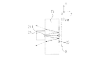
図1a及び1bを基にして、以下に本発明による位置測定装置の第一の変形を説明する。これに関して図1aは走査ユニット20と走査光路を含んだ反射測定尺10の一部の概略的側面図を示す。図1bは図1の走査ユニット20の平面図を示す。
A first variant of the position measuring device according to the invention will be described below on the basis of FIGS. 1a and 1b. In this regard, FIG. 1a shows a schematic side view of a part of a
図示した例において、本発明による位置測定装置は走査ユニット20を備え、この走査ユニットは反射測定尺10と向い合って、測定方向xで可動に設けられている。反射測定尺10と走査ユニット20は、例えば測定方向xで互いに移動可能に設けられた二つの物体、例えば互いに可動な二つの機械部分と接続している。本発明による位置測定装置の位置に依存した出力信号を介して、図示していない後続して設けられた制御ユニットは、機械部分の運動を公知の様式と方法で適切に制御する。
In the illustrated example, the position measuring device according to the present invention comprises a
反射測定尺10は、示した例では直線状のインクリメンタル目盛を備えたトラック、並びにインクリメンタル目盛に対して平行に設けられた、絶対位置検出のための擬似ランダム符号化部を備えたトラックを備えている。トラックは両方とも、適切な目盛担持体、例えば鋼製基体上に配設されている。
The
インクリメンタル目盛を備えたトラックは、測定方向xで周期的に設けられ、様々な光学的反射特性を備えた部分領域から成る。部分領域は目盛平面において、測定方向xに対して垂直に、すなわち与えられたy方向に延在している。この場合、示した実施形態の部分領域は、これにより反射した光束への様々な位相がずれる作用を有する。反射測定尺10はこの例ではいわゆる反射位相格子として形成されている。
A track with an incremental graduation is provided periodically with a measuring direction x and consists of partial areas with various optical reflection characteristics. The partial region extends in the graduation plane perpendicular to the measuring direction x, ie in the given y direction. In this case, the partial area of the illustrated embodiment has the effect of shifting various phases to the reflected light beam. In this example, the
擬似ランダム符号化部を備えたトラックは、測定方向で非周期的に設けられ、様々な光学的反射特性を備えた部分領域から成る。 The track provided with the pseudo-random encoding unit is provided non-periodically in the measurement direction, and is composed of partial regions having various optical reflection characteristics.
走査ユニット20から、図1a及び1bの極めて概略的な描写において、一部だけは識別可能である。すなわち通常、走査ユニット20は適切なケーシングも備えており、このケーシング内には様々な構成部品が同様に設けられている。これらの図では一目瞭然である理由から、本願発明の説明にとって必要な部材だけが示してある。
From the
走査ユニット20の側面では、担持体プリント基板21上に、検出部22.1,22.2を備えた検出ユニット22が設けられている。第一検出部22.1は検出平面内で周期的な縞模様を走査し、かつ多数の位相がずれたインクリメンタル信号を発生させるために使用される。走査された縞模様は反射測定尺10上のインクリメンタル目盛を光学的に走査することから生じる。この場合、第一検出部22.1は、測定方向xで周期的な、個別の検出要素すなわちフォトダイオードの配設による公知の検出部から成る。第二検出部22.2は、公知の様式と方法においては、検出平面内に投影された第二トラックの擬似ランダム符号化部を走査するのに使用される。第二検出部22.2を介して、少なくとも一つの絶対位置信号を発生させることができる。このように生じたインクリメンタル信号と絶対位置信号は、以下に、ことを簡単にするために位置信号と呼ぶ。
On the side surface of the
検出部22.1,22.2は両方とも、本発明による位置測定装置の第一変形においては、ボンディングワイヤ22.3を介して電気的に接続している。すなわち図示していない担持体プリント基板21内のランドパターンと接続している。担持体プリント基板21内のランドパターンを介して、生じた位置信号は図示していない後続して設けられた、引続いての処理のための制御ユニットに供給される。
In the first variant of the position measuring device according to the invention, both detectors 22.1, 22.2 are electrically connected via a bonding wire 22.3. That is, it is connected to a land pattern in the carrier printed board 21 (not shown). Through the land pattern in the carrier printed
両検出部22.1,22.2を備えた検出ユニットの上方には、走査ユニット20の側面で検出部の中央部分領域内に透明な担持基体23が設けられており、例えば板状の硝子担持基体として形成されている。これは本願の例では、例えば図1bから明らかなように、検出部の面全体あるいは検出ユニット22の表面のほんの小さい部分を占めているにすぎない。担持基体23の上側には、担持基体23の第一の側と呼ぶが光源24が配置されている。走査原理が選択される際、例えばいわゆるVCSEL光源のような、いわゆる点光源が光源として機能を果すのが好ましい。光源24は別のボンディングワイヤ24.1を介して電気的に接触しており、このボンディングワイヤは担持基体23の上側で対応する接触部と接続している。ボンディングワイヤ24.1を介して、この接触部は検出ユニット22内の図示していないランドパターンと接続している。
Above the detection unit provided with both detection units 22.1 and 22.2, a
光線を放出する光源24の面は、担持基体23の第一の側の方向に向けられている。従って光源24は反射測定尺10から離間して、担持基体23の下側の方向に発光する。この下側は以下に第二の側と同一に呼ぶ。
The surface of the
担持基体23の下側もしくは第二の側には、光学的反射部材25が設けられており、この反射部材は本願の例においては担持基体23内に一体化された格子構造として、すなわち回折性の光学部材として形成されている。この光学部材の標準的な光学機能性を以下にさらに詳しく説明する。
The lower or second side of the
光源24から到来する光束は、図1aに示したように、反射部材25により反射測定尺10の方向に方向転換され、すなわち反射して戻され、次いで担持基体23を引き返す方向に再度貫通する。続いて部分光束は反射測定尺10に達し、そこで走査ユニット20の方向に再度反射して戻される。最後に走査ユニット20の側で、反射測定尺10から到来する光束が検出平面内に配置された検出部22.1,22.2に達し、そこで走査ユニット20と反射測定尺10が相対運動する場合に、移動量に依存した位置信号が生じる。
インクリメンタル信号の場合、説明した走査光路と、この際結果として生じる部分光束の相互作用を介して、反射測定尺10により、周期的な縞模様が検出平面内に生じる。これは走査ユニット20と反射測定尺10が相対運動する場合に移動量に依存して変調され、かつ検出部22.1,22.2を介して、公知の様式と方法で、かなり位相がずれた別処理するためのインクリメンタル信号に変換される。
すでに冒頭で明らかなように、インクリメンタル信号を生じさせるための本願の原理にとって、使用する光源24を検出平面内にできるだけ配置することが重要である。この場合にだけは、その都度の走査間隔による検出平面内で生じる周期的縞模様の非感度(Unempfindlichkeit)が保証される。この関係に対しては、図2のためのさらに以下の説明がされる。従来技術によれば、このような検出平面内での縞模様周期の変動は受入れられるか、あるいは検出部が取囲まれるキャビティー内において光源が中央に配設されるかのどちらかである。本発明の第一の変形の範囲において、走査光路の巧みな設計によってのみ、特に先に述べた反射部材を備えることにより、代替え的に有利なこれらの問題点の解決可能性は提示される。従って走査航路内での反射部材25の一体化により、光源が走査ユニットの別の場所で事実もしくは実際に、すなわち例えば図1a及び1bで担持基体23の第一の側すなわち上側で明らかなように設けられているが、光源24は検出平面内で仮想で配置されてもよい。
As shown in FIG. 1 a, the light beam coming from the
In the case of an incremental signal, a periodic striped pattern is generated in the detection plane by the
As is already apparent at the outset, it is important for the principle of the present application to generate an incremental signal that the
本発明によるやり方を、図2の作図に基づいてさらに詳しく説明する。これは概略的な様式で、本発明による位置測定装置の第一の変形における一致した重要な幾何学的大きさを含めた展開された走査光路を示している。 The method according to the present invention will be described in more detail with reference to the drawing of FIG. This shows, in a schematic manner, the developed scanning light path including the corresponding important geometric dimensions in the first variant of the position measuring device according to the invention.
図2ではこの場合、反射測定尺を備えた平面はMと表示し、検出平面はDと表示し、LQVIRTは仮想の光源平面を示し、反射部材はREと表示し、LQは実際の光源を示す。大きさT1は走査された測定尺の目盛周期を示しており、T2は検出平面内で結果として生じる周期的縞模様のピッチ周期を示している。座標x_LQVIRTを経由して、走査光路内の仮想光源の位置は測定方向xに沿って示され、座標x_LQREALでもって図1a及び1bで説明したように実際の光源の位置が示される。大きさuは具体的に示したように仮想の光源平面LQVIRTと測定尺平面Mの間の間隔を示しており、大きさvは測定尺平面Mと検出平面Dの間の間隔を示している。 In FIG. 2, in this case, the plane having the reflection measuring scale is indicated as M, the detection plane is indicated as D, LQ VIRT indicates a virtual light source plane, the reflecting member is indicated as RE, and LQ is an actual light source. Indicates. The magnitude T1 indicates the scale period of the scanned measuring scale, and T2 indicates the pitch period of the resulting periodic stripe pattern in the detection plane. Via the coordinate x_LQ VIRT , the position of the virtual light source in the scanning light path is indicated along the measurement direction x, and the actual light source position is indicated by the coordinate x_LQ REAL as described in FIGS. 1a and 1b. The size u indicates the distance between the virtual light source plane LQ VIRT and the measurement scale plane M as specifically shown, and the size v indicates the distance between the measurement scale plane M and the detection plane D. Yes.
本願の場合のような入射光−走査構成の場合、検出平面内で生じる縞模様の周期性は、以下の方程式(1)による周知の幾何学的な考え方に基いて生じる。
T2=T1*(u+v)/v (Gl.1)
仮想的に実際結果として生じるu及びvの変動の場合、すなわち入射光系の走査間隔Δuvの変動の場合、結果として生じる変動ΔT2は、以下の方程式(2)により生じる縞模様の周期において生じる。
ΔT2=T1*Δuv(1−u/v)/v (Gl.2)
この際、Δuvは走査間隔の変数である。
条件u=vを守ると、Gl.(2)の項(1−u/v)は消える。すなわち検出平面D内における縞模様の周期Tは、走査間隔Δuvが場合によっては変動した場合でも、結果としてΔT2=0なので変わらないままである。条件u=vを守ることは、入射光系の場合、光源が検出平面D内に配置されているのと同等である。
In the case of the incident light-scanning configuration as in the present application, the periodicity of the fringe pattern that occurs in the detection plane occurs based on the well-known geometrical concept according to equation (1) below.
T2 = T1 * (u + v) / v (Gl.1)
In the case of fluctuations of u and v virtually resulting as a result, that is, in the case of fluctuations in the scanning interval Δuv of the incident light system, the resulting fluctuation ΔT2 occurs in the period of the fringe pattern produced by the following equation (2).
ΔT2 = T1 * Δuv (1-u / v) / v (Gl.2)
At this time, Δuv is a variable of the scanning interval.
If the condition u = v is observed, Gl. The term (1-u / v) in (2) disappears. That is, the period T of the striped pattern in the detection plane D remains unchanged because ΔT2 = 0 as a result even when the scanning interval Δuv varies depending on the case. Observing the condition u = v is equivalent to the case where the light source is arranged in the detection plane D in the case of the incident light system.
しかしながら図2の図形から明らかであるように、本発明による位置測定装置の第一変形によれば、条件u=vを守ることは、光源LQが光源平面LQVIRT内に設けられるが、実際には位置x_LQREAL内に配置された状態にあることによっても実現できる。このことが図2のようにここに示した位置で反射部材を使用することにより可能になると、これにより一定の様式で、大きさuは先に触れた条件で効果的に調節することができる。実際の光源を検出平面D内に設けることはもはや必要ではないので、光源LQを走査ユニット内に設けることに関する多自由度が結果として生じる。 However, as can be seen from the diagram of FIG. 2, according to the first variant of the position measuring device according to the invention, keeping the condition u = v means that although the light source LQ is provided in the light source plane LQ VIRT , Can also be realized by being located in the position x_LQ REAL . When this is possible by using the reflective member at the position shown here as in FIG. 2, this allows the size u to be adjusted effectively in the above-mentioned conditions in a certain manner. . Since it is no longer necessary to provide an actual light source in the detection plane D, a multi-degree of freedom as a result of providing the light source LQ in the scanning unit results.
各光源と接続する反射部材を構成するための幾つかの可能性を、以下に図3a〜3dに基づき説明する。これらの図は各々概略的な形式で、走査ユニット内で反射部材と光源を配設および/または構成するための様々な変形を示す。 Several possibilities for constructing a reflective member connected to each light source are described below with reference to FIGS. Each of these figures shows, in schematic form, various variations for arranging and / or configuring a reflective member and a light source within a scanning unit.
図3aは、担持基体23の第二の側の光源24’に相対して、反射部材25がこの面で一体化された状態で形成されている一変形を示す。この際反射部材25はこの例では回折性の格子構造体により形成されている。このような格子構造体とは、例えばブレーズ構造を備えた多段式の位相格子か、あるいは理想的ブレーズ格子構造であってもよい。さらに図3aにおいて破線で描かれている場合、仮想光源の位置は、検出平面Dと希望通りに一致する平面LQVIRT内にある。
FIG. 3 a shows a variant in which the reflecting
図3bには、適した反射部材の代替え的な第二実施形態が示してある。わずかに従来例との違いだけを説明する際、機能が同じ部材に関しては従来通り同一の符号を使用する。 FIG. 3b shows an alternative second embodiment of a suitable reflective member. When only the difference from the conventional example is described, the same reference numerals are used for members having the same function as in the past.
図3bでは、担持基体23の第二面側の反射部材25’が光源24’に相対するようにして、所望の光学作用を備えた屈折性の光学部材として形成されている。例えばこれに関しては、担持基体23のこの個所に適したコーティングにより反射鏡が形成され、この反射鏡は、そこから入射する光束への対応する光学反射作用を有する。通常、対応する反射輪郭はこの個所で非球面で形成される。
In FIG. 3b, the reflecting
図3a及び3bの両方の例においては−先行例とは異なり−光源24’は各々、担持基体23と間隔をおいて設けられている。
In both examples of FIGS. 3a and 3b—unlike the previous example—the light sources 24 'are each spaced from the
別の変形が図3cと3dに示してある。この例は先行した二つの例に対して、光源24と光源の電気的接触部を空間的に配設する点が異なっている。従って光源24は各々担持基体23上に直接設けられており、かつ概略的に示した接触部材24.1を介して電気的に導通するように接触する。図3cにおいて、反射部材25は担持基体23上に、再度回折性の格子構造体として形成されており、図3dにおいて、反射部材25’は、所望の光学作用を備えた屈折性の光学部材として形成されている。
Another variation is shown in FIGS. 3c and 3d. This example differs from the preceding two examples in that the
したがって図3cと3dの両方の例において、担持基体23はその光学的機能の他に、各々光源24の位置決めと接触の役割を担っている。その時に光源24のフリップチップ接触が可能である場合、組立時の煩雑な調節も、光源と担持基体を分離させる必要性も無くなる。
Accordingly, in both the examples of FIGS. 3c and 3d, the
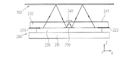
本発明による位置測定装置の第一の変形の別の代替え的実施形態を以下に図4aと4bを基にして説明する。これらの図は、図1a及び1bに類似して、走査光路ための極めて概略的断面図、ならびに走査ユニット200の平面図を再度示している。以下に例えば図1aおよび1bとの重要な相違点だけを説明する。
Another alternative embodiment of the first variant of the position measuring device according to the invention will now be described on the basis of FIGS. 4a and 4b. These figures again show a very schematic cross-sectional view for the scanning light path, as well as a plan view of the
前述の例に類似して、走査ユニット200の面には担持体プリント基板210が設けられており、この担持体プリント基板上には両検出部221,222を備えた検出ユニット220が配置されている。しかしながら、前述とは異なり、その上方に設けられた透明な担持基体230は、明らかに大きな面で形成されており、かつ検出部221,222あるいは検出ユニット220を広範囲に覆っている。これにより、機械的な損傷に対する検出ユニットの保護が確実に改善される。
Similar to the above-described example, a carrier printed
それに加えて前述の例とは異なり、本願の実施形態において、特に検出部221,222の電気的接触が行われる。この場合、担持基体230は電気的接触にも同様に役立つ。光源240の接触のために、第一の例に似て、対応する接触ランドパターン241は担持基体230の上面で延びており、かつ縁部領域では同様に接触パッドで終わっている。これに反して検出部221,222あるいは検出ユニットの電気的接触は、第一の例とは異なり、担持基体230と検出ユニット220の間の担持基体230の下面の別の接触ランドパターン223を介して行われる。したがって、検出部221,222の接触のために、前述の例とは異なり、ボンディングワイヤは全く使用されず、平らに設けられた、担持基体230の下面の接触ランドパターン241,223が使用される。これによりこの構造ユニットを組立てる際、公知のフリップチップ接触方法をしようとすることができる。
In addition, unlike the above-described example, in the embodiment of the present application, the electrical contact of the
さらに根本的な光学的構造は前述の例と同一である。特に担持基体230の第二の側もしくは下面の反射部材250の光学的機能性は、図1a及び1bの光学的機能性に相当する。
Furthermore, the fundamental optical structure is the same as in the previous example. In particular, the optical functionality of the
図5a,5bならびに6を基にして、以下に本発明による位置測定装置の第二変形を説明する。この際図5a及び5bは走査光路を説明するための断面図ならびに使用される走査ユニットの平面図を再度同様に示している。図6a及び6bを基にして、この第二変形の公知の幾何学的な状態を説明する。 A second variant of the position measuring device according to the invention will be described below on the basis of FIGS. 5a and 5b again show a cross-sectional view for explaining the scanning optical path and a plan view of the scanning unit used. Based on FIGS. 6a and 6b, the known geometric state of this second variant is described.
第一変形に基づき説明した、走査光路内に反射部材を設けることにより、光源の位置を検出平面内に仮想的に移すことができる。したがって、特にインクリメンタル走査が走査間隔と所望に独立していることが保証されている。しかしながら公知の所定の幾何学的境界条件を伴う位置関係は存在しており、この位置関係において、反射部材を使用するにもかかわらず、光源の仮想照明点は、検出平面内には存在することにはならず、検出平面の前に存在する。以下に説明する本発明による位置測定装置の第二変形により、適切かつ光学的な、走査光路内での処置により、光源の仮想照明点あるいは検出平面内の仮想光源が存在することになることを保障するために、検出面側での解決手段が提供される。 By providing the reflecting member in the scanning optical path described based on the first modification, the position of the light source can be virtually moved in the detection plane. Thus, it is particularly ensured that the incremental scan is as desired and independent of the scan interval. However, there is a positional relationship with a known predetermined geometric boundary condition. In this positional relationship, the virtual illumination point of the light source exists in the detection plane even though the reflecting member is used. It exists before the detection plane. By means of a second variant of the position measuring device according to the invention described below, an appropriate and optical treatment in the scanning light path will result in the presence of a virtual illumination point of the light source or a virtual light source in the detection plane. In order to ensure, a solution on the detection surface side is provided.
この問題点を解決するのに適切な位置測定装置は、図5及び6において、これまた同様に極めて概略的に示してある。本発明による位置測定装置の第二変形は、図1a及び1bに示した変形に基づいている。以下に第一変形に加えて設けられた処置を説明する。 A suitable position measuring device for solving this problem is shown very schematically in FIGS. 5 and 6 as well. A second variant of the position measuring device according to the invention is based on the variant shown in FIGS. 1a and 1b. The treatment provided in addition to the first modification will be described below.
したがって検出平面において仮想の光源照明点の位置を保証するために、検出部321,322の上方には光学的透過部材360が設けられていてもよい。透過部材360は、公知の光学特性(肉厚d,屈折率n)を備えた、同じ平面上にあるガラス板として形成されており、かつ本例においては、各検出部321,322完全に覆っている。
Therefore, in order to guarantee the position of the virtual light source illumination point on the detection plane, the
走査ユニット300の別の構造、ならびに反射測定尺100は、図1aと1bのそれに対応している。
したがって本発明による位置測定装置の第二変形において、検出平面内での仮想光源の所望の位置を保証するために、担持基体330の下面に反射部材350を設けることに加えて、少なくともインクリメンタル信号を発生させるための検出部321上に光学的透過部材360が設けられる。この位置においては、この付加的な処置は、根本的に反射部材と関連した最初に挙げた処置が無くても使用することができる。すなわち公知の幾何学的境界条件の場合に、単にこれらの処置を講じることで十分であり、かつ第一変形による反射部材を配設するのを止めることで十分である。この場合、例えば検出部の上方で同じ平面上にあるガラス板の形式で、選択された光学的透過部材を走査光路内に設けることは適切である。
Another structure of the
Therefore, in the second modification of the position measuring device according to the present invention, in order to guarantee the desired position of the virtual light source in the detection plane, in addition to providing the reflecting
第二変形と、透過部材により付加的に結果として生じた走査光路への作用を詳しく説明するために、図6a及び6bを参照する。図6aはこれまた同様概略的な形式で様々でかつ関連した幾何学的大きさを含め広げられた走査光路を示している。図6bは図6aの一部分を示している。 In order to explain in detail the second variant and the effect on the scanning light path additionally produced by the transmission member, reference is made to FIGS. 6a and 6b. FIG. 6a also shows the scanning light path widened, including various and related geometrical dimensions, also in schematic form. FIG. 6b shows a portion of FIG. 6a.
根本的に、問題はこのような走査系構成の場合に結果として生じ、くまなく照らされた検出部の面と走査間隔の間に不利な関係があると、第二変形による解決手段を必要とする。したがって、この場合光源の仮想照明点は所望のように検出平面内にはなく、検出平面の前にある。 Fundamentally, the problem arises in the case of such a scanning system configuration, and if there is a disadvantageous relationship between the surface of the detection unit and the scanning interval all over, a solution by the second variant is required. To do. Therefore, in this case, the virtual illumination point of the light source is not in the detection plane as desired, but is in front of the detection plane.
図6a及び6bを基にして、これらの問題、ならびに本発明による位置測定装置の第二変形による、解決手段に関して掌握された処置を詳しく説明する。 Based on FIGS. 6 a and 6 b, these problems, as well as the measures taken for the solution, according to the second variant of the position measuring device according to the invention will be explained in detail.
平面LQREAL内の位置x_LQREALにおける実際の(点)光源から放射される光束は、第一に拡大光学部材(Aufbeitungsoptik)AOを介して適した状態で広げられる。拡大光学部材AOは通常、光学的透過部材として、例えばレンズとして形成されており、かつ肉厚D並びに屈折率n1を有する。放出された光束の示した光線は、入射及び射出の際の拡大光学部材の境界面において、屈折の形態で各々所望の光学作用を受け、かつ角度αにより図6aで示したように、拡大光学部材AO(光線が拡大される)を出る。仮想照明点の位置X_LQVIRTは、伝達される出力光線の破線で描かれた後方への延長部分により見えるように、同じように拡大光学部材AO内で、平面LQVIRTにあるように見えるように生じる。この平面はx1だけ拡大光学部材AOの内側の入射境界面に対してずれている。 The light beam emitted from the actual (point) light source at the position x_LQ REAL in the plane LQ REAL is first spread in a suitable state via an magnifying optical member (Aubeitungoptik) AO. The magnifying optical member AO is usually formed as an optical transmission member, for example, as a lens, and has a thickness D and a refractive index n1. The light rays indicated by the emitted light flux are each subjected to a desired optical action in the form of refraction at the boundary surface of the magnifying optical member upon entry and exit, and magnifying optics as shown in FIG. Exit member AO (light rays are magnified). The position of the virtual illumination point X_LQ VIRT also appears to be in the plane LQ VIRT within the magnifying optical member AO, as seen by the backward extension drawn in broken lines of the transmitted output beam. Arise. This plane is deviated from the incident boundary surface inside the magnifying optical member AO by x1.
間隔uは測定尺平面Mと仮想光源平面LQVIRTの間の間隔を示す。従って測定尺の側から仮想照明点は角度αで現れる。 An interval u indicates an interval between the measurement scale plane M and the virtual light source plane LQ VIRT . Therefore, the virtual illumination point appears at an angle α from the measurement scale side.
すでに先に繰り返し述べたように、大きさuとvは同一、すなわちu=vであることが求められる。言葉で表現すると、このことは、仮想光源平面LQVIRTと測定尺平面Mの間の間隔が、測定尺平面Mと検出平面の間の間隔と同一に選択されることである。 As already described above, it is required that the magnitudes u and v are the same, that is, u = v. In words, this means that the distance between the virtual light source plane LQ VIRT and the measurement scale plane M is selected to be the same as the distance between the measurement scale plane M and the detection plane.
位置測定装置は入射光系として形成されていなければならないので、要求u=vは、検出平面がほとんど拡大光学部材の内側にあることを結果として伴う。しかしながらそこに実際の検出部は配置することはできない。 Since the position measuring device must be formed as an incident light system, the requirement u = v results in that the detection plane is almost inside the magnifying optical member. However, the actual detector cannot be arranged there.
この問題を解決するために、本発明による位置測定装置の第二変形において、検出平面を仮想的に所望の位置に、すなわち仮想の検出平面DVIRT内に持ってくることが考慮される。実際、検出部の配置は、当然適切な実際の検出平面DREAL内で行われる。仮想の検出平面DVIRTは、図6aに示したように、実際の検出平面DREALから間隔x2だけ隔たって設けられている。仮想の検出平面DVIRTを必要な位置に持ってくるために、走査光路には、肉厚dと屈折率n2を備えた光学的透過部材OTが設けられており、従ってそれについては走査光路への一定の光学的作用が結果として生じる。 In order to solve this problem, it is considered in the second variant of the position measuring device according to the invention that the detection plane is virtually brought to the desired position, i.e. in the virtual detection plane D VIRT . In practice, the arrangement of the detectors is naturally performed within the appropriate actual detection plane D REAL . As shown in FIG. 6a, the virtual detection plane D VIRT is provided at a distance x2 from the actual detection plane D REAL . In order to bring the virtual detection plane D VIRT to the required position, an optical transmission member OT having a thickness d and a refractive index n2 is provided in the scanning optical path, so that it is directed to the scanning optical path. Result in certain optical effects.
図6bには、透過部材OTの光学作用が拡大図で示してあり、特にそれにより結果として生じる伝達される光束のための偏向作用が示してある。 In FIG. 6b, the optical action of the transmission member OT is shown in an enlarged view, in particular the deflection action for the resulting transmitted light beam.
以下に、透過部材OTの光学作用、並びに実施形態の考え方を図6aと6bを基にして詳しく説明する。この場合仮想の検出平面DVIRTが同様に仮想の光源平面LVIRT内に導かれることを目指される。仮想の光源平面LVIRTは間隔x1だけ拡大光学部材の表面から遠ざかって存在している。そのことから、検出部の実際の配置が拡大光学部材AOあるいは透過部材OTの外側で行わねばならない場合、x2>x1であることが選択される必要があるという要求が生じる。 Hereinafter, the optical action of the transmission member OT and the concept of the embodiment will be described in detail with reference to FIGS. 6a and 6b. In this case, it is aimed that the virtual detection plane D VIRT is similarly guided into the virtual light source plane L VIRT . The virtual light source plane L VIRT exists away from the surface of the magnifying optical member by an interval x1. For this reason, when the actual arrangement of the detection unit has to be performed outside the magnifying optical member AO or the transmission member OT, a demand arises that x2> x1 needs to be selected.
図6bから明らかなように、透過部材OTの外側の検出部までの光路と位置x_DVIRTにおける検出部までの光路は、実際の光路の場合の、入射境界面において結果として生じる屈折を考慮することで異なる。仮想の光路の場合、このことは図示していないように考慮されない。 As is apparent from FIG. 6b, the optical path to the detection part outside the transmission member OT and the optical path to the detection part at the position x_D VIRT take into account the resulting refraction at the entrance interface in the case of an actual optical path. It is different. In the case of a virtual light path, this is not considered as not shown.
原則的に、入射境界面における実際の光路とみなされている。 In principle, it is regarded as the actual optical path at the entrance interface.
sinα=n2×sinβ (GI.3.1)
さらに、以下の幾何学的関係は図6bにおいて図示した状況とみなされている。
sin α = n2 × sin β (GI 3.1)
Furthermore, the following geometric relationship is considered the situation illustrated in FIG.
tanα=y/x3 (GI.3.2)
tanβ=y/(x3+x2) (GI.3.3)
そのことから、
x3=x2×tanβ/(tanα−tanβ) (GI.3.4)
従って、先に触れた要求x2>x3の下で、大きさd、すなわち透過部材OTの肉厚の選択のための最小限度の条件として生じる。
d=x2+x3
=x1×(1+tanβ/(tanα−tanβ)) (GI.3.5)
走査光路内の透過部材OTの肉厚の相応する選択により、仮想の検出平面の位置は、走査の際の目指される長所を保障するために所望の通りに調節することができる。
tan α = y / x3 (GI.3.2)
tan β = y / (x3 + x2) (GI.3.3)
From that,
x3 = x2 * tan [beta] / (tan [alpha] -tan [beta]) (GI.3.4)
Therefore, under the above-mentioned requirement x2> x3, it occurs as a minimum condition for selection of the size d, that is, the thickness of the transmission member OT.
d = x2 + x3
= X1 × (1 + tan β / (tan α−tan β)) (GI.3.5)
By corresponding selection of the thickness of the transmissive member OT in the scanning optical path, the position of the virtual detection plane can be adjusted as desired to ensure the advantages aimed at during scanning.
図5a及び5bから明らかなように、相応して配置された、適切な肉厚dを有する光学的透過部材は、平行平面のガラス板として形成されており、このガラス板は(実際の)検出部の上方に設けられている。 As can be seen from FIGS. 5a and 5b, the correspondingly arranged optically transmissive members with a suitable thickness d are formed as parallel plane glass plates, which are (actual) detections. It is provided above the part.
さらにまた、光学的透過部材は、本発明による位置測定装置のこの変形において、場合によっては結果として生じる収差を補正するために、例えばレンズ構造あるいは格子構造を備えたような、別の光学的に効果的な構造を備えている。さらに、このような部材を介して、光が検出部にただ垂直に入射し、同時に、傾斜した光の入射による隣接した検出部材間の所望されていない誘導妨害(Uebersprechen)を回避することができる。 Furthermore, the optically transmissive member is a separate optical device, eg with a lens structure or a grating structure, in order to correct the resulting aberrations in this variant of the position measuring device according to the invention. It has an effective structure. Furthermore, through such a member, the light is only incident on the detection unit perpendicularly, and at the same time, undesired inductive interference (Uebersprechen) between adjacent detection members due to the incidence of inclined light can be avoided. .
今まで説明した変形と実施例以外に、本発明の範囲内において、別の代替的でかつ補足するような設計の可能性がある。 In addition to the variations and examples described so far, there are other alternative and complementary design possibilities within the scope of the present invention.
従って、例えば担持基体の上側に各々配置された光源を、適切なシール材料で完全に固め、それにより光源を起こりえる運転の際の損傷から確実に保護することが可能である。 Thus, for example, it is possible to completely secure each light source arranged on the upper side of the carrier substrate with a suitable sealing material, so that it is reliably protected from possible operating damage.
担持基体の上側あるいは下側において、反射部材以外に、必要であれば走査光路に影響を与えるために、別の光学的でかつ効果的な部分領域を形成することができる。この場合、別の回折構造あるいは格子、あるいは別の屈折性の構造または反射器であってもよい。このことは全体として担持基体の一方の側、例えば下側に設けられているか、あるいは形成されているのが好ましい。 In addition to the reflecting member, another optical and effective partial region can be formed on the upper side or the lower side of the supporting substrate in order to influence the scanning optical path if necessary. In this case, it may be a different diffraction structure or grating or another refractive structures or reflector. This is preferably provided or formed on one side, for example the lower side, of the carrier substrate as a whole.
図4a及び4bの実施例により、担持基体が検出ユニットとフリップチップ接触部を介して電気的に接続すると、中間室内には適切な充填材料あるいはいわゆるアンダーフィラーを配置することができ、このアンダーフィラーは、下側に形成された光学的に効果的な担持基体内の構造を保護する。 According to the embodiment of FIGS. 4a and 4b, when the carrier substrate is electrically connected to the detection unit via a flip chip contact, a suitable filling material or so-called underfiller can be placed in the intermediate chamber, this underfiller. Protects the structure within the optically effective carrier substrate formed on the underside.
10 反射測定尺
20 走査ユニット
21 担持プリント基板
22.1 検出部
22.2 検出部
22.3 ボンディングワイヤ
23 担持基体
24 光源
24.1 ボンディングワイヤ
25 反射部材
25’ 反射部材
100 反射測定尺
200 走査ユニット
220 検出ユニット
221 検出部
222 検出部
230 担持基体
240 光源
250 反射部材
300 走査ユニット
320 検出ユニット
321 検出部
322 検出部
340 光源
360 透過部材
d 肉厚
D 検出平面
DVIRT 検出平面
RE 反射部材
u 間隔
v 間隔
x 測定方向
DESCRIPTION OF
Claims (14)
走査ユニット(20;200)内において、さらに少なくとも一つの反射部材(25;25’;250;RE)が走査光路内に設けられており、この反射部材が、一方における仮想の光源と反射測定尺(10;100)の間の間隔(u)と、他方における反射測定尺(10;100)と検出平面(D)の間の間隔(v)が同一であるように走査光路への光学的作用を有しており、これにより光源(24,240)が検出平面(D)内で仮想的に配置されていることを特徴とする位置測定装置。 A position measuring device for capturing at least one of the relative position of the movable reflective measurement grating in measuring direction the scanning unit, and contrast, the position of the scanning unit is provided with a detector in the light source and the detection plane In the measuring device ,
In the scanning unit (20; 200), at least one reflecting member (25; 25 ′; 250; RE) is further provided in the scanning optical path, and this reflecting member is a virtual light source and a reflection measuring scale on one side. The optical effect on the scanning optical path so that the spacing (u) between (10; 100) and the spacing (v) between the reflection measuring scale (10; 100) and the detection plane (D) on the other side are the same. the has, thereby the position measuring apparatus characterized by a light source (24, 240) is virtually arranged in the detection plane (D).
−担持基体の反射測定尺(10;100)に向いた第一の側には、光源(24,240)が設けられており、
−担持基体の反射測定尺(10;100)と反対に向いた第二の側には、反射部材(25;25’;250;RE)が設けられていることを特徴とする請求項1〜4のいずれか記載の位置測定装置。 The scanning unit (20; 200) comprises a transparent carrier substrate (23; 230);
A light source (24, 240) is provided on the first side of the carrier substrate facing the reflection measuring scale (10; 100);
A reflecting member (25; 25 ';250; RE) is provided on the second side of the carrier substrate facing away from the reflection measuring scale (10; 100). 4. The position measuring device according to any one of 4 above.
前記走査ユニット(300)内において、さらに少なくとも一つの光学的透過部材(360)が走査光路内に設けられており、
この透過部材が、一方における光源(340)と反射測定尺(100)の間の間隔(u)と、他方における反射測定尺(100)と仮想の検出平面(DVIRT)内の検出部(321,322)の間の間隔(v)が同一であるように、走査光路への光学的作用を有しており、従って走査ユニット(300)と反射測定尺(100)が相対運動する際に、移動量に依存して変調される縞模様が仮想の検出平面(DVIRT)内で生じており、
走査ユニット(300)が担持プリント基板(310)を備えており、この担持プリント基板上に少なくとも一つの検出部(321,322)を備えた検出ユニット(320)が設けられており、検出部(321,322)の上方には光学的透過部材(360)が設けられており、
光源(340)が検出ユニット(320)の上方に配置されており、従って検出ユニット(320)の平面内への光源(340)の投射部が、検出ユニット(320)の表面の内側にあることを特徴とする位置測定装置。 A position measuring device for capturing the scanning unit, and the relative position of the movable reflective measurement grating in at least one direction of measurement for this, the position where the scanning unit is provided with a detector in the light source and the detection plane In the measuring device ,
In the scanning unit (300), at least one optical transmission member (360) is further provided in the scanning optical path,
This transmission member includes a distance (u) between the light source (340) on one side and the reflection measurement ruler (100), and a detection unit (321) in the reflection measurement ruler (100) on the other side and a virtual detection plane (D VIRT ). , 322) have the same optical effect on the scanning optical path so that the distance (v) between them is the same, so that when the scanning unit (300) and the reflection measuring scale (100) move relative to each other, A fringe pattern that is modulated depending on the amount of movement occurs in the virtual detection plane (D VIRT ) ,
The scanning unit (300) includes a carrier printed circuit board (310), and a detection unit (320) including at least one detection unit (321, 322) is provided on the carrier printed circuit board. 321 and 322) are provided with optically transmissive members (360),
The light source (340) is arranged above the detection unit (320), so that the projection of the light source (340) into the plane of the detection unit (320) is inside the surface of the detection unit (320). A position measuring device characterized by the above.
Applications Claiming Priority (2)
| Application Number | Priority Date | Filing Date | Title |
|---|---|---|---|
| DE102006021017.4 | 2006-05-05 | ||
| DE102006021017A DE102006021017A1 (en) | 2006-05-05 | 2006-05-05 | Position measuring device |
Publications (3)
| Publication Number | Publication Date |
|---|---|
| JP2007298522A JP2007298522A (en) | 2007-11-15 |
| JP2007298522A5 JP2007298522A5 (en) | 2010-05-20 |
| JP4982242B2 true JP4982242B2 (en) | 2012-07-25 |
Family
ID=38288545
Family Applications (1)
| Application Number | Title | Priority Date | Filing Date |
|---|---|---|---|
| JP2007121437A Expired - Fee Related JP4982242B2 (en) | 2006-05-05 | 2007-05-02 | Position measuring device |
Country Status (6)
| Country | Link |
|---|---|
| US (1) | US7473886B2 (en) |
| EP (1) | EP1852684B1 (en) |
| JP (1) | JP4982242B2 (en) |
| CN (1) | CN101067560B (en) |
| DE (1) | DE102006021017A1 (en) |
| ES (1) | ES2389734T3 (en) |
Families Citing this family (15)
| Publication number | Priority date | Publication date | Assignee | Title |
|---|---|---|---|---|
| DE102006021017A1 (en) * | 2006-05-05 | 2007-11-08 | Dr. Johannes Heidenhain Gmbh | Position measuring device |
| DE102007028943A1 (en) | 2007-06-22 | 2008-12-24 | Dr. Johannes Heidenhain Gmbh | Scanning unit for an optical position-measuring device |
| DE102008025870A1 (en) * | 2008-05-31 | 2009-12-03 | Dr. Johannes Heidenhain Gmbh | Optical position measuring device |
| DE102009001262A1 (en) | 2009-03-02 | 2010-09-09 | Dr. Johannes Heidenhain Gmbh | Position measuring device |
| DE102010028725B4 (en) | 2010-05-07 | 2023-05-25 | Dr. Johannes Heidenhain Gmbh | position measuring device |
| US20130148132A1 (en) * | 2010-08-19 | 2013-06-13 | Elesta Relays Gmbh | Sensor head holder |
| JP6032010B2 (en) | 2010-10-12 | 2016-11-24 | 株式会社ニコン | Encoder, drive device and robot device |
| US9383229B2 (en) | 2010-10-31 | 2016-07-05 | Avego Technologies General Ip (Singapore) Pte. Ltd. | Optical reflective encoder with multi-faceted flat-faced lens |
| DE102011007459B4 (en) | 2011-04-15 | 2023-05-11 | Dr. Johannes Heidenhain Gmbh | Optical length measuring device |
| DE102011082570A1 (en) * | 2011-09-13 | 2013-03-14 | Dr. Johannes Heidenhain Gmbh | Rotary position measuring device |
| CN102325233A (en) * | 2011-10-10 | 2012-01-18 | 朱杰 | Contact image sensor with a plurality of scanning arrays |
| EP3009806B1 (en) * | 2014-10-14 | 2016-12-14 | Dr. Johannes Heidenhain GmbH | Position measuring device with means for compensating errors due to thermal dilatation of a scale |
| DE102015219810A1 (en) * | 2015-10-13 | 2017-04-13 | Dr. Johannes Heidenhain Gmbh | X-Y table with a position measuring device |
| TW201741618A (en) * | 2016-05-23 | 2017-12-01 | 國立交通大學 | Optical detecting device |
| GB201916662D0 (en) * | 2019-11-15 | 2020-01-01 | Renishaw Plc | Encoder apparatus |
Family Cites Families (9)
| Publication number | Priority date | Publication date | Assignee | Title |
|---|---|---|---|---|
| US5317149A (en) * | 1992-11-12 | 1994-05-31 | Hewlett-Packard Company | Optical encoder with encapsulated electrooptics |
| US6424407B1 (en) * | 1998-03-09 | 2002-07-23 | Otm Technologies Ltd. | Optical translation measurement |
| MXPA00009038A (en) * | 1998-03-09 | 2002-06-04 | Gou Lite Ltd | Optical translation measurement. |
| JP4812189B2 (en) * | 2001-06-15 | 2011-11-09 | オリンパス株式会社 | Optical detector |
| US6723980B2 (en) * | 2001-07-16 | 2004-04-20 | Wai-Hon Lee | Position sensor with grating to detect moving object with periodic pattern |
| JP4658452B2 (en) * | 2003-02-07 | 2011-03-23 | オリンパス株式会社 | Optical encoder |
| JP4021382B2 (en) * | 2003-07-28 | 2007-12-12 | オリンパス株式会社 | Optical encoder, method of manufacturing the same, and optical lens module |
| US20070120048A1 (en) * | 2005-11-25 | 2007-05-31 | Lum Chee F | Reflective encoder module |
| DE102006021017A1 (en) * | 2006-05-05 | 2007-11-08 | Dr. Johannes Heidenhain Gmbh | Position measuring device |
-
2006
- 2006-05-05 DE DE102006021017A patent/DE102006021017A1/en not_active Withdrawn
-
2007
- 2007-04-17 EP EP07007787A patent/EP1852684B1/en not_active Not-in-force
- 2007-04-17 ES ES07007787T patent/ES2389734T3/en active Active
- 2007-04-30 CN CN2007101023284A patent/CN101067560B/en active Active
- 2007-05-02 JP JP2007121437A patent/JP4982242B2/en not_active Expired - Fee Related
- 2007-05-07 US US11/801,057 patent/US7473886B2/en not_active Expired - Fee Related
Also Published As
| Publication number | Publication date |
|---|---|
| DE102006021017A1 (en) | 2007-11-08 |
| ES2389734T3 (en) | 2012-10-31 |
| CN101067560A (en) | 2007-11-07 |
| EP1852684B1 (en) | 2012-08-15 |
| US7473886B2 (en) | 2009-01-06 |
| CN101067560B (en) | 2011-08-03 |
| US20070262250A1 (en) | 2007-11-15 |
| EP1852684A1 (en) | 2007-11-07 |
| JP2007298522A (en) | 2007-11-15 |
Similar Documents
| Publication | Publication Date | Title |
|---|---|---|
| JP4982242B2 (en) | Position measuring device | |
| JP4021382B2 (en) | Optical encoder, method of manufacturing the same, and optical lens module | |
| US7858922B2 (en) | Position-measuring device | |
| JP5100266B2 (en) | Encoder | |
| JP5005969B2 (en) | Position measuring device | |
| US7417218B2 (en) | Triple grating optical encoder with light transmitting area in optical path | |
| US9383231B2 (en) | Photoelectric encoder having an interference pattern signal processing unit detects the pseudo-random data of the absolute pattern of an absolute scale | |
| US8854630B2 (en) | Position-measuring device | |
| JP4516381B2 (en) | Displacement measuring device | |
| JP4266834B2 (en) | Optical encoder | |
| JP2008129021A (en) | Encoder | |
| JP2005257521A (en) | Optical displacement measuring device | |
| US7876451B2 (en) | Position-measuring device with movable deflection device and grating and with stationary grating, light source, and detector | |
| KR20220097912A (en) | position measuring device | |
| US7705289B2 (en) | Scanning unit for an optical position-measuring device | |
| JP6250525B2 (en) | Encoder | |
| JP2020193929A (en) | Optical encoder | |
| US8937726B2 (en) | Rotary position measuring instrument | |
| JP5069364B2 (en) | Photoelectric incremental encoder | |
| JP5112797B2 (en) | Photoelectric incremental encoder | |
| US20200041252A1 (en) | Optical position measuring device | |
| JP6873760B2 (en) | Position measuring device including an optical distance sensor and an optical distance sensor | |
| JP2010243323A (en) | Optical encoder | |
| JP2017211327A (en) | Light-emitting unit, light-receiving unit and photoelectric encoder | |
| JP5635439B2 (en) | Optical encoder |
Legal Events
| Date | Code | Title | Description |
|---|---|---|---|
| A521 | Request for written amendment filed |
Free format text: JAPANESE INTERMEDIATE CODE: A523 Effective date: 20100402 |
|
| A621 | Written request for application examination |
Free format text: JAPANESE INTERMEDIATE CODE: A621 Effective date: 20100402 |
|
| RD04 | Notification of resignation of power of attorney |
Free format text: JAPANESE INTERMEDIATE CODE: A7424 Effective date: 20100517 |
|
| A131 | Notification of reasons for refusal |
Free format text: JAPANESE INTERMEDIATE CODE: A131 Effective date: 20110830 |
|
| A601 | Written request for extension of time |
Free format text: JAPANESE INTERMEDIATE CODE: A601 Effective date: 20111129 |
|
| A602 | Written permission of extension of time |
Free format text: JAPANESE INTERMEDIATE CODE: A602 Effective date: 20111202 |
|
| A601 | Written request for extension of time |
Free format text: JAPANESE INTERMEDIATE CODE: A601 Effective date: 20111226 |
|
| A602 | Written permission of extension of time |
Free format text: JAPANESE INTERMEDIATE CODE: A602 Effective date: 20120104 |
|
| A521 | Request for written amendment filed |
Free format text: JAPANESE INTERMEDIATE CODE: A523 Effective date: 20120124 |
|
| TRDD | Decision of grant or rejection written | ||
| A01 | Written decision to grant a patent or to grant a registration (utility model) |
Free format text: JAPANESE INTERMEDIATE CODE: A01 Effective date: 20120327 |
|
| A01 | Written decision to grant a patent or to grant a registration (utility model) |
Free format text: JAPANESE INTERMEDIATE CODE: A01 |
|
| A61 | First payment of annual fees (during grant procedure) |
Free format text: JAPANESE INTERMEDIATE CODE: A61 Effective date: 20120423 |
|
| FPAY | Renewal fee payment (event date is renewal date of database) |
Free format text: PAYMENT UNTIL: 20150427 Year of fee payment: 3 |
|
| R150 | Certificate of patent or registration of utility model |
Free format text: JAPANESE INTERMEDIATE CODE: R150 Ref document number: 4982242 Country of ref document: JP Free format text: JAPANESE INTERMEDIATE CODE: R150 |
|
| R250 | Receipt of annual fees |
Free format text: JAPANESE INTERMEDIATE CODE: R250 |
|
| R250 | Receipt of annual fees |
Free format text: JAPANESE INTERMEDIATE CODE: R250 |
|
| R250 | Receipt of annual fees |
Free format text: JAPANESE INTERMEDIATE CODE: R250 |
|
| R250 | Receipt of annual fees |
Free format text: JAPANESE INTERMEDIATE CODE: R250 |
|
| R250 | Receipt of annual fees |
Free format text: JAPANESE INTERMEDIATE CODE: R250 |
|
| R250 | Receipt of annual fees |
Free format text: JAPANESE INTERMEDIATE CODE: R250 |
|
| R250 | Receipt of annual fees |
Free format text: JAPANESE INTERMEDIATE CODE: R250 |
|
| R250 | Receipt of annual fees |
Free format text: JAPANESE INTERMEDIATE CODE: R250 |
|
| LAPS | Cancellation because of no payment of annual fees |