EP1720384A2 - Printed circuit board - Google Patents
Printed circuit board Download PDFInfo
- Publication number
- EP1720384A2 EP1720384A2 EP06252299A EP06252299A EP1720384A2 EP 1720384 A2 EP1720384 A2 EP 1720384A2 EP 06252299 A EP06252299 A EP 06252299A EP 06252299 A EP06252299 A EP 06252299A EP 1720384 A2 EP1720384 A2 EP 1720384A2
- Authority
- EP
- European Patent Office
- Prior art keywords
- printed circuit
- wiring layers
- circuit board
- linear segments
- ground
- Prior art date
- Legal status (The legal status is an assumption and is not a legal conclusion. Google has not performed a legal analysis and makes no representation as to the accuracy of the status listed.)
- Granted
Links
Images

Classifications
-
- H—ELECTRICITY
- H05—ELECTRIC TECHNIQUES NOT OTHERWISE PROVIDED FOR
- H05K—PRINTED CIRCUITS; CASINGS OR CONSTRUCTIONAL DETAILS OF ELECTRIC APPARATUS; MANUFACTURE OF ASSEMBLAGES OF ELECTRICAL COMPONENTS
- H05K1/00—Printed circuits
- H05K1/02—Details
- H05K1/0213—Electrical arrangements not otherwise provided for
- H05K1/0237—High frequency adaptations
- H05K1/025—Impedance arrangements, e.g. impedance matching, reduction of parasitic impedance
- H05K1/0253—Impedance adaptations of transmission lines by special lay-out of power planes, e.g. providing openings
-
- H—ELECTRICITY
- H05—ELECTRIC TECHNIQUES NOT OTHERWISE PROVIDED FOR
- H05K—PRINTED CIRCUITS; CASINGS OR CONSTRUCTIONAL DETAILS OF ELECTRIC APPARATUS; MANUFACTURE OF ASSEMBLAGES OF ELECTRICAL COMPONENTS
- H05K1/00—Printed circuits
- H05K1/02—Details
- H05K1/0213—Electrical arrangements not otherwise provided for
- H05K1/0216—Reduction of cross-talk, noise or electromagnetic interference
- H05K1/0218—Reduction of cross-talk, noise or electromagnetic interference by printed shielding conductors, ground planes or power plane
- H05K1/0224—Patterned shielding planes, ground planes or power planes
-
- H—ELECTRICITY
- H05—ELECTRIC TECHNIQUES NOT OTHERWISE PROVIDED FOR
- H05K—PRINTED CIRCUITS; CASINGS OR CONSTRUCTIONAL DETAILS OF ELECTRIC APPARATUS; MANUFACTURE OF ASSEMBLAGES OF ELECTRICAL COMPONENTS
- H05K1/00—Printed circuits
- H05K1/02—Details
- H05K1/03—Use of materials for the substrate
- H05K1/0393—Flexible materials
-
- H—ELECTRICITY
- H05—ELECTRIC TECHNIQUES NOT OTHERWISE PROVIDED FOR
- H05K—PRINTED CIRCUITS; CASINGS OR CONSTRUCTIONAL DETAILS OF ELECTRIC APPARATUS; MANUFACTURE OF ASSEMBLAGES OF ELECTRICAL COMPONENTS
- H05K2201/00—Indexing scheme relating to printed circuits covered by H05K1/00
- H05K2201/09—Shape and layout
- H05K2201/09209—Shape and layout details of conductors
- H05K2201/09218—Conductive traces
- H05K2201/09236—Parallel layout
-
- H—ELECTRICITY
- H05—ELECTRIC TECHNIQUES NOT OTHERWISE PROVIDED FOR
- H05K—PRINTED CIRCUITS; CASINGS OR CONSTRUCTIONAL DETAILS OF ELECTRIC APPARATUS; MANUFACTURE OF ASSEMBLAGES OF ELECTRICAL COMPONENTS
- H05K2201/00—Indexing scheme relating to printed circuits covered by H05K1/00
- H05K2201/09—Shape and layout
- H05K2201/09209—Shape and layout details of conductors
- H05K2201/09654—Shape and layout details of conductors covering at least two types of conductors provided for in H05K2201/09218 - H05K2201/095
- H05K2201/09681—Mesh conductors, e.g. as a ground plane
-
- Y—GENERAL TAGGING OF NEW TECHNOLOGICAL DEVELOPMENTS; GENERAL TAGGING OF CROSS-SECTIONAL TECHNOLOGIES SPANNING OVER SEVERAL SECTIONS OF THE IPC; TECHNICAL SUBJECTS COVERED BY FORMER USPC CROSS-REFERENCE ART COLLECTIONS [XRACs] AND DIGESTS
- Y10—TECHNICAL SUBJECTS COVERED BY FORMER USPC
- Y10T—TECHNICAL SUBJECTS COVERED BY FORMER US CLASSIFICATION
- Y10T428/00—Stock material or miscellaneous articles
- Y10T428/24—Structurally defined web or sheet [e.g., overall dimension, etc.]
- Y10T428/24802—Discontinuous or differential coating, impregnation or bond [e.g., artwork, printing, retouched photograph, etc.]
- Y10T428/24917—Discontinuous or differential coating, impregnation or bond [e.g., artwork, printing, retouched photograph, etc.] including metal layer
-
- Y—GENERAL TAGGING OF NEW TECHNOLOGICAL DEVELOPMENTS; GENERAL TAGGING OF CROSS-SECTIONAL TECHNOLOGIES SPANNING OVER SEVERAL SECTIONS OF THE IPC; TECHNICAL SUBJECTS COVERED BY FORMER USPC CROSS-REFERENCE ART COLLECTIONS [XRACs] AND DIGESTS
- Y10—TECHNICAL SUBJECTS COVERED BY FORMER USPC
- Y10T—TECHNICAL SUBJECTS COVERED BY FORMER US CLASSIFICATION
- Y10T428/00—Stock material or miscellaneous articles
- Y10T428/24—Structurally defined web or sheet [e.g., overall dimension, etc.]
- Y10T428/24802—Discontinuous or differential coating, impregnation or bond [e.g., artwork, printing, retouched photograph, etc.]
- Y10T428/24926—Discontinuous or differential coating, impregnation or bond [e.g., artwork, printing, retouched photograph, etc.] including ceramic, glass, porcelain or quartz layer
Definitions
- the present invention relates to a printedcircuit board.
- a flexible printed circuit board has for example a wiring layer of conductor formed on one surface of an insulating layer and a ground pattern formed on the other surface.
- Various circuit elements are mounted on the flexible printed circuit board.
- the wiring layer transmits a high frequency signal
- the input/output impedance of the circuit elements and the characteristic impedance of the wiring layer must be matched.
- the capacitance is determined based on the area of the region in which the wiring layers and the ground pattern oppose each other, and therefore the capacitance can be adjusted by adjusting the width of the wiring layer. In this way, the characteristic impedance can be adjusted.
- the width of the wiring layer must be reduced in order to raise the characteristic impedance.
- the limit makes it difficult to raise the characteristic impedance.
- the capacitance may be reduced by increasing the thickness of the insulating layer. When the insulating layer has a large thickness, however, the flexibility of the flexible printed circuit board is deteriorated.
- Fig. 3 is a plan view of an example of a conventional flexible printed circuit board disclosed by JP 5 -343820 A
- Fig. 4 is a sectional view of the flexible printed circuit board in Fig. 3.
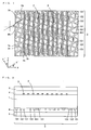
- a plurality of wiring layers 12 are formed on one surface of an insulating layer 11, and a ground pattern 13 is formed on the other surface.
- the ground pattern 13 includes a plurality of ground lines 201 and 202 orthogonal to one another. In this manner, a plurality of square openings 13a are regularly formed.
- the wiring layers 12 are at an angle of 45° with respect to the ground lines 201 and 202.
- cover insulating layers 15 are formed to cover the wiring layers 12 and the ground pattern 13 on the surfaces of the base insulating layer 11 with adhesive layers 14 therebetween.
- the area of the region of the ground pattern 13 opposing the wiring layers 12 can be reduced, and the characteristic impedance of the wiring layers 12 can be increased.
- the invention if there is a positional shift of the wiring layers relative the conductor pattern, variation in the area of the region in which the wiring layers and the conductive pattern oppose each other is reduced. In this way, the positional restriction on the wiring layers in design and the registration accuracy requirement for the wiring layers in the manufacture can be eased.
- Fig. 1 is a plan view of a flexible printedcircuit board according to the embodiment of the invention
- Fig. 2 is a sectional view of the flexible printed circuit board in Fig. 1.
- the flexible printed circuit board will be referred to as "printed circuit board.”
- Fig. 1 the two directions parallel to the surface of a base insulating layer 1 composed for example of polyimide and orthogonal to each other are defined as "X-direction" and "Y-direction.”
- a plurality of wiring layers 2 of conductor such as copper extending in the Y-direction are formed on one surface of the base insulating layer 1.
- a ground pattern 3 of conductor such as copper is formed on the other surface of the base insulating layer 1.
- the ground pattern 3 includes a plurality of integrally formed ground lines 101, 102, and 103.
- the plurality of ground lines 101 are arranged parallel to one another at equal intervals.
- the plurality of ground lines 102 are arranged parallel to one another at equal intervals between adjacent ground lines 101.
- the plurality of ground lines 103 are arranged parallel to one another at equal intervals between the adjacent ground lines 101 and at a predetermined angle with respect to the ground lines 102.
- the ground lines 103 are each formed to connect one end side of one ground line 102 with the other end side of another adjacent ground line 102.
- the ground lines 102 and 103 are arranged at 60° with respect to the ground lines 101.
- the ground lines 101, 102, and 103 form openings 3a and 3b in the shape of a regular triangle.
- the openings 3a and 3b have shapes 180° rotated from each other in the X-Y plane.
- the plurality of openings 3a are arranged both in the X'-direction and the Y'-direction.
- the plurality of openings 3b are arranged both in the X'-direction and the Y'-direction.
- a cover insulating layer 5 of for example polyimide is formed to cover the wiring layers 2 and the ground pattern 3 on both surfaces of the base insulating layer 1 with adhesive layers 4 therebetween.
- the printed circuit board including the base insulating layer 1, the wiring layers 2, the ground pattern 3, the adhesive layers 4, and the cover insulating layers 5 is formed.
- the base insulating layer 1 preferably has a thickness from 5 ⁇ m to 80 ⁇ m, more preferably from 10 ⁇ m to 50 ⁇ m.
- the wiring layer 2 preferably has a width from 10 ⁇ m to 2000 ⁇ m, more preferably from 50 ⁇ m to 1000 ⁇ m.
- the interval between adjacent wiring layers 2 is preferably from 20 ⁇ m to 1000 ⁇ m, more preferably from 50 ⁇ m to 500 ⁇ m.
- the wiring layer 2 preferably has a thickness from 5 ⁇ m to 50 ⁇ m, more preferably from 8 ⁇ m to 40 ⁇ m.
- the ground lines 101, 102, and 103 each preferably have a width from 10 ⁇ m to 2000 ⁇ m, more preferably from 50 ⁇ m to 1000 ⁇ m.
- the ground pattern 3 preferably has a thickness from 5 ⁇ m to 50 ⁇ m, more preferably from 8 ⁇ m to 40 ⁇ m.
- the opening ratio in the ground pattern 3 is preferably from 50% to 70%, more preferably from 55% to 65%.
- the mesh size M1 of the ground pattern 3 is preferably from 0.2 mm to 0.8 mm, more preferably from 0.4 mm to 0.6 mm.
- the mesh size M1 refers to the length of one side of the regular triangle formed by the central lines of the ground lines 101, 102, and 103 (see Fig. 1).
- the angle ? between the X-direction and the X'-direction (ground lines 101) is preferably from 20° to 40 °, more preferably from 25° to 35°, even more preferably from 28° to 32°.
- a method of manufacturing a printed circuit board may be either subtractive process or semi-additive process. Alternatively, subtractive process and semi-additive process may be combined.
- the ground pattern 3 has the openings 3a and 3b, and therefore the area of the region in which the wiring layers 2 and the ground pattern 3 oppose each other is reduced, which reduces the capacitance. In this way, the characteristic impedance of the wiring layers 2 increases. As a result, when the input/output impedance of the circuit elements is high, the input/output impedance of the circuit elements and the characteristic impedance of the wiring layers 2 can be matched. In this way, the characteristic impedance of the wiring layers 2 can arbitrarily be adjusted by adjusting the area of the openings 3a and 3b.
- the openings 3a and 3b in the ground pattern 3 have a triangular shape, and therefore if the position of the wiring layers 2 is shifted in the X-direction (the direction orthogonal to the wiring layers 2), variation in the area of the region in which the wiring layers 2 and the ground pattern 3 oppose each other is reduced.
- the plurality of ground lines 101 are in inclined arrangement at the predetermined angle ? with respect to the X-direction (the direction orthogonal to the wiring layers 2), and therefore if the position of the wiring layers 2 is shifted in the X-direction, variation in the area of the region in which the wiring layers 2 and the ground pattern 3 oppose each other is more reduced. Consequently, the positional restriction on the wiring layers 2 in design and the registration accuracy requirement for the wiring layers 2 in the manufacture can be eased.
- the base insulating layer 1 corresponds to the insulating layer
- the ground pattern 3 corresponds to the conductor pattern
- the ground line 101 corresponds to the first linearsection
- one of the ground lines 102 and 103 corresponds to the second linear section
- the other of the ground lines 103 and 102 corresponds to the third linear section.
- One of the openings 3a and 3b corresponds to the first triangle, and the other of the openings 3b and 3a corresponds to the second triangle.
- the openings 3a and 3b are preferably in the shape of a regular triangle, but the shape may be an isosceles triangle or other triangular shapes.
- the cover insulating layers 5 do not have to be formed on the surfaces of the wiring layer 2 and the ground pattern 3.
- Another insulating layer may be formed on the wiring layers 2 with an adhesive layer therebetween instead of the cover insulating layer 5, and another ground pattern similar to the ground pattern 3 may be formed on the insulating layer thus provided.
- a cover insulating layer may be formed on the other ground pattern with an adhesive layer therebetween.
- the materials for the base insulating layer 1 and the cover insulating layer 5 may include not only polyimide but also other insulating materials such as a polyethylene terephthalate film, a polyethernitrile film, and a polyethersulfone film.
- the materials for the wiring layer 2 and the ground pattern 3 may include not only copper but also other metal materials such as a copper alloy, gold, and aluminum.
- the material for the adhesive layer 4 may include an epoxy-based adhesive, and a polyimide-based adhesive.
- the invention is applied to a flexible printed circuit board, while the invention may be applied to other kinds of printed circuit boards such as a rigid printed circuit board.
- Ten wiring layers 2 extending in the Y-direction were formed on one surface of the base insulating layer 1.
- the wiring layer 2 had a thickness of 12 ⁇ m and a width of 100 ⁇ m.
- the interval between adjacent wiring layers 2 was 100 ⁇ m.
- the ground pattern 3 had a thickness of 12 ⁇ m, and the angle ? formed between the X'-direction and the X-direction and the angle ? formed between the Y'-direction and Y-direction were both 30°.
- the mesh size M1 was 0.5 mm, and the opening ratio in the ground pattern 3 was 60%.
- Ten wiring layers 12 that linearly extend were formed on one surface of a base insulating layer 11.
- the wiring layer 12 had a thickness of 12 ⁇ m and a width of 100 ⁇ m.
- the interval between adjacent wiring layers 12 was 100 ⁇ m.
- the ground pattern 13 has a thickness of 12 ⁇ m.
- the mesh size M2 (the length of one side of the square formed by the central line of each of the ground lines 201 and 202) was 0.5 mm.
- the opening ratio in the ground pattern 13 was 60%.
- the difference between the maximum value and the minimum value of the characteristic impedance of the wiring layer 2 was not more than 10 O.
- the difference between the maximum value and the minimum value of characteristic impedance of the wiring layer 12 was not less than 20 O.
Landscapes
- Engineering & Computer Science (AREA)
- Microelectronics & Electronic Packaging (AREA)
- Structure Of Printed Boards (AREA)
- Chemical And Physical Treatments For Wood And The Like (AREA)
- Polysaccharides And Polysaccharide Derivatives (AREA)
- Manufacturing Of Printed Wiring (AREA)
Abstract
Description
- The present invention relates to a printedcircuit board.
- A flexible printed circuit board has for example a wiring layer of conductor formed on one surface of an insulating layer and a ground pattern formed on the other surface. Various circuit elements are mounted on the flexible printed circuit board. When the wiring layer transmits a high frequency signal, the input/output impedance of the circuit elements and the characteristic impedance of the wiring layer must be matched.
- The characteristic impedance Z of the wiring layer is represented by the following expression:

where C represents the capacitance between the wiring layer and the ground pattern, and L represents the inductance of the wiring layer. - From Expression 1, the capacitance C between the wiring layer and the ground pattern is adjusted, so that the characteristic impedance of the wiring layer can be adjusted.
- The capacitance is determined based on the area of the region in which the wiring layers and the ground pattern oppose each other, and therefore the capacitance can be adjusted by adjusting the width of the wiring layer. In this way, the characteristic impedance can be adjusted.
- When the input/output impedance of the circuit elements is high, the width of the wiring layer must be reduced in order to raise the characteristic impedance. However, there is a limit to how much the width of the wiring layer can be reduced. The limit makes it difficult to raise the characteristic impedance. The capacitance may be reduced by increasing the thickness of the insulating layer. When the insulating layer has a large thickness, however, the flexibility of the flexible printed circuit board is deteriorated.
- A technique of forming regular openings in the ground pattern and reducing the area of the ground pattern has been proposed (see
JP 2000-77802 A JP 5-343820 A - When the area of the ground pattern region opposing the wiring layer is reduced, the capacitance decreases, and the characteristic impedance can be increased.
- Fig. 3 is a plan view of an example of a conventional flexible printed circuit board disclosed by
JP 5 -343820 A - As shown in Figs. 3 and 4, a plurality of
wiring layers 12 are formed on one surface of aninsulating layer 11, and aground pattern 13 is formed on the other surface. - The
ground pattern 13 includes a plurality ofground lines wiring layers 12 are at an angle of 45° with respect to theground lines cover insulating layers 15 are formed to cover thewiring layers 12 and theground pattern 13 on the surfaces of thebase insulating layer 11 withadhesive layers 14 therebetween. - In this way, the area of the region of the
ground pattern 13 opposing thewiring layers 12 can be reduced, and the characteristic impedance of thewiring layers 12 can be increased. - In the conventional flexible printed circuit board described above, when the relative position between the
wiring layers 12 and theground pattern 13 is shifted, the area of the region in which thewiring layers 12 and theground pattern 13 oppose to one another changes. This causes the characteristic impedance of thewiring layers 12 to vary. - Therefore, there is a restriction on the position of the
wiring layers 12 in design. Thewiring layers 12 and theground pattern 13 must be registered with one another with high accuracy in the manufacture. - It is an object of the present invention to provide a printed circuit board that allows the positional restriction on the wiring layers in design and the registration accuracy requirement for the wiring layers in the manufacture to be eased.
- (1) A printed circuit board according to one aspect of the invention includes an insulating layer, a wiring layer formed on one surface of the insulating layer, and a conductor pattern formed on the other surface of the insulating layer, and the conductor pattern has a plurality of regularly formed (e.g. equilateral) triangular openings.
In the printed circuit board, the plurality of openings are formed in the conductor pattern, and therefore the area of the region in which the wiring layers and the conductor pattern oppose each other is reduced. The capacitance between each of the wiring layers and the conductor pattern is reduced, which increases the characteristic impedance of the wiring layers. Consequently, even when the input/output impedance of the circuit elements is high, the input/output impedance of the circuit elements and the characteristic impedance of the wiring layers can be matched. In this way, the characteristic impedance of the wiring layers can arbitrarily be adjusted by adjusting the area of the plurality of openings.
Furthermore, since the openings are in a triangular shape, if there is a positional shift of the wiring layers relative to the conductor pattern, variation in the area of the region in which the wiring layers and the conductor pattern oppose each other is reduced. In this way, the positional restriction on the wiring layers in design and the registration accuracy requirement for the wiring layers in the manufacture can be eased. - (2) The plurality of openings may each have a regular triangle shape. In this way, there are three options for positional relation between each opening and each wiring layer so that equal capacitance is obtained. Thus, the flexibility in positioning the wiring layers in design can be increased.
- (3) The plurality of openings may each have three sides that are not orthogonal to the direction of the wiring layers. In this way, if there is a positional shift of the wiring layers relative to the conductor pattern, variation in the area of the region in which the wiring layers and the conductor pattern oppose each other is more reduced. In this way, the positional restriction on the wiring layers in design and the registration accuracy requirement for the wiring layers in the manufacture can be more eased.
- (4) The plurality of openings may each have one side at an angle of 60° with respect to the direction of the wiring layers. In this way, if there is a positional shift of the wiring layers relative to the conductor pattern, variation in the area of the region in which the wiring layers and the conductor pattern oppose each other is even more reduced. In this way, the positional restriction on the wiring layers in design and the registration accuracy requirement for the wiring layers in the manufacture can be even more eased.
- (5) The conductor pattern may include a plurality of first linear segments parallel to one another, a plurality of second linear segments arranged between adjacent ones of the first linear segments at a first angle with respect to the first linear segments and parallel to one another, and a plurality of third linear segments arranged between adjacent ones of the first linear segments at a second angle with respect to the first linear segments and parallel to one another, the plurality of second and third linear segments may be arranged to form a plurality of first triangles and a plurality of second triangles between adjacent ones of the first linear segments, and the first and second triangles may be 180° rotated from one another in shape on the insulating layer.
In this way, if there is a positional shift of the wiring layers relative to the conductor pattern, variation in the area of the region in which the wiring layers and the conductor pattern oppose each other is sufficiently reduced. Consequently, the positional restriction on the wiring layers in design and the registration accuracy requirement for the wiring layers in the manufacture can sufficiently be eased. - (6) The plurality of first linear segments may be arranged parallel to one another at equal intervals. In this way, if there is a positional shift of the wiring layers relative to the conductor pattern, variation in the area of the region in which the wiring layers and the conductor pattern oppose each other is more reduced. Consequently, the positional restriction on the wiring layers in design and the registration accuracy requirement for the wiring layers in the manufacture can be more eased.
- (7) The plurality of second and third linear segments may have the same length. In this way, each of the openings has an isosceles triangle shape or a regular triangle shape. In this way, there are at least two positional relations that can be selected between each opening and each wiring layer so that equal capacitance is obtained. Consequently, the flexibility in positioning the wiring layers in design can be increased.
- (8) The first and second angles may be 60°. In this way, each of the openings has a regular triangle shape. Consequently, there can be three positional relations that can be selected between each of the openings and each of the wiring layers so that equal capacitance is obtained. Therefore, the flexibility in positioning the wiring layer in design can be increased.
- (9) The first and second triangles may be arranged in directions orthogonal to the plurality of first linear segments. In this way, if there is a positional shift of the wiring layers relative to the conductor pattern, variation in the area of the region in which the wiring layers and the conductor pattern oppose each other is more reduced. Consequently, the positional restriction on the wiring layers in design and the registration accuracy requirement for the wiring layers in the manufacture can be more eased.
- (10) The plurality of first linear segments may be arranged at a third angle other than 90° with respect to the wiring layers. In this way, if there is a positional shift of the wiring layers relative to the conductor pattern, variation in the area of the region in which the wiring layers and the conductor pattern oppose each other is more reduced. Consequently, the positional restriction on the wiring layers in design and the registration accuracy requirement for the wiring layers in the manufacture can be even more eased.
- (11) The third angle may be 60°. In this way, if there is a positional shift of the wiring layers relative to the conductor pattern, variation in the area of the region in which the wiring layers and the conductor pattern oppose each other is sufficiently reduced. Consequently, the positional restriction on the wiring layers in design and the registration accuracy requirement for the wiring layers in the manufacture can sufficiently be eased.
- According to the invention, if there is a positional shift of the wiring layers relative the conductor pattern, variation in the area of the region in which the wiring layers and the conductive pattern oppose each other is reduced. In this way, the positional restriction on the wiring layers in design and the registration accuracy requirement for the wiring layers in the manufacture can be eased.
- Other features, elements, characteristics, and advantages of the present invention will become more apparent from the following description of preferred embodiments of the present invention with reference to the attached drawings.
-
- Fig. 1 is a plan view of a flexible printedcircuit board according to one embodiment of the invention;
- Fig. 2 is a sectional view of the flexible printed circuit board in Fig. 1;
- Fig. 3 is a plan view of a conventional flexible printed circuit board; and
- Fig. 4 is a sectional view of the flexible printed circuit board in Fig. 3.
- Now, a flexible printed circuit board according to one embodiment of the invention will be described with reference to the accompanying drawings.
- Fig. 1 is a plan view of a flexible printedcircuit board according to the embodiment of the invention, and Fig. 2 is a sectional view of the flexible printed circuit board in Fig. 1. Hereinafter, the flexible printed circuit board will be referred to as "printed circuit board."
- In Fig. 1, the two directions parallel to the surface of a base insulating layer 1 composed for example of polyimide and orthogonal to each other are defined as "X-direction" and "Y-direction."
- As shown in Figs. 1 and 2, a plurality of
wiring layers 2 of conductor such as copper extending in the Y-direction are formed on one surface of the base insulating layer 1. Aground pattern 3 of conductor such as copper is formed on the other surface of the base insulating layer 1. - Herein, in Fig. 1, the two directions parallel to the surface of the base insulating layer 1 and at a predetermined angle ? with respect to the X-direction and the Y-direction are defined as "X'-direction" and "Y'-direction."
- As shown in Fig. 1, the
ground pattern 3 includes a plurality of integrally formedground lines ground lines 101 are arranged parallel to one another at equal intervals. - The plurality of
ground lines 102 are arranged parallel to one another at equal intervals between adjacent ground lines 101. The plurality ofground lines 103 are arranged parallel to one another at equal intervals between theadjacent ground lines 101 and at a predetermined angle with respect to the ground lines 102. The ground lines 103 are each formed to connect one end side of oneground line 102 with the other end side of anotheradjacent ground line 102. - According to the embodiment, the
ground lines ground lines form openings 3a and 3b in the shape of a regular triangle. Theopenings 3a and 3b have shapes 180° rotated from each other in the X-Y plane. The plurality of openings 3a are arranged both in the X'-direction and the Y'-direction. The plurality ofopenings 3b are arranged both in the X'-direction and the Y'-direction. - As shown in Fig. 2, a
cover insulating layer 5 of for example polyimide is formed to cover the wiring layers 2 and theground pattern 3 on both surfaces of the base insulating layer 1 withadhesive layers 4 therebetween. - In this way, the printed circuit board including the base insulating layer 1, the wiring layers 2, the
ground pattern 3, theadhesive layers 4, and thecover insulating layers 5 is formed. - The base insulating layer 1 preferably has a thickness from 5 µm to 80 µm, more preferably from 10 µm to 50 µm.
- The
wiring layer 2 preferably has a width from 10 µm to 2000 µm, more preferably from 50 µm to 1000 µm. The interval betweenadjacent wiring layers 2 is preferably from 20 µm to 1000 µm, more preferably from 50 µm to 500 µm. Thewiring layer 2 preferably has a thickness from 5 µm to 50 µm, more preferably from 8 µm to 40 µm. - The ground lines 101, 102, and 103 each preferably have a width from 10 µm to 2000 µm, more preferably from 50 µm to 1000 µm.
- The
ground pattern 3 preferably has a thickness from 5 µm to 50 µm, more preferably from 8 µm to 40 µm. The opening ratio in theground pattern 3 is preferably from 50% to 70%, more preferably from 55% to 65%. The mesh size M1 of theground pattern 3 is preferably from 0.2 mm to 0.8 mm, more preferably from 0.4 mm to 0.6 mm. - The mesh size M1 refers to the length of one side of the regular triangle formed by the central lines of the
ground lines - The angle ? between the X-direction and the X'-direction (ground lines 101) is preferably from 20° to 40 °, more preferably from 25° to 35°, even more preferably from 28° to 32°.
- A method of manufacturing a printed circuit board may be either subtractive process or semi-additive process. Alternatively, subtractive process and semi-additive process may be combined.
- In the printed circuit board according to the embodiment, the
ground pattern 3 has theopenings 3a and 3b, and therefore the area of the region in which the wiring layers 2 and theground pattern 3 oppose each other is reduced, which reduces the capacitance. In this way, the characteristic impedance of the wiring layers 2 increases. As a result, when the input/output impedance of the circuit elements is high, the input/output impedance of the circuit elements and the characteristic impedance of the wiring layers 2 can be matched. In this way, the characteristic impedance of the wiring layers 2 can arbitrarily be adjusted by adjusting the area of theopenings 3a and 3b. - The
openings 3a and 3b in theground pattern 3 have a triangular shape, and therefore if the position of the wiring layers 2 is shifted in the X-direction (the direction orthogonal to the wiring layers 2), variation in the area of the region in which the wiring layers 2 and theground pattern 3 oppose each other is reduced. - The plurality of
ground lines 101 are in inclined arrangement at the predetermined angle ? with respect to the X-direction (the direction orthogonal to the wiring layers 2), and therefore if the position of the wiring layers 2 is shifted in the X-direction, variation in the area of the region in which the wiring layers 2 and theground pattern 3 oppose each other is more reduced. Consequently, the positional restriction on the wiring layers 2 in design and the registration accuracy requirement for the wiring layers 2 in the manufacture can be eased. - In the embodiments described above, the base insulating layer 1 corresponds to the insulating layer, the
ground pattern 3 corresponds to the conductor pattern, theground line 101 corresponds to the first linearsection, one of theground lines ground lines - One of the
openings 3a and 3b corresponds to the first triangle, and the other of theopenings 3b and 3a corresponds to the second triangle. - The
openings 3a and 3b are preferably in the shape of a regular triangle, but the shape may be an isosceles triangle or other triangular shapes. - The
cover insulating layers 5 do not have to be formed on the surfaces of thewiring layer 2 and theground pattern 3. - Another insulating layer may be formed on the wiring layers 2 with an adhesive layer therebetween instead of the
cover insulating layer 5, and another ground pattern similar to theground pattern 3 may be formed on the insulating layer thus provided. In the case, a cover insulating layer may be formed on the other ground pattern with an adhesive layer therebetween. - The materials for the base insulating layer 1 and the
cover insulating layer 5 may include not only polyimide but also other insulating materials such as a polyethylene terephthalate film, a polyethernitrile film, and a polyethersulfone film. - The materials for the
wiring layer 2 and theground pattern 3 may include not only copper but also other metal materials such as a copper alloy, gold, and aluminum. - The material for the
adhesive layer 4 may include an epoxy-based adhesive, and a polyimide-based adhesive. - According to the embodiment described above, the invention is applied to a flexible printed circuit board, while the invention may be applied to other kinds of printed circuit boards such as a rigid printed circuit board.
- In an inventive example, using a flexible printed circuit board according to the embodiment as shown in Figs. 1 and 2, variation in the characteristic impedance of the wiring layer caused by a positional shift of the wiring layer was examined.
- Ten
wiring layers 2 extending in the Y-direction were formed on one surface of the base insulating layer 1. Thewiring layer 2 had a thickness of 12 µm and a width of 100 µm. The interval betweenadjacent wiring layers 2 was 100 µm. - The
ground pattern 3 had a thickness of 12 µm, and the angle ? formed between the X'-direction and the X-direction and the angle ? formed between the Y'-direction and Y-direction were both 30°. The mesh size M1 was 0.5 mm, and the opening ratio in theground pattern 3 was 60%. - In a comparative example, using a conventional flexible printed circuit board as shown in Figs. 3 and 4, variation in the characteristic impedance of the wiring layer caused by a positional shift of the wiring layer was examined.
- Ten wiring layers 12 that linearly extend were formed on one surface of a
base insulating layer 11. Thewiring layer 12 had a thickness of 12 µm and a width of 100 µm. The interval between adjacent wiring layers 12 was 100 µm. - The
ground pattern 13 has a thickness of 12 µm. The mesh size M2 (the length of one side of the square formed by the central line of each of theground lines 201 and 202) was 0.5 mm. The opening ratio in theground pattern 13 was 60%. - All the wiring layers in the printed circuit boards according to the inventive example and the comparative example were measured for their characteristic impedance using a digital oscilloscope according to time domain reflectometry.
- In the inventive example, the difference between the maximum value and the minimum value of the characteristic impedance of the
wiring layer 2 was not more than 10 O. - In the comparative example, the difference between the maximum value and the minimum value of characteristic impedance of the
wiring layer 12 was not less than 20 O. - As can be understood from the foregoing, when the shape of openings in the
ground pattern 3 is a triangle, and the predetermined angle ? is 30° (and the angle formed between thewiring layer 2 and theground line 101 is 60°), variation in the characteristic impedance of thewiring layer 2 caused by the relative positional shift between thewiring layer 2 and theground pattern 3 is reduced. In this way, the positional restriction on the wiring layers 2 in design and the registration accuracy requirement for thewiring layer 2 in the manufacture can be eased. - While preferred embodiments of the present invention have been described above, it is to be understood that variations and modifications will be apparent to those skilled in the art without departing the scope of the present invention.
Claims (11)
- A printed circuit board, comprising:an insulating layer;a wiring layer formed on one surface of said insulating layer; anda conductor pattern formed on the other surface of said insulating layer,said conductor pattern having a plurality of regularly formed triangular openings.
- The printed circuit board according to claim 1, wherein said plurality of openings each have a regular triangle shape.
- The printed circuit board according to claim 1 or 2, wherein said plurality of openings each have three sides that are not orthogonal to the direction of said wiring layer.
- The printed circuit board according to any one of the previous claims, wherein said plurality of openings each have one side at an angle of 60° with respect to the direction of said wiring layer.
- The printed circuit board according to any one of the previous claims, wherein said conductor pattern includes:a plurality of first linear segments parallel to one another;a plurality of second linear segments arranged between adjacent ones of said first linear segments at a first angle with respect to said first linear segments and parallel to one another; anda plurality of third linear segments arranged between adjacent ones of said first linear segments at a second angle with respect to said first linear segments and parallel to one another,said plurality of second and third linear segments are arranged to form a plurality of first triangles and a plurality of second triangles between adjacent said first linear segments, andsaid first and second triangles are 180° rotated from one another in shape on said insulating layer.
- The printed circuitboard according to claim 5, wherein said plurality of first linear segments are arranged parallel to one another at equal intervals.
- The printed circuit board according to claim 5 or 6, wherein said plurality of second and third linear segments have the same length.
- The printed circuit board according to any one of claims 5 to 7, wherein said first and second angles are 60°.
- The printed circuit board according to any one of claims 5 to 8, wherein said first and second triangles are arranged in directions orthogonal to said plurality of first linear segments.
- The printed circuit board according to any one of claims 5 to 9 , wherein said plurality of first linear segments are arranged at a third angle other than 90° with respect to said wiring layer.
- The printed circuit board according to claim 10, wherein said third angle is 60°.
Applications Claiming Priority (1)
| Application Number | Priority Date | Filing Date | Title |
|---|---|---|---|
| JP2005131308A JP3872084B2 (en) | 2005-04-28 | 2005-04-28 | Printed circuit board |
Publications (3)
| Publication Number | Publication Date |
|---|---|
| EP1720384A2 true EP1720384A2 (en) | 2006-11-08 |
| EP1720384A3 EP1720384A3 (en) | 2007-11-21 |
| EP1720384B1 EP1720384B1 (en) | 2010-09-29 |
Family
ID=36999884
Family Applications (1)
| Application Number | Title | Priority Date | Filing Date |
|---|---|---|---|
| EP06252299A Not-in-force EP1720384B1 (en) | 2005-04-28 | 2006-04-28 | Printed circuit board |
Country Status (6)
| Country | Link |
|---|---|
| US (1) | US7473854B2 (en) |
| EP (1) | EP1720384B1 (en) |
| JP (1) | JP3872084B2 (en) |
| CN (1) | CN1856214B (en) |
| AT (1) | ATE483352T1 (en) |
| DE (1) | DE602006017141D1 (en) |
Cited By (3)
| Publication number | Priority date | Publication date | Assignee | Title |
|---|---|---|---|---|
| EP2112871A1 (en) * | 2008-04-22 | 2009-10-28 | Hon Hai Precision Industry Co., Ltd. | Circuit board with improved ground layer |
| US7663063B2 (en) | 2006-12-22 | 2010-02-16 | Hon Hai Precision Industry Co., Ltd. | Circuit board with improved ground plane |
| US20100096170A1 (en) * | 2006-12-22 | 2010-04-22 | Hon Hai Precision Industry Co., Ltd. | Circuit board and layout method thereof |
Families Citing this family (18)
| Publication number | Priority date | Publication date | Assignee | Title |
|---|---|---|---|---|
| JP2008124317A (en) * | 2006-11-14 | 2008-05-29 | Toshiba Matsushita Display Technology Co Ltd | Flexible printed board |
| CN101594732A (en) * | 2008-05-27 | 2009-12-02 | 鸿富锦精密工业(深圳)有限公司 | Circuit board |
| JP4399019B1 (en) * | 2008-07-31 | 2010-01-13 | 株式会社東芝 | Electronic device, flexible printed wiring board, and method for manufacturing flexible printed wiring board |
| KR101256927B1 (en) * | 2009-01-16 | 2013-04-19 | 가부시키가이샤후지쿠라 | Connector and cable assembly |
| CN102473993B (en) * | 2009-07-13 | 2014-01-22 | 株式会社村田制作所 | Signal line and circuit board |
| JP2012094646A (en) * | 2010-10-26 | 2012-05-17 | Daisho Denshi Co Ltd | Printed wiring board corresponding to characteristic impedance control |
| USD720310S1 (en) * | 2011-06-17 | 2014-12-30 | Soraa, Inc. | Triangular semiconductor die |
| KR20130033868A (en) * | 2011-09-27 | 2013-04-04 | 삼성전기주식회사 | Package substrate with mesh pattern and method for manufacturing thereof |
| US8791371B2 (en) | 2011-11-28 | 2014-07-29 | International Business Machines Corporation | Mesh planes with alternating spaces for multi-layered ceramic packages |
| US8952263B2 (en) * | 2012-08-10 | 2015-02-10 | Eastman Kodak Company | Micro-wire electrode pattern |
| US20140216790A1 (en) * | 2013-02-05 | 2014-08-07 | David P. Trauernicht | Conductive micro-wire structure with offset intersections |
| US20140216783A1 (en) * | 2013-02-05 | 2014-08-07 | David P. Trauernicht | Micro-wire pattern with offset intersections |
| TWI457055B (en) * | 2013-02-20 | 2014-10-11 | Novatek Microelectronics Corp | Flexible circuit board and ground line strucure |
| US9536848B2 (en) * | 2014-10-16 | 2017-01-03 | Globalfoundries Inc. | Bond pad structure for low temperature flip chip bonding |
| JP6745712B2 (en) * | 2016-11-30 | 2020-08-26 | 日東電工株式会社 | Wiring circuit board and manufacturing method thereof |
| JP6987700B2 (en) * | 2018-05-29 | 2022-01-05 | 京セラ株式会社 | Printed wiring board |
| EP4329438A4 (en) * | 2021-08-05 | 2025-01-15 | Samsung Electronics Co Ltd | FLEXIBLE CONNECTING ELEMENT AND ELECTRONIC DEVICE THEREFOR |
| CN114786328B (en) * | 2022-05-23 | 2024-04-30 | 西安易朴通讯技术有限公司 | Multilayer printed circuit board |
Citations (3)
| Publication number | Priority date | Publication date | Assignee | Title |
|---|---|---|---|---|
| JPH07302979A (en) | 1994-05-10 | 1995-11-14 | Toshiba Corp | Multilayer interconnection board |
| JPH09275251A (en) | 1996-04-03 | 1997-10-21 | Fujitsu Ltd | Printed wiring board |
| US6184478B1 (en) | 1998-09-30 | 2001-02-06 | Adtec Corporation | Printed wiring device with base layer having a grid pattern |
Family Cites Families (9)
| Publication number | Priority date | Publication date | Assignee | Title |
|---|---|---|---|---|
| US4855537A (en) * | 1987-09-25 | 1989-08-08 | Kabushiki Kaisha Toshiba | Wiring substrate having mesh-shaped earth line |
| JPH05152768A (en) | 1991-11-27 | 1993-06-18 | Nec Corp | Substrate having multilayered-structure |
| JPH05343820A (en) | 1992-06-04 | 1993-12-24 | Toshiba Corp | Circuit board for multichip module |
| JPH06326476A (en) | 1993-05-13 | 1994-11-25 | Sony Corp | Multilayered wiring board |
| JPH07202359A (en) | 1993-12-30 | 1995-08-04 | Sony Corp | Circuit board |
| JPH11298149A (en) | 1998-04-09 | 1999-10-29 | Sumitomo Metal Ind Ltd | Multilayer wiring board |
| TW476229B (en) | 1998-08-24 | 2002-02-11 | Adv Flexible Circuits Co Ltd | Circuit board having shielding plate with empty-hole opening pattern to control impedance and transmission time |
| US6433286B1 (en) * | 2000-09-29 | 2002-08-13 | Intel Corporation | Method of making higher impedance traces on a low impedance circuit board |
| JP2003133659A (en) | 2001-10-19 | 2003-05-09 | Kazunori Aoki | Flexible printed wiring board for high frequency having bending performance |
-
2005
- 2005-04-28 JP JP2005131308A patent/JP3872084B2/en active Active
-
2006
- 2006-04-25 US US11/380,008 patent/US7473854B2/en active Active
- 2006-04-26 CN CN200610076164.8A patent/CN1856214B/en not_active Expired - Fee Related
- 2006-04-28 DE DE602006017141T patent/DE602006017141D1/en active Active
- 2006-04-28 AT AT06252299T patent/ATE483352T1/en not_active IP Right Cessation
- 2006-04-28 EP EP06252299A patent/EP1720384B1/en not_active Not-in-force
Patent Citations (3)
| Publication number | Priority date | Publication date | Assignee | Title |
|---|---|---|---|---|
| JPH07302979A (en) | 1994-05-10 | 1995-11-14 | Toshiba Corp | Multilayer interconnection board |
| JPH09275251A (en) | 1996-04-03 | 1997-10-21 | Fujitsu Ltd | Printed wiring board |
| US6184478B1 (en) | 1998-09-30 | 2001-02-06 | Adtec Corporation | Printed wiring device with base layer having a grid pattern |
Cited By (4)
| Publication number | Priority date | Publication date | Assignee | Title |
|---|---|---|---|---|
| US7663063B2 (en) | 2006-12-22 | 2010-02-16 | Hon Hai Precision Industry Co., Ltd. | Circuit board with improved ground plane |
| US20100096170A1 (en) * | 2006-12-22 | 2010-04-22 | Hon Hai Precision Industry Co., Ltd. | Circuit board and layout method thereof |
| US8256111B2 (en) | 2006-12-22 | 2012-09-04 | Hon Hai Precision Industry Co., Ltd. | Circuit board layout method |
| EP2112871A1 (en) * | 2008-04-22 | 2009-10-28 | Hon Hai Precision Industry Co., Ltd. | Circuit board with improved ground layer |
Also Published As
| Publication number | Publication date |
|---|---|
| JP2006310545A (en) | 2006-11-09 |
| US7473854B2 (en) | 2009-01-06 |
| ATE483352T1 (en) | 2010-10-15 |
| EP1720384A3 (en) | 2007-11-21 |
| JP3872084B2 (en) | 2007-01-24 |
| CN1856214A (en) | 2006-11-01 |
| EP1720384B1 (en) | 2010-09-29 |
| US20060246268A1 (en) | 2006-11-02 |
| DE602006017141D1 (en) | 2010-11-11 |
| CN1856214B (en) | 2010-09-01 |
Similar Documents
| Publication | Publication Date | Title |
|---|---|---|
| EP1720384A2 (en) | Printed circuit board | |
| US6184478B1 (en) | Printed wiring device with base layer having a grid pattern | |
| US8692125B2 (en) | Multilayer substrate | |
| US7096748B2 (en) | Embedded strain gauge in printed circuit boards | |
| KR20070078775A (en) | Manufacturing method of printed wiring board and printed wiring board of multilayer structure | |
| KR20170048575A (en) | Printed wiring board | |
| JP4981618B2 (en) | Printed circuit board | |
| US7375286B2 (en) | Printed circuit board and manufacturing method thereof | |
| KR101333412B1 (en) | Wired circuit board and production method thereof | |
| EP2086297A2 (en) | Printed circuit board and method of manufacturing the same | |
| US11277919B2 (en) | Resin substrate and method for producing resin substrate | |
| US8334462B2 (en) | Wired circuit board assembly sheet including striated portions for enhancing rigidity | |
| US11849544B2 (en) | Milling of flex foil with two conductive layers from both sides | |
| EP2086295B1 (en) | Printed circuit board and method of manufacturing the same | |
| EP2086296A2 (en) | Printed circuit board and method of manufacturing the same | |
| KR100754102B1 (en) | High precision connection member and manufacturing method thereof | |
| JP2006086293A (en) | Printed wiring board and method for designing ground pattern thereof | |
| JP2000151035A (en) | Wiring board and manufacture thereof | |
| US10718791B2 (en) | Probe assembly and probe structure thereof | |
| JP4660738B2 (en) | Printed wiring board and electronic device | |
| JP2009141129A (en) | Flexible printed wiring board and method of manufacturing the same | |
| US6278345B1 (en) | Flexible printed circuit and the method for making the same | |
| US9907158B2 (en) | Wiring structure and printed wiring substrate of wiring structure | |
| US11818837B2 (en) | Circuit board | |
| US20190265274A1 (en) | Probe assembly and probe structure thereof |
Legal Events
| Date | Code | Title | Description |
|---|---|---|---|
| PUAI | Public reference made under article 153(3) epc to a published international application that has entered the european phase |
Free format text: ORIGINAL CODE: 0009012 |
|
| AK | Designated contracting states |
Kind code of ref document: A2 Designated state(s): AT BE BG CH CY CZ DE DK EE ES FI FR GB GR HU IE IS IT LI LT LU LV MC NL PL PT RO SE SI SK TR |
|
| AX | Request for extension of the european patent |
Extension state: AL BA HR MK YU |
|
| PUAL | Search report despatched |
Free format text: ORIGINAL CODE: 0009013 |
|
| AK | Designated contracting states |
Kind code of ref document: A3 Designated state(s): AT BE BG CH CY CZ DE DK EE ES FI FR GB GR HU IE IS IT LI LT LU LV MC NL PL PT RO SE SI SK TR |
|
| AX | Request for extension of the european patent |
Extension state: AL BA HR MK YU |
|
| 17P | Request for examination filed |
Effective date: 20080519 |
|
| AKX | Designation fees paid |
Designated state(s): AT BE BG CH CY CZ DE DK EE ES FI FR GB GR HU IE IS IT LI LT LU LV MC NL PL PT RO SE SI SK TR |
|
| 17Q | First examination report despatched |
Effective date: 20081022 |
|
| GRAP | Despatch of communication of intention to grant a patent |
Free format text: ORIGINAL CODE: EPIDOSNIGR1 |
|
| GRAS | Grant fee paid |
Free format text: ORIGINAL CODE: EPIDOSNIGR3 |
|
| GRAA | (expected) grant |
Free format text: ORIGINAL CODE: 0009210 |
|
| AK | Designated contracting states |
Kind code of ref document: B1 Designated state(s): AT BE BG CH CY CZ DE DK EE ES FI FR GB GR HU IE IS IT LI LT LU LV MC NL PL PT RO SE SI SK TR |
|
| REG | Reference to a national code |
Ref country code: GB Ref legal event code: FG4D |
|
| REG | Reference to a national code |
Ref country code: CH Ref legal event code: EP |
|
| REG | Reference to a national code |
Ref country code: IE Ref legal event code: FG4D |
|
| REF | Corresponds to: |
Ref document number: 602006017141 Country of ref document: DE Date of ref document: 20101111 Kind code of ref document: P |
|
| PG25 | Lapsed in a contracting state [announced via postgrant information from national office to epo] |
Ref country code: AT Free format text: LAPSE BECAUSE OF FAILURE TO SUBMIT A TRANSLATION OF THE DESCRIPTION OR TO PAY THE FEE WITHIN THE PRESCRIBED TIME-LIMIT Effective date: 20100929 Ref country code: FI Free format text: LAPSE BECAUSE OF FAILURE TO SUBMIT A TRANSLATION OF THE DESCRIPTION OR TO PAY THE FEE WITHIN THE PRESCRIBED TIME-LIMIT Effective date: 20100929 Ref country code: LT Free format text: LAPSE BECAUSE OF FAILURE TO SUBMIT A TRANSLATION OF THE DESCRIPTION OR TO PAY THE FEE WITHIN THE PRESCRIBED TIME-LIMIT Effective date: 20100929 |
|
| REG | Reference to a national code |
Ref country code: NL Ref legal event code: VDEP Effective date: 20100929 |
|
| LTIE | Lt: invalidation of european patent or patent extension |
Effective date: 20100929 |
|
| PG25 | Lapsed in a contracting state [announced via postgrant information from national office to epo] |
Ref country code: SI Free format text: LAPSE BECAUSE OF FAILURE TO SUBMIT A TRANSLATION OF THE DESCRIPTION OR TO PAY THE FEE WITHIN THE PRESCRIBED TIME-LIMIT Effective date: 20100929 |
|
| PG25 | Lapsed in a contracting state [announced via postgrant information from national office to epo] |
Ref country code: LV Free format text: LAPSE BECAUSE OF FAILURE TO SUBMIT A TRANSLATION OF THE DESCRIPTION OR TO PAY THE FEE WITHIN THE PRESCRIBED TIME-LIMIT Effective date: 20100929 Ref country code: SE Free format text: LAPSE BECAUSE OF FAILURE TO SUBMIT A TRANSLATION OF THE DESCRIPTION OR TO PAY THE FEE WITHIN THE PRESCRIBED TIME-LIMIT Effective date: 20100929 Ref country code: GR Free format text: LAPSE BECAUSE OF FAILURE TO SUBMIT A TRANSLATION OF THE DESCRIPTION OR TO PAY THE FEE WITHIN THE PRESCRIBED TIME-LIMIT Effective date: 20101230 |
|
| PG25 | Lapsed in a contracting state [announced via postgrant information from national office to epo] |
Ref country code: IS Free format text: LAPSE BECAUSE OF FAILURE TO SUBMIT A TRANSLATION OF THE DESCRIPTION OR TO PAY THE FEE WITHIN THE PRESCRIBED TIME-LIMIT Effective date: 20110129 Ref country code: RO Free format text: LAPSE BECAUSE OF FAILURE TO SUBMIT A TRANSLATION OF THE DESCRIPTION OR TO PAY THE FEE WITHIN THE PRESCRIBED TIME-LIMIT Effective date: 20100929 Ref country code: SK Free format text: LAPSE BECAUSE OF FAILURE TO SUBMIT A TRANSLATION OF THE DESCRIPTION OR TO PAY THE FEE WITHIN THE PRESCRIBED TIME-LIMIT Effective date: 20100929 Ref country code: IT Free format text: LAPSE BECAUSE OF FAILURE TO SUBMIT A TRANSLATION OF THE DESCRIPTION OR TO PAY THE FEE WITHIN THE PRESCRIBED TIME-LIMIT Effective date: 20100929 Ref country code: EE Free format text: LAPSE BECAUSE OF FAILURE TO SUBMIT A TRANSLATION OF THE DESCRIPTION OR TO PAY THE FEE WITHIN THE PRESCRIBED TIME-LIMIT Effective date: 20100929 Ref country code: NL Free format text: LAPSE BECAUSE OF FAILURE TO SUBMIT A TRANSLATION OF THE DESCRIPTION OR TO PAY THE FEE WITHIN THE PRESCRIBED TIME-LIMIT Effective date: 20100929 Ref country code: CZ Free format text: LAPSE BECAUSE OF FAILURE TO SUBMIT A TRANSLATION OF THE DESCRIPTION OR TO PAY THE FEE WITHIN THE PRESCRIBED TIME-LIMIT Effective date: 20100929 Ref country code: PT Free format text: LAPSE BECAUSE OF FAILURE TO SUBMIT A TRANSLATION OF THE DESCRIPTION OR TO PAY THE FEE WITHIN THE PRESCRIBED TIME-LIMIT Effective date: 20110131 |
|
| PG25 | Lapsed in a contracting state [announced via postgrant information from national office to epo] |
Ref country code: BE Free format text: LAPSE BECAUSE OF FAILURE TO SUBMIT A TRANSLATION OF THE DESCRIPTION OR TO PAY THE FEE WITHIN THE PRESCRIBED TIME-LIMIT Effective date: 20100929 |
|
| PG25 | Lapsed in a contracting state [announced via postgrant information from national office to epo] |
Ref country code: ES Free format text: LAPSE BECAUSE OF FAILURE TO SUBMIT A TRANSLATION OF THE DESCRIPTION OR TO PAY THE FEE WITHIN THE PRESCRIBED TIME-LIMIT Effective date: 20110109 |
|
| PLBE | No opposition filed within time limit |
Free format text: ORIGINAL CODE: 0009261 |
|
| STAA | Information on the status of an ep patent application or granted ep patent |
Free format text: STATUS: NO OPPOSITION FILED WITHIN TIME LIMIT |
|
| PG25 | Lapsed in a contracting state [announced via postgrant information from national office to epo] |
Ref country code: PL Free format text: LAPSE BECAUSE OF FAILURE TO SUBMIT A TRANSLATION OF THE DESCRIPTION OR TO PAY THE FEE WITHIN THE PRESCRIBED TIME-LIMIT Effective date: 20100929 Ref country code: DK Free format text: LAPSE BECAUSE OF FAILURE TO SUBMIT A TRANSLATION OF THE DESCRIPTION OR TO PAY THE FEE WITHIN THE PRESCRIBED TIME-LIMIT Effective date: 20100929 |
|
| REG | Reference to a national code |
Ref country code: DE Ref legal event code: R097 Ref document number: 602006017141 Country of ref document: DE Effective date: 20110630 |
|
| PG25 | Lapsed in a contracting state [announced via postgrant information from national office to epo] |
Ref country code: MC Free format text: LAPSE BECAUSE OF NON-PAYMENT OF DUE FEES Effective date: 20110430 |
|
| REG | Reference to a national code |
Ref country code: CH Ref legal event code: PL |
|
| PG25 | Lapsed in a contracting state [announced via postgrant information from national office to epo] |
Ref country code: LI Free format text: LAPSE BECAUSE OF NON-PAYMENT OF DUE FEES Effective date: 20110430 Ref country code: CH Free format text: LAPSE BECAUSE OF NON-PAYMENT OF DUE FEES Effective date: 20110430 |
|
| REG | Reference to a national code |
Ref country code: IE Ref legal event code: MM4A |
|
| PG25 | Lapsed in a contracting state [announced via postgrant information from national office to epo] |
Ref country code: IE Free format text: LAPSE BECAUSE OF NON-PAYMENT OF DUE FEES Effective date: 20110428 |
|
| PG25 | Lapsed in a contracting state [announced via postgrant information from national office to epo] |
Ref country code: CY Free format text: LAPSE BECAUSE OF FAILURE TO SUBMIT A TRANSLATION OF THE DESCRIPTION OR TO PAY THE FEE WITHIN THE PRESCRIBED TIME-LIMIT Effective date: 20100929 Ref country code: LU Free format text: LAPSE BECAUSE OF NON-PAYMENT OF DUE FEES Effective date: 20110428 |
|
| PG25 | Lapsed in a contracting state [announced via postgrant information from national office to epo] |
Ref country code: TR Free format text: LAPSE BECAUSE OF FAILURE TO SUBMIT A TRANSLATION OF THE DESCRIPTION OR TO PAY THE FEE WITHIN THE PRESCRIBED TIME-LIMIT Effective date: 20100929 Ref country code: BG Free format text: LAPSE BECAUSE OF FAILURE TO SUBMIT A TRANSLATION OF THE DESCRIPTION OR TO PAY THE FEE WITHIN THE PRESCRIBED TIME-LIMIT Effective date: 20101229 |
|
| PG25 | Lapsed in a contracting state [announced via postgrant information from national office to epo] |
Ref country code: HU Free format text: LAPSE BECAUSE OF FAILURE TO SUBMIT A TRANSLATION OF THE DESCRIPTION OR TO PAY THE FEE WITHIN THE PRESCRIBED TIME-LIMIT Effective date: 20100929 |
|
| REG | Reference to a national code |
Ref country code: FR Ref legal event code: PLFP Year of fee payment: 11 |
|
| REG | Reference to a national code |
Ref country code: FR Ref legal event code: PLFP Year of fee payment: 12 |
|
| REG | Reference to a national code |
Ref country code: FR Ref legal event code: PLFP Year of fee payment: 13 |
|
| PGFP | Annual fee paid to national office [announced via postgrant information from national office to epo] |
Ref country code: FR Payment date: 20190313 Year of fee payment: 14 |
|
| PGFP | Annual fee paid to national office [announced via postgrant information from national office to epo] |
Ref country code: DE Payment date: 20190416 Year of fee payment: 14 |
|
| PGFP | Annual fee paid to national office [announced via postgrant information from national office to epo] |
Ref country code: GB Payment date: 20190424 Year of fee payment: 14 |
|
| REG | Reference to a national code |
Ref country code: DE Ref legal event code: R119 Ref document number: 602006017141 Country of ref document: DE |
|
| PG25 | Lapsed in a contracting state [announced via postgrant information from national office to epo] |
Ref country code: DE Free format text: LAPSE BECAUSE OF NON-PAYMENT OF DUE FEES Effective date: 20201103 Ref country code: FR Free format text: LAPSE BECAUSE OF NON-PAYMENT OF DUE FEES Effective date: 20200430 |
|
| GBPC | Gb: european patent ceased through non-payment of renewal fee |
Effective date: 20200428 |
|
| PG25 | Lapsed in a contracting state [announced via postgrant information from national office to epo] |
Ref country code: GB Free format text: LAPSE BECAUSE OF NON-PAYMENT OF DUE FEES Effective date: 20200428 |