EP1719971A1 - Optical stacked structure inspecting method and optical stacked structure inspecting apparatus - Google Patents
Optical stacked structure inspecting method and optical stacked structure inspecting apparatus Download PDFInfo
- Publication number
- EP1719971A1 EP1719971A1 EP06252430A EP06252430A EP1719971A1 EP 1719971 A1 EP1719971 A1 EP 1719971A1 EP 06252430 A EP06252430 A EP 06252430A EP 06252430 A EP06252430 A EP 06252430A EP 1719971 A1 EP1719971 A1 EP 1719971A1
- Authority
- EP
- European Patent Office
- Prior art keywords
- stacked structure
- light
- optical
- layer
- substrate
- Prior art date
- Legal status (The legal status is an assumption and is not a legal conclusion. Google has not performed a legal analysis and makes no representation as to the accuracy of the status listed.)
- Granted
Links
- 230000003287 optical effect Effects 0.000 title claims abstract description 125
- 238000000034 method Methods 0.000 title claims abstract description 35
- 239000000758 substrate Substances 0.000 claims abstract description 80
- 239000010409 thin film Substances 0.000 claims abstract description 38
- 238000007689 inspection Methods 0.000 claims abstract description 14
- 230000001678 irradiating effect Effects 0.000 claims description 2
- 239000011368 organic material Substances 0.000 claims 16
- 239000010410 layer Substances 0.000 description 133
- 239000000975 dye Substances 0.000 description 52
- 238000002310 reflectometry Methods 0.000 description 38
- 238000010586 diagram Methods 0.000 description 24
- 238000004544 sputter deposition Methods 0.000 description 16
- 238000001228 spectrum Methods 0.000 description 10
- VYPSYNLAJGMNEJ-UHFFFAOYSA-N Silicium dioxide Chemical compound O=[Si]=O VYPSYNLAJGMNEJ-UHFFFAOYSA-N 0.000 description 9
- 238000002835 absorbance Methods 0.000 description 8
- 238000005259 measurement Methods 0.000 description 7
- 239000000203 mixture Substances 0.000 description 7
- 239000011295 pitch Substances 0.000 description 7
- 238000010521 absorption reaction Methods 0.000 description 6
- 239000000463 material Substances 0.000 description 6
- 239000004417 polycarbonate Substances 0.000 description 5
- 229920000515 polycarbonate Polymers 0.000 description 5
- 229910052984 zinc sulfide Inorganic materials 0.000 description 5
- 239000000853 adhesive Substances 0.000 description 4
- 229910052681 coesite Inorganic materials 0.000 description 4
- 229910052906 cristobalite Inorganic materials 0.000 description 4
- 239000000377 silicon dioxide Substances 0.000 description 4
- 229910052682 stishovite Inorganic materials 0.000 description 4
- 229910052905 tridymite Inorganic materials 0.000 description 4
- 238000000862 absorption spectrum Methods 0.000 description 3
- 230000006866 deterioration Effects 0.000 description 3
- 229910052751 metal Inorganic materials 0.000 description 3
- 239000002184 metal Substances 0.000 description 3
- 239000011347 resin Substances 0.000 description 3
- 229920005989 resin Polymers 0.000 description 3
- 230000003595 spectral effect Effects 0.000 description 3
- XLOMVQKBTHCTTD-UHFFFAOYSA-N Zinc monoxide Chemical compound [Zn]=O XLOMVQKBTHCTTD-UHFFFAOYSA-N 0.000 description 2
- XJHCXCQVJFPJIK-UHFFFAOYSA-M caesium fluoride Chemical compound [F-].[Cs+] XJHCXCQVJFPJIK-UHFFFAOYSA-M 0.000 description 2
- 150000001875 compounds Chemical class 0.000 description 2
- 229910052737 gold Inorganic materials 0.000 description 2
- 238000004519 manufacturing process Methods 0.000 description 2
- 238000001552 radio frequency sputter deposition Methods 0.000 description 2
- 229910052709 silver Inorganic materials 0.000 description 2
- 229910052581 Si3N4 Inorganic materials 0.000 description 1
- GWEVSGVZZGPLCZ-UHFFFAOYSA-N Titan oxide Chemical compound O=[Ti]=O GWEVSGVZZGPLCZ-UHFFFAOYSA-N 0.000 description 1
- 239000005083 Zinc sulfide Substances 0.000 description 1
- 239000000956 alloy Substances 0.000 description 1
- 229910045601 alloy Inorganic materials 0.000 description 1
- 229910052782 aluminium Inorganic materials 0.000 description 1
- 238000000137 annealing Methods 0.000 description 1
- 239000000987 azo dye Substances 0.000 description 1
- OYLGJCQECKOTOL-UHFFFAOYSA-L barium fluoride Chemical compound [F-].[F-].[Ba+2] OYLGJCQECKOTOL-UHFFFAOYSA-L 0.000 description 1
- 229910001632 barium fluoride Inorganic materials 0.000 description 1
- 239000011248 coating agent Substances 0.000 description 1
- 238000000576 coating method Methods 0.000 description 1
- 229910052802 copper Inorganic materials 0.000 description 1
- PMHQVHHXPFUNSP-UHFFFAOYSA-M copper(1+);methylsulfanylmethane;bromide Chemical compound Br[Cu].CSC PMHQVHHXPFUNSP-UHFFFAOYSA-M 0.000 description 1
- 230000007423 decrease Effects 0.000 description 1
- 230000007547 defect Effects 0.000 description 1
- 230000002542 deteriorative effect Effects 0.000 description 1
- 239000003989 dielectric material Substances 0.000 description 1
- 238000010828 elution Methods 0.000 description 1
- 150000004673 fluoride salts Chemical class 0.000 description 1
- 229910052738 indium Inorganic materials 0.000 description 1
- -1 ion compounds Chemical class 0.000 description 1
- 229910052749 magnesium Inorganic materials 0.000 description 1
- 239000011777 magnesium Substances 0.000 description 1
- ORUIBWPALBXDOA-UHFFFAOYSA-L magnesium fluoride Chemical compound [F-].[F-].[Mg+2] ORUIBWPALBXDOA-UHFFFAOYSA-L 0.000 description 1
- 229910001635 magnesium fluoride Inorganic materials 0.000 description 1
- 238000012986 modification Methods 0.000 description 1
- 230000004048 modification Effects 0.000 description 1
- CWQXQMHSOZUFJS-UHFFFAOYSA-N molybdenum disulfide Chemical compound S=[Mo]=S CWQXQMHSOZUFJS-UHFFFAOYSA-N 0.000 description 1
- 150000004767 nitrides Chemical class 0.000 description 1
- 239000012044 organic layer Substances 0.000 description 1
- TWNQGVIAIRXVLR-UHFFFAOYSA-N oxo(oxoalumanyloxy)alumane Chemical compound O=[Al]O[Al]=O TWNQGVIAIRXVLR-UHFFFAOYSA-N 0.000 description 1
- 229910052763 palladium Inorganic materials 0.000 description 1
- 239000004033 plastic Substances 0.000 description 1
- 229910052697 platinum Inorganic materials 0.000 description 1
- HQVNEWCFYHHQES-UHFFFAOYSA-N silicon nitride Chemical compound N12[Si]34N5[Si]62N3[Si]51N64 HQVNEWCFYHHQES-UHFFFAOYSA-N 0.000 description 1
- 229910052814 silicon oxide Inorganic materials 0.000 description 1
- 238000004528 spin coating Methods 0.000 description 1
- VDNSGQQAZRMTCI-UHFFFAOYSA-N sulfanylidenegermanium Chemical compound [Ge]=S VDNSGQQAZRMTCI-UHFFFAOYSA-N 0.000 description 1
- 150000004763 sulfides Chemical class 0.000 description 1
- 229910052715 tantalum Inorganic materials 0.000 description 1
- 239000013077 target material Substances 0.000 description 1
- ANRHNWWPFJCPAZ-UHFFFAOYSA-M thionine Chemical compound [Cl-].C1=CC(N)=CC2=[S+]C3=CC(N)=CC=C3N=C21 ANRHNWWPFJCPAZ-UHFFFAOYSA-M 0.000 description 1
- 239000010936 titanium Substances 0.000 description 1
- 229910052719 titanium Inorganic materials 0.000 description 1
- OGIDPMRJRNCKJF-UHFFFAOYSA-N titanium oxide Inorganic materials [Ti]=O OGIDPMRJRNCKJF-UHFFFAOYSA-N 0.000 description 1
- 238000002834 transmittance Methods 0.000 description 1
- 229910052720 vanadium Inorganic materials 0.000 description 1
- 229910052725 zinc Inorganic materials 0.000 description 1
- 239000011701 zinc Substances 0.000 description 1
- 239000011787 zinc oxide Substances 0.000 description 1
- DRDVZXDWVBGGMH-UHFFFAOYSA-N zinc;sulfide Chemical compound [S-2].[Zn+2] DRDVZXDWVBGGMH-UHFFFAOYSA-N 0.000 description 1
Images



Classifications
-
- G—PHYSICS
- G01—MEASURING; TESTING
- G01N—INVESTIGATING OR ANALYSING MATERIALS BY DETERMINING THEIR CHEMICAL OR PHYSICAL PROPERTIES
- G01N21/00—Investigating or analysing materials by the use of optical means, i.e. using sub-millimetre waves, infrared, visible or ultraviolet light
- G01N21/84—Systems specially adapted for particular applications
- G01N21/88—Investigating the presence of flaws or contamination
- G01N21/95—Investigating the presence of flaws or contamination characterised by the material or shape of the object to be examined
- G01N21/9506—Optical discs
-
- G—PHYSICS
- G01—MEASURING; TESTING
- G01B—MEASURING LENGTH, THICKNESS OR SIMILAR LINEAR DIMENSIONS; MEASURING ANGLES; MEASURING AREAS; MEASURING IRREGULARITIES OF SURFACES OR CONTOURS
- G01B11/00—Measuring arrangements characterised by the use of optical techniques
- G01B11/02—Measuring arrangements characterised by the use of optical techniques for measuring length, width or thickness
- G01B11/06—Measuring arrangements characterised by the use of optical techniques for measuring length, width or thickness for measuring thickness ; e.g. of sheet material
- G01B11/0616—Measuring arrangements characterised by the use of optical techniques for measuring length, width or thickness for measuring thickness ; e.g. of sheet material of coating
- G01B11/0625—Measuring arrangements characterised by the use of optical techniques for measuring length, width or thickness for measuring thickness ; e.g. of sheet material of coating with measurement of absorption or reflection
Definitions
- the present invention generally relates to optical stacked structure inspecting methods and optical stacked structure inspecting apparatuses, and more particularly to an optical stacked structure inspecting method and an optical stacked structure inspecting apparatus for inspecting a dye layer thickness and/or a dielectric layer thickness of an optical stacked structure in which a reflection layer and an organic dye layer are successively stacked on a substrate or, a reflection layer, an organic dye layer and a dielectric layer are successively stacked on a substrate.
- the present invention also relates to a method and an apparatus for producing such an optical stacked structure.
- Such write-once type optical recording media to which information can be written once by a laser beam, include CD-R, DVD+R and DVD-R.
- Such write-once type optical recording media have a stacked structure made up of a transparent polycarbonate substrate formed with a tracking groove, a recording layer made of an organic dye spin-coated on the substrate, a light reflection layer made of Au or Ag sputtered on the recording layer, and a projection layer made of an ultraviolet curing resin that are stacked in this order.
- the DVD+R and the DVD-R have a structure in which two substrates having a thickness of 0.6 mm are bonded together, and have a large recording capacity.
- a Japanese Laid-Open Patent Application No.2002-510107 proposes a method of measuring the layer thickness based on transmitted or reflected light that is diffracted by the groove.
- a Japanese Laid-Open Patent Application No.2002-367244 proposes a method of measuring the thicknesses of a land part and a groove part based on diffracted light of different orders, and inspecting the dye layer thickness by measuring the transmittance and the diffracted light intensity in a state where the dye layer is formed on the substrate.
- a Japanese Laid-Open Patent Application No.11-66633 proposes an apparatus for inspecting defects from the reflected light using, as the inspection light, light having a characteristic absorption wavelength of the dye as a main component.
- the existing DVD-ROMs for read use include those having two information recording layers for the purpose of increasing the recording capacity.
- a first substrate and a second substrate are bonded via a transparent intermediate layer made of an ultraviolet curing resin.
- a first information recording layer L0 has a semi-transparent first layer formed on an inner surface of the first substrate formed with concavo-convex pits.
- a second information recording layer L1 has the transparent intermediate layer and a metal reflecting second layer formed on the first information recording layer L0.
- the semi-transparent first layer is formed by a dielectric layer or a thin metal layer.
- This type of optical recording medium is made up of a first substrate and a second substrate that are bonded via an adhesive agent.
- the first substrate includes a transparent substrate formed with a groove, a recording layer made of an organic dye formed on the substrate, a semi-transparent reflection layer formed on the recording layer, and an ultraviolet curing resin formed on the recording layer, that are stacked in this order.
- the second substrate includes a substrate formed with a groove, a total reflection layer formed on the substrate, a recording layer made of an organic dye formed on the substrate, and a transparent organic thin film formed on the recording layer, that are stacked in this order. Examples of this type of optical recording media are proposed in Japanese Laid-Open Patent Applications No.10-340483 and No.2000-311384 .
- Another and more specific object of the present invention is to provide an optical stacked structure inspecting methods, an optical stacked structure inspecting apparatus, an optical stacked structure producing method and an optical stacked structure producing apparatus, which enable simple inspection of the thickness of each layer of the optical stacked structure having a reflection layer and at least one light transmitting thin film stacked on a substrate.
- Still another object of the present invention is to provide an optical stacked structure inspecting method for inspecting an optical stacked structure having a reflection layer and at least one light transmitting thin film sequentially stacked on a substrate, characterized in that the optical stacked structure inspecting method comprises the steps of (a) irradiating inspection light on the optical stacked structure from a side provided with the light transmitting thin film; (b) measuring a light intensity of reflected light from each layer, that changes depending on a change in an optical path length to each layer; and (c) inspecting a thickness of the light transmitting thin film based on the light intensity of reflected light for a specific wavelength.
- the optical stacked structure inspecting method of the present invention it is possible to enable simple inspection of the thickness of each layer of the optical stacked structure.
- a further object of the present invention is to provide an optical stacked structure inspecting apparatus for inspecting an optical stacked structure having a reflection layer and at least one light transmitting thin film sequentially stacked on a substrate, characterized in that the optical stacked structure inspecting apparatus comprises a light source configured to irradiate inspection light on the optical stacked structure from a side provided with the light transmitting thin film, and an inspecting part configured to measuring a light intensity of reflected light from each layer, that changes depending on a change in an optical path length to each layer, and to inspect a thickness of the light transmitting thin film based on the light intensity of reflected light for a specific wavelength.
- the optical stacked structure inspecting apparatus of the present invention it is possible to enable simple inspection of the thickness of each layer of the optical stacked structure.
- FIG. 1 is a diagram generally showing a structure of the optical stacked structure inspecting apparatus in a first embodiment of the present invention, for explaining the optical stacked structure inspecting method and the optical stacked structure inspecting apparatus according to the present invention.
- the present invention is applied to the inspection process (or checking process) for a second substrate of the write-once type optical recording medium having the recording layer with the two-layer structure when producing this write-once type optical recording medium.
- a light source 1 is made of a light emitting diode and emits light in a direction indicated by an arrow.
- a condenser lens 2 forms the light from the light source 1 into parallel rays which pass a beam splitter 3, and light having an intensity of approximately 50% of that of the parallel rays reaches a second substrate within an optical stacked structure 4, that is, the write-once type optical recording medium having the recording layer with the two-layer structure.
- Remaining light split by the beam splitter 3 is monitored by an incident light photosensor 5 to measure the incident light intensity.
- the light reflected at the surface of the second substrate of the optical stacked structure 4 passes through the beam splitter 3 again and is received by a reflected light photosensor 6 to measure the reflected light intensity.
- a light separating means 7 may be provided at a stage preceding the incident light photosensor 5 with respect to the incoming light to the incident light photosensor 5 to separate a specific wavelength
- a light separating means 8 may be provided at a stage preceding the reflected light photosensor 6 with respect to the incoming light to the reflected light photosensor 6 to separate a specific wavelength
- the light separating means 7 may be formed by a prism or a diffraction grating.
- An inspecting part 9 compares the incident light intensity measured by the incident light photosensor 5 and the reflected light intensity measured by the reflected light photosensor 6, and obtains the reflectivity of the light emitting wavelength of the light emitting diode forming the light source 1.
- the optical stacked structure 4 that is, the write-once type optical recording medium having the recording layer with the two-layer structure, has a first substrate and the second substrate that are bonded using an adhesive agent.
- the first substrate has a tracking groove having a depth of 20 nm to 200 nm arranged at a pitch of 0.74 ⁇ m on a disk-shaped substrate surface.
- an organic dye layer having an absorption spectrum with a maximum absorption wavelength of 580 nm to 620 nm is coated on the total reflection layer.
- a dye compound that can easily obtain a desired optical characteristic in the laser beam wavelength for DVD of approximately 650 nm such as tetraazaporphyrazine dye, cyanine dye, azo dye and squarylium dye, may be used for the organic dye layer.
- the second substrate has a dye layer, a semi-transparent reflection layer, and a transparent dielectric layer that are stacked on the substrate surface. The transparent dielectric layer is provided to prevent elution of the dye coated on the first substrate when the first and second substrate are bonded using the adhesive agent.
- the transparent dielectric layer is desirably a compact thin layer that bonds satisfactorily with respect to the dye.
- the transparent dielectric layer may be made of oxides such as silicon oxide, aluminum oxide, zinc oxide and titanium oxide, nitrides such as silicon nitride and aluminum nitride, sulfides such as zinc sulfide, germanium sulfide and molybdenum sulfide, fluorides such as magnesium fluoride, cesium fluoride and barium fluoride, and suitable mixtures of such.
- the absorbance and reflectivity of the optical stacked structure 4 were obtained by measuring the spectral reflectivity using ETA-RT manufactured by STEAG ETA-Optik.
- the Ag total reflection layer had a reflectivity spectrum with a high reflectivity in a visible light region, a slightly lower reflectivity in a short wavelength region, and a higher reflectivity in a long wavelength region.
- this Ag reflection layer was formed on the optical stacked structure 4 having grooves formed at equal pitches on a plastic substrate, a deterioration in the reflectivity caused by the diffraction at the grooves was observed. This deterioration in the reflectivity became greater as the depth of the grooves became deeper, and as the pitch of the grooves became smaller, the wavelengths at which the reflectivity deteriorates shifted towards the short wavelengths approximately proportionally to the pitch.
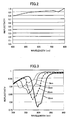
- FIG. 2 is a diagram showing a relationship of the reflectivity and wavelength for a case where Ag was formed to a thickness of 140 nm on a polycarbonate substrate having the grooves having a depth of 33 nm and a width of 0.25 ⁇ m formed at a pitch of 0.74 ⁇ m.
- FIG. 2 shows the spectral reflection spectrum of the light that is perpendicularly incident to and reflects perpendicularly from the Ag total reflection layer. In this case, a phenomenon in which the reflectivity decreases by 5% to 6% due to scattering at the grooves was observed in a vicinity of the wavelength of 750 nm.
- FIG. 3 is a diagram showing a relationship of the reflectivity and wavelength for a case where a dielectric layer, having a composition ZnS (80 mol%) /SiO 2 (20 mol%), was formed to a thickness of 10 nm to 30 nm on the polycarbonate substrate formed with the Ag total reflection layer.
- FIG. 3 shows the spectral reflection spectrum of the light that is perpendicularly incident to and reflects perpendicularly from the surface formed with the dielectric layer.
- the wavelengths at which the minimum reflectivity is obtained shifted towards the long wavelengths in the reflectivity deteriorating portion where the wavelength is 700 nm to 850 nm, and in addition, the minimum reflectivity deteriorated.
- the recording layer was formed on the substrate formed with the Ag total reflection layer by spin-coating the squarylium dye.
- a spectrum shown in FIG. 4 was obtained.
- FIG. 4 is a diagram showing a relationship of the absorbance and wavelength for the case where the dye recording layer thickness was varied using the maximum absorption wavelength ⁇ max of 606 nm as the parameter so that the absorbance becomes 1.02, 1.06, 1.12 and 1.16.
- FIG. 5 is a diagram showing the relationship of the reflectivity and wavelength for the case where the dye was coated on the substrate having the Ag total reflection layer under the same condition as in FIG. 4 and annealed at 90°C for 15 minutes so that the absorbance becomes 1.02, 1.06, 1.12 and 1.16.
- the wavelengths at which the reflectivity deteriorates shifted to the vicinity of the wavelength of 750 nm where the reflectivity deterioration was observed in FIG. 2.
- a transparent dielectric thin film was formed on the dye recording layer.
- the refractive index of the transparent dielectric thin film was approximately 1.6 or less, the reflection spectrum virtually did not change before and after the transparent dielectric thin film was formed.
- the refractive index of the transparent dielectric thin film was approximately 1.8 or greater, the reflection spectrum greatly changed before and after the transparent dielectric thin film was formed.
- FIG. 6 is a diagram showing the relationship of the reflectivity and wavelength for a case where the transparent dielectric thin film had the refractive index of approximately 2.1 on the dye recording layer and the thickness of the transparent dielectric thin film was varied. As may be seen from FIG. 6, it was possible to optically measure the thickness of the transparent dielectric thin film on the dye recording layer by measuring the reflectivity peak wavelength or the reflectivity in the vicinity of the wavelength of 490 nm or 660 nm.
- the methods of measuring the thicknesses of the dye recording layer and the transparent dielectric thin film of the optical stacked structure using the reflection spectrum are not limited to the measurements of the dye material and the dielectric material and are similarly applicable to materials in general, by appropriately selecting the optimum wavelength depending on the target material with respect to which the measurement is to be made.
- FIG. 7 is a diagram showing a control system of the first embodiment of the present invention in a simplified manner.
- the control part 13 is formed by a CPU or the like for adjusting the overshoot rotational speed or overshoot time. Bu using the optical stacked structure having the feedback structure shown in FIG. 7, it is possible to obtain a dye recording layer having an extremely small variation in the dye recording layer thickness.
- the results of the measurements obtained after sputtering the transparent dielectric thin film may be fed back to a sputtering apparatus (not shown) which forms the optical stacked structure producing apparatus.
- a sputtering apparatus not shown
- by using such dye recording layer and transparent dielectric thin film it is possible to produce an optical recording medium having an extremely stable quality before and after the information recording.
- the wavelengths mainly including the visible light wavelength such as that from a lamp.
- FIG. 8 is a diagram generally showing a structure of the optical stacked structure inspecting apparatus in a second embodiment of the present invention.
- those parts that are the same as those corresponding parts in FIG. 1 are designated by the same reference numerals, and a description thereof will be omitted.
- the measuring wavelengths and bandwidths are already determined.
- it is possible to considerably reduce the cost of the apparatus by using a bandpass filter 15 for passing a desired wavelength and using a light emitting diode as the light source 1.
- FIG. 9 is a diagram generally showing a structure of the optical stacked structure inspecting apparatus in a third embodiment of the present invention.
- those parts that are the same as those corresponding parts in FIG. 1 are designated by the same reference numerals, and a description thereof will be omitted.
- an inspection similar to that described above is made using a diffusing optical system and the light source 1 such as a light emitting diode that irradiates light obliquely with respect to the substrate surface of the optical stacked structure 4.
- the optical stacked structure inspecting method and the optical stacked structure inspecting apparatus for inspecting the optical stacked structure having the reflection layer and at least one light transmitting thin film sequentially stacked on the substrate, irradiate the inspection light on the optical stacked structure from a side provided with the light transmitting thin film, measure the light intensity of reflected light from each layer, that changes depending on the change in the optical path length to each layer, and inspect a thickness of the light transmitting thin film based on the light intensity of reflected light for a specific wavelength. Accordingly, it is possible to inspect the thickness of each layer of the optical stacked structure with a high accuracy. In addition, by controlling the thickness of each layer based on the measured thickness during the production of the optical stacked structure, it is possible to produce an optical stacked structure having a high quality.
- a concavo-convex pattern of guide grooves having a depth of approximately 30 nm and a groove width of approximately 0.25 ⁇ m were formed with a track pitch of 0.74 ⁇ m on a polycarbonate substrate having a diameter of 120 mm and a thickness of 0.60 mm.
- a material having a composition Ag (98 wt%)/Cu (2 wt%) was sputtered to a thickness of approximately 140 nm by a sputtering apparatus (model name Big Sprinter) manufactured by Unaxis using Ar as a sputtering gas at a sputtering pressure of 6.0 x 10 -3 Torr and a D.C. sputtering power of 3.5 kW, so as to form the reflection layer.
- a squarylium dye compound was spin-coated on the reflection layer to a layer thickness such that the absorbance at the maximum absorption wavelength ⁇ max becomes 1.02, 1.06, 1.12 and 1.16.
- FIG. 10 is a diagram showing the relationship of the reflectivity for the wavelength of 740 nm and the absorbance for the wavelength of 606 nm, and it may be seen that there is an extremely strong correlation between the two.
- a material having a composition ZnS (80 mol%)/SiO 2 (20 mol%) was sputtered to thicknesses of 120 nm, 130 nm, 140 nm and 150 nm on the substrate structure of the first embodiment sample described above by the sputtering apparatus (model name Big Sprinter) manufactured by Unaxis using Ar as the sputtering gas at the sputtering pressure of 4.0 x 10 -3 Torr and an RF sputtering power of 4.0 kW, so as to form the dielectric layer.
- the sputtering apparatus model name Big Sprinter manufactured by Unaxis using Ar as the sputtering gas at the sputtering pressure of 4.0 x 10 -3 Torr and an RF sputtering power of 4.0 kW, so as to form the dielectric layer.
- FIG. 11 is a diagram showing the relationship of the reflectivity for the wavelength of 500 nm and the dielectric layer thickness, and it may be seen that there is an extremely strong correlation between the two.
- a concavo-convex pattern of guide grooves having a depth of approximately 30 nm and a groove width of approximately 0.25 ⁇ m were formed with a track pitch of 0.74 ⁇ m on a polycarbonate substrate having a diameter of 120 mm and a thickness of 0.60 mm.
- a material having a composition Ag (98 wt%)/Cu (2 wt%) was sputtered to a thickness of approximately 120 nm by the sputtering apparatus (model name Big Sprinter) manufactured by Unaxis using Ar as the sputtering gas at the sputtering pressure of 6.0 x 10 -3 Torr and the D.C. sputtering power of 3.5 kW, so as to form the reflection layer.
- a material having a composition ZnS (80 mol%)/SiO 2 (20 mol%) was sputtered to thicknesses of 10 nm, 20 nm and 30 nm on the substrate structure by the sputtering apparatus (model name Big Sprinter) manufactured by Unaxis using Ar as the sputtering gas at the sputtering pressure of 4.0 x 10 -3 Torr and the RF sputtering power of 4.0 kW, so as to form the dielectric layer.
- the sputtering apparatus model name Big Sprinter
- FIG. 12 is a diagram showing the relationship of the reflectivity for the wavelength of 790 nm and the dielectric layer thickness, and it may be seen that there is an extremely strong correlation between the two.
- the present invention is applicable to the inspection of the layer thickness of the dye layer and/or the dielectric layer of the write-once type optical recording medium having the recording layer with the two-layer structure, such as the CD-R/RW, DVD-ROM, DVD+R/RW, DVD+R/RW, DVD-R/RW and DVD-RAM, in which the optical stacked structure has the reflection layer and the organic dye layer sequentially stacked on the substrate or, the optical stacked structure in which the reflection layer, the organic dye layer and the dielectric layer are sequentially stacked on the substrate.
- the optical stacked structure has the reflection layer and the organic dye layer sequentially stacked on the substrate or, the optical stacked structure in which the reflection layer, the organic dye layer and the dielectric layer are sequentially stacked on the substrate.
- the optical stacked structure may have any organic layer, such as ion compounds, as long as the absorption spectrum is obtainable.
Landscapes
- Physics & Mathematics (AREA)
- General Physics & Mathematics (AREA)
- Health & Medical Sciences (AREA)
- Life Sciences & Earth Sciences (AREA)
- Chemical & Material Sciences (AREA)
- Analytical Chemistry (AREA)
- Biochemistry (AREA)
- General Health & Medical Sciences (AREA)
- Immunology (AREA)
- Pathology (AREA)
- Length Measuring Devices By Optical Means (AREA)
- Manufacturing Optical Record Carriers (AREA)
Abstract
Description
- The present invention generally relates to optical stacked structure inspecting methods and optical stacked structure inspecting apparatuses, and more particularly to an optical stacked structure inspecting method and an optical stacked structure inspecting apparatus for inspecting a dye layer thickness and/or a dielectric layer thickness of an optical stacked structure in which a reflection layer and an organic dye layer are successively stacked on a substrate or, a reflection layer, an organic dye layer and a dielectric layer are successively stacked on a substrate. The present invention also relates to a method and an apparatus for producing such an optical stacked structure.
- Generally known write-once type optical recording media, to which information can be written once by a laser beam, include CD-R, DVD+R and DVD-R. Such write-once type optical recording media have a stacked structure made up of a transparent polycarbonate substrate formed with a tracking groove, a recording layer made of an organic dye spin-coated on the substrate, a light reflection layer made of Au or Ag sputtered on the recording layer, and a projection layer made of an ultraviolet curing resin that are stacked in this order. The DVD+R and the DVD-R have a structure in which two substrates having a thickness of 0.6 mm are bonded together, and have a large recording capacity.
- As a method of inspecting the layer thickness of the organic dye recording layer during the production process of the write-once type optical recording medium, a
Japanese Laid-Open Patent Application No.2002-510107 - A
Japanese Laid-Open Patent Application No.2002-367244 - In addition, a
Japanese Laid-Open Patent Application No.11-66633 - The existing DVD-ROMs for read use include those having two information recording layers for the purpose of increasing the recording capacity. A first substrate and a second substrate are bonded via a transparent intermediate layer made of an ultraviolet curing resin. A first information recording layer L0 has a semi-transparent first layer formed on an inner surface of the first substrate formed with concavo-convex pits. A second information recording layer L1 has the transparent intermediate layer and a metal reflecting second layer formed on the first information recording layer L0. The semi-transparent first layer is formed by a dielectric layer or a thin metal layer.
- By converging a reproducing laser beam on the first information recording layer L0 or the second information recording layer L1 and detecting the reflected light therefrom, it is possible to reproduce the signal from the corresponding first information recording layer L0 or second information recording layer L1. Since the signals are read from the two information recording layers L0 and L1, it is possible to obtain a maximum recording capacity of approximately 8.5 GB.
- Recently, a type of optical recording medium having two recording layers and having information reproducing compatibility with the DVD-ROM having the first and second information recording layers L0 and L1 has been developed. This type of optical recording medium is made up of a first substrate and a second substrate that are bonded via an adhesive agent. The first substrate includes a transparent substrate formed with a groove, a recording layer made of an organic dye formed on the substrate, a semi-transparent reflection layer formed on the recording layer, and an ultraviolet curing resin formed on the recording layer, that are stacked in this order. The second substrate includes a substrate formed with a groove, a total reflection layer formed on the substrate, a recording layer made of an organic dye formed on the substrate, and a transparent organic thin film formed on the recording layer, that are stacked in this order. Examples of this type of optical recording media are proposed in
Japanese Laid-Open Patent Applications No.10-340483 No.2000-311384 - However, when producing this type of optical recording medium by forming the recording layer and the semi-transparent reflection layer on each substrate and bonding the first and second substrates, there was a problem in that the thicknesses of the dye layer formed on the total reflection layer and the dielectric layer formed on the dye layer cannot be measured using the transmitted light because the light cannot be transmitted through the total reflection layer of the second substrate.
- Accordingly, it is a general object of the present invention to provide a novel and useful optical stacked structure inspecting methods, optical stacked structure inspecting apparatus, optical stacked structure producing method and optical stacked structure producing apparatus, in which the problems described above are suppressed.
- Another and more specific object of the present invention is to provide an optical stacked structure inspecting methods, an optical stacked structure inspecting apparatus, an optical stacked structure producing method and an optical stacked structure producing apparatus, which enable simple inspection of the thickness of each layer of the optical stacked structure having a reflection layer and at least one light transmitting thin film stacked on a substrate.
- Still another object of the present invention is to provide an optical stacked structure inspecting method for inspecting an optical stacked structure having a reflection layer and at least one light transmitting thin film sequentially stacked on a substrate, characterized in that the optical stacked structure inspecting method comprises the steps of (a) irradiating inspection light on the optical stacked structure from a side provided with the light transmitting thin film; (b) measuring a light intensity of reflected light from each layer, that changes depending on a change in an optical path length to each layer; and (c) inspecting a thickness of the light transmitting thin film based on the light intensity of reflected light for a specific wavelength. According to the optical stacked structure inspecting method of the present invention, it is possible to enable simple inspection of the thickness of each layer of the optical stacked structure.
- A further object of the present invention is to provide an optical stacked structure inspecting apparatus for inspecting an optical stacked structure having a reflection layer and at least one light transmitting thin film sequentially stacked on a substrate, characterized in that the optical stacked structure inspecting apparatus comprises a light source configured to irradiate inspection light on the optical stacked structure from a side provided with the light transmitting thin film, and an inspecting part configured to measuring a light intensity of reflected light from each layer, that changes depending on a change in an optical path length to each layer, and to inspect a thickness of the light transmitting thin film based on the light intensity of reflected light for a specific wavelength. According to the optical stacked structure inspecting apparatus of the present invention, it is possible to enable simple inspection of the thickness of each layer of the optical stacked structure.
- Other objects and further features of the present invention will be apparent from the following detailed description when read in conjunction with the accompanying drawings.
-
- FIG. 1 is a diagram generally showing a structure of an optical stacked structure inspecting apparatus in a first embodiment of the present invention;
- FIG. 2 is a diagram showing a relationship of the reflectivity and wavelength for a case where Ag was formed to a thickness of 140 nm on a substrate;
- FIG. 3 is a diagram showing a relationship of the reflectivity and wavelength for a case where a dielectric layer having a composition ZnS (80 mol%)/SiO2 (20 mol%) was formed to a thickness of 10 nm to 30 nm on the substrate;
- FIG. 4 is a diagram showing a relationship of the absorbance and wavelength for a case where the dye recording layer thickness was varied using a maximum absorption wavelength λmax of 606 nm as the parameter;
- FIG. 5 is a diagram showing the relationship of the reflectivity and wavelength for a case where the dye was coated on a substrate having an Ag total reflection layer under the same condition as in FIG. 4 and annealed at 90°C for 15 minutes;
- FIG. 6 is a diagram showing the relationship of the reflectivity and wavelength for a case where a transparent dielectric thin film had a refractive index of approximately 2.1 on the dye recording layer and the thickness of the transparent dielectric thin film was varied;
- FIG. 7 is a diagram showing a control system of the first embodiment of the present invention in a simplified manner;
- FIG. 8 is a diagram generally showing a structure of the optical stacked structure inspecting apparatus in a second embodiment of the present invention;
- FIG. 9 is a diagram generally showing a structure of the optical stacked structure inspecting apparatus in a third embodiment of the present invention;
- FIG. 10 is a diagram showing the relationship of the reflectivity for a wavelength of 740 nm and the absorbance for a wavelength of 606 nm;
- FIG. 11 is a diagram showing the relationship of the reflectivity for a wavelength of 500 nm and the dielectric layer thickness; and
- FIG. 12 is a diagram showing the relationship of the reflectivity for a wavelength of 790 nm and the dielectric layer thickness.
- A description will be given of embodiments of the optical stacked structure inspecting method, the optical stacked structure inspecting apparatus, the optical stacked structure producing method and the optical stacked structure producing apparatus according to the present invention, by referring to the drawings.
- FIG. 1 is a diagram generally showing a structure of the optical stacked structure inspecting apparatus in a first embodiment of the present invention, for explaining the optical stacked structure inspecting method and the optical stacked structure inspecting apparatus according to the present invention. In this embodiment, the present invention is applied to the inspection process (or checking process) for a second substrate of the write-once type optical recording medium having the recording layer with the two-layer structure when producing this write-once type optical recording medium.
- In FIG. 1, a
light source 1 is made of a light emitting diode and emits light in a direction indicated by an arrow. Acondenser lens 2 forms the light from thelight source 1 into parallel rays which pass abeam splitter 3, and light having an intensity of approximately 50% of that of the parallel rays reaches a second substrate within an opticalstacked structure 4, that is, the write-once type optical recording medium having the recording layer with the two-layer structure. Remaining light split by thebeam splitter 3 is monitored by anincident light photosensor 5 to measure the incident light intensity. In addition, the light reflected at the surface of the second substrate of the optical stackedstructure 4 passes through thebeam splitter 3 again and is received by areflected light photosensor 6 to measure the reflected light intensity. A light separating means 7 may be provided at a stage preceding theincident light photosensor 5 with respect to the incoming light to theincident light photosensor 5 to separate a specific wavelength, and a light separating means 8 may be provided at a stage preceding thereflected light photosensor 6 with respect to the incoming light to thereflected light photosensor 6 to separate a specific wavelength. For example, the light separating means 7 may be formed by a prism or a diffraction grating. - An inspecting
part 9 compares the incident light intensity measured by theincident light photosensor 5 and the reflected light intensity measured by thereflected light photosensor 6, and obtains the reflectivity of the light emitting wavelength of the light emitting diode forming thelight source 1. - In this particular case, the optical
stacked structure 4, that is, the write-once type optical recording medium having the recording layer with the two-layer structure, has a first substrate and the second substrate that are bonded using an adhesive agent. The first substrate has a tracking groove having a depth of 20 nm to 200 nm arranged at a pitch of 0.74 µm on a disk-shaped substrate surface. A total reflection layer made of an alloy of a metal such as Ag, Al and Au added with an element such as Cu, Pd, Pt, Zn, In, Mg, Ti, V and Ta amounting to 0.1 wt% to 3 wt% is sputtered on the substrate surface. In addition, an organic dye layer having an absorption spectrum with a maximum absorption wavelength of 580 nm to 620 nm is coated on the total reflection layer. A dye compound that can easily obtain a desired optical characteristic in the laser beam wavelength for DVD of approximately 650 nm, such as tetraazaporphyrazine dye, cyanine dye, azo dye and squarylium dye, may be used for the organic dye layer. The second substrate has a dye layer, a semi-transparent reflection layer, and a transparent dielectric layer that are stacked on the substrate surface. The transparent dielectric layer is provided to prevent elution of the dye coated on the first substrate when the first and second substrate are bonded using the adhesive agent. - In order to protect the dye from the adhesive agent, the transparent dielectric layer is desirably a compact thin layer that bonds satisfactorily with respect to the dye. Hence, the transparent dielectric layer may be made of oxides such as silicon oxide, aluminum oxide, zinc oxide and titanium oxide, nitrides such as silicon nitride and aluminum nitride, sulfides such as zinc sulfide, germanium sulfide and molybdenum sulfide, fluorides such as magnesium fluoride, cesium fluoride and barium fluoride, and suitable mixtures of such.
- Next, a description will be given of the measuring principle used in the inspecting
part 9 of this embodiment. - The absorbance and reflectivity of the optical
stacked structure 4 were obtained by measuring the spectral reflectivity using ETA-RT manufactured by STEAG ETA-Optik. - The Ag total reflection layer had a reflectivity spectrum with a high reflectivity in a visible light region, a slightly lower reflectivity in a short wavelength region, and a higher reflectivity in a long wavelength region. When this Ag reflection layer was formed on the optical
stacked structure 4 having grooves formed at equal pitches on a plastic substrate, a deterioration in the reflectivity caused by the diffraction at the grooves was observed. This deterioration in the reflectivity became greater as the depth of the grooves became deeper, and as the pitch of the grooves became smaller, the wavelengths at which the reflectivity deteriorates shifted towards the short wavelengths approximately proportionally to the pitch. - FIG. 2 is a diagram showing a relationship of the reflectivity and wavelength for a case where Ag was formed to a thickness of 140 nm on a polycarbonate substrate having the grooves having a depth of 33 nm and a width of 0.25 µm formed at a pitch of 0.74 µm. FIG. 2 shows the spectral reflection spectrum of the light that is perpendicularly incident to and reflects perpendicularly from the Ag total reflection layer. In this case, a phenomenon in which the reflectivity decreases by 5% to 6% due to scattering at the grooves was observed in a vicinity of the wavelength of 750 nm.
- FIG. 3 is a diagram showing a relationship of the reflectivity and wavelength for a case where a dielectric layer, having a composition ZnS (80 mol%) /SiO2 (20 mol%), was formed to a thickness of 10 nm to 30 nm on the polycarbonate substrate formed with the Ag total reflection layer. FIG. 3 shows the spectral reflection spectrum of the light that is perpendicularly incident to and reflects perpendicularly from the surface formed with the dielectric layer. In this case, as the dielectric layer thickness increased, the wavelengths at which the minimum reflectivity is obtained shifted towards the long wavelengths in the reflectivity deteriorating portion where the wavelength is 700 nm to 850 nm, and in addition, the minimum reflectivity deteriorated.
- The recording layer was formed on the substrate formed with the Ag total reflection layer by spin-coating the squarylium dye. When the thickness of the dye recording layer was varied using a maximum absorption wavelength λmax of 606 nm as the parameter in the absorption spectrum for a case where the dye recording layer is directly coated on the substrate as in the case of producing the normal optical recording medium, a spectrum shown in FIG. 4 was obtained. FIG. 4 is a diagram showing a relationship of the absorbance and wavelength for the case where the dye recording layer thickness was varied using the maximum absorption wavelength λmax of 606 nm as the parameter so that the absorbance becomes 1.02, 1.06, 1.12 and 1.16.
- When the dye was coated on the substrate formed with the Ag total reflection layer under the same condition as above and the reflectivity spectrum was measured after annealing at 90°C for 15 minutes, the spectrum shown in FIG. 5 was obtained. FIG. 5 is a diagram showing the relationship of the reflectivity and wavelength for the case where the dye was coated on the substrate having the Ag total reflection layer under the same condition as in FIG. 4 and annealed at 90°C for 15 minutes so that the absorbance becomes 1.02, 1.06, 1.12 and 1.16. As shown in FIG. 5, since the optical path length changed depending on the dye recording layer thickness, the wavelengths at which the reflectivity deteriorates shifted to the vicinity of the wavelength of 750 nm where the reflectivity deterioration was observed in FIG. 2. For this reason, it was possible to optically measure the dye recording layer thickness on the Ag total reflection layer by measuring the wavelength at which the minimum reflectivity is obtained in the range of the wavelengths of 700 nm to 800 nm or, by measuring the reflectivity at the wavelength of 740 nm.
- Next, a transparent dielectric thin film was formed on the dye recording layer. When the refractive index of the transparent dielectric thin film was approximately 1.6 or less, the reflection spectrum virtually did not change before and after the transparent dielectric thin film was formed. On the other hand, when the refractive index of the transparent dielectric thin film was approximately 1.8 or greater, the reflection spectrum greatly changed before and after the transparent dielectric thin film was formed.
- When another transparent dielectric thin film having a refractive index of approximately 2.1 was formed on the dye recording layer and the thickness of this transparent dielectric thin film was varied, a change was observed in the reflection spectrum as shown in FIG. 6 due to the interference between the dye recording layer and this transparent dielectric thin film. FIG. 6 is a diagram showing the relationship of the reflectivity and wavelength for a case where the transparent dielectric thin film had the refractive index of approximately 2.1 on the dye recording layer and the thickness of the transparent dielectric thin film was varied. As may be seen from FIG. 6, it was possible to optically measure the thickness of the transparent dielectric thin film on the dye recording layer by measuring the reflectivity peak wavelength or the reflectivity in the vicinity of the wavelength of 490 nm or 660 nm.
- The methods of measuring the thicknesses of the dye recording layer and the transparent dielectric thin film of the optical stacked structure using the reflection spectrum are not limited to the measurements of the dye material and the dielectric material and are similarly applicable to materials in general, by appropriately selecting the optimum wavelength depending on the target material with respect to which the measurement is to be made.
- The results of the measurements obtained by the methods described above and an inspecting
apparatus 11 after coating the dye may be fed back via acontrol part 13 to aspinner apparatus 12 shown in FIG. 7 which forms the optical stacked structure producing apparatus. FIG. 7 is a diagram showing a control system of the first embodiment of the present invention in a simplified manner. In this case, thecontrol part 13 is formed by a CPU or the like for adjusting the overshoot rotational speed or overshoot time. Bu using the optical stacked structure having the feedback structure shown in FIG. 7, it is possible to obtain a dye recording layer having an extremely small variation in the dye recording layer thickness. - The results of the measurements obtained after sputtering the transparent dielectric thin film may be fed back to a sputtering apparatus (not shown) which forms the optical stacked structure producing apparatus. In this case, it is possible to obtain a dye recording layer and a transparent dielectric thin film having an extremely small variation in the dye recording layer thickness and the transparent dielectric thin film thickness. Hence, by using such dye recording layer and transparent dielectric thin film, it is possible to produce an optical recording medium having an extremely stable quality before and after the information recording.
- In this embodiment, it is possible to utilize the wavelengths mainly including the visible light wavelength such as that from a lamp.
- FIG. 8 is a diagram generally showing a structure of the optical stacked structure inspecting apparatus in a second embodiment of the present invention. In FIG. 8, those parts that are the same as those corresponding parts in FIG. 1 are designated by the same reference numerals, and a description thereof will be omitted. In this case, the measuring wavelengths and bandwidths are already determined. Hence, it is possible to considerably reduce the cost of the apparatus by using a
bandpass filter 15 for passing a desired wavelength and using a light emitting diode as thelight source 1. - FIG. 9 is a diagram generally showing a structure of the optical stacked structure inspecting apparatus in a third embodiment of the present invention. In FIG. 9, those parts that are the same as those corresponding parts in FIG. 1 are designated by the same reference numerals, and a description thereof will be omitted. In this case, an inspection similar to that described above is made using a diffusing optical system and the
light source 1 such as a light emitting diode that irradiates light obliquely with respect to the substrate surface of the opticalstacked structure 4. - Therefore, the optical stacked structure inspecting method and the optical stacked structure inspecting apparatus for inspecting the optical stacked structure having the reflection layer and at least one light transmitting thin film sequentially stacked on the substrate, irradiate the inspection light on the optical stacked structure from a side provided with the light transmitting thin film, measure the light intensity of reflected light from each layer, that changes depending on the change in the optical path length to each layer, and inspect a thickness of the light transmitting thin film based on the light intensity of reflected light for a specific wavelength. Accordingly, it is possible to inspect the thickness of each layer of the optical stacked structure with a high accuracy. In addition, by controlling the thickness of each layer based on the measured thickness during the production of the optical stacked structure, it is possible to produce an optical stacked structure having a high quality.
- Next, a description will be given of embodiment samples of the present invention.
- A concavo-convex pattern of guide grooves having a depth of approximately 30 nm and a groove width of approximately 0.25 µm were formed with a track pitch of 0.74 µm on a polycarbonate substrate having a diameter of 120 mm and a thickness of 0.60 mm. a material having a composition Ag (98 wt%)/Cu (2 wt%) was sputtered to a thickness of approximately 140 nm by a sputtering apparatus (model name Big Sprinter) manufactured by Unaxis using Ar as a sputtering gas at a sputtering pressure of 6.0 x 10⁻³ Torr and a D.C. sputtering power of 3.5 kW, so as to form the reflection layer. Next, a squarylium dye compound was spin-coated on the reflection layer to a layer thickness such that the absorbance at the maximum absorption wavelength λmax becomes 1.02, 1.06, 1.12 and 1.16.
- Thereafter, the dye surface reflectivity of the substrate structure of this first embodiment sample was measured by ETA-RT at the wavelength of 740 nm. The results shown in FIG. 10 were obtained by this measurement. FIG. 10 is a diagram showing the relationship of the reflectivity for the wavelength of 740 nm and the absorbance for the wavelength of 606 nm, and it may be seen that there is an extremely strong correlation between the two.
- A material having a composition ZnS (80 mol%)/SiO2 (20 mol%) was sputtered to thicknesses of 120 nm, 130 nm, 140 nm and 150 nm on the substrate structure of the first embodiment sample described above by the sputtering apparatus (model name Big Sprinter) manufactured by Unaxis using Ar as the sputtering gas at the sputtering pressure of 4.0 x 10⁻³ Torr and an RF sputtering power of 4.0 kW, so as to form the dielectric layer.
- Then, the dielectric surface reflectivity of the substrate structure of this second embodiment sample was measured similarly by the ETA-RT at the wavelength of 500 nm. The results shown in FIG. 11 were obtained by this measurement. FIG. 11 is a diagram showing the relationship of the reflectivity for the wavelength of 500 nm and the dielectric layer thickness, and it may be seen that there is an extremely strong correlation between the two.
- A concavo-convex pattern of guide grooves having a depth of approximately 30 nm and a groove width of approximately 0.25 µm were formed with a track pitch of 0.74 µm on a polycarbonate substrate having a diameter of 120 mm and a thickness of 0.60 mm. A material having a composition Ag (98 wt%)/Cu (2 wt%) was sputtered to a thickness of approximately 120 nm by the sputtering apparatus (model name Big Sprinter) manufactured by Unaxis using Ar as the sputtering gas at the sputtering pressure of 6.0 x 10⁻³ Torr and the D.C. sputtering power of 3.5 kW, so as to form the reflection layer. Next, a material having a composition ZnS (80 mol%)/SiO2 (20 mol%) was sputtered to thicknesses of 10 nm, 20 nm and 30 nm on the substrate structure by the sputtering apparatus (model name Big Sprinter) manufactured by Unaxis using Ar as the sputtering gas at the sputtering pressure of 4.0 x 10⁻³ Torr and the RF sputtering power of 4.0 kW, so as to form the dielectric layer.
- Then, the dielectric surface reflectivity of the substrate structure of this third embodiment sample was measured similarly by the ETA-RT at the wavelength of 790 nm. The results shown in FIG. 12 were obtained by this measurement. FIG. 12 is a diagram showing the relationship of the reflectivity for the wavelength of 790 nm and the dielectric layer thickness, and it may be seen that there is an extremely strong correlation between the two.
- Therefore, the present invention is applicable to the inspection of the layer thickness of the dye layer and/or the dielectric layer of the write-once type optical recording medium having the recording layer with the two-layer structure, such as the CD-R/RW, DVD-ROM, DVD+R/RW, DVD+R/RW, DVD-R/RW and DVD-RAM, in which the optical stacked structure has the reflection layer and the organic dye layer sequentially stacked on the substrate or, the optical stacked structure in which the reflection layer, the organic dye layer and the dielectric layer are sequentially stacked on the substrate.
- In addition, although the present invention is applied to the inspection of the optical stacked structure having the organic dye layer in the embodiments described above, the optical stacked structure may have any organic layer, such as ion compounds, as long as the absorption spectrum is obtainable.
- This application claims the benefit of a
Japanese Patent Application No.2005-134949 filed May 6, 2005 - Further, the present invention is not limited to these embodiments, but various variations and modifications may be made without departing from the scope of the present invention.
Claims (20)
- An optical stacked structure inspecting method for inspecting an optical stacked structure having a reflection layer and at least one light transmitting thin film sequentially stacked on a substrate, characterized in that said optical stacked structure inspecting method comprises the steps of:(a) irradiating inspection light on the optical stacked structure from a side provided with the light transmitting thin film;(b) measuring a light intensity of reflected light from each layer, that changes depending on a change in an optical path length to each layer; and(c) inspecting a thickness of the light transmitting thin film based on the light intensity of reflected light for a specific wavelength.
- The optical stacked structure inspecting method as claimed in claim 1, characterized in that:the substrate of the optical stacked structure has guide grooves formed thereon, and the reflection layer and an organic material layer are sequentially stacked on the substrate;said step (b) measures the light intensity of the reflected light from the organic material layer; andsaid step (c) inspects the thickness of the organic material layer.
- The optical stacked structure inspecting method as claimed in claim 1, characterized in that:the substrate of the optical stacked structure has guide grooves formed thereon, and the reflection layer and a dielectric layer are sequentially stacked on the substrate;said step (b) measures the light intensity of the reflected light from the dielectric layer; andsaid step (c) inspects the thickness of the dielectric layer.
- The optical stacked structure inspecting method as claimed in claim 1, characterized in that:the substrate of the optical stacked structure has guide grooves formed thereon, and the reflection layer, an organic material layer and a dielectric layer are sequentially stacked on the substrate;said step (b) measures the light intensity of the reflected light from the dielectric layer; andsaid step (c) inspects the thickness of the dielectric layer.
- The optical stacked structure inspecting method as claimed in claim 1, characterized in that:the substrate of the optical stacked structure has guide grooves formed thereon, and the reflection layer, a dielectric layer and an organic material layer are sequentially stacked on the substrate;said step (b) measures the light intensity of the reflected light from the organic material layer; andsaid step (c) inspects the thickness of the organic material layer.
- The optical stacked structure inspecting method as claimed in claim 1, characterized in that:the substrate of the optical stacked structure has guide grooves formed thereon, and the reflection layer, a first dielectric layer, an organic material layer and a second dielectric layer are sequentially stacked on the substrate;said step (b) measures the light intensity of the reflected light from the second dielectric layer; andsaid step (c) inspects the thickness of the second dielectric layer.
- The optical stacked structure inspecting method as claimed in claim 1, characterized in that said step (a) uses a light emitting diode to emits the inspecting light having the specific wavelength.
- The optical stacked structure inspecting method as claimed in claim 1, characterized in that said step (b) measures the light intensity of the reflected light reflected by the optical stacked structure and having the specific wavelength that is separated by light separating means.
- The optical stacked structure inspecting method as claimed in claim 8, characterized in that a prism is used as the light separating means.
- The optical stacked structure inspecting method as claimed in claim 8, characterized in that a diffraction grating is used as the light separating means.
- An optical stacked structure inspecting apparatus for inspecting an optical stacked structure having a reflection layer and at least one light transmitting thin film sequentially stacked on a substrate, characterized in that said optical stacked structure inspecting apparatus comprises:a light source configured to irradiate inspection light on the optical stacked structure from a side provided with the light transmitting thin film; andan inspecting part configured to measuring a light intensity of reflected light from each layer, that changes depending on a change in an optical path length to each layer, and to inspect a thickness of the light transmitting thin film based on the light intensity of reflected light for a specific wavelength.
- The optical stacked structure inspecting apparatus as claimed in claim 11, characterized in that:the substrate of the optical stacked structure has guide grooves formed thereon, and the reflection layer and an organic material layer are sequentially stacked on the substrate; andsaid inspecting part measures the light intensity of the reflected light from the organic material layer, and inspects the thickness of the organic material layer.
- The optical stacked structure inspecting apparatus as claimed in claim 11, characterized in that:the substrate of the optical stacked structure has guide grooves formed thereon, and the reflection layer and a dielectric layer are sequentially stacked on the substrate; andsaid inspecting part measures the light intensity of the reflected light from the dielectric layer, and inspects the thickness of the dielectric layer.
- The optical stacked structure inspecting apparatus as claimed in claim 11, characterized in that:the substrate of the optical stacked structure has guide grooves formed thereon, and the reflection layer, an organic material layer and a dielectric layer are sequentially stacked on the substrate; andsaid inspecting part measures the light intensity of the reflected light from the dielectric layer, and inspects the thickness of the dielectric layer.
- The optical stacked structure inspecting apparatus as claimed in claim 11, characterized in that:the substrate of the optical stacked structure has guide grooves formed thereon, and the reflection layer, a dielectric layer and an organic material layer are sequentially stacked on the substrate; andsaid inspecting part measures the light intensity of the reflected light from the organic material layer, and inspects the thickness of the organic material layer.
- The optical stacked structure inspecting apparatus as claimed in claim 11, characterized in that:the substrate of the optical stacked structure has guide grooves formed thereon, and the reflection layer, a first dielectric layer, an organic material layer and a second dielectric layer are sequentially stacked on the substrate; andsaid inspecting part measures the light intensity of the reflected light from the second dielectric layer, and inspects the thickness of the second dielectric layer.
- The optical stacked structure inspecting apparatus as claimed in claim 11, characterized in that said light source includes a light emitting diode configured to emit the inspecting light having the specific wavelength.
- The optical stacked structure inspecting apparatus as claimed in claim 11, characterized in that said inspecting part measures the light intensity of the reflected light reflected by the optical stacked structure and having the specific wavelength that is separated by light separating means.
- The optical stacked structure inspecting apparatus as claimed in claim 18, characterized in that said light separating means includes a prism.
- The optical stacked structure inspecting apparatus as claimed in claim 18, characterized in that said light separating means includes a diffraction grating.
Applications Claiming Priority (1)
| Application Number | Priority Date | Filing Date | Title |
|---|---|---|---|
| JP2005134949A JP2006313077A (en) | 2005-05-06 | 2005-05-06 | Optical laminate inspection method, optical laminate manufacturing method, optical laminate inspection apparatus, and optical laminate manufacturing apparatus |
Publications (2)
| Publication Number | Publication Date |
|---|---|
| EP1719971A1 true EP1719971A1 (en) | 2006-11-08 |
| EP1719971B1 EP1719971B1 (en) | 2007-12-26 |
Family
ID=36645617
Family Applications (1)
| Application Number | Title | Priority Date | Filing Date |
|---|---|---|---|
| EP06252430A Expired - Lifetime EP1719971B1 (en) | 2005-05-06 | 2006-05-08 | Optical stacked structure inspecting method and optical stacked structure inspecting apparatus |
Country Status (5)
| Country | Link |
|---|---|
| US (1) | US7692801B2 (en) |
| EP (1) | EP1719971B1 (en) |
| JP (1) | JP2006313077A (en) |
| DE (1) | DE602006000360T2 (en) |
| ES (1) | ES2297812T3 (en) |
Families Citing this family (2)
| Publication number | Priority date | Publication date | Assignee | Title |
|---|---|---|---|---|
| JP5444823B2 (en) * | 2009-05-01 | 2014-03-19 | 信越半導体株式会社 | SOI wafer inspection method |
| CN109154786B (en) * | 2016-05-17 | 2020-12-04 | Asml荷兰有限公司 | Metric robustness based on similarity across wavelengths |
Citations (7)
| Publication number | Priority date | Publication date | Assignee | Title |
|---|---|---|---|---|
| US4243882A (en) * | 1978-03-10 | 1981-01-06 | Asahi-Dow Limited | Infrared multilayer film thickness measuring method and apparatus |
| DE4228870A1 (en) * | 1992-08-29 | 1994-03-03 | Inst Halbleiterphysik Gmbh | Determination of geometry of thin, optically transparent layers e.g of mask or semiconductor wafer - simulating via computer model and using proportional relationship of intensity of reflection spectrum of thickness measurement at certain wavelength with integral of intensity distribution of densitometry measurement |
| US5604581A (en) * | 1994-10-07 | 1997-02-18 | On-Line Technologies, Inc. | Film thickness and free carrier concentration analysis method and apparatus |
| US20020163652A1 (en) * | 2001-03-13 | 2002-11-07 | Toru Mikami | Film thickness measuring method and step measuring method |
| US6744521B1 (en) * | 1998-11-12 | 2004-06-01 | Steag Hama Tech Ag | Method for determining the thickness of a multi-thin-layer structure |
| US20040130726A1 (en) * | 2002-06-20 | 2004-07-08 | Hakon Mikkelsen | Method for determining layer thickness ranges |
| US20040257583A1 (en) * | 2003-06-20 | 2004-12-23 | Kim Jong Hwan | Method for measuring thickness of an optical disc |
Family Cites Families (28)
| Publication number | Priority date | Publication date | Assignee | Title |
|---|---|---|---|---|
| JPS58113804A (en) * | 1981-12-28 | 1983-07-06 | Fujitsu Ltd | Film thickness controlling method |
| JPH0215439A (en) * | 1988-07-04 | 1990-01-19 | Matsushita Electric Ind Co Ltd | Resist coated for master disk of optical disk |
| JPH02142113A (en) * | 1988-11-22 | 1990-05-31 | Kawasaki Steel Corp | Resist applicator |
| JPH03280232A (en) | 1990-03-28 | 1991-12-11 | Sony Corp | Method and instrument for measuring film thickness |
| JPH06223418A (en) * | 1993-01-28 | 1994-08-12 | Victor Co Of Japan Ltd | Spin coating method and device therefor |
| JP2852190B2 (en) * | 1994-09-02 | 1999-01-27 | 浜松ホトニクス株式会社 | Micro position measuring device |
| JPH10122826A (en) | 1996-10-15 | 1998-05-15 | Sony Corp | Film thickness measuring device and film thickness measuring method |
| JPH10340483A (en) * | 1997-06-07 | 1998-12-22 | Ricoh Co Ltd | Optical information recording medium and its recording/ reproducing method |
| SG72852A1 (en) | 1997-08-15 | 2000-05-23 | Ricoh Kk | Optical recording medium and recording and reproducing method using the same |
| JPH1166633A (en) * | 1997-08-19 | 1999-03-09 | Adomon Sci Kk | Draw type optical disk inspection device |
| DE19739794C2 (en) | 1997-09-10 | 1999-11-18 | Steag Hama Tech Ag | Process for controlling a coating process |
| JP3302919B2 (en) | 1997-11-27 | 2002-07-15 | 株式会社リコー | Method and apparatus for initializing optical recording medium |
| US6069703A (en) * | 1998-05-28 | 2000-05-30 | Active Impulse Systems, Inc. | Method and device for simultaneously measuring the thickness of multiple thin metal films in a multilayer structure |
| JP4070887B2 (en) * | 1998-07-08 | 2008-04-02 | 大日本スクリーン製造株式会社 | Film thickness measuring device |
| JP2000195112A (en) | 1998-12-24 | 2000-07-14 | Ricoh Co Ltd | Initialization method of phase change type information recording medium |
| JP2000311384A (en) * | 1999-04-26 | 2000-11-07 | Fuji Photo Film Co Ltd | Optical information recording medium |
| JP2001004346A (en) * | 1999-06-16 | 2001-01-12 | Sony Corp | Inspection device and inspection method |
| JP2001307328A (en) | 2000-04-19 | 2001-11-02 | Sony Corp | Data writing system, data writing method, and optical disk recording / reproducing device |
| US7151609B2 (en) * | 2000-07-06 | 2006-12-19 | Filmetrics, Inc. | Determining wafer orientation in spectral imaging |
| JP2002367244A (en) * | 2001-06-04 | 2002-12-20 | Fuji Photo Film Co Ltd | Method of inspecting thin dyestuff film |
| US6784428B2 (en) * | 2001-10-01 | 2004-08-31 | Ud Technology Corporation | Apparatus and method for real time IR spectroscopy |
| JP3997296B2 (en) | 2002-03-20 | 2007-10-24 | 日立マクセル株式会社 | Optical recording medium manufacturing method, quality control method, film thickness measuring method |
| JP2004039136A (en) * | 2002-07-04 | 2004-02-05 | Pioneer Electronic Corp | Transparent stamper for molding optical multilayer recording medium and method for manufacturing optical multilayer recording medium |
| JP2004266890A (en) | 2003-02-21 | 2004-09-24 | Matsushita Electric Ind Co Ltd | Power supply |
| JP4050993B2 (en) | 2003-03-20 | 2008-02-20 | 三菱化学メディア株式会社 | Optical recording medium, optical recording medium thickness measurement method, film thickness control method, and manufacturing method |
| JP3811150B2 (en) * | 2003-09-05 | 2006-08-16 | 株式会社東芝 | Film thickness measuring method, film thickness measuring system, semiconductor device manufacturing method, and film thickness measuring system control program |
| JP5005164B2 (en) * | 2004-03-03 | 2012-08-22 | 株式会社ジャパンディスプレイイースト | LIGHT EMITTING ELEMENT, LIGHT EMITTING DISPLAY DEVICE AND LIGHTING DEVICE |
| US20050221050A1 (en) | 2004-03-19 | 2005-10-06 | Michiaki Shinotsuka | Two-layered optical recording medium, method for manufacturing the same, and, method and apparatus for optical recording and reproducing using the same |
-
2005
- 2005-05-06 JP JP2005134949A patent/JP2006313077A/en active Pending
-
2006
- 2006-05-02 US US11/415,293 patent/US7692801B2/en not_active Expired - Fee Related
- 2006-05-08 EP EP06252430A patent/EP1719971B1/en not_active Expired - Lifetime
- 2006-05-08 DE DE602006000360T patent/DE602006000360T2/en not_active Expired - Lifetime
- 2006-05-08 ES ES06252430T patent/ES2297812T3/en not_active Expired - Lifetime
Patent Citations (7)
| Publication number | Priority date | Publication date | Assignee | Title |
|---|---|---|---|---|
| US4243882A (en) * | 1978-03-10 | 1981-01-06 | Asahi-Dow Limited | Infrared multilayer film thickness measuring method and apparatus |
| DE4228870A1 (en) * | 1992-08-29 | 1994-03-03 | Inst Halbleiterphysik Gmbh | Determination of geometry of thin, optically transparent layers e.g of mask or semiconductor wafer - simulating via computer model and using proportional relationship of intensity of reflection spectrum of thickness measurement at certain wavelength with integral of intensity distribution of densitometry measurement |
| US5604581A (en) * | 1994-10-07 | 1997-02-18 | On-Line Technologies, Inc. | Film thickness and free carrier concentration analysis method and apparatus |
| US6744521B1 (en) * | 1998-11-12 | 2004-06-01 | Steag Hama Tech Ag | Method for determining the thickness of a multi-thin-layer structure |
| US20020163652A1 (en) * | 2001-03-13 | 2002-11-07 | Toru Mikami | Film thickness measuring method and step measuring method |
| US20040130726A1 (en) * | 2002-06-20 | 2004-07-08 | Hakon Mikkelsen | Method for determining layer thickness ranges |
| US20040257583A1 (en) * | 2003-06-20 | 2004-12-23 | Kim Jong Hwan | Method for measuring thickness of an optical disc |
Also Published As
| Publication number | Publication date |
|---|---|
| US20060285121A1 (en) | 2006-12-21 |
| US7692801B2 (en) | 2010-04-06 |
| DE602006000360D1 (en) | 2008-02-07 |
| DE602006000360T2 (en) | 2008-12-11 |
| EP1719971B1 (en) | 2007-12-26 |
| JP2006313077A (en) | 2006-11-16 |
| ES2297812T3 (en) | 2008-05-01 |
Similar Documents
| Publication | Publication Date | Title |
|---|---|---|
| US6822937B2 (en) | Optical information medium | |
| US6540397B2 (en) | Optical information storage medium | |
| JP2004013938A (en) | Method for determining intensity of laser beam, information recording device capable of performing the method, and optical recording medium | |
| KR100731472B1 (en) | Optical record reproducing method and optical recording medium | |
| US6603733B2 (en) | Optical information medium | |
| EP1973111B1 (en) | Optical recording medium | |
| EP1626400A1 (en) | Optical recording medium | |
| US7345976B2 (en) | Method for recording data in optical recording medium, apparatus for recording data in optical recording medium and optical recording medium | |
| KR20030094048A (en) | Optical recording and playback method, and optical recording media | |
| JP4712798B2 (en) | Information recording medium and optical information recording / reproducing apparatus | |
| JPWO2007119439A1 (en) | Information recording medium and manufacturing method thereof | |
| EP1719971B1 (en) | Optical stacked structure inspecting method and optical stacked structure inspecting apparatus | |
| KR20020045555A (en) | Optical disc | |
| KR20050089817A (en) | Dual-stack optical data storage medium and use of such medium | |
| KR20030094051A (en) | Optical recording and playback method, and optical recording media | |
| US20040085882A1 (en) | Optical information recording apparatus and optical information recording medium | |
| EP1513139A1 (en) | Method to determine a change in the transmittance of an optical information recording medium | |
| JP2005276262A (en) | Optical laminate inspection method, optical laminate manufacturing method, optical laminate inspection apparatus, and optical laminate manufacturing apparatus | |
| KR20030094050A (en) | Optical recording and playback method, and optical recording media | |
| JP2009026378A (en) | Optical recording medium | |
| WO2001078068A2 (en) | Optical information medium | |
| WO2006025162A1 (en) | Optical information recording medium and its manufacturing method | |
| JPH10334507A (en) | Optical information recording medium | |
| CN100514452C (en) | Optical information recording medium and optical information recording/reproducing method | |
| JP2007141289A (en) | Optical information recording / reproducing apparatus and optical information recording medium |
Legal Events
| Date | Code | Title | Description |
|---|---|---|---|
| PUAI | Public reference made under article 153(3) epc to a published international application that has entered the european phase |
Free format text: ORIGINAL CODE: 0009012 |
|
| 17P | Request for examination filed |
Effective date: 20060515 |
|
| AK | Designated contracting states |
Kind code of ref document: A1 Designated state(s): AT BE BG CH CY CZ DE DK EE ES FI FR GB GR HU IE IS IT LI LT LU LV MC NL PL PT RO SE SI SK TR |
|
| AX | Request for extension of the european patent |
Extension state: AL BA HR MK YU |
|
| 17Q | First examination report despatched |
Effective date: 20070103 |
|
| GRAP | Despatch of communication of intention to grant a patent |
Free format text: ORIGINAL CODE: EPIDOSNIGR1 |
|
| AKX | Designation fees paid |
Designated state(s): DE ES FR GB IT NL |
|
| GRAS | Grant fee paid |
Free format text: ORIGINAL CODE: EPIDOSNIGR3 |
|
| GRAA | (expected) grant |
Free format text: ORIGINAL CODE: 0009210 |
|
| AK | Designated contracting states |
Kind code of ref document: B1 Designated state(s): DE ES FR GB IT NL |
|
| REG | Reference to a national code |
Ref country code: GB Ref legal event code: FG4D |
|
| REF | Corresponds to: |
Ref document number: 602006000360 Country of ref document: DE Date of ref document: 20080207 Kind code of ref document: P |
|
| REG | Reference to a national code |
Ref country code: ES Ref legal event code: FG2A Ref document number: 2297812 Country of ref document: ES Kind code of ref document: T3 |
|
| PLBE | No opposition filed within time limit |
Free format text: ORIGINAL CODE: 0009261 |
|
| STAA | Information on the status of an ep patent application or granted ep patent |
Free format text: STATUS: NO OPPOSITION FILED WITHIN TIME LIMIT |
|
| 26N | No opposition filed |
Effective date: 20080929 |
|
| REG | Reference to a national code |
Ref country code: FR Ref legal event code: PLFP Year of fee payment: 11 |
|
| PGFP | Annual fee paid to national office [announced via postgrant information from national office to epo] |
Ref country code: NL Payment date: 20160519 Year of fee payment: 11 |
|
| PGFP | Annual fee paid to national office [announced via postgrant information from national office to epo] |
Ref country code: DE Payment date: 20160520 Year of fee payment: 11 Ref country code: GB Payment date: 20160520 Year of fee payment: 11 Ref country code: ES Payment date: 20160512 Year of fee payment: 11 |
|
| PGFP | Annual fee paid to national office [announced via postgrant information from national office to epo] |
Ref country code: FR Payment date: 20160520 Year of fee payment: 11 Ref country code: IT Payment date: 20160524 Year of fee payment: 11 |
|
| REG | Reference to a national code |
Ref country code: DE Ref legal event code: R119 Ref document number: 602006000360 Country of ref document: DE |
|
| REG | Reference to a national code |
Ref country code: NL Ref legal event code: MM Effective date: 20170601 |
|
| GBPC | Gb: european patent ceased through non-payment of renewal fee |
Effective date: 20170508 |
|
| REG | Reference to a national code |
Ref country code: FR Ref legal event code: ST Effective date: 20180131 |
|
| PG25 | Lapsed in a contracting state [announced via postgrant information from national office to epo] |
Ref country code: NL Free format text: LAPSE BECAUSE OF NON-PAYMENT OF DUE FEES Effective date: 20170601 |
|
| PG25 | Lapsed in a contracting state [announced via postgrant information from national office to epo] |
Ref country code: GB Free format text: LAPSE BECAUSE OF NON-PAYMENT OF DUE FEES Effective date: 20170508 Ref country code: DE Free format text: LAPSE BECAUSE OF NON-PAYMENT OF DUE FEES Effective date: 20171201 |
|
| PG25 | Lapsed in a contracting state [announced via postgrant information from national office to epo] |
Ref country code: IT Free format text: LAPSE BECAUSE OF NON-PAYMENT OF DUE FEES Effective date: 20170508 Ref country code: FR Free format text: LAPSE BECAUSE OF NON-PAYMENT OF DUE FEES Effective date: 20170531 |
|
| REG | Reference to a national code |
Ref country code: ES Ref legal event code: FD2A Effective date: 20180705 |
|
| PG25 | Lapsed in a contracting state [announced via postgrant information from national office to epo] |
Ref country code: ES Free format text: LAPSE BECAUSE OF NON-PAYMENT OF DUE FEES Effective date: 20170509 |