EP1719179B1 - Photodetecting device - Google Patents
Photodetecting device Download PDFInfo
- Publication number
- EP1719179B1 EP1719179B1 EP04714396.1A EP04714396A EP1719179B1 EP 1719179 B1 EP1719179 B1 EP 1719179B1 EP 04714396 A EP04714396 A EP 04714396A EP 1719179 B1 EP1719179 B1 EP 1719179B1
- Authority
- EP
- European Patent Office
- Prior art keywords
- layer
- substrate
- photodetecting device
- manufacturing
- photosensitive layer
- Prior art date
- Legal status (The legal status is an assumption and is not a legal conclusion. Google has not performed a legal analysis and makes no representation as to the accuracy of the status listed.)
- Expired - Lifetime
Links
Images



Classifications
-
- H—ELECTRICITY
- H10—SEMICONDUCTOR DEVICES; ELECTRIC SOLID-STATE DEVICES NOT OTHERWISE PROVIDED FOR
- H10F—INORGANIC SEMICONDUCTOR DEVICES SENSITIVE TO INFRARED RADIATION, LIGHT, ELECTROMAGNETIC RADIATION OF SHORTER WAVELENGTH OR CORPUSCULAR RADIATION
- H10F39/00—Integrated devices, or assemblies of multiple devices, comprising at least one element covered by group H10F30/00, e.g. radiation detectors comprising photodiode arrays
- H10F39/10—Integrated devices
- H10F39/12—Image sensors
-
- H—ELECTRICITY
- H10—SEMICONDUCTOR DEVICES; ELECTRIC SOLID-STATE DEVICES NOT OTHERWISE PROVIDED FOR
- H10F—INORGANIC SEMICONDUCTOR DEVICES SENSITIVE TO INFRARED RADIATION, LIGHT, ELECTROMAGNETIC RADIATION OF SHORTER WAVELENGTH OR CORPUSCULAR RADIATION
- H10F39/00—Integrated devices, or assemblies of multiple devices, comprising at least one element covered by group H10F30/00, e.g. radiation detectors comprising photodiode arrays
- H10F39/80—Constructional details of image sensors
- H10F39/809—Constructional details of image sensors of hybrid image sensors
-
- H—ELECTRICITY
- H10—SEMICONDUCTOR DEVICES; ELECTRIC SOLID-STATE DEVICES NOT OTHERWISE PROVIDED FOR
- H10F—INORGANIC SEMICONDUCTOR DEVICES SENSITIVE TO INFRARED RADIATION, LIGHT, ELECTROMAGNETIC RADIATION OF SHORTER WAVELENGTH OR CORPUSCULAR RADIATION
- H10F39/00—Integrated devices, or assemblies of multiple devices, comprising at least one element covered by group H10F30/00, e.g. radiation detectors comprising photodiode arrays
- H10F39/011—Manufacture or treatment of image sensors covered by group H10F39/12
- H10F39/018—Manufacture or treatment of image sensors covered by group H10F39/12 of hybrid image sensors
-
- H—ELECTRICITY
- H10—SEMICONDUCTOR DEVICES; ELECTRIC SOLID-STATE DEVICES NOT OTHERWISE PROVIDED FOR
- H10F—INORGANIC SEMICONDUCTOR DEVICES SENSITIVE TO INFRARED RADIATION, LIGHT, ELECTROMAGNETIC RADIATION OF SHORTER WAVELENGTH OR CORPUSCULAR RADIATION
- H10F39/00—Integrated devices, or assemblies of multiple devices, comprising at least one element covered by group H10F30/00, e.g. radiation detectors comprising photodiode arrays
- H10F39/011—Manufacture or treatment of image sensors covered by group H10F39/12
- H10F39/026—Wafer-level processing
-
- H—ELECTRICITY
- H10—SEMICONDUCTOR DEVICES; ELECTRIC SOLID-STATE DEVICES NOT OTHERWISE PROVIDED FOR
- H10F—INORGANIC SEMICONDUCTOR DEVICES SENSITIVE TO INFRARED RADIATION, LIGHT, ELECTROMAGNETIC RADIATION OF SHORTER WAVELENGTH OR CORPUSCULAR RADIATION
- H10F39/00—Integrated devices, or assemblies of multiple devices, comprising at least one element covered by group H10F30/00, e.g. radiation detectors comprising photodiode arrays
- H10F39/10—Integrated devices
- H10F39/12—Image sensors
- H10F39/199—Back-illuminated image sensors
-
- H—ELECTRICITY
- H10—SEMICONDUCTOR DEVICES; ELECTRIC SOLID-STATE DEVICES NOT OTHERWISE PROVIDED FOR
- H10F—INORGANIC SEMICONDUCTOR DEVICES SENSITIVE TO INFRARED RADIATION, LIGHT, ELECTROMAGNETIC RADIATION OF SHORTER WAVELENGTH OR CORPUSCULAR RADIATION
- H10F39/00—Integrated devices, or assemblies of multiple devices, comprising at least one element covered by group H10F30/00, e.g. radiation detectors comprising photodiode arrays
- H10F39/80—Constructional details of image sensors
- H10F39/811—Interconnections
Definitions
- the invention relates to a manufacturing of a photodetecting device, comprising a photosensitive part and an electronic circuit part, such as a CMOS image sensor.
- Such a photodetecting device comprises a plurality of photodetecting units, also called pixels, which are usually arranged in rows and columns.
- Each of the photodetecting units comprises:
- One of the main advantages of this technology is the rapid readout of the light information, due to a light acquisition in parallel over the different units.
- a first known photodetecting device has a horizontal configuration, i.e. each photosensitive unit (or pixel) comprises on its surface, side by side, a photosensitive element and an electronic element, separated by a field isolation layer.
- Figure 1a illustrates such a pixel 100, having a photodiode 10 (composed here, for example, of a p-type layer 10a and a n-type layer 10b), able to convert the received photons (h v ) in electronic charges and, beside, a transistor 20 (surrounded by a field isolation layer 30) able to receive the electronic charges from the photodiode 10a.
- a photodiode 10 Composed here, for example, of a p-type layer 10a and a n-type layer 10b
- a transistor 20 surrounded by a field isolation layer 30
- FIG 1b which represents a front view of the photoreceivor pixel surface 100, the latter comprises a photosensitive part 10 and a non-photosensitive part 25.
- the photosensitive surface represents 30% to 60% of the entire pixel surface.
- a solution would be to reduce the size of the electronic part 20.
- a second kind of known photosensitive device is the so-called "back-illuminated” device.
- Figure 2a illustrates this device which initially comprises a doped substrate (for instance a p + -type) covered by a top layer 1a having another type of doping (for instance a p - -type), and an electronic circuit layer 2 (including a plurality of transistors 20).
- the substrate is then selectively back-etched, such as to preserve the periphery 1b, and thus forming a central opening 15.
- the periphery 1a of the substrate then holds a thin structure comprising the top layer 1a and the circuit layer 2.
- This structure allows the thin top layer 1a to receive the photons coming from the "back" (i.e. passing through the opening 15) and delivering an electronic signal associated with this photon illumination to the transistors 20 included in the overlying circuit layer 2.
- this second photodetecting device is high cost and implies to lose an important part of the back substrate during the etch-back process.
- a third known photodetecting device has a vertical configuration, i.e. electronic part is buried under the photosensitive part, as disclosed for instance in DE 198 38 442 C , EP 1,256,984 ; EP 1,026,747 ; EP 964,570 ; US 5,084,747 .
- Figure 3 illustrates such photodetecting device which is fabricated from a substrate 9 from which an electronic circuit layer 2 is formed (by crystal growth, doping, plating, deposition,).
- This circuit layer 2 usually comprises a circuit central part 22 including the transistors 20 of each pixel and a peripheral part 21 comprising electronic components dedicated to addressing (i.e. collecting the signals from the pixels and sending them to readout means).
- the circuit layer 2 is covered by an isolation layer 3, mainly of a dielectric material with a shielding 31 on the periphery for protecting the peripheral part 21 from illumination.
- the isolation layer 3 comprises electrical conductor channels (not shown), so called “via hole", so as to electrically link the photosensitive part to the electronic part.
- a doped photosensitive layer 1 (for instance a PiN structure composed of a p-type layer 1a, an intrinsic layer 1b and a n-type layer 1c) is formed on the isolation layer 3.
- the photosensitive layer 1 Due to the non-crystallinity of the isolation layer 3, a crystal growth of the photosensitive layer 1 is not possible. So, the photosensitive layer 1 is formed by deposition, and has an amorphous structure.
- an amorphous layer comprises many charges traps able to immobilise electrons and holes during a time, so called “time of relaxation”. These trapped charges slow down the reception and interfere with the next detections.
- the average number of electrons generated by incoming photons is then lower for non crystalline layers, from which it follows a lower efficiency for this type of device and leads to a less sensible detector.
- the invention concerns a method of manufacturing a photodetecting device, comprising the steps of claim 1.
- a first object of the invention is the manufacturing of a photodetecting device having vertical configuration, comprising a photosensitive layer made of a crystalline semiconductor material.
- a second object of the invention is to process a method of manufacturing such photodetecting device so that the photosensing surface is 100% dedicated or closed to 100% dedicated to the photosensing.
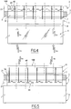
- Figure 4 and Figure 5 respectively show a first and a second photodetecting devices, comprising:
- the photosensitive layer 1 is made of monocrystalline semiconductor material, like Si, Si x Ge 1-x or some III-V or II-VI alloys.
- the photosensitive layer 1 acts as a photodiode, it has at least one electrical junction, and thus comprises doping elements whose nature and/or concentration suddenly changes in the thickness of the photosensitive layer 1.
- the photosensitive layer 1 can then be a PN-type junction, a PP + -type junction, a NN - -type junction, a PiN-type junction, or other type of junctions.
- the photosensitive layer 1 is preferably covered and underlied by electrode layers respectively 8 and 7, for biasing it.
- One electrode layer 8, located on the photoreceiving side of the photosensitive layer 1, has to be transparent to permit at least part of the photons to cross it, and thus to permit the underlying photosensitive layer 1 to receive them.
- This electrode layer 8 can be for instance made of ITO (Indium Tin Oxide).
- the other electrode layer 7 can be of any electrical conductive material, such as aluminium or TiW.
- the circuit layer 2 includes the whole electronic components that receive, and optionally amplify, switch and command electronical charges coming from the photosensitive layer 1.
- This circuit layer 2 has preferably two areas:
- Each photodetecting unit 100 (or pixels 100) comprises at least one electronic component 20 (illustrated in figures 4 and 5 as a transistor) and the part of the photosensitive layer 1 which is directly above the said at least electronic component 20.
- a via hole 40 being an electrically conductive channel.
- the via hole 40 can be for instance filled with Al or TiW, or other conductive materials.
- This via hole 40 allows to link the photosensitive layer 1 to the input of the at least electronic component 20 (illustrated in the figures 4 and 5 as the source of a transistor 20).
- a field isolation layer 3 separates the photosensitive layer 1 from the circuit layer 2, and comprises, at its peripheral part 31 a shielding whose function is the protection of the peripheral zone 21 of the circuit layer 2 (and the included addressing components) from the outside illumination.
- Material chosen for shielding may be all non transparent material at the considered wavelength, for instance tungsten or nickel.
- the central zone 32 of the isolation layer 3 electrically separates the circuit layer 2 from the photosensitive layer 1, except for the via holes 40 which passes through.
- the central zone 32 can be of a dielectric material, such as SiO 2 , Si 3 N 4 , Si x O y N z .
- the photodetecting device preferably comprises a holding substrate which mechanically stiffens the whole device.
- Figure 4 shows a first photodetecting device wherein the holding substrate 6 is located on the side of the photosensitive layer 1.
- this holding substrate 6 has to be made of a transparent material to photons, as glass or quartz or any other material transparent to the wavelength of interest.
- This first photodetecting device is then illuminated "by the back".
- Figure 5 shows a second photodetecting device manufactured by the method of the invention wherein the holding substrate 9 is located on the side of the circuit layer 2.
- the holding substrates 9 can be in any material, like a semiconductor material, as Si.
- This second photodetecting device is then illuminated "by the front”.
- Photodetecting device of the present invention does not necessary comprise a photosensitive layer 1 in an amorphous semiconductor material, but can comprise a photosensitive layer 1 of crystalline semiconductor material, even if the underlied layer (electrode layer 7 or 8 and/or isolation layer 3) is not of a crystalline material, contrary to the photodetecting device of the prior art wherein the photosensitive layer 1 has to be in an amorphous material because of the non possibility of growing a crystalline material from a non crystalline surface.
- the photodetecting device then improves the reliability and the efficiency of the photosensitive layer 1, as crystalline semiconductor material does not comprise any charge-traps like in an amorphous material, and consequently does not present problems of a low average number of electrons generated by incoming photons like in amorphous and then it leads to a more sensible detector.
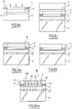
- Figure 6a to 6m show several steps of the method of manufacturing a photodetecting device in accordance with the invention (the said first photodetecting device referring to figure 4 ).
- a first step comprises providing a semiconductor substrate 5 on which the photosensitive layer 1 is grown, in order to make a donor substrate III.
- the first substrate 5 is preferably a monocristalline substrate which can be made of a bulk material (like Si or AsGa) or made of different sorts of materials like a first substrate 5 comprising a bulk substrate Si and a buffer structure (which confines plastic defaults and adapts the lattice parameter) in SiGe.
- a monocristalline substrate which can be made of a bulk material (like Si or AsGa) or made of different sorts of materials like a first substrate 5 comprising a bulk substrate Si and a buffer structure (which confines plastic defaults and adapts the lattice parameter) in SiGe.
- the first substrate 5 presents a top surface preferably monocrystalline with little plastic defaults.
- the photosensitive layer 1 is then grown by any known epitaxial techniques, such as CVD techniques, as PECVD, MOCVD, LEPCVD...
- the photosensitive layer 1 is formed by deposition in order to make a non crystalline photosensitive layer 1 like an amorphous structures.
- steps of doping succeeds to the growth step, such that the photosensitive layer 1 comprises at least two levels of doped zones, a doped zone having a doping element with different concentration and/or different nature from the other doped zones.
- the photosensitive layer 1 can present a PN junction, a NN-junction, a PP+ junction, a PiN junction...., depending on the requirement.
- a first electrode layer 8 is optionally formed on the photosensitive layer 1.
- This electrode layer 8 is made of a transparent conductive layer, such as ITO.
- an implanting step consists in implanting atomic species like hydrogen and/or helium ions, through the top surface of the donor substrate III, so as to create in the first substrate 5 an embrittlement zone 4.
- the concentration and the energy of the atomic species are chosen such that the embrittlement zone 4 is located in the first substrate 5 and presents some mechanical weakness comparing with the other part of the donor substrate III.
- a holding substrate 6 is provided and bonded to the donor substrate III.
- This holding substrate 6 is made of a material transparent to photons that the photodetecting device will receive, such as glass or quartz.
- the donor substrate III and/or the holding substrate 6 can be polished or cleaning in order to reduce the rugosity.
- the bonding can be realized by molecular adhesion, which is mainly due to hydrophily of the surfaces to be bonded.
- Preparation of the surface(s) to be bonded can be optionally done for improving the bonding energy between the holding substrate 6 and the donor substrate III, such as for example an exposition to a plasma (of oxygen for example), a cleaning, a brushing, ...
- the bonding interface can be optionally strengthened by a thermal treatment, at a low bonding temperature for instance 600°C-900°C for 1 hour.
- bonding could be assisted by a plasma activation.
- the first substrate 5 is reduced by bringing some energy at the embrittlement zone 4 in order to create a detachment of the major part of the first substrate 5.
- the energy provided can be for instance mechanical energy and/or thermal energy or other kind of energy.
- a first alternative of reduction of the first substrate 5 can also be processed, in which the formation of the embrittlement zone 4 is differently done than by implanting atomic species (as illustrated in figure 6c ), but by implementing, before the formation of the photosensitive layer 1 (referring to figure 6a ), the following steps :
- first substrate 5 also called “dismountable substrate”
- mountable substrate by controlling of the bonding energy, is described for example in the FR 2,823,599 document, the principle being based on a reduction of the bonding forces between the said two wafers bonded together, relative to an optimal bonding.
- a second alternative of reduction of the first substrate 5 is the etch-back technique (i.e. a chemical etching from the back of the first substrate 5).
- an optional second electrode layer 7 is formed on the photosensitive layer 1, this second electrode layer 7 being made of an electrically conductive material, such as Al, TiW.
- the technique for forming this second electrode 7 can be an electroplating.
- a second wafer II is formed by providing a second substrate 9, on which a circuit layer 2 is formed.
- the second substrate 9 is preferably made of a monocrystalline material such as bulk material like Si, or a composite substrate comprising for instance a buffer structure.
- an electronic circuit layer 2 On the second substrate 9, is formed an electronic circuit layer 2, such that a central part 22 includes the whole electronic components of the different pixels 100, and a peripheral part 21 including the electronic components dedicated to the addressing.
- the layout of the circuit layer 2 is chosen to process the electronic charges coming from the photosensitive layer 1 (which will next overly the circuit layer 2), choosing thus in consequence a circuit configuration and a path for the metallic tracks, inside the circuit layer 2.
- CMOS circuit can be manufactured in each pixel 100.
- a field isolation layer 3 is then formed on the circuit layer 2, this isolation layer 3 comprising a peripheral part 31 of shielding for protecting the underlied peripheral part 21 of the circuit layer 2, and a central part 32 which covers the central part 21 of the circuit layer 2.
- the shielding material chosen for the peripheral part 31 of the isolation layer 3 may be all non transparent material at the considered wavelength, for instance tungsten or nickel.
- the material chosen for the central part 32 of the isolation layer 3 is preferably made of a dielectric material, such as SiO 2 , Si 3 N 4 , Si x O y N z ,...
- This isolation layer 3 will then electrically separate the circuit layer 2 from the photosensitive layer 1 (which will next underly the isolation layer 3).
- implanting step is processed inside the second substrate 9 (like the implanting step in the substrate 5 described above, referring to figure 6c ) in order to create a second embrittlement zone 4' in the second substrate 9.
- the second wafer II and the first wafer I are then bonded.
- Some energy is provided in order to detach a major part of the second substrate 9, this energy can be mechanical energy, and/or thermal energy, or other kind of energy.
- the remaining part 9' of it is then removed by some technique of surface texture, such as polishing, selective etching, CMP, oxidation, thermal anneals.
- the photodetecting device is finally obtained by forming via holes from the surface of the circuit layer 2 to the photosensitive layer 1 (by technique of masks and etching through the non-masked surface of the circuit layer 2) and by filling them with an electrical conductive layer, such as Al, TiW, or another material, in order to create conductive vias 40 between the input of some electronic components included in the central part 22 of the circuit layer 2, and the photosensitive layer 1, forming thus the said first photodetecting device (referring to figure 4 ).
- an electrical conductive layer such as Al, TiW, or another material
- a first electrode layer 7 is formed on the photosensitive layer 1 (referring to figure 7b ).
- This first electrode layer 7 being non-transparent to photons (contrary to the first electrode layer 8 referring to figure 6b of the said method of manufacturing according to the invention).
- the first wafer I is directly bonded to the second wafer II for obtaining a structure comprising successively a circuit layer 2, a field isolation layer 3, an optional first electrode layer 7 and a photosensitive layer 1.
- this second method does not comprise steps of providing and bonding a transparent holding substrate 6 previously to the bonding between the first and second wafers I-II (referring to figure 6d ).
- via holes 40 are formed from the surface of the photosensitive layer 1 to inputs of some electronic components of the central part 22 of the photosensitive layer 2, passing through the optional first electrode layer 7 and the isolation layer 3 (with techniques similar to those used referring to figure 6m ).
- an optional second electrode layer 8 is formed on the photosensitive layer 1, with a transparent conductive material such as ITO, so that at least a part of the photons to be received can cross it.
- the said second detecting device (referring to figure 5 ) is then formed.
Landscapes
- Solid State Image Pick-Up Elements (AREA)
- Light Receiving Elements (AREA)
Description
- The invention relates to a manufacturing of a photodetecting device, comprising a photosensitive part and an electronic circuit part, such as a CMOS image sensor.
- Such a photodetecting device comprises a plurality of photodetecting units, also called pixels, which are usually arranged in rows and columns. Each of the photodetecting units comprises:
- a photosensitive part, like a photodiode, at its surface, able to convert the received photons to an electronic signal;
- at least one electronic part, like a transistor, electrically connected to the photosensitive part, able to process, once-having received a command "ON", the accumulated electronic charges coming from the latter to other components (amplificatory, switch, ...) to readout means (for more details, see for instance §2 and §3 of
EP 1,256,984 document). - One of the main advantages of this technology is the rapid readout of the light information, due to a light acquisition in parallel over the different units.
- Several kinds of structural configuration of photodetecting devices have been proposed.
- As disclosed for example in
US 6,380,5668 -
Figure 1a illustrates such apixel 100, having a photodiode 10 (composed here, for example, of a p-type layer 10a and a n-type layer 10b), able to convert the received photons (hv) in electronic charges and, beside, a transistor 20 (surrounded by a field isolation layer 30) able to receive the electronic charges from thephotodiode 10a. - As shown on
figure 1b , which represents a front view of thephotoreceivor pixel surface 100, the latter comprises aphotosensitive part 10 and anon-photosensitive part 25. - Typically, the photosensitive surface represents 30% to 60% of the entire pixel surface.
- Consequently, the photosensing is not optimised, since a part of the photons arriving on the pixel are lost.
- A solution would be to reduce the size of the
electronic part 20. - But such miniaturization has its own technical limits. Furthermore, even if the electronic part is drastically reduced in size, the surface of the
pixel 100, in such a horizontal configuration, will not be dedicated to photosensing by 100%. - It was proposed to add a lens over each pixel for focusing the entire light, arriving on the pixel, to the photosensitive element; as disclosed in the
US 6,040,591 document. - But this solution is not desirable, due to its high cost and to an efficiency not sufficient enough.
- A second kind of known photosensitive device is the so-called "back-illuminated" device.
-
Figure 2a illustrates this device which initially comprises a doped substrate (for instance a p+-type) covered by atop layer 1a having another type of doping (for instance a p--type), and an electronic circuit layer 2 (including a plurality of transistors 20). The substrate is then selectively back-etched, such as to preserve theperiphery 1b, and thus forming acentral opening 15. Theperiphery 1a of the substrate then holds a thin structure comprising thetop layer 1a and thecircuit layer 2. - This structure allows the
thin top layer 1a to receive the photons coming from the "back" (i.e. passing through the opening 15) and delivering an electronic signal associated with this photon illumination to thetransistors 20 included in theoverlying circuit layer 2. - From
Figures 2b and 2c , which represent respectively front views of the surface of apixel 100 and of the opposite surface, it appears that this device doesn't have the drawbacks of the said first photodetecting device, as thetransistor 20 is not on the photoreceiving surface, the latter being then close to 100 % dedicated to photosensing. - However, the manufacturing of this second photodetecting device is high cost and implies to lose an important part of the back substrate during the etch-back process.
- A third known photodetecting device has a vertical configuration, i.e. electronic part is buried under the photosensitive part, as disclosed for instance in
DE 198 38 442 C ,EP 1,256,984 ;EP 1,026,747 ;EP 964,570 US 5,084,747 . -
Figure 3 illustrates such photodetecting device which is fabricated from asubstrate 9 from which anelectronic circuit layer 2 is formed (by crystal growth, doping, plating, deposition,...). Thiscircuit layer 2 usually comprises a circuitcentral part 22 including thetransistors 20 of each pixel and aperipheral part 21 comprising electronic components dedicated to addressing (i.e. collecting the signals from the pixels and sending them to readout means). Thecircuit layer 2 is covered by anisolation layer 3, mainly of a dielectric material with ashielding 31 on the periphery for protecting theperipheral part 21 from illumination. Theisolation layer 3 comprises electrical conductor channels (not shown), so called "via hole", so as to electrically link the photosensitive part to the electronic part. A doped photosensitive layer 1 (for instance a PiN structure composed of a p-type layer 1a, anintrinsic layer 1b and a n-type layer 1c) is formed on theisolation layer 3. - Due to the non-crystallinity of the
isolation layer 3, a crystal growth of thephotosensitive layer 1 is not possible. So, thephotosensitive layer 1 is formed by deposition, and has an amorphous structure. - Now, an amorphous layer comprises many charges traps able to immobilise electrons and holes during a time, so called "time of relaxation". These trapped charges slow down the reception and interfere with the next detections.
- The average number of electrons generated by incoming photons is then lower for non crystalline layers, from which it follows a lower efficiency for this type of device and leads to a less sensible detector.
- The invention concerns a method of manufacturing a photodetecting device, comprising the steps of
claim 1. - the material chosen for the field isolation zone is a dielectric, such as SiO2, Si3N4 or SixOyNz;
- the step of removing substrate is operated by at least one of the following techniques : chemical etching, selective chemical etching, grinding , polishing, CMP;
- the step of removing substrate comprises an energy input for detaching the said substrate over an embrittlement zone previously formed in the said substrate;
- the method further comprises a formation of the said embrittlement zone in the said substrate by implantation of atomic species, such as hydrogen and/or helium;
- the method further comprises a formation of the said embrittlement zone by the following steps :
- ✔ providing a third and a fourth wafers;
- ✔ etching a surface of at least one of the third and the fourth wafers, in order to increase the surface roughness;
- ✔ bonding the third and the fourth wafers at the rough surface(s), forming thus the said substrate, the rough interface being the said embrittlement zone;
- the method further comprises a surface finishing step of the detached surface, employing at least one of the following techniques : selective chemical etching, polishing, CMP, oxidation, thermal anneals;
- the formation of the photosensitive layer on the first substrate comprises crystal growth and doping;
- the formation of the field isolation layer comprises the formation of a shielding to photons in periphery of the field isolation layer over a determinate width;
- the circuit layer comprises a plurality of transistors, and in that the circuit layer is patterned such that, once step (f) is implemented, parts of the photosensitive layer are electrically connected to some transistors by some conductive via, forming thus a plurality of photodetecting units (so-called pixels);
- the electronic components by pixel comprise CMOS component.
- Other characteristics, purposes and advantages of the invention will appear in the next detailed description of the invention, illustrated by the following drawings :
-
Figure 1a is a schematic cross-sectional view of a photodetecting device according to a first prior art. -
Figure 1b is a schematic front view of the surface, of the photodetecting device according to the first prior art, which detects photons. -
Figure 2a is a schematic cross-sectional view of a photodetecting device according to a second prior art. -
Figure 2b and 2c are respectively schematic front views of the surface of the photodectecting device according to the second prior art, which detects the photons and the opposite surface. -
Figure 3 is a schematic cross-sectional view of a photodetecting device according to a third prior art. -
Figure 4 is a schematic cross-sectional view of a first detecting device manufactured by the method of the invention. -
Figure 5 is a schematic cross-sectional view of a second photodetecting device not forming part of the present invention. -
Figure 6a to 6m are the different steps of a first method of manufacturing the first photodetecting device according to the invention. -
Figure 7a to 7h are different steps of a second method of manufacturing the second photodetecting device. - A first object of the invention is the manufacturing of a photodetecting device having vertical configuration, comprising a photosensitive layer made of a crystalline semiconductor material.
- A second object of the invention is to process a method of manufacturing such photodetecting device so that the photosensing surface is 100% dedicated or closed to 100% dedicated to the photosensing.
-
Figure 4 and Figure 5 respectively show a first and a second photodetecting devices, comprising: - a
photosensitive layer 1 ; - an
electronic circuit layer 2 ; - a
field isolation layer 3 separating thephotosensitive layer 1 and thecircuit layer 2. - Preferably, the
photosensitive layer 1 is made of monocrystalline semiconductor material, like Si, SixGe1-x or some III-V or II-VI alloys. - As the
photosensitive layer 1 acts as a photodiode, it has at least one electrical junction, and thus comprises doping elements whose nature and/or concentration suddenly changes in the thickness of thephotosensitive layer 1. - The
photosensitive layer 1 can then be a PN-type junction, a PP+-type junction, a NN--type junction, a PiN-type junction, or other type of junctions. - In order to facilitate or allow conversion of the received photons to electronic charges, the
photosensitive layer 1 is preferably covered and underlied by electrode layers respectively 8 and 7, for biasing it. - One
electrode layer 8, located on the photoreceiving side of thephotosensitive layer 1, has to be transparent to permit at least part of the photons to cross it, and thus to permit the underlyingphotosensitive layer 1 to receive them. - This
electrode layer 8 can be for instance made of ITO (Indium Tin Oxide). - The
other electrode layer 7 can be of any electrical conductive material, such as aluminium or TiW. - The
circuit layer 2 includes the whole electronic components that receive, and optionally amplify, switch and command electronical charges coming from thephotosensitive layer 1. - This
circuit layer 2 has preferably two areas: - a
central zone 22 which includes electronic components of thepixels 100, - a
peripheral zone 21 which includes the electronic components dedicated to the addressing process of the different pixels electronic components located in thecentral zone 22. - Each photodetecting unit 100 (or pixels 100) comprises at least one electronic component 20 (illustrated in
figures 4 and 5 as a transistor) and the part of thephotosensitive layer 1 which is directly above the said at leastelectronic component 20. - In a
pixel 100, the part ofphotosensitive layer 1 and the at leastelectronic component 20 are electronically linked by a viahole 40, a viahole 40 being an electrically conductive channel. - The via
hole 40 can be for instance filled with Al or TiW, or other conductive materials. - This via
hole 40 allows to link thephotosensitive layer 1 to the input of the at least electronic component 20 (illustrated in thefigures 4 and 5 as the source of a transistor 20). - A
field isolation layer 3 separates thephotosensitive layer 1 from thecircuit layer 2, and comprises, at its peripheral part 31 a shielding whose function is the protection of theperipheral zone 21 of the circuit layer 2 (and the included addressing components) from the outside illumination. Material chosen for shielding may be all non transparent material at the considered wavelength, for instance tungsten or nickel. - The
central zone 32 of theisolation layer 3 electrically separates thecircuit layer 2 from thephotosensitive layer 1, except for the via holes 40 which passes through. - The
central zone 32 can be of a dielectric material, such as SiO2, Si3N4, SixOyNz. - Further to the three preceding layers (i.e.
photosensitive layer 1,circuit layer 2 and isolation layer 3), the photodetecting device preferably comprises a holding substrate which mechanically stiffens the whole device. -
Figure 4 shows a first photodetecting device wherein the holdingsubstrate 6 is located on the side of thephotosensitive layer 1. - For allowing the photons to reach the
photosensitive layer 1, this holdingsubstrate 6 has to be made of a transparent material to photons, as glass or quartz or any other material transparent to the wavelength of interest. - This first photodetecting device is then illuminated "by the back".
- Furthermore, it allows electrical contacts directly to the
electronic components 20 of the uncoveredcircuit layer 2. -
Figure 5 shows a second photodetecting device manufactured by the method of the invention wherein the holdingsubstrate 9 is located on the side of thecircuit layer 2. - The holding
substrates 9 can be in any material, like a semiconductor material, as Si. - This second photodetecting device is then illuminated "by the front".
- Photodetecting device of the present invention does not necessary comprise a
photosensitive layer 1 in an amorphous semiconductor material, but can comprise aphotosensitive layer 1 of crystalline semiconductor material, even if the underlied layer (electrode layer photosensitive layer 1 has to be in an amorphous material because of the non possibility of growing a crystalline material from a non crystalline surface. - The photodetecting device according to the invention then improves the reliability and the efficiency of the
photosensitive layer 1, as crystalline semiconductor material does not comprise any charge-traps like in an amorphous material, and consequently does not present problems of a low average number of electrons generated by incoming photons like in amorphous and then it leads to a more sensible detector. -
Figure 6a to 6m show several steps of the method of manufacturing a photodetecting device in accordance with the invention (the said first photodetecting device referring tofigure 4 ). - Referring to
figure 6a , a first step comprises providing asemiconductor substrate 5 on which thephotosensitive layer 1 is grown, in order to make a donor substrate III. - The
first substrate 5 is preferably a monocristalline substrate which can be made of a bulk material (like Si or AsGa) or made of different sorts of materials like afirst substrate 5 comprising a bulk substrate Si and a buffer structure (which confines plastic defaults and adapts the lattice parameter) in SiGe. - In any case, the
first substrate 5 presents a top surface preferably monocrystalline with little plastic defaults. - The
photosensitive layer 1 is then grown by any known epitaxial techniques, such as CVD techniques, as PECVD, MOCVD, LEPCVD... - In a variant, the
photosensitive layer 1 is formed by deposition in order to make a non crystallinephotosensitive layer 1 like an amorphous structures. - In order to create the electrical junction in the
photosensitive layer 1, steps of doping succeeds to the growth step, such that thephotosensitive layer 1 comprises at least two levels of doped zones, a doped zone having a doping element with different concentration and/or different nature from the other doped zones. - Thus, the
photosensitive layer 1 can present a PN junction, a NN-junction, a PP+ junction, a PiN junction...., depending on the requirement. - Referring to
figure 6b , afirst electrode layer 8 is optionally formed on thephotosensitive layer 1. Thiselectrode layer 8 is made of a transparent conductive layer, such as ITO. - Referring to
figure 6c , an implanting step consists in implanting atomic species like hydrogen and/or helium ions, through the top surface of the donor substrate III, so as to create in thefirst substrate 5 anembrittlement zone 4. - The concentration and the energy of the atomic species are chosen such that the
embrittlement zone 4 is located in thefirst substrate 5 and presents some mechanical weakness comparing with the other part of the donor substrate III. - Referring to
figure 6d , a holdingsubstrate 6 is provided and bonded to the donor substrate III. - This holding
substrate 6 is made of a material transparent to photons that the photodetecting device will receive, such as glass or quartz. - Before bonding, the donor substrate III and/or the holding
substrate 6 can be polished or cleaning in order to reduce the rugosity. - The bonding can be realized by molecular adhesion, which is mainly due to hydrophily of the surfaces to be bonded.
- Preparation of the surface(s) to be bonded can be optionally done for improving the bonding energy between the holding
substrate 6 and the donor substrate III, such as for example an exposition to a plasma (of oxygen for example), a cleaning, a brushing, ... - For further details of the technique of bonding that can be used, the book "semiconductor wafer bonding science and technology" of Q-Y Tung and U. Gösele (a Wiley Interscience publication, Johnson Wiley and Sons, Inc.) can be read.
- The bonding interface can be optionally strengthened by a thermal treatment, at a low bonding temperature for instance 600°C-900°C for 1 hour. In addition, bonding could be assisted by a plasma activation.
- Referring to
figure 6e , thefirst substrate 5 is reduced by bringing some energy at theembrittlement zone 4 in order to create a detachment of the major part of thefirst substrate 5. - The energy provided can be for instance mechanical energy and/or thermal energy or other kind of energy.
- A first alternative of reduction of the
first substrate 5 can also be processed, in which the formation of theembrittlement zone 4 is differently done than by implanting atomic species (as illustrated infigure 6c ), but by implementing, before the formation of the photosensitive layer 1 (referring tofigure 6a ), the following steps : - providing two wafers,
- etching a surface of at least one of the two wafers, in order to increase the surface roughness,
- bonding the two wafers;
- The fabrication of such a
first substrate 5, also called "dismountable substrate", by controlling of the bonding energy, is described for example in theFR 2,823,599 - Then the detaching of the major part of the
first subtrate 5 is substantially processed as above-described referring tofigure 6d . - A second alternative of reduction of the
first substrate 5 is the etch-back technique (i.e. a chemical etching from the back of the first substrate 5). - Whatever techniques of reduction of the
first substrate 5 used, after having reduced thefirst substrate 5, a remaining part 5' of thefirst substrate 5 stays (referring tofigure 6e ) and is removed by mainly finition means as polishing, selective etching, CMP, oxidation... in order to obtain a structure composed of the holdingstructure 6, the optional transparentfirst electrode layer 8, and thephotosensitive layer 1, as shown infigure 6f . - Referring to
figure 6g , an optionalsecond electrode layer 7 is formed on thephotosensitive layer 1, thissecond electrode layer 7 being made of an electrically conductive material, such as Al, TiW. - The technique for forming this
second electrode 7 can be an electroplating. - Referring to
figure 6h , a second wafer II is formed by providing asecond substrate 9, on which acircuit layer 2 is formed. - The
second substrate 9 is preferably made of a monocrystalline material such as bulk material like Si, or a composite substrate comprising for instance a buffer structure. - On the
second substrate 9, is formed anelectronic circuit layer 2, such that acentral part 22 includes the whole electronic components of thedifferent pixels 100, and aperipheral part 21 including the electronic components dedicated to the addressing. - Techniques employed for manufacturing those components are conventional ones, as for instance epitaxy, doping, depositing, electro plating...
- The layout of the
circuit layer 2 is chosen to process the electronic charges coming from the photosensitive layer 1 (which will next overly the circuit layer 2), choosing thus in consequence a circuit configuration and a path for the metallic tracks, inside thecircuit layer 2. - For example, a CMOS circuit can be manufactured in each
pixel 100. - A
field isolation layer 3 is then formed on thecircuit layer 2, thisisolation layer 3 comprising aperipheral part 31 of shielding for protecting the underliedperipheral part 21 of thecircuit layer 2, and acentral part 32 which covers thecentral part 21 of thecircuit layer 2. - The shielding material chosen for the
peripheral part 31 of theisolation layer 3 may be all non transparent material at the considered wavelength, for instance tungsten or nickel. - The material chosen for the
central part 32 of theisolation layer 3 is preferably made of a dielectric material, such as SiO2, Si3N4, SixOyNz,... - This
isolation layer 3 will then electrically separate thecircuit layer 2 from the photosensitive layer 1 (which will next underly the isolation layer 3). - Referring to
figure 6i , implanting step is processed inside the second substrate 9 (like the implanting step in thesubstrate 5 described above, referring tofigure 6c ) in order to create a second embrittlement zone 4' in thesecond substrate 9. - Referring to
figure 6j , the second wafer II and the first wafer I are then bonded. - The technique of bonding used for this step is similar to the technique of bonding used during step referring to
figure 6d (and described above). - Some energy is provided in order to detach a major part of the
second substrate 9, this energy can be mechanical energy, and/or thermal energy, or other kind of energy. - The above-mentioned two other alternatives for the reduction of the
first substrate 5, can also be adapted to the reduction of thesecond substrate 9. - Referring to
figure 6k and 6l , after having reduced thesecond substrate 9, the remaining part 9' of it is then removed by some technique of surface finition, such as polishing, selective etching, CMP, oxidation, thermal anneals. - Referring to
figure 6m , the photodetecting device is finally obtained by forming via holes from the surface of thecircuit layer 2 to the photosensitive layer 1 (by technique of masks and etching through the non-masked surface of the circuit layer 2) and by filling them with an electrical conductive layer, such as Al, TiW, or another material, in order to createconductive vias 40 between the input of some electronic components included in thecentral part 22 of thecircuit layer 2, and thephotosensitive layer 1, forming thus the said first photodetecting device (referring tofigure 4 ). - Referring to
figure 7a to 7h , a second method of manufacturing a photodetecting device (for obtaining the said second photodetecting device referring tofigure 5 ), is proposed, which does not form part of the invention. - After having formed the
photosensitive layer 1 and a first substrate 5 (referring tofigure 7a ) in order to form a first wafer I, afirst electrode layer 7 is formed on the photosensitive layer 1 (referring tofigure 7b ). - This
first electrode layer 7 being non-transparent to photons (contrary to thefirst electrode layer 8 referring tofigure 6b of the said method of manufacturing according to the invention). - After having implanting atomic species in the first wafer I and having formed a second wafer II including a holding
substrate 9, acircuit layer 2 and a field isolation layer 3 (with techniques substantially and respectively similar to those above-described referring tofigure 6c and figure 6h ). - Then, referring to
figure 7e , the first wafer I is directly bonded to the second wafer II for obtaining a structure comprising successively acircuit layer 2, afield isolation layer 3, an optionalfirst electrode layer 7 and aphotosensitive layer 1. - It is noticed that, contrary to the said first method of manufacturing a photodetecting device, this second method does not comprise steps of providing and bonding a
transparent holding substrate 6 previously to the bonding between the first and second wafers I-II (referring tofigure 6d ). - After having reduced the first substrate 5 (with the same technique as above described referring to
figure 6c and figure 6d or, with one of the said alternative techniques as above-described for the said first method of manufacturing a photodetecting device), and having removed the remaining part 5' of thefirst substrate 5, viaholes 40 are formed from the surface of thephotosensitive layer 1 to inputs of some electronic components of thecentral part 22 of thephotosensitive layer 2, passing through the optionalfirst electrode layer 7 and the isolation layer 3 (with techniques similar to those used referring tofigure 6m ). - Referring to
figure 7h , an optionalsecond electrode layer 8 is formed on thephotosensitive layer 1, with a transparent conductive material such as ITO, so that at least a part of the photons to be received can cross it. - The said second detecting device (referring to
figure 5 ) is then formed.
Claims (13)
- Method of manufacturing a photodetecting device, comprising sequentially the following steps:(a) providing a first wafer (I) comprising the following steps:- forming a photosensitive layer (1) made of a material chosen from semiconductor materials, on a first substrate (5);- forming a first electrode layer (8) made of a transparent electrical conductive material, such as ITO, on the photosensitive layer (1);- bonding the photosensitive layer having the first electrode layer (8) thereon with a holding substrate (6) made of a transparent material, such as quartz or glass from the photosensitve side of the photosensitive layer (1);- removing the first substrate (5);- forming a second electrode layer (7) made of an electrical conductive material on the photosensitive layer (1);(b) providing a second wafer (II) by forming a circuit layer (2) including electronic components on a second substrate (9),(c) forming a field isolation layer (3) covering the second electrode layer (7) or the circuit layer (2);(d) bonding the first wafer (I) and the second wafer (II) so as to form a structure comprising successively the circuit layer (2), the field isolation layer (3), the second electrode layer (7), the photosensitive layer (1), the first electrode layer (8) and the holding substrate (6);(e) removing the said second substrate (9);(f) forming electrically conductive via (40) so as to electrically connect the photosensitive layer (1) to inputs of some electronic components of the circuit layer (2).
- Method of manufacturing a photodetecting device according to the previous claim, in which step (d) comprises a molecular adhesion.
- Method of manufacturing a photodetecting device according to the previous claim, in which step (d) comprises, after the molecular adhesion, a thermal treatment, at least one of the materials which constitutes the field isolation zone (3) is SiO2, Si3N4 or SixOyNz being chosen for improving the bonding when this thermal treatment is processed.
- Method of manufacturing a photodetecting device according to one of the previous claims, in which the step of removing the first or second substrate is realized by at least one of the following techniques: chemical etching, selective chemical etching, grinding, polishing, CMP.
- Method of manufacturing a photodetecting device according to one of the previous claims, in which the step of removing the first or second substrate comprises an energy input for detaching the said substrate (5, 9) over an embrittlement zone (4,4') previously formed in the said substrate (5, 9).
- Method of manufacturing a photodetecting device according to the previous claim, further comprising a formation of the said embrittlement zone (4, 4') in the said substrate (5, 9) by implantation of atomic species, such as hydrogen and/or helium.
- Method of manufacturing a photodetecting device according to claim 5, further comprising a formation of the said embrittlement zone (4, 4') by the following steps:- providing a third and a fourth wafers;- etching a surface of at least one of the third and the fourth wafers, in order to increase the surface roughness;- bonding the third and the fourth wafers at the rough surface(s), forming thus the said first or second substrate (5, 9), the rough interface being the said embrittlement zone (4, 4').
- Method of manufacturing a photodetecting device according to one of the three previous claims, further comprising a surface finishing step of the detached surface (5', 9'), employing at least one of the following techniques : selective chemical etching, polishing, CMP, oxidation, thermal anneals.
- Method of manufacturing a photodetecting device according to claim 1, in which the formation of the photosensitive layer (1) on the first substrate (5) comprises crystal growth and doping.
- Method of manufacturing a photodetecting device according to one of the two previous claims, in which the via holes are formed during step (f) through the surface of the circuit layer (2), from inputs of some electronic components of the circuit layer (2) to the photosensitive layer (1).
- Method of manufacturing a photodetecting device according to one of the previous claims, in which the formation of the field isolation layer (3) according to step (c) comprises the formation of a shielding to photons in periphery of the field isolation layer (3) over a determinate width.
- Method of manufacturing a photodetecting device according to one of the previous claims, in which the circuit layer (2) comprises a plurality of transistors (20), and in that the circuit layer (2) is patterned such that, once step (f) is implemented, parts of the photosensitive layer (1) are electrically connected to some transistors by some conductive via, forming thus a plurality of photodetecting units (100), also called pixels (100).
- Method of manufacturing a photodetecting device according to the previous claim, in which the electronic components (20) in the pixels (100) comprise CMOS components.
Priority Applications (1)
| Application Number | Priority Date | Filing Date | Title |
|---|---|---|---|
| EP10174657.6A EP2249389B1 (en) | 2004-02-25 | 2004-02-25 | Method of manufacturing a photodetecting device |
Applications Claiming Priority (1)
| Application Number | Priority Date | Filing Date | Title |
|---|---|---|---|
| PCT/IB2004/000905 WO2005086236A1 (en) | 2004-02-25 | 2004-02-25 | Photodetecting device |
Related Child Applications (2)
| Application Number | Title | Priority Date | Filing Date |
|---|---|---|---|
| EP10174657.6A Division-Into EP2249389B1 (en) | 2004-02-25 | 2004-02-25 | Method of manufacturing a photodetecting device |
| EP10174657.6A Division EP2249389B1 (en) | 2004-02-25 | 2004-02-25 | Method of manufacturing a photodetecting device |
Publications (2)
| Publication Number | Publication Date |
|---|---|
| EP1719179A1 EP1719179A1 (en) | 2006-11-08 |
| EP1719179B1 true EP1719179B1 (en) | 2018-10-03 |
Family
ID=34917498
Family Applications (1)
| Application Number | Title | Priority Date | Filing Date |
|---|---|---|---|
| EP04714396.1A Expired - Lifetime EP1719179B1 (en) | 2004-02-25 | 2004-02-25 | Photodetecting device |
Country Status (6)
| Country | Link |
|---|---|
| US (2) | US7452745B2 (en) |
| EP (1) | EP1719179B1 (en) |
| JP (1) | JP5054509B2 (en) |
| KR (1) | KR100938866B1 (en) |
| CN (1) | CN1922732B (en) |
| WO (1) | WO2005086236A1 (en) |
Families Citing this family (33)
| Publication number | Priority date | Publication date | Assignee | Title |
|---|---|---|---|---|
| FR2864336B1 (en) * | 2003-12-23 | 2006-04-28 | Commissariat Energie Atomique | METHOD FOR SEALING TWO PLATES WITH FORMATION OF AN OHMIC CONTACT BETWEEN THEM |
| EP1719179B1 (en) * | 2004-02-25 | 2018-10-03 | Sony Semiconductor Solutions Corporation | Photodetecting device |
| EP2249389B1 (en) * | 2004-02-25 | 2019-02-20 | Sony Semiconductor Solutions Corporation | Method of manufacturing a photodetecting device |
| FR2872627B1 (en) * | 2004-06-30 | 2006-08-18 | Commissariat Energie Atomique | MOLECULAR ADHESION ASSEMBLY OF TWO SUBSTRATES |
| FR2888400B1 (en) * | 2005-07-08 | 2007-10-19 | Soitec Silicon On Insulator | LAYER TAKING METHOD |
| KR100798276B1 (en) | 2006-08-23 | 2008-01-24 | 동부일렉트로닉스 주식회사 | Image sensor and its manufacturing method |
| KR100872719B1 (en) | 2007-04-17 | 2008-12-05 | 동부일렉트로닉스 주식회사 | Image sensor and manufacturing method thereof |
| US7687836B2 (en) * | 2007-05-24 | 2010-03-30 | Micron Technology, Inc. | Capacitance noise shielding plane for imager sensor devices |
| JP5142831B2 (en) * | 2007-06-14 | 2013-02-13 | 株式会社半導体エネルギー研究所 | Semiconductor device and manufacturing method thereof |
| JP2009065160A (en) * | 2007-09-06 | 2009-03-26 | Dongbu Hitek Co Ltd | Image sensor and manufacturing method thereof |
| JP2009065156A (en) * | 2007-09-06 | 2009-03-26 | Dongbu Hitek Co Ltd | Manufacturing method of image sensor |
| KR100863361B1 (en) * | 2007-09-07 | 2008-10-13 | 주식회사 동부하이텍 | Image sensor and manufacturing method |
| KR100849238B1 (en) * | 2007-09-07 | 2008-07-29 | 주식회사 동부하이텍 | Image sensor and manufacturing method |
| JP2009065161A (en) * | 2007-09-07 | 2009-03-26 | Dongbu Hitek Co Ltd | Image sensor and manufacturing method thereof |
| KR100997299B1 (en) * | 2007-09-07 | 2010-11-29 | 주식회사 동부하이텍 | Image sensor and manufacturing method |
| DE102008046030A1 (en) | 2007-09-07 | 2009-06-10 | Dongbu Hitek Co., Ltd. | Image sensor and method for its production |
| DE102008046036A1 (en) * | 2007-09-07 | 2009-04-16 | Dongbu Hitek Co., Ltd. | Image sensor and method for its production |
| KR100882980B1 (en) * | 2007-09-07 | 2009-02-12 | 주식회사 동부하이텍 | Image sensor and its manufacturing method |
| KR100882979B1 (en) * | 2007-09-07 | 2009-02-12 | 주식회사 동부하이텍 | Image sensor and manufacturing method |
| KR100860141B1 (en) * | 2007-09-10 | 2008-09-24 | 주식회사 동부하이텍 | Image sensor and manufacturing method |
| KR100855403B1 (en) * | 2007-11-27 | 2008-08-29 | 주식회사 동부하이텍 | Image sensor and manufacturing method |
| KR100855404B1 (en) * | 2007-12-21 | 2008-08-29 | 주식회사 동부하이텍 | Image sensor and manufacturing method |
| KR100882987B1 (en) * | 2008-06-13 | 2009-02-12 | 주식회사 동부하이텍 | Image sensor and manufacturing method |
| KR101030299B1 (en) * | 2008-08-08 | 2011-04-20 | 주식회사 동부하이텍 | Semiconductor element and manufacturing method thereof |
| KR101024770B1 (en) * | 2008-09-30 | 2011-03-24 | 주식회사 동부하이텍 | Image sensor and manufacturing method |
| KR20100037211A (en) * | 2008-10-01 | 2010-04-09 | 주식회사 동부하이텍 | Image sensor and method for fabricating the same |
| KR101033353B1 (en) * | 2008-10-14 | 2011-05-09 | 주식회사 동부하이텍 | Image sensor and manufacturing method |
| GB0821158D0 (en) * | 2008-11-20 | 2008-12-24 | Durham Scient Crystals Ltd | Semiconductor device connection |
| JP4835710B2 (en) * | 2009-03-17 | 2011-12-14 | ソニー株式会社 | Solid-state imaging device, method for manufacturing solid-state imaging device, driving method for solid-state imaging device, and electronic apparatus |
| WO2014054586A1 (en) | 2012-10-02 | 2014-04-10 | 独立行政法人科学技術振興機構 | Signal detection device and signal detection method |
| FR3053838B1 (en) | 2016-07-08 | 2018-08-17 | Thales | METHOD FOR MANUFACTURING A PHOTODETECTOR COMPRISING A STACK OF SUPERIMPOSED LAYERS |
| FR3076292B1 (en) * | 2017-12-28 | 2020-01-03 | Commissariat A L'energie Atomique Et Aux Energies Alternatives | METHOD FOR TRANSFERRING A USEFUL LAYER ONTO A SUPPORT SUBSTRATE |
| CN121398176B (en) * | 2025-12-23 | 2026-04-21 | 合肥晶合集成电路股份有限公司 | Backside illuminated image sensor and preparation method thereof |
Family Cites Families (33)
| Publication number | Priority date | Publication date | Assignee | Title |
|---|---|---|---|---|
| DE3544182A1 (en) * | 1985-12-13 | 1987-06-19 | Heimann Gmbh | CONTACT IMAGE SENSOR LINE |
| JPH02275670A (en) | 1989-01-18 | 1990-11-09 | Canon Inc | Photoelectric converter and image reader |
| JP2617798B2 (en) * | 1989-09-22 | 1997-06-04 | 三菱電機株式会社 | Stacked semiconductor device and method of manufacturing the same |
| US5633526A (en) * | 1992-11-01 | 1997-05-27 | Rohm Co., Ltd. | Photodiode array and method for manufacturing the same |
| US5895274A (en) | 1996-01-22 | 1999-04-20 | Micron Technology, Inc. | High-pressure anneal process for integrated circuits |
| US5808329A (en) * | 1996-07-15 | 1998-09-15 | Raytheon Company | Low light level imager with extended wavelength response employing atomic bonded (fused) semiconductor materials |
| JPH10270672A (en) | 1997-03-25 | 1998-10-09 | Sony Corp | Solid-state imaging device |
| JP4200545B2 (en) | 1998-06-08 | 2008-12-24 | ソニー株式会社 | Solid-state imaging device, driving method thereof, and camera system |
| JP4273540B2 (en) | 1998-07-21 | 2009-06-03 | 株式会社Sumco | Bonded semiconductor substrate and manufacturing method thereof |
| DE19838442C1 (en) * | 1998-08-24 | 2000-03-02 | Fraunhofer Ges Forschung | Photodetector, especially a photodiode array useful for optical data storage and transmission, image processing, pattern recognition and spectrometry, is produced by back face bonding of a thinned photodetector wafer to a contact substrate |
| JP3600028B2 (en) * | 1998-08-24 | 2004-12-08 | シャープ株式会社 | X-ray image detector and method of manufacturing the same |
| US6944465B2 (en) | 1998-09-22 | 2005-09-13 | Polaris Wireless, Inc. | Estimating the location of a mobile unit based on the elimination of improbable locations |
| US5936261A (en) | 1998-11-18 | 1999-08-10 | Hewlett-Packard Company | Elevated image sensor array which includes isolation between the image sensors and a unique interconnection |
| US6328796B1 (en) | 1999-02-01 | 2001-12-11 | The United States Of America As Represented By The Secretary Of The Navy | Single-crystal material on non-single-crystalline substrate |
| US6252218B1 (en) | 1999-02-02 | 2001-06-26 | Agilent Technologies, Inc | Amorphous silicon active pixel sensor with rectangular readout layer in a hexagonal grid layout |
| US6358866B1 (en) | 1999-05-14 | 2002-03-19 | Imec Vzw | Method for post-oxidation heating of a structure comprising SiO2 |
| KR100384836B1 (en) | 1999-06-28 | 2003-05-22 | 주식회사 하이닉스반도체 | Image sensor and method for fabricating the same |
| US6204205B1 (en) | 1999-07-06 | 2001-03-20 | Taiwan Semiconductor Manufacturing Company | Using H2anneal to improve the electrical characteristics of gate oxide |
| US6309968B1 (en) | 1999-09-07 | 2001-10-30 | Vanguard International Semiconductor Corporation | Method to improve intrinsic refresh time and dichlorosilane formed gate oxide reliability |
| US6292529B1 (en) * | 1999-12-15 | 2001-09-18 | Analogic Corporation | Two-dimensional X-ray detector array for CT applications |
| JP2001267592A (en) * | 2000-03-14 | 2001-09-28 | Nikon Corp | Method of manufacturing semiconductor device, method of manufacturing back illuminated light receiving device, semiconductor device, and back illuminated light receiving device |
| FR2823599B1 (en) | 2001-04-13 | 2004-12-17 | Commissariat Energie Atomique | DEMOMTABLE SUBSTRATE WITH CONTROLLED MECHANICAL HOLDING AND METHOD OF MAKING |
| JP3719947B2 (en) * | 2001-04-18 | 2005-11-24 | シャープ株式会社 | Solid-state imaging device and manufacturing method thereof |
| FR2824664A1 (en) | 2001-05-09 | 2002-11-15 | St Microelectronics Sa | CMOS PHOTODETECTOR COMPRISING AN AMORPHOUS SILICON PHOTODIODE |
| JP4525958B2 (en) | 2001-08-27 | 2010-08-18 | 独立行政法人産業技術総合研究所 | Manufacturing method of semiconductor device |
| US6821873B2 (en) | 2002-01-10 | 2004-11-23 | Texas Instruments Incorporated | Anneal sequence for high-κ film property optimization |
| US6649538B1 (en) | 2002-10-09 | 2003-11-18 | Taiwan Semiconductor Manufacturing Co. Ltd. | Method for plasma treating and plasma nitriding gate oxides |
| JP4407127B2 (en) | 2003-01-10 | 2010-02-03 | 信越半導体株式会社 | Manufacturing method of SOI wafer |
| KR100947815B1 (en) | 2003-02-19 | 2010-03-15 | 신에쯔 한도타이 가부시키가이샤 | Manufacturing Method of SOI Wafer and SOI Wafer |
| EP1719179B1 (en) * | 2004-02-25 | 2018-10-03 | Sony Semiconductor Solutions Corporation | Photodetecting device |
| JP4631347B2 (en) | 2004-08-06 | 2011-02-16 | 株式会社Sumco | Partial SOI substrate and manufacturing method thereof |
| JP4830290B2 (en) | 2004-11-30 | 2011-12-07 | 信越半導体株式会社 | Manufacturing method of directly bonded wafer |
| US8138061B2 (en) | 2005-01-07 | 2012-03-20 | International Business Machines Corporation | Quasi-hydrophobic Si-Si wafer bonding using hydrophilic Si surfaces and dissolution of interfacial bonding oxide |
-
2004
- 2004-02-25 EP EP04714396.1A patent/EP1719179B1/en not_active Expired - Lifetime
- 2004-02-25 JP JP2007500305A patent/JP5054509B2/en not_active Expired - Fee Related
- 2004-02-25 CN CN2004800421325A patent/CN1922732B/en not_active Expired - Fee Related
- 2004-02-25 WO PCT/IB2004/000905 patent/WO2005086236A1/en not_active Ceased
- 2004-02-25 KR KR1020087030635A patent/KR100938866B1/en not_active Expired - Fee Related
-
2006
- 2006-08-24 US US11/510,870 patent/US7452745B2/en not_active Expired - Lifetime
-
2008
- 2008-07-31 US US12/183,538 patent/US7695996B2/en not_active Expired - Lifetime
Non-Patent Citations (1)
| Title |
|---|
| None * |
Also Published As
| Publication number | Publication date |
|---|---|
| KR100938866B1 (en) | 2010-01-27 |
| KR20090014211A (en) | 2009-02-06 |
| CN1922732B (en) | 2010-06-09 |
| CN1922732A (en) | 2007-02-28 |
| EP1719179A1 (en) | 2006-11-08 |
| JP2007524251A (en) | 2007-08-23 |
| US20080303113A1 (en) | 2008-12-11 |
| US20070018266A1 (en) | 2007-01-25 |
| US7695996B2 (en) | 2010-04-13 |
| US7452745B2 (en) | 2008-11-18 |
| JP5054509B2 (en) | 2012-10-24 |
| WO2005086236A1 (en) | 2005-09-15 |
Similar Documents
| Publication | Publication Date | Title |
|---|---|---|
| US7695996B2 (en) | Photodetecting device | |
| KR100888684B1 (en) | Photodetector | |
| US6984816B2 (en) | Vertically integrated photosensor for CMOS imagers | |
| US6927432B2 (en) | Vertically integrated photosensor for CMOS imagers | |
| US6809008B1 (en) | Integrated photosensor for CMOS imagers | |
| KR100889365B1 (en) | 3D image sensor and its manufacturing method | |
| US7214999B2 (en) | Integrated photoserver for CMOS imagers | |
| KR101594927B1 (en) | Back-illuminated cmos image sensors | |
| US9142585B2 (en) | Image sensor comprising isolated germanium photodetectors integrated with a silicon substrate and silicon circuitry | |
| US7932575B2 (en) | Method of fabricating back-illuminated imaging sensors using a bump bonding technique | |
| US5670817A (en) | Monolithic-hybrid radiation detector/readout | |
| KR20090057435A (en) | Image sensor using thin film SOI | |
| EP1685701B1 (en) | Image sensor comprising isolated germanium photodetectors integrated with a silicon substrate and silicon circuitry | |
| US5236871A (en) | Method for producing a hybridization of detector array and integrated circuit for readout | |
| US20050121707A1 (en) | Solid-state image sensing apparatus and method of manufacturing the same | |
| WO1994017557A1 (en) | Thermally matched readout/detector assembly and method for fabricating same | |
| EP2249389B1 (en) | Method of manufacturing a photodetecting device | |
| JP2008504707A (en) | Method for assembling two substrates using molecular bonds | |
| WO2006043105A1 (en) | Electro-optical device | |
| FR2887076A1 (en) | IMAGINE SEMICONDUCTOR SUBSTRATE IMAGE SENSOR WITH REAR METALLIZATION | |
| JPH05315580A (en) | Semiconductor photodetector and manufacture thereof |
Legal Events
| Date | Code | Title | Description |
|---|---|---|---|
| PUAI | Public reference made under article 153(3) epc to a published international application that has entered the european phase |
Free format text: ORIGINAL CODE: 0009012 |
|
| 17P | Request for examination filed |
Effective date: 20060816 |
|
| AK | Designated contracting states |
Kind code of ref document: A1 Designated state(s): AT BE BG CH CY CZ DE DK EE ES FI FR GB GR HU IE IT LI LU MC NL PT RO SE SI SK TR |
|
| RIN1 | Information on inventor provided before grant (corrected) |
Inventor name: CAYREFOURCQ, IAN Inventor name: DUPONT, FREDERIC |
|
| 17Q | First examination report despatched |
Effective date: 20061228 |
|
| DAX | Request for extension of the european patent (deleted) | ||
| RAP1 | Party data changed (applicant data changed or rights of an application transferred) |
Owner name: SOITEC |
|
| STAA | Information on the status of an ep patent application or granted ep patent |
Free format text: STATUS: EXAMINATION IS IN PROGRESS |
|
| RAP1 | Party data changed (applicant data changed or rights of an application transferred) |
Owner name: SONY SEMICONDUCTOR SOLUTIONS CORPORATION |
|
| RIC1 | Information provided on ipc code assigned before grant |
Ipc: H01L 27/146 20060101AFI20180223BHEP |
|
| GRAP | Despatch of communication of intention to grant a patent |
Free format text: ORIGINAL CODE: EPIDOSNIGR1 |
|
| STAA | Information on the status of an ep patent application or granted ep patent |
Free format text: STATUS: GRANT OF PATENT IS INTENDED |
|
| INTG | Intention to grant announced |
Effective date: 20180419 |
|
| RIN1 | Information on inventor provided before grant (corrected) |
Inventor name: DUPONT, FREDERIC Inventor name: CAYREFOURCQ, IAN |
|
| GRAS | Grant fee paid |
Free format text: ORIGINAL CODE: EPIDOSNIGR3 |
|
| GRAA | (expected) grant |
Free format text: ORIGINAL CODE: 0009210 |
|
| STAA | Information on the status of an ep patent application or granted ep patent |
Free format text: STATUS: THE PATENT HAS BEEN GRANTED |
|
| AK | Designated contracting states |
Kind code of ref document: B1 Designated state(s): AT BE BG CH CY CZ DE DK EE ES FI FR GB GR HU IE IT LI LU MC NL PT RO SE SI SK TR |
|
| REG | Reference to a national code |
Ref country code: GB Ref legal event code: FG4D |
|
| REG | Reference to a national code |
Ref country code: CH Ref legal event code: EP Ref country code: AT Ref legal event code: REF Ref document number: 1049553 Country of ref document: AT Kind code of ref document: T Effective date: 20181015 |
|
| REG | Reference to a national code |
Ref country code: DE Ref legal event code: R096 Ref document number: 602004053242 Country of ref document: DE |
|
| REG | Reference to a national code |
Ref country code: IE Ref legal event code: FG4D |
|
| REG | Reference to a national code |
Ref country code: NL Ref legal event code: MP Effective date: 20181003 |
|
| REG | Reference to a national code |
Ref country code: AT Ref legal event code: MK05 Ref document number: 1049553 Country of ref document: AT Kind code of ref document: T Effective date: 20181003 |
|
| PG25 | Lapsed in a contracting state [announced via postgrant information from national office to epo] |
Ref country code: NL Free format text: LAPSE BECAUSE OF FAILURE TO SUBMIT A TRANSLATION OF THE DESCRIPTION OR TO PAY THE FEE WITHIN THE PRESCRIBED TIME-LIMIT Effective date: 20181003 |
|
| PG25 | Lapsed in a contracting state [announced via postgrant information from national office to epo] |
Ref country code: BG Free format text: LAPSE BECAUSE OF FAILURE TO SUBMIT A TRANSLATION OF THE DESCRIPTION OR TO PAY THE FEE WITHIN THE PRESCRIBED TIME-LIMIT Effective date: 20190103 Ref country code: FI Free format text: LAPSE BECAUSE OF FAILURE TO SUBMIT A TRANSLATION OF THE DESCRIPTION OR TO PAY THE FEE WITHIN THE PRESCRIBED TIME-LIMIT Effective date: 20181003 Ref country code: ES Free format text: LAPSE BECAUSE OF FAILURE TO SUBMIT A TRANSLATION OF THE DESCRIPTION OR TO PAY THE FEE WITHIN THE PRESCRIBED TIME-LIMIT Effective date: 20181003 Ref country code: AT Free format text: LAPSE BECAUSE OF FAILURE TO SUBMIT A TRANSLATION OF THE DESCRIPTION OR TO PAY THE FEE WITHIN THE PRESCRIBED TIME-LIMIT Effective date: 20181003 Ref country code: CZ Free format text: LAPSE BECAUSE OF FAILURE TO SUBMIT A TRANSLATION OF THE DESCRIPTION OR TO PAY THE FEE WITHIN THE PRESCRIBED TIME-LIMIT Effective date: 20181003 |
|
| PG25 | Lapsed in a contracting state [announced via postgrant information from national office to epo] |
Ref country code: PT Free format text: LAPSE BECAUSE OF FAILURE TO SUBMIT A TRANSLATION OF THE DESCRIPTION OR TO PAY THE FEE WITHIN THE PRESCRIBED TIME-LIMIT Effective date: 20190203 Ref country code: GR Free format text: LAPSE BECAUSE OF FAILURE TO SUBMIT A TRANSLATION OF THE DESCRIPTION OR TO PAY THE FEE WITHIN THE PRESCRIBED TIME-LIMIT Effective date: 20190104 Ref country code: SE Free format text: LAPSE BECAUSE OF FAILURE TO SUBMIT A TRANSLATION OF THE DESCRIPTION OR TO PAY THE FEE WITHIN THE PRESCRIBED TIME-LIMIT Effective date: 20181003 |
|
| REG | Reference to a national code |
Ref country code: DE Ref legal event code: R097 Ref document number: 602004053242 Country of ref document: DE |
|
| PG25 | Lapsed in a contracting state [announced via postgrant information from national office to epo] |
Ref country code: IT Free format text: LAPSE BECAUSE OF FAILURE TO SUBMIT A TRANSLATION OF THE DESCRIPTION OR TO PAY THE FEE WITHIN THE PRESCRIBED TIME-LIMIT Effective date: 20181003 Ref country code: DK Free format text: LAPSE BECAUSE OF FAILURE TO SUBMIT A TRANSLATION OF THE DESCRIPTION OR TO PAY THE FEE WITHIN THE PRESCRIBED TIME-LIMIT Effective date: 20181003 |
|
| PLBE | No opposition filed within time limit |
Free format text: ORIGINAL CODE: 0009261 |
|
| STAA | Information on the status of an ep patent application or granted ep patent |
Free format text: STATUS: NO OPPOSITION FILED WITHIN TIME LIMIT |
|
| PG25 | Lapsed in a contracting state [announced via postgrant information from national office to epo] |
Ref country code: EE Free format text: LAPSE BECAUSE OF FAILURE TO SUBMIT A TRANSLATION OF THE DESCRIPTION OR TO PAY THE FEE WITHIN THE PRESCRIBED TIME-LIMIT Effective date: 20181003 Ref country code: RO Free format text: LAPSE BECAUSE OF FAILURE TO SUBMIT A TRANSLATION OF THE DESCRIPTION OR TO PAY THE FEE WITHIN THE PRESCRIBED TIME-LIMIT Effective date: 20181003 Ref country code: SK Free format text: LAPSE BECAUSE OF FAILURE TO SUBMIT A TRANSLATION OF THE DESCRIPTION OR TO PAY THE FEE WITHIN THE PRESCRIBED TIME-LIMIT Effective date: 20181003 |
|
| 26N | No opposition filed |
Effective date: 20190704 |
|
| REG | Reference to a national code |
Ref country code: CH Ref legal event code: PL |
|
| GBPC | Gb: european patent ceased through non-payment of renewal fee |
Effective date: 20190225 |
|
| PG25 | Lapsed in a contracting state [announced via postgrant information from national office to epo] |
Ref country code: MC Free format text: LAPSE BECAUSE OF FAILURE TO SUBMIT A TRANSLATION OF THE DESCRIPTION OR TO PAY THE FEE WITHIN THE PRESCRIBED TIME-LIMIT Effective date: 20181003 Ref country code: LU Free format text: LAPSE BECAUSE OF NON-PAYMENT OF DUE FEES Effective date: 20190225 Ref country code: SI Free format text: LAPSE BECAUSE OF FAILURE TO SUBMIT A TRANSLATION OF THE DESCRIPTION OR TO PAY THE FEE WITHIN THE PRESCRIBED TIME-LIMIT Effective date: 20181003 |
|
| REG | Reference to a national code |
Ref country code: BE Ref legal event code: MM Effective date: 20190228 |
|
| REG | Reference to a national code |
Ref country code: IE Ref legal event code: MM4A |
|
| PG25 | Lapsed in a contracting state [announced via postgrant information from national office to epo] |
Ref country code: CH Free format text: LAPSE BECAUSE OF NON-PAYMENT OF DUE FEES Effective date: 20190228 Ref country code: LI Free format text: LAPSE BECAUSE OF NON-PAYMENT OF DUE FEES Effective date: 20190228 |
|
| PG25 | Lapsed in a contracting state [announced via postgrant information from national office to epo] |
Ref country code: GB Free format text: LAPSE BECAUSE OF NON-PAYMENT OF DUE FEES Effective date: 20190225 Ref country code: IE Free format text: LAPSE BECAUSE OF NON-PAYMENT OF DUE FEES Effective date: 20190225 |
|
| PG25 | Lapsed in a contracting state [announced via postgrant information from national office to epo] |
Ref country code: FR Free format text: LAPSE BECAUSE OF NON-PAYMENT OF DUE FEES Effective date: 20190228 Ref country code: BE Free format text: LAPSE BECAUSE OF NON-PAYMENT OF DUE FEES Effective date: 20190228 |
|
| PG25 | Lapsed in a contracting state [announced via postgrant information from national office to epo] |
Ref country code: TR Free format text: LAPSE BECAUSE OF FAILURE TO SUBMIT A TRANSLATION OF THE DESCRIPTION OR TO PAY THE FEE WITHIN THE PRESCRIBED TIME-LIMIT Effective date: 20181003 |
|
| PG25 | Lapsed in a contracting state [announced via postgrant information from national office to epo] |
Ref country code: CY Free format text: LAPSE BECAUSE OF FAILURE TO SUBMIT A TRANSLATION OF THE DESCRIPTION OR TO PAY THE FEE WITHIN THE PRESCRIBED TIME-LIMIT Effective date: 20181003 |
|
| PGFP | Annual fee paid to national office [announced via postgrant information from national office to epo] |
Ref country code: DE Payment date: 20210120 Year of fee payment: 18 |
|
| PG25 | Lapsed in a contracting state [announced via postgrant information from national office to epo] |
Ref country code: HU Free format text: LAPSE BECAUSE OF FAILURE TO SUBMIT A TRANSLATION OF THE DESCRIPTION OR TO PAY THE FEE WITHIN THE PRESCRIBED TIME-LIMIT; INVALID AB INITIO Effective date: 20040225 |
|
| REG | Reference to a national code |
Ref country code: DE Ref legal event code: R119 Ref document number: 602004053242 Country of ref document: DE |
|
| PG25 | Lapsed in a contracting state [announced via postgrant information from national office to epo] |
Ref country code: DE Free format text: LAPSE BECAUSE OF NON-PAYMENT OF DUE FEES Effective date: 20220901 |