EP1718138A2 - Technique for compensating for substrate shrinkage during manufacture of an electronic assembly - Google Patents
Technique for compensating for substrate shrinkage during manufacture of an electronic assembly Download PDFInfo
- Publication number
- EP1718138A2 EP1718138A2 EP06075721A EP06075721A EP1718138A2 EP 1718138 A2 EP1718138 A2 EP 1718138A2 EP 06075721 A EP06075721 A EP 06075721A EP 06075721 A EP06075721 A EP 06075721A EP 1718138 A2 EP1718138 A2 EP 1718138A2
- Authority
- EP
- European Patent Office
- Prior art keywords
- substrate
- horizontal
- shrinkage
- vertical
- solder
- Prior art date
- Legal status (The legal status is an assumption and is not a legal conclusion. Google has not performed a legal analysis and makes no representation as to the accuracy of the status listed.)
- Withdrawn
Links
Images


Classifications
-
- H—ELECTRICITY
- H05—ELECTRIC TECHNIQUES NOT OTHERWISE PROVIDED FOR
- H05K—PRINTED CIRCUITS; CASINGS OR CONSTRUCTIONAL DETAILS OF ELECTRIC APPARATUS; MANUFACTURE OF ASSEMBLAGES OF ELECTRICAL COMPONENTS
- H05K1/00—Printed circuits
- H05K1/02—Details
- H05K1/0266—Marks, test patterns or identification means
-
- H—ELECTRICITY
- H05—ELECTRIC TECHNIQUES NOT OTHERWISE PROVIDED FOR
- H05K—PRINTED CIRCUITS; CASINGS OR CONSTRUCTIONAL DETAILS OF ELECTRIC APPARATUS; MANUFACTURE OF ASSEMBLAGES OF ELECTRICAL COMPONENTS
- H05K1/00—Printed circuits
- H05K1/02—Details
- H05K1/03—Use of materials for the substrate
- H05K1/0306—Inorganic insulating substrates, e.g. ceramic, glass
-
- H—ELECTRICITY
- H05—ELECTRIC TECHNIQUES NOT OTHERWISE PROVIDED FOR
- H05K—PRINTED CIRCUITS; CASINGS OR CONSTRUCTIONAL DETAILS OF ELECTRIC APPARATUS; MANUFACTURE OF ASSEMBLAGES OF ELECTRICAL COMPONENTS
- H05K2201/00—Indexing scheme relating to printed circuits covered by H05K1/00
- H05K2201/01—Dielectrics
- H05K2201/0104—Properties and characteristics in general
- H05K2201/0125—Shrinkable, e.g. heat-shrinkable polymer
-
- H—ELECTRICITY
- H05—ELECTRIC TECHNIQUES NOT OTHERWISE PROVIDED FOR
- H05K—PRINTED CIRCUITS; CASINGS OR CONSTRUCTIONAL DETAILS OF ELECTRIC APPARATUS; MANUFACTURE OF ASSEMBLAGES OF ELECTRICAL COMPONENTS
- H05K2203/00—Indexing scheme relating to apparatus or processes for manufacturing printed circuits covered by H05K3/00
- H05K2203/05—Patterning and lithography; Masks; Details of resist
- H05K2203/0548—Masks
- H05K2203/056—Using an artwork, i.e. a photomask for exposing photosensitive layers
-
- H—ELECTRICITY
- H05—ELECTRIC TECHNIQUES NOT OTHERWISE PROVIDED FOR
- H05K—PRINTED CIRCUITS; CASINGS OR CONSTRUCTIONAL DETAILS OF ELECTRIC APPARATUS; MANUFACTURE OF ASSEMBLAGES OF ELECTRICAL COMPONENTS
- H05K2203/00—Indexing scheme relating to apparatus or processes for manufacturing printed circuits covered by H05K3/00
- H05K2203/11—Treatments characterised by their effect, e.g. heating, cooling, roughening
- H05K2203/1126—Firing, i.e. heating a powder or paste above the melting temperature of at least one of its constituents
-
- H—ELECTRICITY
- H05—ELECTRIC TECHNIQUES NOT OTHERWISE PROVIDED FOR
- H05K—PRINTED CIRCUITS; CASINGS OR CONSTRUCTIONAL DETAILS OF ELECTRIC APPARATUS; MANUFACTURE OF ASSEMBLAGES OF ELECTRICAL COMPONENTS
- H05K3/00—Apparatus or processes for manufacturing printed circuits
- H05K3/0002—Apparatus or processes for manufacturing printed circuits for manufacturing artworks for printed circuits
-
- H—ELECTRICITY
- H05—ELECTRIC TECHNIQUES NOT OTHERWISE PROVIDED FOR
- H05K—PRINTED CIRCUITS; CASINGS OR CONSTRUCTIONAL DETAILS OF ELECTRIC APPARATUS; MANUFACTURE OF ASSEMBLAGES OF ELECTRICAL COMPONENTS
- H05K3/00—Apparatus or processes for manufacturing printed circuits
- H05K3/0005—Apparatus or processes for manufacturing printed circuits for designing circuits by computer
-
- H—ELECTRICITY
- H05—ELECTRIC TECHNIQUES NOT OTHERWISE PROVIDED FOR
- H05K—PRINTED CIRCUITS; CASINGS OR CONSTRUCTIONAL DETAILS OF ELECTRIC APPARATUS; MANUFACTURE OF ASSEMBLAGES OF ELECTRICAL COMPONENTS
- H05K3/00—Apparatus or processes for manufacturing printed circuits
- H05K3/10—Apparatus or processes for manufacturing printed circuits in which conductive material is applied to the insulating support in such a manner as to form the desired conductive pattern
- H05K3/12—Apparatus or processes for manufacturing printed circuits in which conductive material is applied to the insulating support in such a manner as to form the desired conductive pattern using thick film techniques, e.g. printing techniques to apply the conductive material or similar techniques for applying conductive paste or ink patterns
- H05K3/1216—Apparatus or processes for manufacturing printed circuits in which conductive material is applied to the insulating support in such a manner as to form the desired conductive pattern using thick film techniques, e.g. printing techniques to apply the conductive material or similar techniques for applying conductive paste or ink patterns by screen printing or stencil printing
- H05K3/1225—Screens or stencils; Holders therefor
-
- H—ELECTRICITY
- H05—ELECTRIC TECHNIQUES NOT OTHERWISE PROVIDED FOR
- H05K—PRINTED CIRCUITS; CASINGS OR CONSTRUCTIONAL DETAILS OF ELECTRIC APPARATUS; MANUFACTURE OF ASSEMBLAGES OF ELECTRICAL COMPONENTS
- H05K3/00—Apparatus or processes for manufacturing printed circuits
- H05K3/10—Apparatus or processes for manufacturing printed circuits in which conductive material is applied to the insulating support in such a manner as to form the desired conductive pattern
- H05K3/12—Apparatus or processes for manufacturing printed circuits in which conductive material is applied to the insulating support in such a manner as to form the desired conductive pattern using thick film techniques, e.g. printing techniques to apply the conductive material or similar techniques for applying conductive paste or ink patterns
- H05K3/1283—After-treatment of the printed patterns, e.g. sintering or curing methods
- H05K3/1291—Firing or sintering at relative high temperatures for patterns on inorganic boards, e.g. co-firing of circuits on green ceramic sheets
-
- H—ELECTRICITY
- H05—ELECTRIC TECHNIQUES NOT OTHERWISE PROVIDED FOR
- H05K—PRINTED CIRCUITS; CASINGS OR CONSTRUCTIONAL DETAILS OF ELECTRIC APPARATUS; MANUFACTURE OF ASSEMBLAGES OF ELECTRICAL COMPONENTS
- H05K3/00—Apparatus or processes for manufacturing printed circuits
- H05K3/30—Assembling printed circuits with electric components, e.g. with resistors
- H05K3/32—Assembling printed circuits with electric components, e.g. with resistors electrically connecting electric components or wires to printed circuits
- H05K3/34—Assembling printed circuits with electric components, e.g. with resistors electrically connecting electric components or wires to printed circuits by soldering
- H05K3/3465—Application of solder
- H05K3/3485—Application of solder paste, slurry or powder
Definitions
- the present invention is generally directed to an electronic assembly and, more specifically, to a technique for compensating for substrate shrinkage during manufacture of an electronic assembly.
- Substrates of electronic assemblies are made of a variety of materials that are subject to shrinkage, when the substrates are cured.
- the green tape for low-temperature co-fired ceramic (LTCC) substrates shrinks upon firing, which can result in difficulty in precisely locating solder pads for proper printing of flux and solder on the solder pads.
- solder/flux stencil design has not taken into account the variation in substrate shrinkage across the substrate and within specific regions of the substrate. In general, the amount of substrate shrinkage has been predicted from an expected shrinkage, based on materials used and the process steps implemented.
- substrate shrinkage can result in a plus or minus 0.4 percent uncertainty, e.g., about twenty mils over a five inch substrate, in the location of a particular solder pad.
- the shrinkage of the substrate material may result in unacceptable product builds. This is especially true where large panels are structured in an array-type format.
- current substrate shrinkage compensation techniques utilize post-firing substrate measurements to correct an initial 1:1 artwork used to create a solder stencil. In this manner, the overall solder stencil artwork is corrected for the substrate shrinkage globally. However, the solder stencil artwork is not corrected for non-uniform shrinkage, which may be caused by a metallization difference, across the substrate.
- a relevant portion of a prior art substrate 10 is depicted that includes a plurality of conductive traces 12 that are coupled to solder pads 14 and 16.
- solder 14A has been misprinted such that it is only partially located on the pads 14.
- solder 16A has been misprinted such that it only partially touches the solder pad 16. While such misregistered solder prints may provide a functional electronic assembly, depending upon the type of electronic components utilized in the assembly, a misaligned solder stencil may cause an electronic assembly that utilizes fine lead pitch electronic components, e.g., components having a pitch of about twenty mils or less, to be defective.
- the present invention is generally directed to a technique for compensating for substrate shrinkage during manufacture of an electronic assembly.
- a horizontal line having a plurality of vertical graduations
- a vertical line having a plurality of horizontal graduations
- the substrate is then cured and an amount of shrinkage of the substrate is determined, based upon a location change in the graduations of the horizontal and vertical lines.
- solder can be provided on solder pads of the substrate responsive to the amount of substrate shrinkage.
- electronic components can be properly mounted to the solder pads of the substrate.
- the horizontal and vertical lines may be formed in a top level metal layer of the substrate.
- the horizontal and vertical lines provide an indication of a global shrinkage of the substrate, a local shrinkage of the substrate and a shrinkage of the substrate at each of the electronic components.
- the horizontal line may include two graduated parallel horizontal lines and the vertical line may include two graduated parallel vertical lines, with the parallel horizontal lines and the parallel vertical lines framing the substrate.
- the substrate is a low-temperature co-fired ceramic (LTCC) substrate.
- the substrate may have various dimensions.
- the substrate may have a dimension of about six inches by six inches or greater.
- flux is also provided on the solder pads of the substrate responsive to the amount of substrate shrinkage. prior to providing solder on the solder pads.
- a top metal layer of a substrate is configured to include a frame made up of graduated lines.
- the graduated lines are used to obtain X and Y coordinate measurements to assist in determining the overall substrate shrinkage, the amount of substrate shrinkage at different locations across the substrate and the amount of substrate shrinkage at various component locations.
- coordinate data may then be gathered, on a random sample basis, from multiple substrates, e.g., low-temperature co-fired ceramic (LTCC) substrates, to form a basis for solder and flux location adjustment.
- LTCC low-temperature co-fired ceramic
- the solder or flux stencil can be modified, to improve the fit to the component pads on a component-by-component basis.
- the modified stencil is then corrected for both the overall shrinkage of the substrate and for the local substrate shrinkage variations, caused by, for example, internal metal loading within the substrate.
- implementing the present invention allows for corrected solder print and placement of fine pitch electronic components.
- the corrected artwork for the flux and solder placement is then developed, based upon the obtained shrinkage measurements. Assuming the design of the substrate has been frozen and the processing of the substrate is controlled, the gridlines may be eliminated and other control features may be chosen.
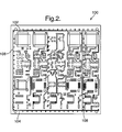
- Fig. 2 depicts a top view of an exemplary substrate 100 including a first graduated horizontal line 102 and a second graduated horizontal line 104.
- the substrate 100 also includes a first graduated vertical line 106 and a second graduated vertical line 108.
- the horizontal lines 102 and 104 include spaced marks oriented in a vertical direction.
- the vertical lines 106 and 108 include horizontal-spaced marks.
- the horizontal and vertical marks may be spaced, for example, every one-eighth of an inch.
- the marks are used to determine the amount of substrate 100 shrinkage that has occurred after curing, e.g., after firing.
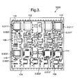
- the re-location, based upon the substrate 100 shrinkage after firing, of a number of electronic components 110, 112, 114 and 116 on the substrate 100, of electronic assembly 100A is further depicted.
- the location of the solder paste for the component 110 is adjusted upward by eleven-thousandths of an inch and to the left by two-thousandths of an inch.
- the solder paste for the electronic component 112 is adjusted upward by eleven-thousandths of an inch and to the left by seventeen-thousandths of an inch.
- the solder paste for the electronic component 116 is adjusted upward by three-thousandths of an inch and to the left by two-thousandths of an inch.
- solder paste for the component 114 is adjusted upward by three-thousandths of an inch and to the left by thirteen-thousandths of an inch.
- Fig. 4 depicts an exemplary process 400 for a green substrate, e.g., a green low-temperature co-fired ceramic (LTCC) substrate.
- a green substrate e.g., a green low-temperature co-fired ceramic (LTCC) substrate.
- LTCC green low-temperature co-fired ceramic
- step 402 a plurality of one or more horizontal and vertical lines are placed in a top metal level of a green LTCC substrate.
- the LTCC substrate is fired.
- shrinkage measurements are taken to determine both global and local shrinkage. As noted above, a random sample of several substrates may be used to determine appropriate corrections.
- the artwork associated with the solder and/or flux stencil is corrected.
- the shrinkage compensated solder/flux stencil is produced for use in manufacture of the electronic assembly.
Landscapes
- Engineering & Computer Science (AREA)
- Microelectronics & Electronic Packaging (AREA)
- Electric Connection Of Electric Components To Printed Circuits (AREA)
- Structure Of Printed Boards (AREA)
- Multi-Conductor Connections (AREA)
Abstract
Description
- The present invention is generally directed to an electronic assembly and, more specifically, to a technique for compensating for substrate shrinkage during manufacture of an electronic assembly.
- Substrates of electronic assemblies are made of a variety of materials that are subject to shrinkage, when the substrates are cured. For example, the green tape for low-temperature co-fired ceramic (LTCC) substrates shrinks upon firing, which can result in difficulty in precisely locating solder pads for proper printing of flux and solder on the solder pads. Furthermore, solder/flux stencil design has not taken into account the variation in substrate shrinkage across the substrate and within specific regions of the substrate. In general, the amount of substrate shrinkage has been predicted from an expected shrinkage, based on materials used and the process steps implemented.
- In a typical case, substrate shrinkage can result in a plus or minus 0.4 percent uncertainty, e.g., about twenty mils over a five inch substrate, in the location of a particular solder pad. On circuits built on larger substrate panels, e.g., six inch by six inch panels, the shrinkage of the substrate material may result in unacceptable product builds. This is especially true where large panels are structured in an array-type format. In general, current substrate shrinkage compensation techniques utilize post-firing substrate measurements to correct an initial 1:1 artwork used to create a solder stencil. In this manner, the overall solder stencil artwork is corrected for the substrate shrinkage globally.
However, the solder stencil artwork is not corrected for non-uniform shrinkage, which may be caused by a metallization difference, across the substrate. - With reference to Fig. 1, a relevant portion of a
prior art substrate 10 is depicted that includes a plurality ofconductive traces 12 that are coupled tosolder pads solder 14A has been misprinted such that it is only partially located on thepads 14. Similarly,solder 16A has been misprinted such that it only partially touches thesolder pad 16. While such misregistered solder prints may provide a functional electronic assembly, depending upon the type of electronic components utilized in the assembly, a misaligned solder stencil may cause an electronic assembly that utilizes fine lead pitch electronic components, e.g., components having a pitch of about twenty mils or less, to be defective. - What is needed is a technique for compensating for substrate shrinkage during manufacture of an electronic assembly that prevents improper solder placement.
- The present invention is generally directed to a technique for compensating for substrate shrinkage during manufacture of an electronic assembly. According to the technique, a horizontal line, having a plurality of vertical graduations, is provided across a horizontal portion of a substrate. A vertical line, having a plurality of horizontal graduations, is also provided across a vertical portion of the substrate. The substrate is then cured and an amount of shrinkage of the substrate is determined, based upon a location change in the graduations of the horizontal and vertical lines. Thus, solder can be provided on solder pads of the substrate responsive to the amount of substrate shrinkage. As such, electronic components can be properly mounted to the solder pads of the substrate.
- According to one aspect of the present invention, the horizontal and vertical lines may be formed in a top level metal layer of the substrate. According to a different aspect of the present invention, the horizontal and vertical lines provide an indication of a global shrinkage of the substrate, a local shrinkage of the substrate and a shrinkage of the substrate at each of the electronic components. The horizontal line may include two graduated parallel horizontal lines and the vertical line may include two graduated parallel vertical lines, with the parallel horizontal lines and the parallel vertical lines framing the substrate.
- According to one embodiment of the present invention, the substrate is a low-temperature co-fired ceramic (LTCC) substrate. The substrate may have various dimensions. For example, the substrate may have a dimension of about six inches by six inches or greater. According to another aspect of the present invention, flux is also provided on the solder pads of the substrate responsive to the amount of substrate shrinkage. prior to providing solder on the solder pads.
- These and other features, advantages and objects of the present invention will be further understood and appreciated by those skilled in the art by reference to the following specification, claims and appended drawings.
- The present invention will now be described, by way of example, with reference to the accompanying drawings, in which:
- Fig. 1 is a top view of a relevant portion of an exemplary prior art substrate with mis-registered solder;
- Fig. 2 is a top view of a substrate of an electronic assembly that includes a horizontal line, having a plurality of vertical graduations, and a vertical line, having a plurality of horizontal graduations, both of which are utilized to compensate for substrate shrinkage, according to the present invention;
- Fig. 3 is a top view of a relevant portion of the substrate of Fig. 2, depicting mounting of various components onto the substrate, based upon local adjustments for component location, due to local shrinkage of the substrate; and
- Fig. 4 is a flow chart of an exemplary process for implementing one embodiment of the present invention.
- According to one embodiment of the present invention, a top metal layer of a substrate is configured to include a frame made up of graduated lines. The graduated lines (markers) are used to obtain X and Y coordinate measurements to assist in determining the overall substrate shrinkage, the amount of substrate shrinkage at different locations across the substrate and the amount of substrate shrinkage at various component locations. According to the present invention, coordinate data may then be gathered, on a random sample basis, from multiple substrates, e.g., low-temperature co-fired ceramic (LTCC) substrates, to form a basis for solder and flux location adjustment.
- Thus, through the use of the X and Y coordinate data obtained from the markers, the solder or flux stencil can be modified, to improve the fit to the component pads on a component-by-component basis. The modified stencil is then corrected for both the overall shrinkage of the substrate and for the local substrate shrinkage variations, caused by, for example, internal metal loading within the substrate. Thus, implementing the present invention allows for corrected solder print and placement of fine pitch electronic components. The corrected artwork for the flux and solder placement is then developed, based upon the obtained shrinkage measurements. Assuming the design of the substrate has been frozen and the processing of the substrate is controlled, the gridlines may be eliminated and other control features may be chosen.
- Fig. 2 depicts a top view of an
exemplary substrate 100 including a first graduatedhorizontal line 102 and a second graduatedhorizontal line 104. Thesubstrate 100 also includes a first graduatedvertical line 106 and a second graduatedvertical line 108. As is shown, thehorizontal lines vertical lines substrate 100 shrinkage that has occurred after curing, e.g., after firing. - With reference to Fig. 3, the re-location, based upon the
substrate 100 shrinkage after firing, of a number ofelectronic components substrate 100, ofelectronic assembly 100A, is further depicted. As is shown in Fig. 3, the location of the solder paste for thecomponent 110 is adjusted upward by eleven-thousandths of an inch and to the left by two-thousandths of an inch. Similarly, the solder paste for theelectronic component 112 is adjusted upward by eleven-thousandths of an inch and to the left by seventeen-thousandths of an inch. Likewise, the solder paste for theelectronic component 116 is adjusted upward by three-thousandths of an inch and to the left by two-thousandths of an inch. Finally, the solder paste for thecomponent 114 is adjusted upward by three-thousandths of an inch and to the left by thirteen-thousandths of an inch. Thus, implementing the substrate shrinkage compensation technique of the present invention allows the components 110-116 to be independently adjusted, as needed, to compensate for local shrinkage of thesubstrate 100 at different locations. - Fig. 4 depicts an
exemplary process 400 for a green substrate, e.g., a green low-temperature co-fired ceramic (LTCC) substrate. Instep 402, a plurality of one or more horizontal and vertical lines are placed in a top metal level of a green LTCC substrate. Next, instep 404, the LTCC substrate is fired. Then, instep 406, shrinkage measurements are taken to determine both global and local shrinkage. As noted above, a random sample of several substrates may be used to determine appropriate corrections. Next, instep 408, the artwork associated with the solder and/or flux stencil is corrected. Finally, instep 410, the shrinkage compensated solder/flux stencil is produced for use in manufacture of the electronic assembly. - Accordingly, a technique has been disclosed herein that allows for local shrinkage compensation of a substrate. This is advantageous as it reduces scrap, as well as rework, of an electronic assembly.
- The above description is considered that of the preferred embodiments only. Modifications of the invention will occur to those skilled in the art and to those who make or use the invention. Therefore, it is understood that the embodiments shown in the drawings and described above are merely for illustrative purposes and not intended to limit the scope of the invention, which is defined by the following claims as interpreted according to the principles of patent law, including the doctrine of equivalents.
Claims (19)
- A method (400) for compensating for substrate shrinkage during manufacture of an electronic assembly, comprising the steps of:providing a horizontal line having a plurality of vertical graduations across a horizontal portion of a substrate (402);providing a vertical line having a plurality of horizontal graduations across a vertical portion of the substrate (402);curing the substrate (404);determining an amount of shrinkage of the substrate based upon a location change in the graduations of the horizontal and vertical lines (406);providing solder on solder pads of the substrate responsive to the amount of substrate shrinkage (408,410); andmounting electronic components to the solder pads.
- The method (400) of claim 1, wherein the horizontal and vertical lines are formed in a top level metal layer of the substrate.
- The method (400) of claim 1, wherein the horizontal and vertical lines provide an indication of a global shrinkage of the substrate, a local shrinkage of the substrate and a shrinkage of the substrate where each of the electronic components are placed.
- The method (400) of claim 1, wherein the horizontal line includes two graduated parallel horizontal lines and the vertical line includes two graduated parallel vertical lines, and wherein the horizontal and vertical lines frame the substrate.
- The method (400) of claim 1, wherein the substrate is a low-temperature co-fired ceramic (LTCC) substrate.
- The method (400) of claim 1, wherein the substrate has dimensions of about six inches by six inches or greater.
- The method (400) of claim 1, further comprising the step of:providing flux on the solder pads of the substrate responsive to the amount of substrate shrinkage prior to providing solder on the solder pads.
- A method (400) for compensating for substrate shrinkage during manufacture of an electronic assembly, comprising the steps of:providing a horizontal line having a plurality of vertical graduations across a horizontal portion of a substrate (402);providing a vertical line having a plurality of horizontal graduations across a vertical portion of the substrate (402);curing the substrate (404);determining an amount of shrinkage of the substrate based upon a location change in the graduations of the horizontal and vertical lines (406); andproviding flux on solder pads of the substrate responsive to the determined amount of shrinkage of the substrate (408, 410), wherein the substrate is a low-temperature co-fired ceramic (LTCC) substrate, and wherein the horizontal and vertical lines are formed in a metal layer of the substrate.
- The method (400) of claim 8, further comprising the step of:providing solder on the solder pads of the substrate responsive to the amount of substrate shrinkage prior to providing solder on the solder pads (408, 410).
- The method (400) of claim 9, further comprising the step of:mounting electronic components to the solder pads.
- The method (400) of claim 10, wherein the horizontal and vertical lines provide an indication of a global shrinkage of the substrate, a local shrinkage of the substrate and a shrinkage of the substrate where each of the electronic components are placed.
- The method (400) of claim 8, wherein the horizontal line includes two graduated parallel horizontal lines and the vertical line includes two graduated parallel vertical lines, and wherein the horizontal and vertical lines frame the substrate.
- The method (400) of claim 8, wherein the substrate has dimensions of about six inches by six inches or greater.
- An electronic assembly (100A) with substrate shrinkage compensation, comprising:a substrate (100) having a horizontal line (102,104) having a plurality of vertical graduations across a horizontal portion of the substrate (100) and vertical line (106,108) having a plurality of horizontal graduations across a vertical portion of the substrate (100), wherein the substrate (100) includes a plurality of solder pads formed on at least one surface of the substrate (100); anda plurality of electronic components (110,112,114,116) coupled to one or more of the solder pads, wherein an amount of substrate shrinkage is determined based upon a location change in the graduations of the horizontal and vertical lines (102,104,106,108) and a solder that electrically connects the electronic components (110,112,114,116) to the solder pads is deposited on the solder pads responsive to the amount of substrate shrinkage.
- The assembly (100A) of claim 14, wherein the substrate (100) is a low-temperature co-fired ceramic (LTCC) substrate.
- The assembly (100A) of claim 14, wherein the horizontal and vertical lines (102,104,106,108) are formed in a metal layer of the substrate (100).
- The assembly (100A) of claim 14, wherein the horizontal and vertical lines (102,104,106,108) provide an indication of a global shrinkage of the substrate (100), a local shrinkage of the substrate (100) and a shrinkage of the substrate (100) where each of the electronic components (110,112,114,116) are placed.
- The assembly (100A) of claim 14, wherein the horizontal line (102,104) includes two graduated parallel horizontal lines and the vertical line (106,108) includes two graduated parallel vertical lines, and wherein the horizontal and vertical lines (102,104,106,108) form a frame on the substrate (100).
- The assembly (100A) of claim 14, wherein the substrate (100) has dimensions of about six inches by six inches or greater.
Applications Claiming Priority (1)
| Application Number | Priority Date | Filing Date | Title |
|---|---|---|---|
| US11/105,927 US7439083B2 (en) | 2005-04-14 | 2005-04-14 | Technique for compensating for substrate shrinkage during manufacture of an electronic assembly |
Publications (2)
| Publication Number | Publication Date |
|---|---|
| EP1718138A2 true EP1718138A2 (en) | 2006-11-02 |
| EP1718138A3 EP1718138A3 (en) | 2007-08-08 |
Family
ID=36942266
Family Applications (1)
| Application Number | Title | Priority Date | Filing Date |
|---|---|---|---|
| EP06075721A Withdrawn EP1718138A3 (en) | 2005-04-14 | 2006-03-29 | Technique for compensating for substrate shrinkage during manufacture of an electronic assembly |
Country Status (2)
| Country | Link |
|---|---|
| US (1) | US7439083B2 (en) |
| EP (1) | EP1718138A3 (en) |
Families Citing this family (1)
| Publication number | Priority date | Publication date | Assignee | Title |
|---|---|---|---|---|
| TWI724705B (en) | 2019-12-20 | 2021-04-11 | 財團法人工業技術研究院 | Method for compensating design image of workpiece and system for processing design image of workpiece |
Family Cites Families (7)
| Publication number | Priority date | Publication date | Assignee | Title |
|---|---|---|---|---|
| DE3305325C1 (en) | 1983-02-16 | 1984-05-24 | Siemens AG, 1000 Berlin und 8000 München | Template and method for subsequent changes to connections on assembled circuit boards with a narrow solder eye grid |
| US5162240A (en) | 1989-06-16 | 1992-11-10 | Hitachi, Ltd. | Method and apparatus of fabricating electric circuit pattern on thick and thin film hybrid multilayer wiring substrate |
| US20010049589A1 (en) * | 1993-01-21 | 2001-12-06 | Nikon Corporation | Alignment method and apparatus therefor |
| US5385289A (en) | 1994-02-08 | 1995-01-31 | Digital Equipment Corporation | Embedded features for registration measurement in electronics manufacturing |
| JP4053723B2 (en) * | 2000-09-27 | 2008-02-27 | 株式会社東芝 | Method for manufacturing exposure mask |
| US6581202B1 (en) | 2000-11-10 | 2003-06-17 | Viasystems Group, Inc. | System and method for monitoring and improving dimensional stability and registration accuracy of multi-layer PCB manufacture |
| JP2003007608A (en) * | 2001-06-27 | 2003-01-10 | Canon Inc | Alignment method, exposure apparatus and device manufacturing method |
-
2005
- 2005-04-14 US US11/105,927 patent/US7439083B2/en not_active Expired - Fee Related
-
2006
- 2006-03-29 EP EP06075721A patent/EP1718138A3/en not_active Withdrawn
Also Published As
| Publication number | Publication date |
|---|---|
| US7439083B2 (en) | 2008-10-21 |
| EP1718138A3 (en) | 2007-08-08 |
| US20060234424A1 (en) | 2006-10-19 |
Similar Documents
| Publication | Publication Date | Title |
|---|---|---|
| US6169253B1 (en) | Solder resist window configurations for solder paste overprinting | |
| KR101175871B1 (en) | Method for revision of printing error in pcb | |
| CN100515158C (en) | Printed wiring board, manufacturing method therefor, and mounting method therefor | |
| US20060086773A1 (en) | Technique for optical inspection system verification | |
| US7439083B2 (en) | Technique for compensating for substrate shrinkage during manufacture of an electronic assembly | |
| JP3128891B2 (en) | Component mounting method and component mounting device | |
| US20050243536A1 (en) | Printed circuit board, parts mounting method and mounting position verifying method | |
| US5385289A (en) | Embedded features for registration measurement in electronics manufacturing | |
| JP2003163449A (en) | How to mount chip components | |
| JP2553786B2 (en) | Circuit board recognition mark placement method | |
| US20060087031A1 (en) | Assembly and method | |
| JPH0738519B2 (en) | Electronic component mounting method | |
| JP2007189101A (en) | Electronic component mounting method | |
| JP3692678B2 (en) | Screen printing method | |
| JPH02122590A (en) | Parts positioning device | |
| JPH11307890A (en) | Printed wiring board | |
| JPH0227831B2 (en) | PURINTOHAISENBAN | |
| CN111050481B (en) | PCB board tombstone effect printing method | |
| JPH05145215A (en) | Method of forming positioning mark for printed wiring board | |
| JPH07335411A (en) | Chip resistor network | |
| JP2695060B2 (en) | Thick film wiring board having a plurality of identical circuit patterns | |
| Klein Wassink | Footprints of Fine Pitch SMDs | |
| JP2743175B2 (en) | Solder resist plate for printed circuit board and method for manufacturing printed circuit board | |
| JPH06326446A (en) | Board and manufacture thereof | |
| JPH1117292A (en) | Printed circuit board and component mounter for mounting components on this board |
Legal Events
| Date | Code | Title | Description |
|---|---|---|---|
| PUAI | Public reference made under article 153(3) epc to a published international application that has entered the european phase |
Free format text: ORIGINAL CODE: 0009012 |
|
| AK | Designated contracting states |
Kind code of ref document: A2 Designated state(s): AT BE BG CH CY CZ DE DK EE ES FI FR GB GR HU IE IS IT LI LT LU LV MC NL PL PT RO SE SI SK TR |
|
| AX | Request for extension of the european patent |
Extension state: AL BA HR MK YU |
|
| PUAL | Search report despatched |
Free format text: ORIGINAL CODE: 0009013 |
|
| AK | Designated contracting states |
Kind code of ref document: A3 Designated state(s): AT BE BG CH CY CZ DE DK EE ES FI FR GB GR HU IE IS IT LI LT LU LV MC NL PL PT RO SE SI SK TR |
|
| AX | Request for extension of the european patent |
Extension state: AL BA HR MK YU |
|
| 17P | Request for examination filed |
Effective date: 20080208 |
|
| AKX | Designation fees paid |
Designated state(s): AT BE BG CH CY CZ DE DK EE ES FI FR GB GR HU IE IS IT LI LT LU LV MC NL PL PT RO SE SI SK TR |
|
| 17Q | First examination report despatched |
Effective date: 20080320 |
|
| STAA | Information on the status of an ep patent application or granted ep patent |
Free format text: STATUS: THE APPLICATION IS DEEMED TO BE WITHDRAWN |
|
| 18D | Application deemed to be withdrawn |
Effective date: 20101001 |