EP1717849A1 - Process for manufacturing a MOS device with intercell ion implant - Google Patents
Process for manufacturing a MOS device with intercell ion implant Download PDFInfo
- Publication number
- EP1717849A1 EP1717849A1 EP05425260A EP05425260A EP1717849A1 EP 1717849 A1 EP1717849 A1 EP 1717849A1 EP 05425260 A EP05425260 A EP 05425260A EP 05425260 A EP05425260 A EP 05425260A EP 1717849 A1 EP1717849 A1 EP 1717849A1
- Authority
- EP
- European Patent Office
- Prior art keywords
- enrichment
- window
- region
- gate structure
- layer
- Prior art date
- Legal status (The legal status is an assumption and is not a legal conclusion. Google has not performed a legal analysis and makes no representation as to the accuracy of the status listed.)
- Withdrawn
Links
- 238000000034 method Methods 0.000 title claims abstract description 29
- 230000008569 process Effects 0.000 title claims abstract description 24
- 238000004519 manufacturing process Methods 0.000 title claims abstract description 17
- 239000007943 implant Substances 0.000 title description 10
- 239000004065 semiconductor Substances 0.000 claims abstract description 32
- 239000002019 doping agent Substances 0.000 claims abstract description 6
- 210000000746 body region Anatomy 0.000 claims abstract 10
- 239000003989 dielectric material Substances 0.000 claims description 17
- 239000000463 material Substances 0.000 claims description 14
- 238000005530 etching Methods 0.000 claims description 12
- 230000004888 barrier function Effects 0.000 claims description 7
- 238000000151 deposition Methods 0.000 claims description 7
- 238000009413 insulation Methods 0.000 claims description 7
- 229910021420 polycrystalline silicon Inorganic materials 0.000 claims description 4
- 229920005591 polysilicon Polymers 0.000 claims description 4
- 125000006850 spacer group Chemical group 0.000 claims description 4
- 239000004020 conductor Substances 0.000 claims 4
- 238000005468 ion implantation Methods 0.000 description 12
- 239000000758 substrate Substances 0.000 description 10
- 150000002500 ions Chemical class 0.000 description 7
- 230000009467 reduction Effects 0.000 description 7
- 230000015572 biosynthetic process Effects 0.000 description 6
- 229910052581 Si3N4 Inorganic materials 0.000 description 5
- 239000000945 filler Substances 0.000 description 5
- HQVNEWCFYHHQES-UHFFFAOYSA-N silicon nitride Chemical compound N12[Si]34N5[Si]62N3[Si]51N64 HQVNEWCFYHHQES-UHFFFAOYSA-N 0.000 description 5
- 230000008021 deposition Effects 0.000 description 4
- 239000011810 insulating material Substances 0.000 description 4
- 238000000926 separation method Methods 0.000 description 4
- BOTDANWDWHJENH-UHFFFAOYSA-N Tetraethyl orthosilicate Chemical compound CCO[Si](OCC)(OCC)OCC BOTDANWDWHJENH-UHFFFAOYSA-N 0.000 description 3
- 238000005229 chemical vapour deposition Methods 0.000 description 3
- 238000009792 diffusion process Methods 0.000 description 3
- 230000005684 electric field Effects 0.000 description 3
- 230000000873 masking effect Effects 0.000 description 3
- 239000007769 metal material Substances 0.000 description 3
- 238000001465 metallisation Methods 0.000 description 3
- 238000004806 packaging method and process Methods 0.000 description 3
- 239000005360 phosphosilicate glass Substances 0.000 description 3
- XUIMIQQOPSSXEZ-UHFFFAOYSA-N Silicon Chemical compound [Si] XUIMIQQOPSSXEZ-UHFFFAOYSA-N 0.000 description 2
- 230000007423 decrease Effects 0.000 description 2
- 238000000280 densification Methods 0.000 description 2
- 238000009826 distribution Methods 0.000 description 2
- 238000005516 engineering process Methods 0.000 description 2
- 230000004048 modification Effects 0.000 description 2
- 238000012986 modification Methods 0.000 description 2
- 229910052710 silicon Inorganic materials 0.000 description 2
- 239000010703 silicon Substances 0.000 description 2
- 238000001039 wet etching Methods 0.000 description 2
- 230000004075 alteration Effects 0.000 description 1
- 239000000969 carrier Substances 0.000 description 1
- 230000015556 catabolic process Effects 0.000 description 1
- 239000002800 charge carrier Substances 0.000 description 1
- 238000006731 degradation reaction Methods 0.000 description 1
- 238000001312 dry etching Methods 0.000 description 1
- 230000009977 dual effect Effects 0.000 description 1
- 238000007687 exposure technique Methods 0.000 description 1
- 239000011521 glass Substances 0.000 description 1
- 229910044991 metal oxide Inorganic materials 0.000 description 1
- 150000004706 metal oxides Chemical class 0.000 description 1
- 150000004767 nitrides Chemical class 0.000 description 1
- 230000003647 oxidation Effects 0.000 description 1
- 238000007254 oxidation reaction Methods 0.000 description 1
- 238000000206 photolithography Methods 0.000 description 1
- 229920002120 photoresistant polymer Polymers 0.000 description 1
- 238000007747 plating Methods 0.000 description 1
- 238000002360 preparation method Methods 0.000 description 1
- 230000035945 sensitivity Effects 0.000 description 1
- 229910021332 silicide Inorganic materials 0.000 description 1
- FVBUAEGBCNSCDD-UHFFFAOYSA-N silicide(4-) Chemical compound [Si-4] FVBUAEGBCNSCDD-UHFFFAOYSA-N 0.000 description 1
Images



Classifications
-
- H—ELECTRICITY
- H10—SEMICONDUCTOR DEVICES; ELECTRIC SOLID-STATE DEVICES NOT OTHERWISE PROVIDED FOR
- H10D—INORGANIC ELECTRIC SEMICONDUCTOR DEVICES
- H10D30/00—Field-effect transistors [FET]
- H10D30/60—Insulated-gate field-effect transistors [IGFET]
- H10D30/64—Double-diffused metal-oxide semiconductor [DMOS] FETs
- H10D30/66—Vertical DMOS [VDMOS] FETs
-
- H—ELECTRICITY
- H10—SEMICONDUCTOR DEVICES; ELECTRIC SOLID-STATE DEVICES NOT OTHERWISE PROVIDED FOR
- H10D—INORGANIC ELECTRIC SEMICONDUCTOR DEVICES
- H10D30/00—Field-effect transistors [FET]
- H10D30/01—Manufacture or treatment
- H10D30/021—Manufacture or treatment of FETs having insulated gates [IGFET]
- H10D30/028—Manufacture or treatment of FETs having insulated gates [IGFET] of double-diffused metal oxide semiconductor [DMOS] FETs
- H10D30/0291—Manufacture or treatment of FETs having insulated gates [IGFET] of double-diffused metal oxide semiconductor [DMOS] FETs of vertical DMOS [VDMOS] FETs
- H10D30/0293—Manufacture or treatment of FETs having insulated gates [IGFET] of double-diffused metal oxide semiconductor [DMOS] FETs of vertical DMOS [VDMOS] FETs using formation of insulating sidewall spacers
-
- H—ELECTRICITY
- H10—SEMICONDUCTOR DEVICES; ELECTRIC SOLID-STATE DEVICES NOT OTHERWISE PROVIDED FOR
- H10D—INORGANIC ELECTRIC SEMICONDUCTOR DEVICES
- H10D30/00—Field-effect transistors [FET]
- H10D30/60—Insulated-gate field-effect transistors [IGFET]
- H10D30/64—Double-diffused metal-oxide semiconductor [DMOS] FETs
- H10D30/66—Vertical DMOS [VDMOS] FETs
- H10D30/662—Vertical DMOS [VDMOS] FETs having a drift region having a doping concentration that is higher between adjacent body regions relative to other parts of the drift region
-
- H—ELECTRICITY
- H10—SEMICONDUCTOR DEVICES; ELECTRIC SOLID-STATE DEVICES NOT OTHERWISE PROVIDED FOR
- H10D—INORGANIC ELECTRIC SEMICONDUCTOR DEVICES
- H10D62/00—Semiconductor bodies, or regions thereof, of devices having potential barriers
- H10D62/10—Shapes, relative sizes or dispositions of the regions of the semiconductor bodies; Shapes of the semiconductor bodies
- H10D62/13—Semiconductor regions connected to electrodes carrying current to be rectified, amplified or switched, e.g. source or drain regions
- H10D62/149—Source or drain regions of field-effect devices
- H10D62/151—Source or drain regions of field-effect devices of IGFETs
- H10D62/156—Drain regions of DMOS transistors
- H10D62/157—Impurity concentrations or distributions
-
- H—ELECTRICITY
- H10—SEMICONDUCTOR DEVICES; ELECTRIC SOLID-STATE DEVICES NOT OTHERWISE PROVIDED FOR
- H10D—INORGANIC ELECTRIC SEMICONDUCTOR DEVICES
- H10D64/00—Electrodes of devices having potential barriers
- H10D64/20—Electrodes characterised by their shapes, relative sizes or dispositions
- H10D64/27—Electrodes not carrying the current to be rectified, amplified, oscillated or switched, e.g. gates
- H10D64/311—Gate electrodes for field-effect devices
- H10D64/411—Gate electrodes for field-effect devices for FETs
- H10D64/511—Gate electrodes for field-effect devices for FETs for IGFETs
- H10D64/517—Gate electrodes for field-effect devices for FETs for IGFETs characterised by the conducting layers
- H10D64/518—Gate electrodes for field-effect devices for FETs for IGFETs characterised by the conducting layers characterised by their lengths or sectional shapes
-
- H—ELECTRICITY
- H10—SEMICONDUCTOR DEVICES; ELECTRIC SOLID-STATE DEVICES NOT OTHERWISE PROVIDED FOR
- H10D—INORGANIC ELECTRIC SEMICONDUCTOR DEVICES
- H10D64/00—Electrodes of devices having potential barriers
- H10D64/20—Electrodes characterised by their shapes, relative sizes or dispositions
- H10D64/27—Electrodes not carrying the current to be rectified, amplified, oscillated or switched, e.g. gates
- H10D64/311—Gate electrodes for field-effect devices
- H10D64/411—Gate electrodes for field-effect devices for FETs
- H10D64/511—Gate electrodes for field-effect devices for FETs for IGFETs
- H10D64/517—Gate electrodes for field-effect devices for FETs for IGFETs characterised by the conducting layers
- H10D64/519—Gate electrodes for field-effect devices for FETs for IGFETs characterised by the conducting layers characterised by their top-view geometrical layouts
Definitions
- the present invention relates to a process for manufacturing a MOS device with intercell ion implant, in particular a VDMOS (Vertical Double-Diffused Metal Oxide Semiconductor) power device, to which the following description will make explicit reference without this implying any loss of generality.
- VDMOS Very Double-Diffused Metal Oxide Semiconductor
- a VDMOS device 1 comprises a substrate 2 of a heavily doped semiconductor material (for example, of an N + type), and an epitaxial layer 3, which is also made of semiconductor material with the same type of conductivity as the substrate 2, and overlies the substrate 2.
- cells 5 of the VDMOS device 1 are formed, each comprising a body well 6 having a conductivity opposite to that of the epitaxial layer 3 (in the given example, of a P type), and a source region 8, within the body well 6, having the same type of conductivity as the substrate 2 (in the example, of an N + type).
- the portion of the epitaxial layer 3 set between adjacent body wells 6 is commonly referred to as “intercell region” or “drift region”.
- the VDMOS device 1 further comprises: an insulated gate structure 9, made by a first region of dielectric material 10 formed above the drift region and partially overlying the body wells 6 and the source regions 8; a gate electrode 11, formed over the first region of dielectric material 10; and a second region of dielectric material 12, overlying the gate electrode 11.
- a body/source metallization 14 is formed above the body wells 6 for contacting the body wells 6 and the source regions 8, and a drain metallization 15 contacts the substrate 2 from the back.
- the substrate 2 has the function of drain for the VDMOS device 1, and the epitaxial layer 3 represents a surface extension thereof.
- the channel of each cell 5 is constituted by the portion of the corresponding body well 6 arranged directly underneath the insulated gate structure 9, and is delimited by the junction between the source region 8 and the body well 6 on the one hand, and by the junction between the body well 6 and the drift region, on the other hand.
- the gate electrode 11 is capacitively coupled to the channel for modulating the type of conductivity thereof. In particular, via the application of an appropriate voltage to the gate electrode 11, it is possible to cause the inversion of the channel and thus create a conductive path for the majority charge carriers between the source region 8 and the substrate 2, through the channel, and the drift region.
- the resulting current flow (designated by I in Figure 1) is affected by the resistance of the channel and drift regions.
- VDMOS devices As is known, the reduction in the planar and vertical dimensions of VDMOS devices, necessary for the purpose of increasing the packaging density in low-consumption power technologies, leads to a series of problems that limit the performance of VDMOS devices.
- said reduction leads to an increase in the sensitivity of VDMOS devices to the surface electrical field in the proximity of the active drain and/or body junctions, and an increase in the contribution of the surface portion of the drift region (commonly known as J-FET contribution) to the ON-resistance R dson of the VDMOS devices.
- the reduction in the lateral separation between contiguous cells 5 enables the increase in the conductive channel perimeter per unit of active area, on the other hand it causes a greater narrowing in the path of the current I, and an increase in the ON-resistance R dson .
- This increase is of particular importance in the case of VDMOS devices of low voltage (less than 100 V), and high packaging density.
- the enrichment ion implantation is provided with photolithographic techniques prior to defining the insulated gate structure 9.
- An appropriate masking is defined, which will delineate the area of the enrichment implant in such a way as not to involve the channel of the VDMOS device, and an ion implantation of an appropriate dopant species is subsequently performed through said masking.
- a solution of this type has, however, some drawbacks.
- the alignment between the enrichment ion implant and the channel becomes increasingly critical.
- the possible misalignments of the implant with respect to the body and source active junctions can lead, for scaled planar geometries, to a non-uniformity of the threshold voltage of the VDMOS devices.
- the dielectric of the first region of dielectric material 10 when grown above the enrichment region, shows an increase in the intrinsic defectiveness, and so a greater criticality in terms of reliability.
- the enrichment ion implantation is provided in an initial step of the process for manufacturing the VDMOS device, prior to formation of the insulated gate structure 9.
- a uniform surface ion implantation (of a blanket type) is made directly in the epitaxial layer 3, without the use of purposely provided masks.
- said solution is not free from problems, amongst which the degradation in the quality of the dielectric of the first region of dielectric material 10, when this is grown above the enrichment region.
- the aim of the present invention is consequently to provide a process for manufacturing a MOS device with intercell ion implant which will enable the problems and disadvantages referred to above to be overcome.
- a process for manufacturing a MOS device and a corresponding MOS device are provided, as defined in Claim 1 and Claim 11, respectively.
- the process for manufacturing a VDMOS power device first envisages provision of a wafer 21 of semiconductor material, preferably silicon, comprising a substrate 22 (illustrated only in Figure 2), heavily doped and having a first type of conductivity (for example, of an N + type). Then, a semiconductor layer 23, having the same type of conductivity (in the example, of an N type) as the substrate 22, is formed, for example via an epitaxial growth, above the substrate 22. In a per se known manner which is not described in detail, edge termination structures (not shown) of the VDMOS device are formed, and consequently an active area is defined wherein elementary functional units of the VDMOS device will be provided.
- the gate dielectric layer 24 can be formed via a thermal oxidation, or else via deposition of an oxynitride layer or of a multilayer constituted by successive layers of oxide, nitride, and oxide laid on top of one another.
- a gate-electrode layer 25, of polysilicon (intrinsic, or possibly doped), is deposited on the gate dielectric layer 24. Alternatively, a double layer formed by polysilicon and metallic silicide can be deposited.
- a layer of insulating material 26 is then deposited, via CVD (Chemical Vapour Deposition).
- the layer of insulating material 26 can for example be of TEOS (Tetra-Ethyl-OrthoSilicate), USG (Undoped Silicon Glass), or PSG (Phosphosilicate Glass).
- an insulated gate structure 27 is defined using a photolithographic technique on the semiconductor layer 23.
- a one-directional etching of the layer of insulating material 26 is first performed with end-point on the gate-electrode layer 25, and then a one-directional etching of the gate-electrode layer 25 is performed for a pre-set time, or else with end-point on the gate dielectric layer 24.
- the resulting insulated gate structure 27 comprises a plurality of gate portions 28, which have a stripe-like shape and extend parallel to one another in a first direction x.
- the gate portions 28 are constituted by the superposition of portions of the gate dielectric layer 24, of the gate-electrode layer 25 (in the following said portions will be referred to as gate electrodes 25), and of the layer of insulating material 26, and are separated by body/source windows 29 in a second direction y, orthogonal to the first direction x.
- the body/source windows 29 have a minor dimension L 1 (in the following width L 1 ) in the second direction y.
- the insulated gate structure 27 further comprises connection elements (not shown) connecting the gate portions 28 in a comblike structure, of a type known for power devices.
- enrichment windows 30 are opened within the gate portions 28, enabling access to portions of the semiconductor layer 23 which are designed (as described in detail hereinafter) for the formation of intercell enrichment ion implants between adjacent elementary functional units of the VDMOS device.
- a plurality of enrichment windows 30 is opened, said windows being aligned to one another in the first direction x, in a central position with respect to the respective gate portion 28.
- the enrichment windows 30 have an approximately rectangular shape, with a major dimension 1 (in the following, length 1) in the first direction x, and a minor dimension L 2 (in the following, width L 2 ) in the second direction y.
- the width L 2 of the enrichment windows 30 is smaller than the width L 1 of the body/source windows 29; in particular, the ratio L 1 /L 2 is preferably greater than or equal to 2.
- the enrichment windows 30 are separated from one another by a separation gap s, in the first direction x.
- the ratio between the length 1 of the enrichment windows 30 and the separation gap s must be appropriately sized, taking into account the design and performance requirements of the VDMOS device, and in particular the switching speed, which depends upon the resistance of the insulated gate structure 27 and upon the distributed capacitance between the insulated gate structure 27 and the electrodes of the VDMOS device (source, body and drain).
- the interruption of the gate-electrode layer 25 affects both the resistance of the gate electrode and the distribution of the gate electric field in the proximity of the enrichment windows 30.
- the manufacturing process proceeds (see Figure 5) with the deposition of a thin silicon-nitride layer 34, having, for example, a thickness smaller than 50 nm, and a high degree of conformality.
- a layer of sacrificial material 35 is then deposited, constituted by polysilicon, either intrinsic or doped.
- the thickness of the layer of sacrificial material 35 is greater than the half-width of the enrichment windows 30 (i.e., greater than L 2 /2).
- each enrichment window 30 remains filled by a first barrier region 36, constituted by a remaining portion of the layer of sacrificial material 35.
- the maximum value of the width L 2 of the enrichment windows 30 must be such as to enable a filling by the first barrier region 36 to be obtained during the aforesaid etching step.
- the maximum value of the width L 2 is, for example, in the region of 1 ⁇ m.
- the minimum value of the width L 2 is instead determined by the technological limits of the photo-exposure technique used for the formation of the enrichment windows 30; for example, said minimum value is currently 0.25 ⁇ m.
- a one-directional (dry) etching of the silicon-nitride layer 34 is performed, for a pre-set time or else with end-point on the gate dielectric layer 24, and possibly a further one-directional etching of the gate dielectric layer 24.
- a first ion implantation is then performed, self-aligned with respect to the body/source windows 29, to obtain body wells 37 within the semiconductor layer 23.
- a second ion implantation is performed to obtain source regions 38 within the body wells 37.
- the first ion implantation has a type of conductivity opposite to that of the semiconductor layer 23 (in the example, of a P type), whilst the second ion implantation has a type of conductivity opposite to that of the first ion implantation (in the example, of an N + type). It should be noted, in particular, that the first and second ion implants are blocked within the enrichment windows 30 by the first barrier region 36.
- a photoresist layer is deposited and etched to form a mask 40, which entirely covers the body/source windows 29 and leaves, instead, exposed the enrichment windows 30.
- a wet etching of the first barrier regions 36 (possibly preceded by a slight etching of the first dielectric layer 26), and a dry etching of the underlying silicon-nitride layer 34, and optionally of the gate dielectric layer 24, are then performed.
- the mask 40 protects the body/source windows 29 from the aforesaid etching.
- the subsequent process step envisages a self-aligned ion implantation through the enrichment windows 30, following upon which enrichment regions 42 are formed having the same type of conductivity as the semiconductor layer 23 (in the example, of an N type).
- the enrichment regions 42 have the function of increasing the conductivity of the regions of the semiconductor layer 23 arranged between adjacent body wells 37 (drift regions) in order to reduce the ON-resistance R dson of the VDMOS device.
- the mask 40 protects the body/source windows 29 from the ion implantation.
- the mask 40 is then removed, and a diffusion of the enrichment region 42 is performed via an appropriate thermal process.
- a CVD deposition of a filler layer 43 is performed, the filler layer 43 being of a dielectric material with low conformality, the thickness of which depending upon the planar geometry of the VDMOS device; the dielectric material can be USG, PSG, TEOS, or any other dielectric or dielectric multilayer.
- a layer of metallic material 46 is formed on the wafer 21, having the function of contacting the source regions 38. Interruptions (not shown) of the source regions 38 are provided in the first direction x, in such a way that the layer of metallic material 46 contacts also the body wells 37.
- the insulation spacers 44 electrically insulate from one another the layer of metallic material 46 and the gate electrodes 25.
- the ratio between the thickness of the filler layer 43 and the width L 1 of the source/body windows 29 is to be sized (generally maximized) so as to obtain a robust and homogeneous lateral insulation of the gate electrodes 25. For example, the value of said ratio is comprised between 0.1 and 0.2.
- the manufacturing process of the VDMOS device terminates with the preparation and metallization of the back of the wafer 21 to provide a drain electrical contact.
- the enrichment windows 30 (and consequently the enrichment regions 42) have a different shape, in particular the shape of a rectangular annulus.
- Said embodiment is advantageous in VDMOS devices in which the distance between adjacent body wells 37 must be kept wide to reduce the J-FET contribution in the ON-resistance R dson .
- the enrichment regions 42 provided for reasons of symmetry in the proximity of the centre of the gate portions 28, would be too distant from the terminations of the conduction channel of the VDMOS device to cause a significant reduction in the ON-resistance R dson .
- the width of the windows is still compatible with the need for self-alignment of the enrichment regions 42, and at the same time the distance between the enrichment regions 42 and the channel terminations is sufficiently small as to guarantee a considerable reduction in the ON-resistance R dson .
- the definition of the enrichment windows 30, in this case brings about the formation of islands 48, which are physically separated from the gate electrode 25 and so cannot be directly biased. This leads to a reduction in the capacitance between the gate electrode 25 and the drain and in the charging time of the gate electrode 25. At the same time, there is no excessive alteration in the property of "field plating", which normally the gate electrode 25 exerts on the distribution of the drain electric field in the active region of the VDMOS device.
- a plurality of pairs of enrichment windows 30, aligned in the first direction x is defined within each gate portion 28.
- the enrichment windows 30 of each pair are rectangular, parallel to one another and to the first direction x and aligned in the second direction y; in addition, the enrichment windows 30 are provided in the proximity of the channel regions of the VDMOS device.
- the enrichment windows 30 are arranged symmetrically with respect to a central axis of the respective gate portion 28 extending in the first direction x.
- a further embodiment, illustrated in Figure 16 envisages the formation, within each gate portion 28, of a plurality of grids of enrichment windows 30 aligned in the first direction x.
- the enrichment windows 30 within each grid are rectangular and parallel to one another and to the first direction x, and are aligned in the second direction y and arranged symmetrically with respect to a central axis of the respective gate portion 28, extending in the first direction x.
- Said embodiment leads to an increase in the planar resistance of the gate electrode 25, but to a decrease in the ON-resistance R dson , due to the presence of a number of enrichment regions 42.
- the process for manufacturing the VDMOS device may be freed from the technological limits of the photolithographic processes, above all as regards highly scaled technologies.
- the enrichment regions enable a marked reduction in the ON-resistance of the VDMOS device, and at the same time characteristics such as planar resistance and gate capacitance are not significantly altered, without any consequent modification in the switching speed of the VDMOS device.
- the gate and source/body electrical contacts can be defined with photolithographic technique, i.e., without self-aligned formation of the insulation spacers in the body/source windows.
- the second layer of dielectric material does not necessarily have a low conformality, and must have a thickness greater than the half-width of the enrichment window.
- the corresponding process steps envisage deposition of the second layer of dielectric material, densification thereof, and then photolithography of the contacts, in a way in itself known and hence not described in detail herein.
- the described process can advantageously be applied for forming any kind of ion implant in the intercell region.
Landscapes
- Insulated Gate Type Field-Effect Transistor (AREA)
- Electrodes Of Semiconductors (AREA)
Abstract
Description
- The present invention relates to a process for manufacturing a MOS device with intercell ion implant, in particular a VDMOS (Vertical Double-Diffused Metal Oxide Semiconductor) power device, to which the following description will make explicit reference without this implying any loss of generality.
- As is known, and as is illustrated in Figure 1, a
VDMOS device 1 comprises asubstrate 2 of a heavily doped semiconductor material (for example, of an N+ type), and anepitaxial layer 3, which is also made of semiconductor material with the same type of conductivity as thesubstrate 2, and overlies thesubstrate 2. Within a surface portion of theepitaxial layer 3,cells 5 of theVDMOS device 1 are formed, each comprising a body well 6 having a conductivity opposite to that of the epitaxial layer 3 (in the given example, of a P type), and asource region 8, within the body well 6, having the same type of conductivity as the substrate 2 (in the example, of an N+ type). The portion of theepitaxial layer 3 set betweenadjacent body wells 6 is commonly referred to as "intercell region" or "drift region". TheVDMOS device 1 further comprises: an insulated gate structure 9, made by a first region ofdielectric material 10 formed above the drift region and partially overlying thebody wells 6 and thesource regions 8; agate electrode 11, formed over the first region ofdielectric material 10; and a second region ofdielectric material 12, overlying thegate electrode 11. A body/source metallization 14 is formed above thebody wells 6 for contacting thebody wells 6 and thesource regions 8, and adrain metallization 15 contacts thesubstrate 2 from the back. - The
substrate 2 has the function of drain for theVDMOS device 1, and theepitaxial layer 3 represents a surface extension thereof. The channel of eachcell 5 is constituted by the portion of the corresponding body well 6 arranged directly underneath the insulated gate structure 9, and is delimited by the junction between thesource region 8 and the body well 6 on the one hand, and by the junction between the body well 6 and the drift region, on the other hand. Thegate electrode 11 is capacitively coupled to the channel for modulating the type of conductivity thereof. In particular, via the application of an appropriate voltage to thegate electrode 11, it is possible to cause the inversion of the channel and thus create a conductive path for the majority charge carriers between thesource region 8 and thesubstrate 2, through the channel, and the drift region. The resulting current flow (designated by I in Figure 1) is affected by the resistance of the channel and drift regions. - As is known, the reduction in the planar and vertical dimensions of VDMOS devices, necessary for the purpose of increasing the packaging density in low-consumption power technologies, leads to a series of problems that limit the performance of VDMOS devices. In particular, said reduction leads to an increase in the sensitivity of VDMOS devices to the surface electrical field in the proximity of the active drain and/or body junctions, and an increase in the contribution of the surface portion of the drift region (commonly known as J-FET contribution) to the ON-resistance Rdson of the VDMOS devices. In this regard, if on the one hand the reduction in the lateral separation between
contiguous cells 5 enables the increase in the conductive channel perimeter per unit of active area, on the other hand it causes a greater narrowing in the path of the current I, and an increase in the ON-resistance Rdson. This increase is of particular importance in the case of VDMOS devices of low voltage (less than 100 V), and high packaging density. In order to limit this problem, without however renouncing high packaging densities, it has been proposed to increase the conductivity of the drift region and, in particular, to physically increase the number of majority carriers in the drift region, through a surface-enrichment ion implant betweencontiguous cells 5. - In detail, according to a known art, the enrichment ion implantation is provided with photolithographic techniques prior to defining the insulated gate structure 9. An appropriate masking is defined, which will delineate the area of the enrichment implant in such a way as not to involve the channel of the VDMOS device, and an ion implantation of an appropriate dopant species is subsequently performed through said masking.
- A solution of this type has, however, some drawbacks. In particular, as the intercell separation decreases, on account of the limits of photolithographic definition, the alignment between the enrichment ion implant and the channel becomes increasingly critical. In particular, the possible misalignments of the implant with respect to the body and source active junctions, can lead, for scaled planar geometries, to a non-uniformity of the threshold voltage of the VDMOS devices. In addition, the dielectric of the first region of
dielectric material 10, when grown above the enrichment region, shows an increase in the intrinsic defectiveness, and so a greater criticality in terms of reliability. - According to a different known solution, the enrichment ion implantation is provided in an initial step of the process for manufacturing the VDMOS device, prior to formation of the insulated gate structure 9. In particular, a uniform surface ion implantation (of a blanket type) is made directly in the
epitaxial layer 3, without the use of purposely provided masks. However, also said solution is not free from problems, amongst which the degradation in the quality of the dielectric of the first region ofdielectric material 10, when this is grown above the enrichment region. - The aim of the present invention is consequently to provide a process for manufacturing a MOS device with intercell ion implant which will enable the problems and disadvantages referred to above to be overcome.
- According to the present invention, a process for manufacturing a MOS device and a corresponding MOS device are provided, as defined in
Claim 1 andClaim 11, respectively. - For a better understanding of the present invention, there are now described preferred embodiments thereof, purely by way of non-limiting example and with reference to the attached drawings, wherein:
- Figure 1 shows a cross section of a VDMOS device of a known type;
- Figure 2 shows a cross section through a wafer of semiconductor material in an initial step of a process for manufacturing a MOS device;
- Figure 3 is a top plan view of a portion of the wafer of Figure 3 in a subsequent step of the manufacturing process according to a first embodiment of the present invention;
- Figure 4 is a cross-sectional view of the wafer of semiconductor material taken along the line IV-IV of Figure 3;
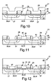
- Figures 5-12 are cross-sectional views similar to that of Figure 4 in successive steps of the manufacturing process;
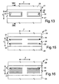
- Figure 13 is a top plan view similar to that of Figure 3, corresponding to a process for manufacturing a MOS device according to a different embodiment of the present invention;
- Figure 14 is a cross-sectional view of the wafer of semiconductor material taken along the line XIV-XIV of Figure 13, in a final step of the manufacturing process of the MOS device; and
- Figures 15 and 16 are top plan views similar to that of Figure 3, corresponding to further embodiments of the present invention.
- In detail, with reference to Figure 2 (which, like the subsequent figures, is not drawn to scale), the process for manufacturing a VDMOS power device first envisages provision of a
wafer 21 of semiconductor material, preferably silicon, comprising a substrate 22 (illustrated only in Figure 2), heavily doped and having a first type of conductivity (for example, of an N+ type). Then, asemiconductor layer 23, having the same type of conductivity (in the example, of an N type) as thesubstrate 22, is formed, for example via an epitaxial growth, above thesubstrate 22. In a per se known manner which is not described in detail, edge termination structures (not shown) of the VDMOS device are formed, and consequently an active area is defined wherein elementary functional units of the VDMOS device will be provided. - Then, a thin gate
dielectric layer 24, having for example a thickness less than 100 nm, is formed on thesemiconductor layer 23. The gatedielectric layer 24 can be formed via a thermal oxidation, or else via deposition of an oxynitride layer or of a multilayer constituted by successive layers of oxide, nitride, and oxide laid on top of one another. A gate-electrode layer 25, of polysilicon (intrinsic, or possibly doped), is deposited on the gatedielectric layer 24. Alternatively, a double layer formed by polysilicon and metallic silicide can be deposited. On the gate-electrode layer 25, a layer ofinsulating material 26 is then deposited, via CVD (Chemical Vapour Deposition). The layer ofinsulating material 26 can for example be of TEOS (Tetra-Ethyl-OrthoSilicate), USG (Undoped Silicon Glass), or PSG (Phosphosilicate Glass). - Next (see Figures 3 and 4), an
insulated gate structure 27 is defined using a photolithographic technique on thesemiconductor layer 23. In detail, through an appropriate masking, a one-directional etching of the layer ofinsulating material 26 is first performed with end-point on the gate-electrode layer 25, and then a one-directional etching of the gate-electrode layer 25 is performed for a pre-set time, or else with end-point on the gatedielectric layer 24. The resultinginsulated gate structure 27 comprises a plurality ofgate portions 28, which have a stripe-like shape and extend parallel to one another in a first direction x. Thegate portions 28 are constituted by the superposition of portions of the gatedielectric layer 24, of the gate-electrode layer 25 (in the following said portions will be referred to as gate electrodes 25), and of the layer ofinsulating material 26, and are separated by body/source windows 29 in a second direction y, orthogonal to the first direction x. The body/source windows 29 have a minor dimension L1 (in the following width L1) in the second direction y. The insulatedgate structure 27 further comprises connection elements (not shown) connecting thegate portions 28 in a comblike structure, of a type known for power devices. - According to an aspect of the present invention, simultaneously with the definition of the insulated
gate structure 27,enrichment windows 30 are opened within thegate portions 28, enabling access to portions of thesemiconductor layer 23 which are designed (as described in detail hereinafter) for the formation of intercell enrichment ion implants between adjacent elementary functional units of the VDMOS device. In particular, within eachgate portion 28, a plurality ofenrichment windows 30 is opened, said windows being aligned to one another in the first direction x, in a central position with respect to therespective gate portion 28. Theenrichment windows 30 have an approximately rectangular shape, with a major dimension 1 (in the following, length 1) in the first direction x, and a minor dimension L2 (in the following, width L2) in the second direction y. The width L2 of theenrichment windows 30 is smaller than the width L1 of the body/source windows 29; in particular, the ratio L1/L2 is preferably greater than or equal to 2. - In addition, the
enrichment windows 30 are separated from one another by a separation gap s, in the first direction x. In particular, the ratio between thelength 1 of theenrichment windows 30 and the separation gap s must be appropriately sized, taking into account the design and performance requirements of the VDMOS device, and in particular the switching speed, which depends upon the resistance of theinsulated gate structure 27 and upon the distributed capacitance between theinsulated gate structure 27 and the electrodes of the VDMOS device (source, body and drain). In fact, the interruption of the gate-electrode layer 25 affects both the resistance of the gate electrode and the distribution of the gate electric field in the proximity of theenrichment windows 30. - The manufacturing process proceeds (see Figure 5) with the deposition of a thin silicon-
nitride layer 34, having, for example, a thickness smaller than 50 nm, and a high degree of conformality. On top of the silicon-nitride layer 34 a layer ofsacrificial material 35 is then deposited, constituted by polysilicon, either intrinsic or doped. In particular, the thickness of the layer ofsacrificial material 35 is greater than the half-width of the enrichment windows 30 (i.e., greater than L2/2). - Next (Figure 6), a wet etching of the layer of
sacrificial material 35 is performed, until the silicon-nitride layer 34 within the body/source windows 29 is exposed. At the end of the etching, eachenrichment window 30 remains filled by afirst barrier region 36, constituted by a remaining portion of the layer ofsacrificial material 35. In particular, the maximum value of the width L2 of theenrichment windows 30 must be such as to enable a filling by thefirst barrier region 36 to be obtained during the aforesaid etching step. The maximum value of the width L2 is, for example, in the region of 1 µm. The minimum value of the width L2 is instead determined by the technological limits of the photo-exposure technique used for the formation of theenrichment windows 30; for example, said minimum value is currently 0.25 µm. - Subsequently (Figure 7), a one-directional (dry) etching of the silicon-
nitride layer 34 is performed, for a pre-set time or else with end-point on thegate dielectric layer 24, and possibly a further one-directional etching of thegate dielectric layer 24. A first ion implantation is then performed, self-aligned with respect to the body/source windows 29, to obtainbody wells 37 within thesemiconductor layer 23. After a thermal diffusion process of thebody wells 37, a second ion implantation is performed to obtainsource regions 38 within thebody wells 37. In particular, the first ion implantation has a type of conductivity opposite to that of the semiconductor layer 23 (in the example, of a P type), whilst the second ion implantation has a type of conductivity opposite to that of the first ion implantation (in the example, of an N+ type). It should be noted, in particular, that the first and second ion implants are blocked within theenrichment windows 30 by thefirst barrier region 36. - Then (Figure 8), a photoresist layer is deposited and etched to form a
mask 40, which entirely covers the body/source windows 29 and leaves, instead, exposed theenrichment windows 30. A wet etching of the first barrier regions 36 (possibly preceded by a slight etching of the first dielectric layer 26), and a dry etching of the underlying silicon-nitride layer 34, and optionally of thegate dielectric layer 24, are then performed. Themask 40 protects the body/source windows 29 from the aforesaid etching. - The subsequent process step (see Figure 9) envisages a self-aligned ion implantation through the
enrichment windows 30, following upon whichenrichment regions 42 are formed having the same type of conductivity as the semiconductor layer 23 (in the example, of an N type). In particular, theenrichment regions 42 have the function of increasing the conductivity of the regions of thesemiconductor layer 23 arranged between adjacent body wells 37 (drift regions) in order to reduce the ON-resistance Rdson of the VDMOS device. In this step, themask 40 protects the body/source windows 29 from the ion implantation. Themask 40 is then removed, and a diffusion of theenrichment region 42 is performed via an appropriate thermal process. - Next (see Figure 10) a CVD deposition of a
filler layer 43 is performed, thefiller layer 43 being of a dielectric material with low conformality, the thickness of which depending upon the planar geometry of the VDMOS device; the dielectric material can be USG, PSG, TEOS, or any other dielectric or dielectric multilayer. - After a densification step of the
filler layer 43, a one-directional etching thereof is performed (Figure 11), with end-point on thesemiconductor layer 23. Following upon said etching, twoinsulation spacers 44 at the edges of each body/source window 29 are formed, in a position adjacent to therespective gate portions 28. Theenrichment windows 30 remain filled with aninsulation region 45, constituted by a remaining portion of thefiller layer 43. - Next (see Figure 12), a layer of
metallic material 46 is formed on thewafer 21, having the function of contacting thesource regions 38. Interruptions (not shown) of thesource regions 38 are provided in the first direction x, in such a way that the layer ofmetallic material 46 contacts also thebody wells 37. The insulation spacers 44 electrically insulate from one another the layer ofmetallic material 46 and thegate electrodes 25. The ratio between the thickness of thefiller layer 43 and the width L1 of the source/body windows 29 is to be sized (generally maximized) so as to obtain a robust and homogeneous lateral insulation of thegate electrodes 25. For example, the value of said ratio is comprised between 0.1 and 0.2. - The manufacturing process of the VDMOS device terminates with the preparation and metallization of the back of the
wafer 21 to provide a drain electrical contact. - According to a different embodiment of the present invention, illustrated in Figures 13 and 14, the enrichment windows 30 (and consequently the enrichment regions 42) have a different shape, in particular the shape of a rectangular annulus. Said embodiment is advantageous in VDMOS devices in which the distance between
adjacent body wells 37 must be kept wide to reduce the J-FET contribution in the ON-resistance Rdson. In fact, using the first embodiment described, theenrichment regions 42, provided for reasons of symmetry in the proximity of the centre of thegate portions 28, would be too distant from the terminations of the conduction channel of the VDMOS device to cause a significant reduction in the ON-resistance Rdson. Instead, in the case ofenrichment windows 30 having the shape of a rectangular annulus, the width of the windows is still compatible with the need for self-alignment of theenrichment regions 42, and at the same time the distance between theenrichment regions 42 and the channel terminations is sufficiently small as to guarantee a considerable reduction in the ON-resistance Rdson. The definition of theenrichment windows 30, in this case brings about the formation ofislands 48, which are physically separated from thegate electrode 25 and so cannot be directly biased. This leads to a reduction in the capacitance between thegate electrode 25 and the drain and in the charging time of thegate electrode 25. At the same time, there is no excessive alteration in the property of "field plating", which normally thegate electrode 25 exerts on the distribution of the drain electric field in the active region of the VDMOS device. - According to a further embodiment of the present invention, illustrated in Figure 15, a plurality of pairs of
enrichment windows 30, aligned in the first direction x, is defined within eachgate portion 28. Theenrichment windows 30 of each pair are rectangular, parallel to one another and to the first direction x and aligned in the second direction y; in addition, theenrichment windows 30 are provided in the proximity of the channel regions of the VDMOS device. In particular, theenrichment windows 30 are arranged symmetrically with respect to a central axis of therespective gate portion 28 extending in the first direction x. - A further embodiment, illustrated in Figure 16, envisages the formation, within each
gate portion 28, of a plurality of grids ofenrichment windows 30 aligned in the first direction x. Theenrichment windows 30 within each grid are rectangular and parallel to one another and to the first direction x, and are aligned in the second direction y and arranged symmetrically with respect to a central axis of therespective gate portion 28, extending in the first direction x. Said embodiment leads to an increase in the planar resistance of thegate electrode 25, but to a decrease in the ON-resistance Rdson, due to the presence of a number ofenrichment regions 42. - The advantages of the described manufacturing process are clear from the foregoing description.
- In particular, thanks to the self-aligned ion implantations through the enrichment windows, the alignment of the intercell enrichment regions with respect to the body and source diffusions is automatic and guaranteed, without the need for definition of purposely provided masks. In this way, the process for manufacturing the VDMOS device may be freed from the technological limits of the photolithographic processes, above all as regards highly scaled technologies.
- The enrichment regions enable a marked reduction in the ON-resistance of the VDMOS device, and at the same time characteristics such as planar resistance and gate capacitance are not significantly altered, without any consequent modification in the switching speed of the VDMOS device.
- Finally, it is clear that modifications and variations may be made to what is described and illustrated herein, without thereby departing from the scope of the present invention, as defined in the attached claims.
- In particular, the gate and source/body electrical contacts can be defined with photolithographic technique, i.e., without self-aligned formation of the insulation spacers in the body/source windows. In this case, the second layer of dielectric material does not necessarily have a low conformality, and must have a thickness greater than the half-width of the enrichment window. The corresponding process steps envisage deposition of the second layer of dielectric material, densification thereof, and then photolithography of the contacts, in a way in itself known and hence not described in detail herein.
- In addition, the shape and the number of the enrichment windows could be different from what has been described and illustrated.
- In addition, it is clear that the described process may be advantageously applied to other MOS devices, such as for example signal VDMOSs, IGBTs, MOSFETs, whether N-channel or P-channel, with edge terminations of any shape and size, and any configuration of the cells in the active area (for example, hexagonal or square). In addition, even though the entire description has been made with reference to the case of a P-channel VDMOS device, extension to the dual case corresponding to an N-channel VDMOS device is immediate.
- Finally, the described process can advantageously be applied for forming any kind of ion implant in the intercell region.
Claims (15)
- A process for manufacturing a MOS device, comprising:- forming a semiconductor layer (23) having a first type of conductivity;- forming an insulated gate structure (27) comprising an electrode region (25) above said semiconductor layer (23);- forming body regions (37), having a second type of conductivity, within said semiconductor layer (23) laterally and partially underneath said insulated gate structure (27);- forming source regions (38) having said first type of conductivity within said body regions (37); and- forming a first enrichment region (42) in a surface portion of said semiconductor layer (23) underneath said insulated gate structure (27), said first enrichment region (42) having said first type of conductivity and being set at a distance from said body regions (37),characterized in that forming a first enrichment region (42) comprises:- defining a first enrichment window (30) within said insulated gate structure (27); and- introducing first dopant species of said first type of conductivity through, and in a way self-aligned to, said first enrichment window (30).
- The process according to claim 1, wherein forming an insulated gate structure (27) comprises:- forming a first layer of dielectric material (24) on said semiconductor layer (23);- depositing a layer of conductive material (25) on said first layer of dielectric material (24); and- selectively removing a first portion of said first layer of conductive material (25), thereby forming said insulated gate structure (27),
and wherein defining a first enrichment window (30) comprises selectively removing a second portion of said first layer of conductive material (25) within said insulated gate structure (27); said selectively removing a first portion and selectively removing a second portion being executed simultaneously. - The process according to claim 1 or 2, wherein said insulated gate structure (27) comprises at least two gate portions (28) separated by a body/source window (29) in a transverse direction (y), said first enrichment window (30) and said body/source window (29) having a respective dimension (L2, L1) in said transverse direction (y); the ratio (L1/L2) between the respective dimensions of said body/source window (29) and of said first enrichment window (30) being not less than two.
- The process according to claim 3, further comprising:- defining at least one second enrichment window (30) within said insulated gate structure (27) and simultaneously to said first enrichment window (30); and- forming at least one second enrichment region (42) through said second enrichment window (30), simultaneously to said first enrichment region (42),said first and said second enrichment windows (30) having an approximately rectangular shape, and being formed within at least one of said two gate portions (28) of said insulated gate structure (27).
- The process according to claim 4, wherein said first enrichment window (30) and said second enrichment window (30) are aligned to one another in at least one direction of alignment chosen between said transverse direction (y) and a direction (x) perpendicular to said transverse direction (y).
- The process according to claim 3, further comprising:- defining at least one second enrichment window (30) within said insulated gate structure (27) and simultaneously to said first enrichment window (30); and- forming at least one second enrichment region (42) through said second enrichment window (30), simultaneously to said first enrichment region (42),said first and said second enrichment windows (30) having approximately the shape of a rectangular annulus, being formed within at least one of said two gate portions (28) of said insulated gate structure (27), and being aligned to one another in said transverse direction (y).
- The process according to any one of claims 3-6, wherein forming body regions (37) comprises the steps of:- depositing a layer of sacrificial material (35) on said semiconductor layer (23);- etching said layer of sacrificial material (35) so as to remove it completely from said body/source window (29), and to leave a portion thereof forming a barrier region (36) within said first enrichment window (30); and- introducing second dopant species of said second type of conductivity through said body/source window (29) in the presence of said barrier region (36).
- The process according to claim 7, wherein said layer of sacrificial material (35) has a thickness not lower than half of said dimension (L2) of said enrichment window (30), and said layer of sacrificial material (35) is made of polysilicon.
- The process according to claim 7 or 8, wherein forming an enrichment region (42) comprises, prior to introducing first dopant species:- covering said body/source window (29) with a mask (40); and- removing said barrier region (36);introducing first dopant species being performed in the presence of said mask (40).
- The process according to any one of claims 3-9, further comprising:- depositing a second layer of dielectric material (43) above said semiconductor layer (23);- etching said second layer of dielectric material (43) so as to form insulation spacers (44) within said body/source window (29) and an insulation region (45) within said first enrichment window (30).
- A MOS device, comprising:- a semiconductor layer (23) having a first type of conductivity;- an insulated gate structure (27) formed above said semiconductor layer (23), and comprising a first region of dielectric material (24) and an electrode region (25);- body regions (37) having a second type of conductivity, formed within said semiconductor layer (23), laterally and partially underneath said insulated gate structure (27);- source regions (38) having said first type of conductivity, formed within said body regions (37); and- a first enrichment region (42) formed in a surface portion of said semiconductor layer (23) arranged underneath said insulated gate structure (27), said first enrichment region (42) having said first type of conductivity and being set at a distance from said body regions (37),characterized in that said electrode region (25) has a first opening (30) overlying said first enrichment region (42) and filled at least partially with dielectric material.
- The device according to claim 11, wherein said insulated gate structure (27) comprises at least two gate portions (28) separated by a body/source window (29) in a transverse direction (y), said first opening (30) and said body/source window (29) having a respective dimension (L2, L1) in said transverse direction (y); the ratio (L1/L2) between the respective dimensions of said body/source window (29) and of said first opening (30) being not less than two.
- The device according to claim 12, wherein said first opening (30) is formed in a first of said two gate portions (28), and said first gate portion (28) further has at least one second opening (30) filled at least partially with dielectric material and overlying a second enrichment region (42) formed in said semiconductor layer (23), said first and said second openings (30) having an approximately rectangular shape.
- The device according to claim 13, wherein said first and second openings (30) are aligned to one another in at least one direction of alignment chosen between said transverse direction (y) and a direction (x) perpendicular to said transverse direction (y).
- The device according to claim 13 or 14, wherein said first and second openings (30) have approximately the shape of a rectangular annulus, and are filled completely with dielectric material; each one of said first and second openings (30) surrounding a respective island (48) of conductive material.
Priority Applications (4)
| Application Number | Priority Date | Filing Date | Title |
|---|---|---|---|
| EP05425260A EP1717849A1 (en) | 2005-04-27 | 2005-04-27 | Process for manufacturing a MOS device with intercell ion implant |
| PCT/EP2006/061664 WO2006114376A1 (en) | 2005-04-27 | 2006-04-19 | Process for manufacturing a mos device with intercell ion implant |
| US11/919,570 US8158463B2 (en) | 2005-04-27 | 2006-04-19 | Process and method for manufacturing a MOS device with intercell ion implant using one or more parallel enrichment windows |
| US13/292,003 US8324669B2 (en) | 2005-04-27 | 2011-11-08 | Process for manufacturing a MOS device with intercell ion implant confined to the gate electrode region |
Applications Claiming Priority (1)
| Application Number | Priority Date | Filing Date | Title |
|---|---|---|---|
| EP05425260A EP1717849A1 (en) | 2005-04-27 | 2005-04-27 | Process for manufacturing a MOS device with intercell ion implant |
Publications (1)
| Publication Number | Publication Date |
|---|---|
| EP1717849A1 true EP1717849A1 (en) | 2006-11-02 |
Family
ID=35768598
Family Applications (1)
| Application Number | Title | Priority Date | Filing Date |
|---|---|---|---|
| EP05425260A Withdrawn EP1717849A1 (en) | 2005-04-27 | 2005-04-27 | Process for manufacturing a MOS device with intercell ion implant |
Country Status (3)
| Country | Link |
|---|---|
| US (2) | US8158463B2 (en) |
| EP (1) | EP1717849A1 (en) |
| WO (1) | WO2006114376A1 (en) |
Families Citing this family (5)
| Publication number | Priority date | Publication date | Assignee | Title |
|---|---|---|---|---|
| ITTO20070163A1 (en) | 2007-03-02 | 2008-09-03 | St Microelectronics Srl | PROCESS OF MANUFACTURING A MISFET VERTICAL CONDUCTIVE DEVICE WITH DIELECTRIC STRUCTURE OF DOOR OF DIFFERENTIAL THICKNESS AND MISFET DEVICE WITH A VERTICAL CONDUCTION MADE THESE |
| CN103855034A (en) * | 2014-03-03 | 2014-06-11 | 宁波达新半导体有限公司 | Method for manufacturing MOS grid device |
| CN105990152B (en) * | 2015-03-03 | 2019-05-07 | 北大方正集团有限公司 | A kind of VDMOS device and its manufacturing method |
| CN111009471A (en) * | 2019-12-25 | 2020-04-14 | 爱特微(张家港)半导体技术有限公司 | A kind of preparation method of MOSFET power semiconductor device |
| CN110957371A (en) * | 2019-12-31 | 2020-04-03 | 无锡麟力科技有限公司 | Low-on-resistance medium-low flat-surface gate VDMOS device and manufacturing process thereof |
Citations (5)
| Publication number | Priority date | Publication date | Assignee | Title |
|---|---|---|---|---|
| JPH05299658A (en) * | 1992-04-20 | 1993-11-12 | Nec Kansai Ltd | Semiconductor device and manufacture thereof |
| JPH07221296A (en) * | 1994-01-28 | 1995-08-18 | Sanyo Electric Co Ltd | Vertical MOS semiconductor device and manufacturing method thereof |
| JPH09102506A (en) * | 1995-10-05 | 1997-04-15 | Hitachi Ltd | Method for manufacturing semiconductor device |
| JPH10335643A (en) * | 1997-06-05 | 1998-12-18 | Toshiba Corp | Method for manufacturing semiconductor device |
| EP1313147A2 (en) * | 2001-11-14 | 2003-05-21 | Kabushiki Kaisha Toshiba | Power MOSFET device |
Family Cites Families (14)
| Publication number | Priority date | Publication date | Assignee | Title |
|---|---|---|---|---|
| US4199774A (en) * | 1978-09-18 | 1980-04-22 | The Board Of Trustees Of The Leland Stanford Junior University | Monolithic semiconductor switching device |
| JPS5553462A (en) * | 1978-10-13 | 1980-04-18 | Int Rectifier Corp | Mosfet element |
| US4974059A (en) * | 1982-12-21 | 1990-11-27 | International Rectifier Corporation | Semiconductor high-power mosfet device |
| US5273922A (en) | 1992-09-11 | 1993-12-28 | Motorola, Inc. | High speed, low gate/drain capacitance DMOS device |
| US5869371A (en) | 1995-06-07 | 1999-02-09 | Stmicroelectronics, Inc. | Structure and process for reducing the on-resistance of mos-gated power devices |
| US6049104A (en) * | 1997-11-28 | 2000-04-11 | Magepower Semiconductor Corp. | MOSFET device to reduce gate-width without increasing JFET resistance |
| EP0936674B1 (en) * | 1998-02-10 | 2006-04-26 | STMicroelectronics S.r.l. | Integrated circuit comprising a VDMOS transistor protected against overvoltages between source and gate |
| KR100854078B1 (en) * | 2001-09-12 | 2008-08-25 | 페어차일드코리아반도체 주식회사 | Morse gate type power semiconductor device and manufacturing method thereof |
| US7067363B2 (en) * | 2002-12-30 | 2006-06-27 | Stmicroelectronics S.R.L. | Vertical-conduction and planar-structure MOS device with a double thickness of gate oxide and method for realizing power vertical MOS transistors with improved static and dynamic performances and high scaling down density |
| EP1455397A3 (en) | 2002-12-30 | 2005-08-17 | STMicroelectronics S.r.l. | Vertical MOS device and method of making the same |
| US20040164346A1 (en) * | 2003-02-20 | 2004-08-26 | Semiconductor Components Industries, Llc. | Power switching transistor with low drain to gate capacitance |
| US6992353B1 (en) * | 2004-11-01 | 2006-01-31 | Silicon-Based Technology Corp. | Self-aligned source structure of planar DMOS power transistor and its manufacturing methods |
| US7382594B2 (en) * | 2005-09-21 | 2008-06-03 | Semiconductor Components Industries, Llc | Method of forming an integrated voltage protection device and structure |
| ITTO20070163A1 (en) * | 2007-03-02 | 2008-09-03 | St Microelectronics Srl | PROCESS OF MANUFACTURING A MISFET VERTICAL CONDUCTIVE DEVICE WITH DIELECTRIC STRUCTURE OF DOOR OF DIFFERENTIAL THICKNESS AND MISFET DEVICE WITH A VERTICAL CONDUCTION MADE THESE |
-
2005
- 2005-04-27 EP EP05425260A patent/EP1717849A1/en not_active Withdrawn
-
2006
- 2006-04-19 US US11/919,570 patent/US8158463B2/en active Active
- 2006-04-19 WO PCT/EP2006/061664 patent/WO2006114376A1/en not_active Ceased
-
2011
- 2011-11-08 US US13/292,003 patent/US8324669B2/en not_active Expired - Lifetime
Patent Citations (5)
| Publication number | Priority date | Publication date | Assignee | Title |
|---|---|---|---|---|
| JPH05299658A (en) * | 1992-04-20 | 1993-11-12 | Nec Kansai Ltd | Semiconductor device and manufacture thereof |
| JPH07221296A (en) * | 1994-01-28 | 1995-08-18 | Sanyo Electric Co Ltd | Vertical MOS semiconductor device and manufacturing method thereof |
| JPH09102506A (en) * | 1995-10-05 | 1997-04-15 | Hitachi Ltd | Method for manufacturing semiconductor device |
| JPH10335643A (en) * | 1997-06-05 | 1998-12-18 | Toshiba Corp | Method for manufacturing semiconductor device |
| EP1313147A2 (en) * | 2001-11-14 | 2003-05-21 | Kabushiki Kaisha Toshiba | Power MOSFET device |
Non-Patent Citations (4)
| Title |
|---|
| PATENT ABSTRACTS OF JAPAN vol. 018, no. 095 (E - 1509) 16 February 1994 (1994-02-16) * |
| PATENT ABSTRACTS OF JAPAN vol. 1995, no. 11 26 December 1995 (1995-12-26) * |
| PATENT ABSTRACTS OF JAPAN vol. 1997, no. 08 29 August 1997 (1997-08-29) * |
| PATENT ABSTRACTS OF JAPAN vol. 1999, no. 03 31 March 1999 (1999-03-31) * |
Also Published As
| Publication number | Publication date |
|---|---|
| WO2006114376A1 (en) | 2006-11-02 |
| US20090315102A1 (en) | 2009-12-24 |
| US8324669B2 (en) | 2012-12-04 |
| US20120139034A1 (en) | 2012-06-07 |
| US8158463B2 (en) | 2012-04-17 |
Similar Documents
| Publication | Publication Date | Title |
|---|---|---|
| US11075297B2 (en) | Semiconductor device and method of manufacturing semiconductor device | |
| US10608092B2 (en) | Semiconductor power devices manufactured with self-aligned processes and more reliable electrical contacts | |
| US8779510B2 (en) | Semiconductor power devices manufactured with self-aligned processes and more reliable electrical contacts | |
| KR100415490B1 (en) | Power mos element and method for producing the same | |
| US5879994A (en) | Self-aligned method of fabricating terrace gate DMOS transistor | |
| US12148824B2 (en) | MOSFET device with shielding region and manufacturing method thereof | |
| US8541839B2 (en) | Semiconductor component and method for producing it | |
| EP2043158A2 (en) | Trench DMOS transistor with trench bottom implant | |
| US20030020115A1 (en) | Power MOSFET with ultra-deep base and reduced on resistance | |
| EP4231361B1 (en) | Method for auto-aligned manufacturing of a trench-gate mos transistor, and shielded-gate mos transistor | |
| US20040104427A1 (en) | Dense trench MOSFET with decreased etch sensitivity to deposition and etch processing | |
| US8324669B2 (en) | Process for manufacturing a MOS device with intercell ion implant confined to the gate electrode region | |
| US6756644B2 (en) | Ultra low QGD power MOSFET | |
| EP1162665A2 (en) | Trench gate MIS device and method of fabricating the same | |
| EP0961325B1 (en) | High integration density MOS technology power device | |
| US20240136411A1 (en) | Transistor device and method of fabricating contacts to a semiconductor substrate | |
| WO2007036793A2 (en) | Power mosfets and methods of making same | |
| EP4421877A1 (en) | Semiconductor die and method of manufacturing the same | |
| WO2006122957A2 (en) | Mos power device with high integration density and manufacturing process thereof |
Legal Events
| Date | Code | Title | Description |
|---|---|---|---|
| PUAI | Public reference made under article 153(3) epc to a published international application that has entered the european phase |
Free format text: ORIGINAL CODE: 0009012 |
|
| AK | Designated contracting states |
Kind code of ref document: A1 Designated state(s): AT BE BG CH CY CZ DE DK EE ES FI FR GB GR HU IE IS IT LI LT LU MC NL PL PT RO SE SI SK TR |
|
| AX | Request for extension of the european patent |
Extension state: AL BA HR LV MK YU |
|
| 17P | Request for examination filed |
Effective date: 20070430 |
|
| AKX | Designation fees paid |
Designated state(s): DE FR GB IT |
|
| 17Q | First examination report despatched |
Effective date: 20080721 |
|
| RAP1 | Party data changed (applicant data changed or rights of an application transferred) |
Owner name: STMICROELECTRONICS SRL |
|
| STAA | Information on the status of an ep patent application or granted ep patent |
Free format text: STATUS: THE APPLICATION IS DEEMED TO BE WITHDRAWN |
|
| 18D | Application deemed to be withdrawn |
Effective date: 20110601 |