EP1716341B1 - Wälzlager mit einem system zur datenerfassung und zur datenverarbeitung - Google Patents
Wälzlager mit einem system zur datenerfassung und zur datenverarbeitung Download PDFInfo
- Publication number
- EP1716341B1 EP1716341B1 EP04802815A EP04802815A EP1716341B1 EP 1716341 B1 EP1716341 B1 EP 1716341B1 EP 04802815 A EP04802815 A EP 04802815A EP 04802815 A EP04802815 A EP 04802815A EP 1716341 B1 EP1716341 B1 EP 1716341B1
- Authority
- EP
- European Patent Office
- Prior art keywords
- friction bearing
- carrier
- layers
- layer
- elements
- Prior art date
- Legal status (The legal status is an assumption and is not a legal conclusion. Google has not performed a legal analysis and makes no representation as to the accuracy of the status listed.)
- Expired - Lifetime
Links
- 238000012545 processing Methods 0.000 title claims abstract description 12
- 238000013480 data collection Methods 0.000 title abstract 2
- 239000004020 conductor Substances 0.000 claims abstract description 17
- 239000000919 ceramic Substances 0.000 claims description 20
- 239000010408 film Substances 0.000 claims description 11
- 238000000034 method Methods 0.000 claims description 11
- 239000000758 substrate Substances 0.000 claims description 7
- 239000010409 thin film Substances 0.000 claims description 7
- 229910010293 ceramic material Inorganic materials 0.000 claims description 4
- 239000000835 fiber Substances 0.000 claims description 2
- 238000002347 injection Methods 0.000 claims 1
- 239000007924 injection Substances 0.000 claims 1
- 239000010410 layer Substances 0.000 description 90
- 238000005096 rolling process Methods 0.000 description 37
- 239000000463 material Substances 0.000 description 7
- 239000007788 liquid Substances 0.000 description 6
- 229910000679 solder Inorganic materials 0.000 description 5
- 238000013461 design Methods 0.000 description 4
- 238000005516 engineering process Methods 0.000 description 4
- 239000012530 fluid Substances 0.000 description 4
- BASFCYQUMIYNBI-UHFFFAOYSA-N platinum Chemical compound [Pt] BASFCYQUMIYNBI-UHFFFAOYSA-N 0.000 description 4
- 241001295925 Gegenes Species 0.000 description 3
- 239000012876 carrier material Substances 0.000 description 3
- 238000011156 evaluation Methods 0.000 description 3
- 229910052751 metal Inorganic materials 0.000 description 3
- 239000002184 metal Substances 0.000 description 3
- 239000007769 metal material Substances 0.000 description 3
- 239000000843 powder Substances 0.000 description 3
- KDLHZDBZIXYQEI-UHFFFAOYSA-N Palladium Chemical compound [Pd] KDLHZDBZIXYQEI-UHFFFAOYSA-N 0.000 description 2
- BQCADISMDOOEFD-UHFFFAOYSA-N Silver Chemical compound [Ag] BQCADISMDOOEFD-UHFFFAOYSA-N 0.000 description 2
- 239000011230 binding agent Substances 0.000 description 2
- 230000005540 biological transmission Effects 0.000 description 2
- 239000003990 capacitor Substances 0.000 description 2
- 239000011521 glass Substances 0.000 description 2
- 239000002241 glass-ceramic Substances 0.000 description 2
- PCHJSUWPFVWCPO-UHFFFAOYSA-N gold Chemical compound [Au] PCHJSUWPFVWCPO-UHFFFAOYSA-N 0.000 description 2
- 229910052737 gold Inorganic materials 0.000 description 2
- 239000010931 gold Substances 0.000 description 2
- 239000012212 insulator Substances 0.000 description 2
- 238000004519 manufacturing process Methods 0.000 description 2
- 229910044991 metal oxide Inorganic materials 0.000 description 2
- 150000004706 metal oxides Chemical class 0.000 description 2
- 239000000203 mixture Substances 0.000 description 2
- 229910052697 platinum Inorganic materials 0.000 description 2
- 230000035939 shock Effects 0.000 description 2
- 229910052709 silver Inorganic materials 0.000 description 2
- 239000004332 silver Substances 0.000 description 2
- 238000005476 soldering Methods 0.000 description 2
- 238000003860 storage Methods 0.000 description 2
- 239000000126 substance Substances 0.000 description 2
- 238000003466 welding Methods 0.000 description 2
- ZEMPKEQAKRGZGQ-AAKVHIHISA-N 2,3-bis[[(z)-12-hydroxyoctadec-9-enoyl]oxy]propyl (z)-12-hydroxyoctadec-9-enoate Chemical compound CCCCCCC(O)C\C=C/CCCCCCCC(=O)OCC(OC(=O)CCCCCCC\C=C/CC(O)CCCCCC)COC(=O)CCCCCCC\C=C/CC(O)CCCCCC ZEMPKEQAKRGZGQ-AAKVHIHISA-N 0.000 description 1
- 229910021364 Al-Si alloy Inorganic materials 0.000 description 1
- 229910001020 Au alloy Inorganic materials 0.000 description 1
- OKTJSMMVPCPJKN-UHFFFAOYSA-N Carbon Chemical compound [C] OKTJSMMVPCPJKN-UHFFFAOYSA-N 0.000 description 1
- RYGMFSIKBFXOCR-UHFFFAOYSA-N Copper Chemical compound [Cu] RYGMFSIKBFXOCR-UHFFFAOYSA-N 0.000 description 1
- KJTLSVCANCCWHF-UHFFFAOYSA-N Ruthenium Chemical compound [Ru] KJTLSVCANCCWHF-UHFFFAOYSA-N 0.000 description 1
- 229910004298 SiO 2 Inorganic materials 0.000 description 1
- 229910000831 Steel Inorganic materials 0.000 description 1
- 229910010413 TiO 2 Inorganic materials 0.000 description 1
- 230000001133 acceleration Effects 0.000 description 1
- 230000006978 adaptation Effects 0.000 description 1
- 239000000853 adhesive Substances 0.000 description 1
- 238000004026 adhesive bonding Methods 0.000 description 1
- 230000001070 adhesive effect Effects 0.000 description 1
- 229910045601 alloy Inorganic materials 0.000 description 1
- 239000000956 alloy Substances 0.000 description 1
- 238000004364 calculation method Methods 0.000 description 1
- 229910052799 carbon Inorganic materials 0.000 description 1
- 239000000969 carrier Substances 0.000 description 1
- 239000003795 chemical substances by application Substances 0.000 description 1
- VNNRSPGTAMTISX-UHFFFAOYSA-N chromium nickel Chemical compound [Cr].[Ni] VNNRSPGTAMTISX-UHFFFAOYSA-N 0.000 description 1
- 238000004891 communication Methods 0.000 description 1
- 150000001875 compounds Chemical class 0.000 description 1
- 239000000470 constituent Substances 0.000 description 1
- 238000010276 construction Methods 0.000 description 1
- 238000001816 cooling Methods 0.000 description 1
- 229910052802 copper Inorganic materials 0.000 description 1
- 239000010949 copper Substances 0.000 description 1
- HTXDPTMKBJXEOW-UHFFFAOYSA-N dioxoiridium Chemical compound O=[Ir]=O HTXDPTMKBJXEOW-UHFFFAOYSA-N 0.000 description 1
- 238000009826 distribution Methods 0.000 description 1
- 230000005489 elastic deformation Effects 0.000 description 1
- 230000007613 environmental effect Effects 0.000 description 1
- 239000000945 filler Substances 0.000 description 1
- 230000017525 heat dissipation Effects 0.000 description 1
- 238000009434 installation Methods 0.000 description 1
- 229910000457 iridium oxide Inorganic materials 0.000 description 1
- 230000001050 lubricating effect Effects 0.000 description 1
- 229910052749 magnesium Inorganic materials 0.000 description 1
- 238000002844 melting Methods 0.000 description 1
- 230000008018 melting Effects 0.000 description 1
- 150000002739 metals Chemical class 0.000 description 1
- 239000003607 modifier Substances 0.000 description 1
- 229910001120 nichrome Inorganic materials 0.000 description 1
- HBEQXAKJSGXAIQ-UHFFFAOYSA-N oxopalladium Chemical compound [Pd]=O HBEQXAKJSGXAIQ-UHFFFAOYSA-N 0.000 description 1
- 229910052763 palladium Inorganic materials 0.000 description 1
- 229910003445 palladium oxide Inorganic materials 0.000 description 1
- 238000002161 passivation Methods 0.000 description 1
- 239000010970 precious metal Substances 0.000 description 1
- 238000003825 pressing Methods 0.000 description 1
- 238000007639 printing Methods 0.000 description 1
- 239000011241 protective layer Substances 0.000 description 1
- 229910052707 ruthenium Inorganic materials 0.000 description 1
- 238000007650 screen-printing Methods 0.000 description 1
- 238000007789 sealing Methods 0.000 description 1
- 239000004065 semiconductor Substances 0.000 description 1
- 230000008054 signal transmission Effects 0.000 description 1
- 238000005245 sintering Methods 0.000 description 1
- 239000010959 steel Substances 0.000 description 1
- 229920003002 synthetic resin Polymers 0.000 description 1
- 239000000057 synthetic resin Substances 0.000 description 1
- 229910052725 zinc Inorganic materials 0.000 description 1
Images




Classifications
-
- G—PHYSICS
- G01—MEASURING; TESTING
- G01L—MEASURING FORCE, STRESS, TORQUE, WORK, MECHANICAL POWER, MECHANICAL EFFICIENCY, OR FLUID PRESSURE
- G01L5/00—Apparatus for, or methods of, measuring force, work, mechanical power, or torque, specially adapted for specific purposes
- G01L5/0009—Force sensors associated with a bearing
- G01L5/0019—Force sensors associated with a bearing by using strain gages, piezoelectric, piezo-resistive or other ohmic-resistance based sensors
-
- G—PHYSICS
- G01—MEASURING; TESTING
- G01L—MEASURING FORCE, STRESS, TORQUE, WORK, MECHANICAL POWER, MECHANICAL EFFICIENCY, OR FLUID PRESSURE
- G01L5/00—Apparatus for, or methods of, measuring force, work, mechanical power, or torque, specially adapted for specific purposes
- G01L5/0009—Force sensors associated with a bearing
Definitions
- the invention relates to a rolling bearing with a system for data acquisition and data processing, wherein the system is fixed to the rolling bearing and at least one sensor element for detecting physical quantities, conductor elements and electronic components.
- a rolling bearing to which sensors are attached for determining physical quantities.
- the sensors are designed as strain gauges and preferably mounted in a groove on the circumference of one of the bearing rings. These strain gauges are applied via an insulating layer on a metallic intermediate carrier.
- Another carrier material is designed as a circuit carrier and surrounds the metallic Intermediate carrier with the strain gauges.
- the circuit carrier accommodates electronic components and printed conductors. The intermediate carrier layer and the circuit carrier layer are pressed into the groove on the bearing ring or welded to the groove.
- DE 101 36 438 A1 are described as full or half-bridge circuits Dehnmesswiderrange on a metallic intermediate carrier described.
- DE 101 36 438 A1 electronic components for the evaluation of the sensor signals and for the transmission of these to other measuring points or to a connector or to a circuit for the evaluation of the signals.
- the transmission of the signals in this bearing is done via digital or analog bus systems, for example in a motor vehicle.
- the groove for receiving the above-described system for data acquisition and data processing must be taken into account in the design of the bearing ring and thus also of the rolling bearing.
- a rolling bearing without such a system is not readily interchangeable with a construction and size same bearing equipped with this system, since the groove for receiving the system can weaken the corresponding bearing ring considerably.
- Measuring bearings in the design of the prior art are therefore not always interchangeable with size-identical bearings without measuring device, d.
- a rolling bearing with a corresponding system is generally larger in size and can therefore be fitted only after changing the surrounding structure in an existing system.
- WO 02/054031 A1 describes a system for data acquisition on a shaft, roll on the rolling elements, wherein on the shaft, a high-resistance layer, on this a structured low-ohmic layer for contacts and printed conductors, and on this turn a piezoresistive measuring layer is formed.
- the layers mentioned are made of diamond-like carbon (DLC) which are suitably doped.
- DLC diamond-like carbon
- the system with the three layers is firmly connected to the body of the shaft and applied to the shaft via a CVD process.
- the document further describes the possibility of providing temperature sensors in addition to the pressure sensors in order to detect the temperature in the region of the measuring layer and to be able to eliminate the influence of the temperature on the detected measured value by calculation. The problem of mechanical adjustment of the measuring system to the material of the shaft at higher temperatures is not eliminated.
- EP 1 148 261 A2 describes a rolling bearing having a system for detecting forces, the system comprising SAW or BAW sensors arranged in annular grooves in the outer ring of the rolling bearing.
- the SAW or BAW sensors are arranged in direct contact with the body of the outer ring. Since the SAW or BAW sensors are fixedly arranged on the body of the outer ring, an adaptation in a thermal expansion of the outer ring 1 is not possible and not required.
- US 4,747,456 A describes a load cell having an intermediate portion of a metallic material with a deformable portion on which a three-layer system for detecting forces, especially stresses, is provided.
- a metallic material On the metallic material is an insulator layer z. B. of SiO 2 applied, in turn, this a first layer and a second layer.
- the first layer is made of a high resistance material such as NiCr and the third layer is made of an electrical conductor such as copper.
- the strain gauges are formed in the second layer and part of an electrical measuring system. Due to the firm connection of the insulating layer with the metallic body of the deformable portion, a compensation of different thermal expansions is not possible.
- the measuring system comprises a dielectric layer, which is applied directly to the body of the shaft, an arrangement of a conductor track with contact surfaces and a resistor.
- a strain gauge is arranged, which is in communication with the conductor track.
- a passivation layer is arranged above the conductor track.
- the dielectric layer comprises, for example, a glass frit which is fixedly connected to the shaft 1 via oxide bridges. The document does not describe any possibility of compensating thermal induced voltages between the metallic material of the shaft and the dielectric layer of the measuring system.
- the dielectric layer is fixedly connected to the body of the shaft.
- the object of the invention is therefore to provide a rolling bearing with a system for data acquisition and data processing, which can be produced inexpensively, takes up little space and is comparable to the same size bearings without a measuring system interchangeable. Furthermore, a rolling bearing is to provide with such a system that is relatively insensitive to environmental influences such as shock and vibration, against liquids, especially aggressive agents, and the high thermal resistance.
- the system for data acquisition and data processing in a carrier layer of stacked superimposed and adjacent support layers is formed of at least one ceramic material and wherein two superimposed of the carrier layers are interconnected.
- the components are individually embedded at least partially in one of the carrier layers made of ceramic.
- the term electronic components include elements such as sensors, conductor elements, resistors, capacitors and other components necessary for the sensor technology, signal transmission and signal evaluation.
- a support layer fixed to the rolling bearing is separated from the rolling bearing by a thermal compensation layer.
- the carrier layers are substrates for components applied in the thick-film method or thin-film method or the carrier layers are carriers of components applied in the SMD method.
- the carrier layers, the circuits provided with the thick film process layers are applied.
- the carrier layers are further insulating layers and base layers made of ceramic, which fundamentally absorb or cover the other layers of the system and thus protect the system.
- These layers of different designs and with different functions are laminated in a system stacked.
- each of the carrier layers comprises, for example, an inner ring or an outer ring of the rolling bearing - is or comprises thereof or is for example arranged axially on one of the bearing rings.
- the invention can be used on linear and rotary bearings and there again on sliding and rolling bearings.
- metal oxides resistors, printed conductors
- the layer thickness of such thick layers is preferably 1-80 microns.
- the pastes applied in the Sietikvon pastes are fine-grained mixture of inorganic constituents in an organic carrier material, which also contains metal powder (conductive pastes), metal oxides (resistor pastes), glass frit or ceramics (Dieelektrika). The material is screen-printed onto the ceramic substrates and then baked in individual layers or together as a stack.
- the so-called thin-film technique is used to vaporize metals to form the circuits in a high vacuum.
- the layer thickness is preferably 0.1 .mu.m and is, for example, galvanically reinforced at least to 3 microns.
- the tracks are based on precious metals, for example of palladium, silver, platinum, gold or alloys of these formed.
- the insulating layer (dielectric for intersecting tracks) is a glass-ceramic layer (glass-ceramic paste BaTiO 3 , TiO 2 , Mg, Zn or CaTiO 3 ).
- gold layer pads for bonding wires and various resistance layers such as layers of palladium oxide / silver, iridium oxide / platinum or ruthenium-containing mixtures are provided in the ceramic layers.
- solder paste is applied to the solder pads, the components are then positioned to the contacts and in the paste and finally the solder joint produced by melting the solder paste (reflow soldering).
- the connections between the components are made by bonding.
- the components are interconnected by means of wires, whereby height differences between the terminals of individual elements to be connected can be compensated.
- wire bonding uses bonding material made of AU or AL-SI alloys, which is attached by thermocompression bonding or ultrasonic bonding and ball spline welding.
- the system also includes die-bond components.
- die bonding is meant the application of small chips, the unpackaged, ie unwrapped semiconductors, such as diodes and ICs, which are attached with conductive or non-conductive adhesive, by welding or by soldering. These chips are optionally wired to the Goldbond pads over Aldraht or Golddraht.
- ceramic powders made from AL 2 O 3 AIN or BeO ceramics are used for the carrier layers (substrates).
- the ceramic powder is made to flow with various binders and sprayed or poured into molds.
- the individual layers are one or both sides equipped, provided with or without vias stacked and baked on each other.
- the temperatures for baking are presently preferably in a range between 500 ° - 900 ° C.
- the individual carrier layers have as a carrier material optionally under each other the same ceramic material but also different ceramic materials.
- sensors are for example gas sensors but also the already discussed pressure sensors.
- An embodiment of the invention therefore provides the application of layers or fibers of functional ceramics such as the electrical, piezoceramic or magnetic layers which react under pressure with the build-up of an electrical charge and so can replace the known resistance DMS.
- the systems are introduced by gluing or pressing into a groove on the corresponding surface of the rolling bearing, for example on an inner ring, outer ring, a linear rail.
- the systems are referred to as a housing or the like. a part of the camp.
- the bearing parts on which the systems are mounted are made of either steel or ceramic but also of all other conceivable materials.
- FIG. 1 shows a system 1 for data acquisition and data processing on a rolling bearing, not shown, with the carrier layers 2, 3, 4, 5, 6.
- the system is greatly enlarged and not shown to scale.
- the underside 1a of the system 1 abuts, for example, the surface of a rolling bearing 25 for detecting deformations on that surface.
- the system 1 is optionally like the system 17 (FIG. FIG. 3 ) is introduced into a groove 23 of a rolling bearing ring 22 of a roller bearing 25, wherein the system 1 is at least partially encompassed on the bottom 1a and on the flanks 1 c of the groove 23.
- the system 1 is surrounded at the flanks 1c and at the top of a housing, for example made of ceramic or a synthetic resin or other suitable materials and sits with the bottom 1a on a flat surface of a rolling bearing without a groove.
- the carrier layer 2 is a layer of ceramic on which the system is supported to the rolling bearing ring.
- the carrier layer 3 is a substrate that accommodates strip conductors 7 and DMS 8 formed in meandering form.
- the substrate is ceramic.
- the carrier layer 4 is a thick-film-deposited ceramic layer with passive electrical components 9, such as capacitors and resistors.
- a channel 10 is formed, which is connected for example to the channel 11 in the carrier layer 5.
- the channels 10 and 11 are optionally filled with a technical fluid.
- the carrier layer 5 is a thick film-applied ceramic layer with electrical conductors 12, a sensor 13, for example, an acceleration sensor, wherein in the vicinity of the sensor, a cavity 14 and the seismic mass are formed with contact 15.
- the carrier layer 6 closes the system 1 radially outward and is provided with at least one sensor 16 as a pressure / gas sensor.
- the gas sensor is accessible from the top 1 b radially from the outside.
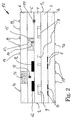
- FIG. 2 shows with the system 17 an alternative design of the system 1 after FIG. 1 , in which additionally on the outside of the support layer 6 and on the bottom of the rolling bearing 25 contacting bottom 1a further components 19 with thin-film technology are applied.
- Such components 19 are alternatively also applied to one of the layers 2, 3, 4 and 5 and thus enclosed by in each case two of the layers 2, 3, 4, 5 and 6.
- the components 19 are, for example, sensors and conductors, which can thus also be arranged directly between the surface of the roller bearing 25, on which the system 17 is fixed, and the carrier layer 2.
- FIG. 3 shows how the system 17 is installed in a rolling bearing ring 22 of the rolling bearing 25.
- the system is seated in a groove 23 of the rolling bearing ring 22 and is surrounded by the groove 23 on the underside 1a and on the flanks 1c.
- the top 1 b is optionally covered with a filling / protective layer, but not covered in this case.
- a compensation layer (modifier) 18 is applied for thermal expansion differences.
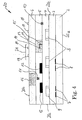
- the system 20 for data processing and data acquisition according to FIG. 4
- it is additionally provided with SMD components 21, for example ASICs.
- SMD components are unhoused contacted on the side remote from the surface of the rolling bearing top 20b on the support layer 6.
- the individual carrier layers 3, 4, 5, 6 are cast or injected in thick-film structure, wherein the individual structures of the components 7, 8, 9, 10, 11, 12, 14, 15, 16, 19, 21 are generated simultaneously. These layers 3, 4, 5, 6 are laminated together. As a result, the layers 2, 3, 4, 5, 6 are firmly bonded together, but the entire system is still soft and moldable. Only with the final sintering process takes the structure of the layers 2, 3, 4, 5, 6 then the predetermined outer contour (for example, the radius of curvature of an outer ring) in a corresponding shape, the later installation geometry of the rolling bearing ring and the housing of the rolling bearing 25th anticipates.
- the predetermined outer contour for example, the radius of curvature of an outer ring
- FIG. 5 shows how the system 20 is installed in a rolling bearing ring 22.
- To the system sits in a groove 23 of the rolling bearing ring 22 and is surrounded by the groove 23 on the underside 20a and on the flanks 20c.
- the groove 23 is filled above the system 20 with filler 24 which covers the top 20b of the system 20 and which partially encloses the components 19, 21.
- a compensation layer 18 is applied for thermal expansion differences.
- FIG. 6 a system 26 for data acquisition and data processing from the carrier layers 27, 28, 29, 30, a piezoelectric element 31, a liquid storage 32 and channels 33 and 34 is shown. Between the carrier layers 28 and 29, the channels 33 and 34 are formed and optionally interconnected. The channel 33 leads to the liquid reservoir 32, which is filled with a pressure fluid 35.
- the piezoelectric element 31 is optionally designed as an actuator, by means of which the pressure liquid 35 can be pressed into the channels 33, 34 by applying a voltage or is designed as a sensor, which by the pressure in the liquid reservoir 32 from the channels 33 and 34 into a voltage signal and thus measures the pressure.
Landscapes
- Chemical & Material Sciences (AREA)
- Analytical Chemistry (AREA)
- Physics & Mathematics (AREA)
- General Physics & Mathematics (AREA)
- Rolling Contact Bearings (AREA)
- Apparatus For Radiation Diagnosis (AREA)
Description
- Die Erfindung betrifft ein Wälzlager mit einem System zur Datenerfassung und zur Datenverarbeitung, wobei das System an dem Wälzlager fest ist und wenigstens ein Sensorelement zum Erfassen von physikalischen Größen, Leiterelemente und elektronische Bauelemente aufweist.
- Aus
DE 101 36 438 A1 ist ein Wälzlager bekannt, an dem zur Ermittlung physikalischer Größen Sensoren befestigt sind. Mit den Sensoren werden auf die Lagerringe des Wälzlagers wirkenden Kräfte und Momente, zum Beispiel elastische Verformungen aus Wälzkontakten, erfasst. Die Sensoren sind als Dehnmesswiderstände ausgebildet und vorzugsweise in einer Nut am Umfang eines der Lagerringe befestigt. Diese Dehnmesswiderstände sind über eine Isolationsschicht auf einem metallischen Zwischenträger aufgebracht. Ein weiteres Trägermaterial ist als Schaltungsträger ausgebildet und umgibt den metallischen Zwischenträger mit den Dehnmessstreifen. Der Schaltungsträger nimmt elektronische Bauteile und Leiterbahnen auf. Die Zwischenträgerschicht und die Schaltungsträgerschicht sind an dem Lagerring in die Nut eingepresst oder mit der Nut verschweißt. - In
DE 101 36 438 A1 sind als Voll- oder auch Halbbrückenschaltungen geschaltete Dehnmesswiderstände auf einem metallischen Zwischenträger beschrieben. Weiter nimmt das Wälzlager nachDE 101 36 438 A1 elektronische Bauelemente für die Auswertung der Sensorsignale und für die Übertragung dieser zu weiteren Messstellen oder zu einem Anschlussstecker bzw. zu einer Schaltung für die Auswertung der Signale auf. Die Übertragung der Signale in diesem Wälzlager wird dabei über Digital- oder Analogbussysteme, beispielsweise in einem Kraftfahrzeug, vorgenommen. - Die Nut zur Aufnahme des zuvor beschriebenen Systems zur Datenerfassung und Datenverarbeitung ist bei der Auslegung des Lagerringes und somit auch des Wälzlagers zu berücksichtigen. Ein Wälzlager ohne ein derartiges System ist nicht ohne weiteres gegen ein mit diesem System ausgestattetes bau- und größengleiches Lager austauschbar, da die Nut zur Aufnahme des Systems den entsprechenden Lagerring erheblich schwächen kann. Messlager in der Ausführung des Standes der Technik sind deshalb nicht in jedem Fall gegen größengleiche Lager ohne Messeinrichtung austauschbar, d. h. ein Wälzlager mit einem entsprechenden System ist in seinen Abmessungen in der Regel größer und kann deshalb nur nach Änderung der Umgebungskonstruktion in ein bestehendes System eingepasst werden.
- Aus der nicht vorveröffentlichten Anmeldung
DE 103 04 592 A1 sind Wälzlager mit dem beschriebenen System an flexiblen Folien bekannt. Dabei sind die einzelnen Bauelemente und deren Verbindungen auf die Folie aufgetragen und ggf. durch die Folie hindurch über Durchkontaktierungen miteinander verbunden. Derartige auf Folien beanspruchen zwar im Vergleich zu dem zuvor beschriebenen Stand der Technik weniger Bauraum sind aber jedoch relativ aufwendig herzustellen und an das Wälzlager zu montieren. Außerdem sind die Folien relativ empfindlich gegen mechanische Einflüsse und zum Beispiel gegen Schmierflüssigkeiten. -
WO 02/054031 A1 -
EP 1 148 261 A2 beschreibt ein Wälzlager mit einem System zur Erfassung von Kräften, wobei das System SAW- oder BAW-Sensoren umfasst, die in ringförmigen Nuten in dem Außenring des Wälzlagers angeordnet sind. Die SAW- bzw. BAW-Sensoren sind in unmittelbaren Kontakt mit dem Korpus des Außenrings angeordnet. Weil die SAW- bzw. BAW-Sensoren fest an dem Korpus des Außenrings angeordnet sind, ist eine Anpassung bei einer thermischen Ausdehnung des Außenrings 1 nicht möglich und auch nicht erforderlich. -
US 4,747,456 A beschreibt eine Kraftmessdose mit einem Zwischenteil aus einem metallischen Material mit einem deformierbaren Abschnitt, an dem ein dreilagiges System zum Erfassen von Kräften, speziell von Spannungen, vorgesehen ist. Auf das metallische Material ist eine Isolatorschicht z. B. aus SiO2 aufgebracht, auf diese wiederum eine erste Lage und eine zweite Lage. Die erste Lage ist aus einem hochohmigen Widerstandsmaterial wie NiCr und die dritte Lage aus einem elektrischen Leiter wie Kupfer hergestellt. Die Dehnmeßstreifen sind in der zweiten Lage ausgebildet und Teil eines elektrischen Meßsystems. Aufgrund der festen Verbindung der Isolierschicht mit dem metallischen Korpus des deformierbaren Abschnitts ist ein Ausgleich unterschiedlicher thermischer Dehnungen nicht möglich. -
DE 197 47 001 A1 beschreibt eine Welle mit einem Meßsystem zur Erfassung der Dehnung der Welle. Das Meßsystem umfasst eine dielektrische Schicht, die unmittelbar auf dem Korpus der Welle aufgebracht ist, eine Anordnung von einer Leiterbahn mit Kontaktflächen und einem Widerstand. Unmittelbar auf der Welle ist ein Dehnmeßstreifen angeordnet, der mit der Leiterbahn in Verbindung steht. Über der Leiterbahn ist eine Passivierungsschicht angeordnet. Die dielektrische Schicht umfasst beispielsweise eine Glasfritte, die über Oxidbrücken mit der Welle 1 fest verbunden ist. Die Druckschrift beschreibt keine Möglichkeit eines Ausgleichs thermischer induzierter Spannungen zwischen dem metallischen Material der Welle und der dielektrischen Schicht des Meßsystems. Die dielektrische Schicht ist mit dem Korpus der Welle fest verbunden. - Die Aufgabe der Erfindung ist es daher, ein Wälzlager mit einem System zur Datenerfassung und zur Datenverarbeitung zu schaffen, das sich kostengünstig herstellen lässt, wenig Bauraum beansprucht und gegen abmessungsgleiche Wälzlager ohne ein Messsystem austauschbar ist. Weiterhin ist ein Wälzlager mit einem derartigen System zu schaffen, das gegen Umwelteinflüsse wie Stoß und Erschütterungen, gegen Flüssigkeiten, insbesondere aggressive Mittel, relativ unempfindlich und das thermisch hoch widerstandsfähig ist.
- Diese Aufgabe ist nach dem Gegenstand des Anspruches 1 dadurch gelöst, dass das System zur Datenerfassung und zur Datenverarbeitung in einer Trägerschicht von stapelförmig aufeinander angeordneten und aneinander liegenden Trägerschichten aus mindestens einem keramischen Werkstoff ausgebildet ist und wobei zwei aufeinander liegende der Trägerschichten miteinander verbunden sind. Dabei sind die Bauelemente einzeln zumindest teilweise in einer der Trägerschichten aus Keramik eingebettet. Unter dem Begriff elektronische Bauelemente sind Elemente wie Sensoren, Leiterelemente, Widerstände, Kondensatoren und weitere für die Sensorik, Signalübertragung und Signalauswertung notwendigen Bauelemente zusammengefasst. Erfindungsgemäß ist eine an dem Wälzlager feste der Trägerschichten durch eine thermische Ausgleichsschicht von dem Wälzlager getrennt.
- Wahlweise sind die Trägerschichten Substrate für im Dickschichtverfahren oder Dünnschichtverfahren aufgetragene Bauelemente oder die Trägerschichten sind Träger von im SMD-Verfahren aufgebrachten Bauteilen. Alternativ dazu sind die Trägerschichten, die mit den Schaltungen versehenen sind im Dickschichtverfahren aufgetragene Schichten. Die Trägerschichten sind weiter Isolationsschichten und Basisschichten aus Keramik, die fundamentartig die anderen Trägeschichten des Systems aufnehmen oder abdecken und somit schützen. Diese Schichten der unterschiedlichsten Ausführung und mit den unterschiedlichen Funktionen sind lamellenartig in einem System aufeinander gestapelt. Dabei umfasst jede der Trägerschichten zum Beispiel einen Innenring oder einen Außenring des Wälzlagers - bzw. ist von diesem umfasst oder ist beispielsweise axial an einem der Lagerringe angeordnet. Die Erfindung ist an Linear- und Rotativlagern und dort wiederum an Gleit- und Wälzlagern einsetzbar.
- Mit der Dickschichttechnik werden im Siebdruckverfahren dünne Schichten aus Metalloxyden (Widerstände, Leiterbahnen) auf das Substrat oder eine weitere der Trägerschichten gedruckt. Die Schichtdicke derartiger Dickschichten ist vorzugsweise 1 - 80 Mikrometer. Die im Siedruckverfahren aufgetragenen Pasten sind feinkörnige Gemenge aus anorganischen Bestandteilen in einem organischen Trägermaterial, das weiterhin Metallpulver (Leitpasten), Metalloxyde (Widerstandspasten), Glasfritte oder Keramiken (Dieelektrika) enthält. Das Material wird mit dem Siebdruckverfahren auf die keramischen Substrate strukturiert aufgebracht und dann in einzelnen Schichten oder zusammen als Stapel eingebrannt.
- Alternativ werden mit der so genannten Dünnschichttechnik über Verdampfen von Metallen zur Bildung der Schaltkreise im Hochvakuum aufgetragen. Die Schichtdicke ist vorzugsweise 0,1 µm und wird jedoch beispielsweise mindestens noch auf 3 Mikrometer galvanisch verstärkt.
- Die Leiterbahnen sind auf Edelmetallbasis, zum Beispiel aus Palladium, Silber, Platin, Gold oder aus Legierungen von diesen gebildet. Die Isolationsschicht (Dieelektrikum für sich kreuzende Leiterbahnen) ist eine Glaskeramikschicht (Glas-Keramikpaste BaTiO3, TiO2, Mg, Zn oder CaTiO3). Weiter sind in die Keramikschichten Goldschicht-Pads für Bonddrähte und verschiedene Widerstandsschichten wie Schichten aus Palladiumoxyd/Silber, Iridiumoxyd/Platin- oder rutheniumhaltige Gemische vorgesehen.
- Außer den Dichtschicht bzw. Dünnschichtschaltungen sind SMD-Bauteite an der Oberfläche des Systems denkbar. SMD-Bauteile sind Surface-Mounted-Devices = auf Oberflächen montierte Bauteile, für die keine Bestückungslöcher in der entsprechenden Trägerschicht benötigt werden. Dazu wird zum Beispiel Lötpaste auf die Lötpads aufgetragen, die Bauteile werden anschließend zu den Kontakten und in der Paste positioniert und schließlich die Lötverbindung durch Schmelzen der Lötpaste hergestellt (Reflow-Lötverfahren). Ggf. werden die Verbindungen zwischen den Bauteilen durch Bonden hergestellt. Dabei sind die Bauteile mittels Drähten untereinander verbunden, wodurch auch Höhenunterschiede zwischen den Anschlüssen einzelner zu verbindender Elemente ausgeglichen werden können. Zum Beispiel ist bei Drahtbonden Bondmaterial aus AU oder AL-SI-Legierungen eingesetzt, das durch Thermokompressionsbonden bzw. Ultraschallbonden und Kugelkeilschweißverbindungen befestigt ist. Ggf. enthält das System auch Die-Bond-Bauteile. Unter Die-Bonden ist das Aufbringen kleiner Chips zu verstehen, die ungehäuste, d.h. unverpackte Halbleiter wie zum Beispiel Dioden und IC's, die mit Leit- oder nicht Leitkleber, durch Schweißen oder durch Löten befestigt sind. Diese Chips sind wahlweise mit den Goldbond-Pads über Aludraht oder Golddraht verdrahtet.
- Mittels einer Mehrlagendrucktechnik sind mehrere der Schaltungsebenen realisierbar. Dabei handelt es sich um eine Abfolge von innen nach außen oder von außen nach innen aufeinander gestapelter Leiterbahnen-, Isolator- und Widerstandsschichten. Löcher für die Durchkontaktierungen sind in der Regel in die Trägerschichten mit Laser eingebracht und mit Metall ausgefüllt.
- Für die Trägerschichten (Substrate) wird in der Regel Keramikpulver aus AL2O3 AIN- oder BeO-Keramik eingesetzt. Das Keramikpulver wird dazu mit verschiedenen Bindern fließfähig gemacht und in Formen gespritzt oder gegossen. Nach dem Befreien der Keramik von dem Binder werden die einzelnen Schichten ein oder beidseitig bestückt, mit oder ohne Durchkontaktierungen versehen aufeinander gestapelt und eingebrannt. Die Temperaturen für das Einbrennen liegen derzeit vorzugsweise in einem Bereich zwischen 500° - 900° C. Die einzelnen Trägerschichten weisen als Trägermaterial wahlweise unter einander den gleichen keramischen Werkstoff aber auch unterschiedliche keramische Werkstoffe auf.
- Die Vorteile des erfindungsgemäßen Systems zur Datenerfassung und zur Datenverarbeitung sind im wesentlichen:
- Platzersparnis und hohe Bauteildichte
- gute Wärmeableitung und Verteilung durch die Keramik, ggf. Kühlung durch gesonderte Kanäle in oder zwischen den Trägerschichten
- hohe Zuverlässigkeit durch wenig Lötverbindungen
- verbesserte elektrische Eigenschaften
- kürzere Schaltzeiten aufgrund der hohen Bauteildichte sowie kürzerer Verbindungen
- geringes Gewicht
- hohe mechanische Festigkeit gegen Stoß und Vibrationen
- widerstandsfähig gegen hohe Temperaturen
- hohe chemische Beständigkeit insbesondere gegen aggressive Medien
- die automatische Herstellung derartiger Systeme ist möglich
- Kostensenkung bei der Herstellung zum Beispiel durch Automatisierung.
- Durch die robuste Eigenschaft von Keramik gegen äußere chemische Einflüsse ist es möglich, Sensoren in der obersten Schicht bzw. in der untersten zum Lager hingewandten Schicht zu integrieren. Diese Sensoren sind beispielsweise Gassensoren aber auch die schon diskutierten Drucksensoren. Eine Ausgestaltung der Erfindung sieht deshalb das Aufbringen von Schichten oder Fasern aus Funktionskeramiken wie dieelektrische, piezokeramische oder auch magnetische Schichten, die bei Druck mit dem Aufbau einer elektrischen Ladung reagieren und die so die bekannten Widerstands-DMS ersetzen können.
- Die Systeme sind durch Kleben oder Einpressen in eine Nut auf der entsprechenden Oberfläche des Wälzlagers, zum Beispiel an einem Innenring, Außenring, einer Linearschiene eingebracht. Alternativ sind die Systeme als ein Gehäuse o.ä. ein Bestandteil des Lagers. Die Lagerteile, auf denen die Systeme befestigt sind, sind wahlweise aus Stahl oder aus Keramik aber auch aus allen anderen denkbaren Werkstoffen hergestellt.
- Die Erfindung wird nachfolgend anhand von Ausführungsbeispielen näher erläutert. Es zeigen im Einzelnen:
- Figur 1
- Die schematische Darstellung eines Systems zur Datenerfassung und zur Datenverarbeitung, das auf ein nicht weiter dargestelltes Wälzlager aufgebracht ist und bei dem die einzelnen Schichten in Dickschichttechnik aufgebracht und miteinander laminiert sind - die Darstellung im Schnitt,
- Figur 2
- das System nach
Figur 1 , an dem jedoch zusätzlich mit Dünnschichttechnik aufgebrachte Strukturen ausgebildet sind, - Figur 3
- das System nach
Figur 2 in einem Wälzlagerring - Figur 4
- das System nach
Figur 2 , an dem zusätzlich SMD-Bauelemente angeordnet sind, - Figur 5
- das System nach
Figur 3 in einem Wälzlagerring, - Figur 6
- den Ausschnitt eines erfindungsgemäßen Systems, mit einem Druck aktivierenden/aktiviertem Piezoelement,
-
Figur 1 zeigt ein System 1 zur Datenerfassung und zur Datenverarbeitung an einem nicht dargestellten Wälzlager mit den Trägerschichten 2, 3, 4, 5, 6. Das System ist stark vergrößert und nicht maßstäblich dargestellt. Die Unterseite 1a des Systems 1 liegt zum Beispiel an der Oberfläche eines Wälzlagers 25 zum Erfassen von Verformungen an dieser Oberfläche an. Das System 1 ist wahlweise wie das System 17 (Figur 3 ) in eine Nut 23 eines Wälzlagerringes 22 eines Wälzlagers 25 eingebracht, wobei das System 1 zumindest teilweise an der Unterseite 1a und an den Flanken 1 c von der Nut 23 umgriffen ist. Alternativ dazu ist das System 1 an den Flanken 1c und an der Oberseite von einem Gehäuse beispielsweise aus Keramik oder einem Kunstharz bzw. aus anderen geeigneten Werkstoffen umgeben und sitzt mit der Unterseite 1a auf einer ebenen Oberfläche eines Wälzlagers ohne Nut. - Die Trägerschicht 2 ist eine Schicht aus Keramik an der sich das System zum Wälzlagerring abstützt. Die Trägerschicht 3 ist ein Substrat, dass in Mäanderform ausgebildete Leiterbahnen 7 und DMS 8 aufnimmt. Das Substrat ist aus Keramik. Die Trägerschicht 4 ist eine im Dickschichtverfahren aufgetragene keramische Schicht mit passiven elektrischen Bauelementen 9, wie Kondensatoren und Widerständen.
- Radial zwischen der Trägerschicht 4 und der Trägerschicht 5 ist ein Kanal 10 ausgebildet, der beispielsweise mit dem Kanal 11 in der Trägerschicht 5 verbunden ist. Die Kanäle 10 und 11 sind wahlweise mit einer technischen Flüssigkeit gefüllt.
- Die Trägerschicht 5 ist eine im Dickschichtverfahren aufgetragene keramische Schicht mit elektrischen Leiterbahnen 12, einem Sensor 13, beispielsweise einem Beschleunigungssensor, wobei in der Umgebung des Sensors ein Hohlraum 14 und die seismische Masse mit Kontaktierung 15 ausgebildet sind. Die Trägerschicht 6 schließt das System 1 radial nach außen ab und ist mit mindestens einem Sensor 16 als Druck-/Gassensor versehen. Der Gassensor ist seitens der Oberseite 1 b radial von außen zugängig.
-
Figur 2 zeigt mit dem System 17 eine alternative Gestaltung des Systems 1 nachFigur 1 , bei dem zusätzlich außen auf die Trägerschicht 6 und an der das Wälzlager 25 berührenden Unterseite 1a weitere Bauelemente 19 mit Dünnschichttechnik aufgebracht sind. Derartige Bauelemente 19 sind alternativ auch auf eine der Schichten 2, 3, 4 und 5 aufgetragen und somit von jeweils zwei der Schichten 2, 3, 4, 5 und 6 eingeschlossen. Die Bauelemente 19 sind zum Beispiel Sensoren und Leiter, die somit auch direkt zwischen der Oberfläche des Wälzlagers 25, an dem das System 17 fest ist, und der Trägerschicht 2 angeordnet sein können. -
Figur 3 zeigt, wie das System 17 in einem Wälzlagerring 22 des Wälzlagers 25 verbaut ist. Dazu sitzt das System in einer Nut 23 des Wälzlagerringes 22 und ist an der Unterseite 1a und an den Flanken 1c von der Nut 23 umgeben. Die Oberseite 1 b ist wahlweise mit einer Füll-/Schutzschicht abgedeckt, in diesem Fall aber nicht abgedeckt. Zwischen dem System 17 und dem Wälzlager 25 ist eine Ausgleichsschicht (Modifizierer) 18 für thermische Dehnungsdifferenzen aufgetragen. - Das System 20 zur Datenverarbeitung und zur Datenerfassung nach
Figur 4 ist alternativ zu dem System 1 zusätzlich mit SMD-Bauelementen 21, zum Beispiel ASIC's versehen. Die SMD-Bauelemente sind ungehäust auf der von der Oberfläche des Wälzlagers abgewandten Oberseite 20b auf die Trägerschicht 6 kontaktiert. - Die einzelnen Trägerschichten 3, 4, 5, 6 sind in Dickschichtstruktur gegossen oder gespritzt, wobei die einzelnen Strukturen der Bauelemente 7, 8, 9, 10, 11, 12, 14, 15, 16, 19, 21 gleichzeitig erzeugt werden. Diese Schichten 3, 4, 5, 6 werden miteinander laminiert. Als Ergebnis sind die Schichten 2, 3, 4, 5, 6 fest miteinander verbunden, jedoch ist das gesamte System weiterhin weich und formbar. Erst mit dem abschließenden Sinterprozess nimmt die Struktur aus den Schichten 2, 3, 4, 5, 6 dann die vorgegebene äußere Kontur (zum Beispiel den Krümmungsradius eines Außenringes) in einer entsprechenden Form, die die spätere Einbaugeometrie des Wälzlagerringes und des Gehäuses des Wälzlagers 25 vorwegnimmt, an.
-
Figur 5 zeigt, wie das System 20 in einem Wälzlagerring 22 verbaut ist. Dazu sitzt das System in einer Nut 23 des Wälzlagerringes 22 und ist an der Unterseite 20a und an den Flanken 20c von der Nut 23 umgeben. Die Nut 23 ist oberhalb des Systems 20 mit Füllmaterial 24 aufgefüllt, das die Oberseite 20b des Systems 20 abdeckt und das die Bauelemente19, 21 teilweise einschließt. Zwischen dem System 20 und dem Wälzlager 25 ist eine Ausgleichsschicht 18 für thermische Dehnungsdifferenzen aufgetragen. - In
Figur 6 ist ein System 26 zur Datenerfassung und zur Datenverarbeitung aus den Trägerschichten 27, 28, 29, 30, aus einem Piezoelement 31, einem Flüssigkeitsspeicher 32 und Kanälen 33 und 34 dargestellt. Zwischen den Trägerschichten 28 und 29 sind die Kanäle 33 und 34 ausgebildet und wahlweise miteinander verbunden. Der Kanal 33 führt zu dem Flüssigkeitsspeicher 32, der mit einer Druckflüssigkeit 35 gefüllt ist. Das Piezoelement 31 ist wahlweise als Aktuator ausgebildet, mit dem durch Anlegen einer Spannung die DruckFlüssigkeit 35 in die Kanäle 33, 34 gedrückt werden kann oder ist als Sensor ausgelegt, der durch den Druck in dem Flüssigkeitsspeicher 32 aus den Kanälen 33 und 34 in ein Spannungssignal umsetzt und somit den Druck misst. -
- 1
- System
- 1a
- Unterseite
- 1 b
- Oberseite
- 1c
- Flanken
- 2
- Trägerschicht
- 3
- Trägerschicht
- 4
- Trägerschicht
- 5
- Trägerschicht
- 6
- Trägerschicht
- 7
- Leiterbahnen
- 8
- DMS
- 9
- Passive Bauelemente
- 10
- Kanal
- 11
- Kanal
- 12
- Leiterbahnen
- 13
- Sensor
- 14
- Hohlraum
- 15
- Kontaktierung
- 16
- Sensor
- 17
- System
- 18
- Ausgleichsschicht
- 19
- Bauelement
- 20
- System
- 20a
- Unterseite
- 20b
- Oberseite
- 20c
- Flanken
- 21
- SMD-Bauelemente
- 22
- Wälzlagerring
- 23
- Nut
- 24
- Füllmaterial
- 25
- Wälzlager
- 26
- System
- 27
- Trägerschichten
- 28
- Trägerschichten
- 29
- Trägerschichten
- 30
- Trägerschichten
- 31
- Piezoelement
- 32
- Flüssigkeitsspeicher
- 33
- Kanal
- 34
- Kanal
- 35
- Druckflüssigkeit
Claims (13)
- Wälzlager (25) mit einem System (1, 18, 20, 26) zur Datenerfassung und zur Datenverarbeitung, wobei das System (1, 18, 20, 26) an dem Wälzlager (25) fest Ist und wenigstens ein Sensorelement (8, 13, 16, 31) zum Erfassen von physikalischen Größen, Leiterelemente (7, 12, 15) und elektronische Bauelemente (9, 19, 21) aufweist, und wobei wenigstens ein erstes Element (7, 8, 9, 12, 13, 14, 15, 16) der Elemente (7, 8, 9, 12, 13, 14, 15, 16, 19, 21) In eine Trägerschicht (3, 4, 5, 6, 28, 29, 30) von stapelförmig aufeinander angeordneten und aneinander liegenden Trägerschichten (2, 3, 4, 5, 6, 27, 28, 29, 30) zumindest teilweise eingebettet ist, wobei die Trägerschichten (2, 3, 4, 5, 6, 27, 28, 29, 30) aus mindestens einem keramischen Werkstoff bestehen sowie jeweils zwei aufeinander liegende der Trägerschichten (2, 3, 4, 6, 6, 27, 28, 29, 30) miteinander verbunden sind, und bei dem eine an dem Wälzlager (25) feste der Trägerschichten (2, 3, 4, 5, 6, 27, 28, 29, 30) durch eine thermische Ausgleichschicht (18) von dem Wälzlager (25) getrennt ist.
- Wälzlager (25) nach Anspruch 1, bei dem wenigsten eine der Trägerschichten (3, 4, 5, 6) ein Substrat für im Dickschichtverfahren aufgetragene Elemente ist.
- Wälzlager (25) nach Anspruch 1, bei dem wenigstens drei der Trägerschichten (2, 3, 4, 5, 6, 27, 28, 29, 30) eine Abfolge aufeinander gestapelter Leiterbahnen-, Wlderstands- und Isolationsschichten sind.
- Wälzlager nach Anspruch 1, bei dem wenigstens eine der Trägerschichten (2, 6) Im Dünnschltverfahren aufgetragene erste Elemente (19) der Elemente (7, 8, 9, 12, 13, 14, 15, 16, 19, 21) trägt.
- Wälzlager (25) nach Anspruch 1, bei dem zumindest ein zweites Element (7, 8, 9, 12, 13, 14, 15, 16) der Elemente (7, 8, 9, 12, 13, 14, 15, 16, 19, 21) von zwei der Trägerschichten (2, 3, 4, 5, 6, 27, 28, 29, 30) eingeschiossenist.
- Wälzlager (25) nach Anspruch 5, bei der wenigstens ein drittes Element (7, 8, 9, 12, 13, 15, 16) der zweiten Elemente (7, 8, 9, 12, 13, 14, 15, 16) an einer Außenfläche einer ersten Trägerschicht (2, 3, 4, 5) zumindest anliegt, wobei die erste Trägerschicht (2, 3, 4, 5) zwischen einer zweiten Trägerschicht (3, 4, 5, 6) und einer Oberfläche des Wälzlagers (25) angeordnet ist und wobei das System (1,17, 20) zumindest an der Oberfläche fest ist.
- Wälzlager (25) nach Anspruch 5, bei dem zumindest ein viertes Element (13) der ersten Elemente (7, 8, 9, 12, 13, 14, 15, 16) mit einer von einer Oberfläche an dem Wälzlager (25) wegweisenden Außenfläche an einer fünften Trägerschicht (6) der Trägerschichten (2, 3, 4, 5, 6, 27, 28, 29, 30) anliegt, wobei das vierte Element (13) zwischen der fünften Trägerschicht (6) und einer Oberfläche des Wälzlagers 25 angeordnet ist und wobei das System (1, 17, 20) zumindest an der Oberfläche fest ist.
- Wälzlager (25) nach Anspruch 1 bei dem wenigstens eine der TrägerSchichten (2, 3, 4, 5, 6, 27, 28, 29, 30) das Wälzlager (25) umfangsseitig vollständig umgreift.
- Wälzlager (25) nach Anspruch 1, bei dem wenigstens ein Element (19, 21) der Elemente (7, 8, 9, 12, 13, 14, 15, 16, 19, 21) ein auf eine Trägerschicht (6) der Trägerschichten (2, 3, 4, 5, 8, 27, 28, 29, 30) oberflächenmontiertes Bauelement (SMD) ist.
- Wälzlager (25) nach Anspruch 1, bei dem das Sensorelement (8, 13, 16, 31) wenigstens eine plezokeramlsche Schicht Ist.
- Wälzlager (25) nach Anspruch 1, bei dem das Sensorelement (8, 13, 16, 31) zumindest eine piezokeramische Faser ist.
- Wälzlager (25) nach Anspruch 1, bei dem das Sensorelement (8, 13, 16, 31) wenigstens ein Dehnmessstreifen ist.
- Wälzlager (25) nach einem der Ansprüche 1 bis 12, wobei die einzelnen Trägerschichten (3, 4, 5, 6) In Dlckschichtstruktur gegossen oder gespritzt sind, und wobei die einzelnen Strukturen der Bauelemente (7, 8, 9, 10, 11, 12, 14, 15, 16, 19, 21) gleichzeitig erzeugt worden sind, und wonach die Trägerschichten (3, 4, 5, 6) miteinander laminiert worden sind.
Applications Claiming Priority (2)
| Application Number | Priority Date | Filing Date | Title |
|---|---|---|---|
| DE10355817A DE10355817A1 (de) | 2003-11-28 | 2003-11-28 | Wälzlager mit einem System zur Datenerfassung und zur Datenverarbeitung |
| PCT/DE2004/002606 WO2005052395A1 (de) | 2003-11-28 | 2004-11-24 | Wälzlager mit einem system zur datenerfassung und zur datenverarbeitung |
Publications (2)
| Publication Number | Publication Date |
|---|---|
| EP1716341A1 EP1716341A1 (de) | 2006-11-02 |
| EP1716341B1 true EP1716341B1 (de) | 2009-12-30 |
Family
ID=34625382
Family Applications (1)
| Application Number | Title | Priority Date | Filing Date |
|---|---|---|---|
| EP04802815A Expired - Lifetime EP1716341B1 (de) | 2003-11-28 | 2004-11-24 | Wälzlager mit einem system zur datenerfassung und zur datenverarbeitung |
Country Status (4)
| Country | Link |
|---|---|
| EP (1) | EP1716341B1 (de) |
| AT (1) | ATE453809T1 (de) |
| DE (2) | DE10355817A1 (de) |
| WO (1) | WO2005052395A1 (de) |
Cited By (1)
| Publication number | Priority date | Publication date | Assignee | Title |
|---|---|---|---|---|
| DE102020120113A1 (de) | 2020-07-30 | 2021-07-22 | Schaeffler Technologies AG & Co. KG | Präzisionsbauteil und Verfahren zur Aufbringung eines Sensorelements auf ein Präzisionsbauteil |
Families Citing this family (2)
| Publication number | Priority date | Publication date | Assignee | Title |
|---|---|---|---|---|
| DE102008034654A1 (de) * | 2008-07-25 | 2010-02-04 | Knorr-Bremse Systeme für Nutzfahrzeuge GmbH | Sensoreinrichtung |
| DE102015100655A1 (de) * | 2015-01-19 | 2016-07-21 | Cord Winkelmann | Linearführungseinrichtung für eine Vorschubachse einer Werkzeugmaschine |
Family Cites Families (5)
| Publication number | Priority date | Publication date | Assignee | Title |
|---|---|---|---|---|
| JPS62226029A (ja) * | 1986-03-28 | 1987-10-05 | Tokyo Electric Co Ltd | ロ−ドセルの温度補正方法 |
| DE4218949A1 (de) * | 1992-06-10 | 1993-12-16 | Schaeffler Waelzlager Kg | Kraftmeßlager |
| DE19747001C2 (de) * | 1997-10-24 | 2000-02-24 | Mannesmann Vdo Ag | Dehnungsmeßstreifen sowie ein mit diesen Dehnungsmeßstreifen hergestellter mechanisch-elektrischer Wandler |
| DE19954164B4 (de) * | 1999-11-10 | 2008-08-21 | Fraunhofer-Gesellschaft zur Förderung der angewandten Forschung e.V. | Sensor zur Zustandsbestimmung von Kenngrößen an mechanischen Komponenten unter Verwendung von amorphen Kohlenstoffschichten mit piezoresistiven Eigenschaften |
| DE10017572B4 (de) * | 2000-04-10 | 2008-04-17 | INSTITUT FüR MIKROTECHNIK MAINZ GMBH | Wälzlager mit fernabfragbaren Erfassungseinheiten |
-
2003
- 2003-11-28 DE DE10355817A patent/DE10355817A1/de not_active Withdrawn
-
2004
- 2004-11-24 AT AT04802815T patent/ATE453809T1/de not_active IP Right Cessation
- 2004-11-24 WO PCT/DE2004/002606 patent/WO2005052395A1/de not_active Ceased
- 2004-11-24 EP EP04802815A patent/EP1716341B1/de not_active Expired - Lifetime
- 2004-11-24 DE DE502004010605T patent/DE502004010605D1/de not_active Expired - Lifetime
Cited By (1)
| Publication number | Priority date | Publication date | Assignee | Title |
|---|---|---|---|---|
| DE102020120113A1 (de) | 2020-07-30 | 2021-07-22 | Schaeffler Technologies AG & Co. KG | Präzisionsbauteil und Verfahren zur Aufbringung eines Sensorelements auf ein Präzisionsbauteil |
Also Published As
| Publication number | Publication date |
|---|---|
| EP1716341A1 (de) | 2006-11-02 |
| DE502004010605D1 (de) | 2010-02-11 |
| DE10355817A1 (de) | 2005-07-21 |
| ATE453809T1 (de) | 2010-01-15 |
| WO2005052395A1 (de) | 2005-06-09 |
Similar Documents
| Publication | Publication Date | Title |
|---|---|---|
| EP2107604B1 (de) | Leistungshalbleitermodul mit hermetisch dichter Schaltungsanordnung und Herstellungsverfahren hierzu | |
| DE102004026246A1 (de) | Rollkörper | |
| DE102013101731A1 (de) | Drucksensorsystem | |
| DE102009060002A1 (de) | Sensor | |
| WO2000011376A2 (de) | Steuergerät in einem kraftfahrzeug | |
| EP3931540B1 (de) | Messgerät mit einem sensorelement und einer mess- und betriebsschaltung | |
| DE102016101246A1 (de) | Sensoranordnung und Verfahren zur Herstellung einer Sensoranordnung | |
| US8193898B2 (en) | Laminated body and manufacturing method thereof | |
| DE19747001C2 (de) | Dehnungsmeßstreifen sowie ein mit diesen Dehnungsmeßstreifen hergestellter mechanisch-elektrischer Wandler | |
| DE102008054879B4 (de) | Drucksensor | |
| DE102007026827A1 (de) | Aufnehmer zur Messung mechanischer Kräfte und Momente | |
| EP1794559B1 (de) | Sensorvorrichtung | |
| DE10355817A1 (de) | Wälzlager mit einem System zur Datenerfassung und zur Datenverarbeitung | |
| EP1204301B1 (de) | Aufbau zur Bildung einer Eingangsschaltung zur Aufnahme und Verarbeitung eines elektrischen Signals | |
| WO2010079004A1 (de) | Sensoranordnung und verfahren zur herstellung einer sensoranordnung | |
| WO2006084767A1 (de) | Piezoelektrischer sensor mit thermosensor und verstärkerschaltung | |
| DE3818191C2 (de) | ||
| WO1997022865A1 (de) | Kraftmessvorrichtung | |
| DE10055943A1 (de) | Vorrichtung zur Messung eines Belastungszustandes | |
| WO2021032878A1 (de) | Sensorbauteil, halbzeug, verfahren zur anbringung und zur herstellung eines sensorbauteils | |
| US10842030B2 (en) | Method for through-plating a printed circuit board and such a printed circuit board | |
| DE10156160B4 (de) | Mechanisch-elektrischer Wandler | |
| DE102024207843A1 (de) | Sensorwälzkörper und Verfahren zum Herstellen eines Sensorwälzkörpers | |
| DE29724622U1 (de) | Elektronisches Bauelement | |
| DE102020126878A1 (de) | Druckmesszelle und Verfahren zur Herstellung einer Druckmesszelle |
Legal Events
| Date | Code | Title | Description |
|---|---|---|---|
| PUAI | Public reference made under article 153(3) epc to a published international application that has entered the european phase |
Free format text: ORIGINAL CODE: 0009012 |
|
| 17P | Request for examination filed |
Effective date: 20060526 |
|
| AK | Designated contracting states |
Kind code of ref document: A1 Designated state(s): AT BE BG CH CY CZ DE DK EE ES FI FR GB GR HU IE IS IT LI LU MC NL PL PT RO SE SI SK TR |
|
| DAX | Request for extension of the european patent (deleted) | ||
| 17Q | First examination report despatched |
Effective date: 20080303 |
|
| GRAP | Despatch of communication of intention to grant a patent |
Free format text: ORIGINAL CODE: EPIDOSNIGR1 |
|
| GRAS | Grant fee paid |
Free format text: ORIGINAL CODE: EPIDOSNIGR3 |
|
| GRAA | (expected) grant |
Free format text: ORIGINAL CODE: 0009210 |
|
| AK | Designated contracting states |
Kind code of ref document: B1 Designated state(s): AT BE BG CH CY CZ DE DK EE ES FI FR GB GR HU IE IS IT LI LU MC NL PL PT RO SE SI SK TR |
|
| REG | Reference to a national code |
Ref country code: GB Ref legal event code: FG4D Free format text: NOT ENGLISH |
|
| REG | Reference to a national code |
Ref country code: CH Ref legal event code: EP |
|
| REG | Reference to a national code |
Ref country code: IE Ref legal event code: FG4D |
|
| REF | Corresponds to: |
Ref document number: 502004010605 Country of ref document: DE Date of ref document: 20100211 Kind code of ref document: P |
|
| REG | Reference to a national code |
Ref country code: SE Ref legal event code: TRGR |
|
| PG25 | Lapsed in a contracting state [announced via postgrant information from national office to epo] |
Ref country code: FI Free format text: LAPSE BECAUSE OF FAILURE TO SUBMIT A TRANSLATION OF THE DESCRIPTION OR TO PAY THE FEE WITHIN THE PRESCRIBED TIME-LIMIT Effective date: 20091230 |
|
| REG | Reference to a national code |
Ref country code: NL Ref legal event code: VDEP Effective date: 20091230 |
|
| RAP2 | Party data changed (patent owner data changed or rights of a patent transferred) |
Owner name: SCHAEFFLER TECHNOLOGIES GMBH & CO. KG |
|
| PG25 | Lapsed in a contracting state [announced via postgrant information from national office to epo] |
Ref country code: PL Free format text: LAPSE BECAUSE OF FAILURE TO SUBMIT A TRANSLATION OF THE DESCRIPTION OR TO PAY THE FEE WITHIN THE PRESCRIBED TIME-LIMIT Effective date: 20091230 Ref country code: SI Free format text: LAPSE BECAUSE OF FAILURE TO SUBMIT A TRANSLATION OF THE DESCRIPTION OR TO PAY THE FEE WITHIN THE PRESCRIBED TIME-LIMIT Effective date: 20091230 |
|
| REG | Reference to a national code |
Ref country code: IE Ref legal event code: FD4D |
|
| PG25 | Lapsed in a contracting state [announced via postgrant information from national office to epo] |
Ref country code: PT Free format text: LAPSE BECAUSE OF FAILURE TO SUBMIT A TRANSLATION OF THE DESCRIPTION OR TO PAY THE FEE WITHIN THE PRESCRIBED TIME-LIMIT Effective date: 20100430 Ref country code: IS Free format text: LAPSE BECAUSE OF FAILURE TO SUBMIT A TRANSLATION OF THE DESCRIPTION OR TO PAY THE FEE WITHIN THE PRESCRIBED TIME-LIMIT Effective date: 20100430 Ref country code: RO Free format text: LAPSE BECAUSE OF FAILURE TO SUBMIT A TRANSLATION OF THE DESCRIPTION OR TO PAY THE FEE WITHIN THE PRESCRIBED TIME-LIMIT Effective date: 20091230 Ref country code: EE Free format text: LAPSE BECAUSE OF FAILURE TO SUBMIT A TRANSLATION OF THE DESCRIPTION OR TO PAY THE FEE WITHIN THE PRESCRIBED TIME-LIMIT Effective date: 20091230 Ref country code: ES Free format text: LAPSE BECAUSE OF FAILURE TO SUBMIT A TRANSLATION OF THE DESCRIPTION OR TO PAY THE FEE WITHIN THE PRESCRIBED TIME-LIMIT Effective date: 20100410 Ref country code: NL Free format text: LAPSE BECAUSE OF FAILURE TO SUBMIT A TRANSLATION OF THE DESCRIPTION OR TO PAY THE FEE WITHIN THE PRESCRIBED TIME-LIMIT Effective date: 20091230 Ref country code: BG Free format text: LAPSE BECAUSE OF FAILURE TO SUBMIT A TRANSLATION OF THE DESCRIPTION OR TO PAY THE FEE WITHIN THE PRESCRIBED TIME-LIMIT Effective date: 20100330 |
|
| PG25 | Lapsed in a contracting state [announced via postgrant information from national office to epo] |
Ref country code: SK Free format text: LAPSE BECAUSE OF FAILURE TO SUBMIT A TRANSLATION OF THE DESCRIPTION OR TO PAY THE FEE WITHIN THE PRESCRIBED TIME-LIMIT Effective date: 20091230 Ref country code: CZ Free format text: LAPSE BECAUSE OF FAILURE TO SUBMIT A TRANSLATION OF THE DESCRIPTION OR TO PAY THE FEE WITHIN THE PRESCRIBED TIME-LIMIT Effective date: 20091230 |
|
| PG25 | Lapsed in a contracting state [announced via postgrant information from national office to epo] |
Ref country code: IE Free format text: LAPSE BECAUSE OF FAILURE TO SUBMIT A TRANSLATION OF THE DESCRIPTION OR TO PAY THE FEE WITHIN THE PRESCRIBED TIME-LIMIT Effective date: 20091230 Ref country code: CY Free format text: LAPSE BECAUSE OF FAILURE TO SUBMIT A TRANSLATION OF THE DESCRIPTION OR TO PAY THE FEE WITHIN THE PRESCRIBED TIME-LIMIT Effective date: 20091230 Ref country code: GR Free format text: LAPSE BECAUSE OF FAILURE TO SUBMIT A TRANSLATION OF THE DESCRIPTION OR TO PAY THE FEE WITHIN THE PRESCRIBED TIME-LIMIT Effective date: 20100331 |
|
| PLBE | No opposition filed within time limit |
Free format text: ORIGINAL CODE: 0009261 |
|
| STAA | Information on the status of an ep patent application or granted ep patent |
Free format text: STATUS: NO OPPOSITION FILED WITHIN TIME LIMIT |
|
| 26N | No opposition filed |
Effective date: 20101001 |
|
| PG25 | Lapsed in a contracting state [announced via postgrant information from national office to epo] |
Ref country code: DK Free format text: LAPSE BECAUSE OF FAILURE TO SUBMIT A TRANSLATION OF THE DESCRIPTION OR TO PAY THE FEE WITHIN THE PRESCRIBED TIME-LIMIT Effective date: 20091230 |
|
| PGFP | Annual fee paid to national office [announced via postgrant information from national office to epo] |
Ref country code: IT Payment date: 20101127 Year of fee payment: 7 Ref country code: GB Payment date: 20101130 Year of fee payment: 7 |
|
| REG | Reference to a national code |
Ref country code: GB Ref legal event code: 732E Free format text: REGISTERED BETWEEN 20110407 AND 20110413 |
|
| BERE | Be: lapsed |
Owner name: SCHAEFFLER K.G. Effective date: 20101130 |
|
| PG25 | Lapsed in a contracting state [announced via postgrant information from national office to epo] |
Ref country code: MC Free format text: LAPSE BECAUSE OF NON-PAYMENT OF DUE FEES Effective date: 20101130 |
|
| REG | Reference to a national code |
Ref country code: CH Ref legal event code: PL |
|
| PG25 | Lapsed in a contracting state [announced via postgrant information from national office to epo] |
Ref country code: LI Free format text: LAPSE BECAUSE OF NON-PAYMENT OF DUE FEES Effective date: 20101130 Ref country code: CH Free format text: LAPSE BECAUSE OF NON-PAYMENT OF DUE FEES Effective date: 20101130 |
|
| PG25 | Lapsed in a contracting state [announced via postgrant information from national office to epo] |
Ref country code: BE Free format text: LAPSE BECAUSE OF NON-PAYMENT OF DUE FEES Effective date: 20101130 |
|
| PGFP | Annual fee paid to national office [announced via postgrant information from national office to epo] |
Ref country code: FR Payment date: 20111214 Year of fee payment: 8 Ref country code: SE Payment date: 20111130 Year of fee payment: 8 |
|
| REG | Reference to a national code |
Ref country code: AT Ref legal event code: MM01 Ref document number: 453809 Country of ref document: AT Kind code of ref document: T Effective date: 20101124 |
|
| PG25 | Lapsed in a contracting state [announced via postgrant information from national office to epo] |
Ref country code: AT Free format text: LAPSE BECAUSE OF NON-PAYMENT OF DUE FEES Effective date: 20101124 |
|
| PG25 | Lapsed in a contracting state [announced via postgrant information from national office to epo] |
Ref country code: LU Free format text: LAPSE BECAUSE OF NON-PAYMENT OF DUE FEES Effective date: 20101124 Ref country code: HU Free format text: LAPSE BECAUSE OF FAILURE TO SUBMIT A TRANSLATION OF THE DESCRIPTION OR TO PAY THE FEE WITHIN THE PRESCRIBED TIME-LIMIT Effective date: 20100701 |
|
| REG | Reference to a national code |
Ref country code: DE Ref legal event code: R081 Ref document number: 502004010605 Country of ref document: DE Owner name: SCHAEFFLER TECHNOLOGIES AG & CO. KG, DE Free format text: FORMER OWNER: SCHAEFFLER TECHNOLOGIES GMBH & CO. KG, 91074 HERZOGENAURACH, DE Effective date: 20120828 Ref country code: DE Ref legal event code: R081 Ref document number: 502004010605 Country of ref document: DE Owner name: SCHAEFFLER TECHNOLOGIES GMBH & CO. KG, DE Free format text: FORMER OWNER: SCHAEFFLER TECHNOLOGIES GMBH & CO. KG, 91074 HERZOGENAURACH, DE Effective date: 20120828 |
|
| PG25 | Lapsed in a contracting state [announced via postgrant information from national office to epo] |
Ref country code: TR Free format text: LAPSE BECAUSE OF FAILURE TO SUBMIT A TRANSLATION OF THE DESCRIPTION OR TO PAY THE FEE WITHIN THE PRESCRIBED TIME-LIMIT Effective date: 20091230 |
|
| GBPC | Gb: european patent ceased through non-payment of renewal fee |
Effective date: 20121124 |
|
| PG25 | Lapsed in a contracting state [announced via postgrant information from national office to epo] |
Ref country code: SE Free format text: LAPSE BECAUSE OF NON-PAYMENT OF DUE FEES Effective date: 20121125 |
|
| REG | Reference to a national code |
Ref country code: FR Ref legal event code: ST Effective date: 20130731 |
|
| PG25 | Lapsed in a contracting state [announced via postgrant information from national office to epo] |
Ref country code: IT Free format text: LAPSE BECAUSE OF NON-PAYMENT OF DUE FEES Effective date: 20121124 |
|
| PG25 | Lapsed in a contracting state [announced via postgrant information from national office to epo] |
Ref country code: FR Free format text: LAPSE BECAUSE OF NON-PAYMENT OF DUE FEES Effective date: 20121130 Ref country code: GB Free format text: LAPSE BECAUSE OF NON-PAYMENT OF DUE FEES Effective date: 20121124 |
|
| REG | Reference to a national code |
Ref country code: DE Ref legal event code: R081 Ref document number: 502004010605 Country of ref document: DE Owner name: SCHAEFFLER TECHNOLOGIES AG & CO. KG, DE Free format text: FORMER OWNER: SCHAEFFLER TECHNOLOGIES AG & CO. KG, 91074 HERZOGENAURACH, DE Effective date: 20140213 Ref country code: DE Ref legal event code: R081 Ref document number: 502004010605 Country of ref document: DE Owner name: SCHAEFFLER TECHNOLOGIES GMBH & CO. KG, DE Free format text: FORMER OWNER: SCHAEFFLER TECHNOLOGIES AG & CO. KG, 91074 HERZOGENAURACH, DE Effective date: 20140213 |
|
| PGFP | Annual fee paid to national office [announced via postgrant information from national office to epo] |
Ref country code: DE Payment date: 20140131 Year of fee payment: 10 |
|
| REG | Reference to a national code |
Ref country code: DE Ref legal event code: R081 Ref document number: 502004010605 Country of ref document: DE Owner name: SCHAEFFLER TECHNOLOGIES AG & CO. KG, DE Free format text: FORMER OWNER: SCHAEFFLER TECHNOLOGIES GMBH & CO. KG, 91074 HERZOGENAURACH, DE Effective date: 20150126 |
|
| REG | Reference to a national code |
Ref country code: DE Ref legal event code: R119 Ref document number: 502004010605 Country of ref document: DE |
|
| PG25 | Lapsed in a contracting state [announced via postgrant information from national office to epo] |
Ref country code: DE Free format text: LAPSE BECAUSE OF NON-PAYMENT OF DUE FEES Effective date: 20150602 |
|
| P01 | Opt-out of the competence of the unified patent court (upc) registered |
Effective date: 20230523 |