EP1713645B1 - Grid image with several grid fields - Google Patents
Grid image with several grid fields Download PDFInfo
- Publication number
- EP1713645B1 EP1713645B1 EP05701144.7A EP05701144A EP1713645B1 EP 1713645 B1 EP1713645 B1 EP 1713645B1 EP 05701144 A EP05701144 A EP 05701144A EP 1713645 B1 EP1713645 B1 EP 1713645B1
- Authority
- EP
- European Patent Office
- Prior art keywords
- grating
- lines
- field
- influencing
- grid
- Prior art date
- Legal status (The legal status is an assumption and is not a legal conclusion. Google has not performed a legal analysis and makes no representation as to the accuracy of the status listed.)
- Active
Links
- 239000000463 material Substances 0.000 claims description 12
- 239000010409 thin film Substances 0.000 claims description 10
- 230000003287 optical effect Effects 0.000 claims description 9
- 238000000034 method Methods 0.000 claims description 8
- 230000000694 effects Effects 0.000 claims description 5
- 238000004519 manufacturing process Methods 0.000 claims description 5
- 238000012546 transfer Methods 0.000 claims description 4
- 239000000758 substrate Substances 0.000 claims description 3
- 230000005670 electromagnetic radiation Effects 0.000 description 40
- 230000007704 transition Effects 0.000 description 12
- 239000006096 absorbing agent Substances 0.000 description 10
- 238000013461 design Methods 0.000 description 5
- 239000010408 film Substances 0.000 description 5
- 230000001419 dependent effect Effects 0.000 description 4
- 229910052751 metal Inorganic materials 0.000 description 4
- 239000002184 metal Substances 0.000 description 4
- 239000000123 paper Substances 0.000 description 4
- 229910052782 aluminium Inorganic materials 0.000 description 3
- XAGFODPZIPBFFR-UHFFFAOYSA-N aluminium Chemical compound [Al] XAGFODPZIPBFFR-UHFFFAOYSA-N 0.000 description 3
- 230000001427 coherent effect Effects 0.000 description 3
- 150000001875 compounds Chemical class 0.000 description 3
- 238000011161 development Methods 0.000 description 3
- 230000018109 developmental process Effects 0.000 description 3
- 238000000609 electron-beam lithography Methods 0.000 description 3
- 239000004922 lacquer Substances 0.000 description 3
- -1 nickel-chromium-iron Chemical class 0.000 description 3
- 230000005855 radiation Effects 0.000 description 3
- 238000007740 vapor deposition Methods 0.000 description 3
- XEEYBQQBJWHFJM-UHFFFAOYSA-N Iron Chemical compound [Fe] XEEYBQQBJWHFJM-UHFFFAOYSA-N 0.000 description 2
- UQSXHKLRYXJYBZ-UHFFFAOYSA-N Iron oxide Chemical compound [Fe]=O UQSXHKLRYXJYBZ-UHFFFAOYSA-N 0.000 description 2
- PXHVJJICTQNCMI-UHFFFAOYSA-N Nickel Chemical compound [Ni] PXHVJJICTQNCMI-UHFFFAOYSA-N 0.000 description 2
- KDLHZDBZIXYQEI-UHFFFAOYSA-N Palladium Chemical compound [Pd] KDLHZDBZIXYQEI-UHFFFAOYSA-N 0.000 description 2
- 229910010413 TiO 2 Inorganic materials 0.000 description 2
- 238000005229 chemical vapour deposition Methods 0.000 description 2
- 238000010276 construction Methods 0.000 description 2
- 238000001704 evaporation Methods 0.000 description 2
- 238000010438 heat treatment Methods 0.000 description 2
- 150000002739 metals Chemical class 0.000 description 2
- 229920002120 photoresistant polymer Polymers 0.000 description 2
- 238000005240 physical vapour deposition Methods 0.000 description 2
- 230000008569 process Effects 0.000 description 2
- 229910018072 Al 2 O 3 Inorganic materials 0.000 description 1
- OKTJSMMVPCPJKN-UHFFFAOYSA-N Carbon Chemical compound [C] OKTJSMMVPCPJKN-UHFFFAOYSA-N 0.000 description 1
- VYZAMTAEIAYCRO-UHFFFAOYSA-N Chromium Chemical compound [Cr] VYZAMTAEIAYCRO-UHFFFAOYSA-N 0.000 description 1
- ZOKXTWBITQBERF-UHFFFAOYSA-N Molybdenum Chemical compound [Mo] ZOKXTWBITQBERF-UHFFFAOYSA-N 0.000 description 1
- 229910004298 SiO 2 Inorganic materials 0.000 description 1
- RTAQQCXQSZGOHL-UHFFFAOYSA-N Titanium Chemical compound [Ti] RTAQQCXQSZGOHL-UHFFFAOYSA-N 0.000 description 1
- 230000009471 action Effects 0.000 description 1
- 229910052799 carbon Inorganic materials 0.000 description 1
- 239000011111 cardboard Substances 0.000 description 1
- 239000011195 cermet Substances 0.000 description 1
- 230000008859 change Effects 0.000 description 1
- 229910052804 chromium Inorganic materials 0.000 description 1
- 239000011651 chromium Substances 0.000 description 1
- BIJOYKCOMBZXAE-UHFFFAOYSA-N chromium iron nickel Chemical compound [Cr].[Fe].[Ni] BIJOYKCOMBZXAE-UHFFFAOYSA-N 0.000 description 1
- 239000011248 coating agent Substances 0.000 description 1
- 238000000576 coating method Methods 0.000 description 1
- 229910017052 cobalt Inorganic materials 0.000 description 1
- 239000010941 cobalt Substances 0.000 description 1
- GUTLYIVDDKVIGB-UHFFFAOYSA-N cobalt atom Chemical compound [Co] GUTLYIVDDKVIGB-UHFFFAOYSA-N 0.000 description 1
- 230000007423 decrease Effects 0.000 description 1
- 238000009826 distribution Methods 0.000 description 1
- 238000005566 electron beam evaporation Methods 0.000 description 1
- 238000010894 electron beam technology Methods 0.000 description 1
- 238000004049 embossing Methods 0.000 description 1
- 238000005516 engineering process Methods 0.000 description 1
- 230000008020 evaporation Effects 0.000 description 1
- 229910052732 germanium Inorganic materials 0.000 description 1
- GNPVGFCGXDBREM-UHFFFAOYSA-N germanium atom Chemical compound [Ge] GNPVGFCGXDBREM-UHFFFAOYSA-N 0.000 description 1
- PCHJSUWPFVWCPO-UHFFFAOYSA-N gold Chemical compound [Au] PCHJSUWPFVWCPO-UHFFFAOYSA-N 0.000 description 1
- 229910052737 gold Inorganic materials 0.000 description 1
- 239000010931 gold Substances 0.000 description 1
- AMGQUBHHOARCQH-UHFFFAOYSA-N indium;oxotin Chemical class [In].[Sn]=O AMGQUBHHOARCQH-UHFFFAOYSA-N 0.000 description 1
- 230000006698 induction Effects 0.000 description 1
- 230000003993 interaction Effects 0.000 description 1
- 229910052742 iron Inorganic materials 0.000 description 1
- 230000001788 irregular Effects 0.000 description 1
- 238000001459 lithography Methods 0.000 description 1
- 239000011159 matrix material Substances 0.000 description 1
- 150000001247 metal acetylides Chemical class 0.000 description 1
- 150000002736 metal compounds Chemical class 0.000 description 1
- 229910001512 metal fluoride Inorganic materials 0.000 description 1
- 229910001092 metal group alloy Inorganic materials 0.000 description 1
- 229910052750 molybdenum Inorganic materials 0.000 description 1
- 239000011733 molybdenum Substances 0.000 description 1
- 238000012544 monitoring process Methods 0.000 description 1
- 229910052759 nickel Inorganic materials 0.000 description 1
- 229910052758 niobium Inorganic materials 0.000 description 1
- 239000010955 niobium Substances 0.000 description 1
- GUCVJGMIXFAOAE-UHFFFAOYSA-N niobium atom Chemical compound [Nb] GUCVJGMIXFAOAE-UHFFFAOYSA-N 0.000 description 1
- 150000004767 nitrides Chemical class 0.000 description 1
- 239000003973 paint Substances 0.000 description 1
- 229910052763 palladium Inorganic materials 0.000 description 1
- 239000011087 paperboard Substances 0.000 description 1
- 239000004033 plastic Substances 0.000 description 1
- 229920003023 plastic Polymers 0.000 description 1
- 229920000728 polyester Polymers 0.000 description 1
- 230000001681 protective effect Effects 0.000 description 1
- 230000010076 replication Effects 0.000 description 1
- 150000003346 selenoethers Chemical class 0.000 description 1
- 229910021332 silicide Inorganic materials 0.000 description 1
- 229910052950 sphalerite Inorganic materials 0.000 description 1
- 238000004544 sputter deposition Methods 0.000 description 1
- 238000010025 steaming Methods 0.000 description 1
- 230000008719 thickening Effects 0.000 description 1
- 150000003568 thioethers Chemical class 0.000 description 1
- 239000010936 titanium Substances 0.000 description 1
- 229910052719 titanium Inorganic materials 0.000 description 1
- 239000012780 transparent material Substances 0.000 description 1
- WFKWXMTUELFFGS-UHFFFAOYSA-N tungsten Chemical compound [W] WFKWXMTUELFFGS-UHFFFAOYSA-N 0.000 description 1
- 229910052721 tungsten Inorganic materials 0.000 description 1
- 239000010937 tungsten Substances 0.000 description 1
- 229910052720 vanadium Inorganic materials 0.000 description 1
- GPPXJZIENCGNKB-UHFFFAOYSA-N vanadium Chemical compound [V]#[V] GPPXJZIENCGNKB-UHFFFAOYSA-N 0.000 description 1
- 230000000007 visual effect Effects 0.000 description 1
- 229910052984 zinc sulfide Inorganic materials 0.000 description 1
Images


Classifications
-
- B—PERFORMING OPERATIONS; TRANSPORTING
- B42—BOOKBINDING; ALBUMS; FILES; SPECIAL PRINTED MATTER
- B42D—BOOKS; BOOK COVERS; LOOSE LEAVES; PRINTED MATTER CHARACTERISED BY IDENTIFICATION OR SECURITY FEATURES; PRINTED MATTER OF SPECIAL FORMAT OR STYLE NOT OTHERWISE PROVIDED FOR; DEVICES FOR USE THEREWITH AND NOT OTHERWISE PROVIDED FOR; MOVABLE-STRIP WRITING OR READING APPARATUS
- B42D25/00—Information-bearing cards or sheet-like structures characterised by identification or security features; Manufacture thereof
- B42D25/30—Identification or security features, e.g. for preventing forgery
-
- G—PHYSICS
- G02—OPTICS
- G02B—OPTICAL ELEMENTS, SYSTEMS OR APPARATUS
- G02B5/00—Optical elements other than lenses
- G02B5/18—Diffraction gratings
- G02B5/1814—Diffraction gratings structurally combined with one or more further optical elements, e.g. lenses, mirrors, prisms or other diffraction gratings
- G02B5/1819—Plural gratings positioned on the same surface, e.g. array of gratings
-
- B—PERFORMING OPERATIONS; TRANSPORTING
- B42—BOOKBINDING; ALBUMS; FILES; SPECIAL PRINTED MATTER
- B42D—BOOKS; BOOK COVERS; LOOSE LEAVES; PRINTED MATTER CHARACTERISED BY IDENTIFICATION OR SECURITY FEATURES; PRINTED MATTER OF SPECIAL FORMAT OR STYLE NOT OTHERWISE PROVIDED FOR; DEVICES FOR USE THEREWITH AND NOT OTHERWISE PROVIDED FOR; MOVABLE-STRIP WRITING OR READING APPARATUS
- B42D25/00—Information-bearing cards or sheet-like structures characterised by identification or security features; Manufacture thereof
- B42D25/20—Information-bearing cards or sheet-like structures characterised by identification or security features; Manufacture thereof characterised by a particular use or purpose
- B42D25/23—Identity cards
-
- B—PERFORMING OPERATIONS; TRANSPORTING
- B42—BOOKBINDING; ALBUMS; FILES; SPECIAL PRINTED MATTER
- B42D—BOOKS; BOOK COVERS; LOOSE LEAVES; PRINTED MATTER CHARACTERISED BY IDENTIFICATION OR SECURITY FEATURES; PRINTED MATTER OF SPECIAL FORMAT OR STYLE NOT OTHERWISE PROVIDED FOR; DEVICES FOR USE THEREWITH AND NOT OTHERWISE PROVIDED FOR; MOVABLE-STRIP WRITING OR READING APPARATUS
- B42D25/00—Information-bearing cards or sheet-like structures characterised by identification or security features; Manufacture thereof
- B42D25/20—Information-bearing cards or sheet-like structures characterised by identification or security features; Manufacture thereof characterised by a particular use or purpose
- B42D25/29—Securities; Bank notes
-
- G—PHYSICS
- G02—OPTICS
- G02B—OPTICAL ELEMENTS, SYSTEMS OR APPARATUS
- G02B5/00—Optical elements other than lenses
- G02B5/18—Diffraction gratings
- G02B5/1814—Diffraction gratings structurally combined with one or more further optical elements, e.g. lenses, mirrors, prisms or other diffraction gratings
- G02B5/1819—Plural gratings positioned on the same surface, e.g. array of gratings
- G02B5/1823—Plural gratings positioned on the same surface, e.g. array of gratings in an overlapping or superposed manner
-
- G—PHYSICS
- G02—OPTICS
- G02B—OPTICAL ELEMENTS, SYSTEMS OR APPARATUS
- G02B5/00—Optical elements other than lenses
- G02B5/18—Diffraction gratings
- G02B5/1828—Diffraction gratings having means for producing variable diffraction
-
- G—PHYSICS
- G02—OPTICS
- G02B—OPTICAL ELEMENTS, SYSTEMS OR APPARATUS
- G02B5/00—Optical elements other than lenses
- G02B5/18—Diffraction gratings
- G02B5/1861—Reflection gratings characterised by their structure, e.g. step profile, contours of substrate or grooves, pitch variations, materials
-
- G—PHYSICS
- G07—CHECKING-DEVICES
- G07D—HANDLING OF COINS OR VALUABLE PAPERS, e.g. TESTING, SORTING BY DENOMINATIONS, COUNTING, DISPENSING, CHANGING OR DEPOSITING
- G07D7/00—Testing specially adapted to determine the identity or genuineness of valuable papers or for segregating those which are unacceptable, e.g. banknotes that are alien to a currency
- G07D7/003—Testing specially adapted to determine the identity or genuineness of valuable papers or for segregating those which are unacceptable, e.g. banknotes that are alien to a currency using security elements
- G07D7/0032—Testing specially adapted to determine the identity or genuineness of valuable papers or for segregating those which are unacceptable, e.g. banknotes that are alien to a currency using security elements using holograms
-
- B42D2035/14—
-
- B42D2035/16—
-
- B42D2035/20—
Definitions
- the invention relates to a lattice image with a plurality of lattice fields, each of which contains a lattice pattern influencing electromagnetic radiation from a multiplicity of lattice lines, the lattice lattice lines being characterized by the parameters orientation, curvature, spacing and profiling.
- the invention further relates to a method for producing such a grating image as well as a security element, a security paper and a data carrier with such a grating image.
- holograms For authenticity assurance of credit cards, banknotes and other value documents, holograms, holographic lattice images or other hologram-like diffraction structures have been used for some years.
- holographic diffraction structures are used in the banknote and security sector, which can be produced by embossing holographically generated lattice images in thermoplastically deformable plastics or UV-curable lacquers on film substrates.
- Real holograms are formed by illuminating an object with coherent laser light and superposing the laser light scattered by the object with an uninfluenced reference beam in a photosensitive layer.
- So-called holographic diffraction gratings are obtained when the light beams superimposed in the photosensitive layer consist of spatially extended, uniform, coherent wave fields.
- the action of the superimposed wave fields on the photosensitive layer for example a photographic film or a photoresist layer, produces a holographic diffraction grating in the form of light and dark lines in a photographic film or in the form of mountains and valleys in a photoresist layer can be preserved. Since the light rays have not been scattered by an object in this case, the holographic diffraction grating produces only an optically variable color impression, but no image representation.
- Holographic gratings can be generated from holographic diffraction gratings by not covering the entire surface of the photosensitive material with a uniform holographic diffraction grating, but by using suitable masks to respectively cover only parts of the receiving surface with one of several different uniform grating patterns.
- Such a holographic grating image is thus composed of a plurality of grating fields with different diffraction grating patterns, which are generally adjacent to one another in a flat, strip-shaped or pixel-like design. By suitable arrangement of the grating fields, a multiplicity of different image motifs can be represented with such a holographic grating image.
- the diffraction grating patterns can be produced not only by direct or indirect optical superposition of coherent laser beams but also by electron lithography. Frequently, a pattern diffraction structure is generated, which is subsequently converted into a relief structure. This relief structure can be used as a stamping tool.
- lattice images which are not composed of individual pixels or stripes but in which large lattice fields which are discernable with the naked eye are covered with a uniform lattice pattern , Since unexposed voids are avoided and only a few discontinuous transitions between the large-area Git terfeldern be present, a high light intensity of the lattice images is achieved.
- the publication DE 31 30 182 A1 relates to a recording medium, in particular security, in which image information is reproduced by thickening and tapering of a guilloche-like raster structure of particularly high protective value.
- Subject of the document EP 0 536 625 A1 is a method for structuring workpiece surfaces with a laser beam, which is guided by a control unit along a track line predetermined by track points on the workpiece surface to be machined.
- the publication WO 94/18609 A1 relates to a method for the simultaneous replication and direct application of holograms and other diffraction gratings to various substrates, in particular paper or cardboard.
- the publication WO 99/59036 A1 relates to a holographic security device having first and second holographic image-forming microstructures recorded in respective groups of substantially non-overlapping regions of a recording medium.
- the publication GB 2 136 352 A relates to a hologram device for security or identification applications made from a plurality of transparencies to display a complex three-dimensional image.
- the present invention seeks to further improve lattice images of the type mentioned, and to create lattice images with new optical effects while maintaining the previous advantages and / or to further increase the anti-counterfeiting of the lattice images.
- a lattice field of the lattice image which can be separately recognized by the naked eye contains a lattice pattern with grating lines influencing electromagnetic radiation for which at least one of the characteristic parameters of orientation, curvature, spacing and profiling varies over the surface of the lattice field ,
- said grating field contains an electromagnetic radiation-influencing grating pattern of uninterrupted grating lines.
- diffraction or diffraction is understood to mean the deviation from the rectilinear propagation of the light which is not caused by refraction, reflection or scattering but that occurs when light hits obstacles such as gaps, apertures or edges.
- Diffraction is a typical wave phenomenon and therefore strongly wavelength dependent and always associated with interference. It is to be distinguished in particular from the processes of reflection and refraction, which can be accurately described with the image of geometric light rays. If one has to do with diffraction on very many statistically distributed objects, it has become customary to speak of diffraction instead of diffraction on irregularly distributed objects.
- Scattering refers to the deflection of a portion of a collimated wave radiation from its original direction as it passes through matter due to interaction with one or more scattering centers.
- the radiation scattered diffusely in all spatial directions or the totality of the scattering waves emanating from the scattering centers is lost to the primary radiation.
- Scattering of light on objects of the order of wavelengths of light and below is also usually wavelength dependent, such as Rayleigh scattering or Mie scattering. From an object size exceeding ten times the wavelength, one usually speaks of non-selective scattering in which all wavelengths are affected approximately equally.
- non-selective scattering can also be achieved with smaller objects if the objects have only an irregular distribution and a suitable bandwidth of object sizes, since then the wavelength-dependent properties of the individual objects are found out over the entire ensemble.
- the one or more varying characteristic Parameter over the surface of the grid field on a random, in particular a random and sudden variation.
- the spacing of the grid lines then arbitrarily jumps from grid line to grid line arbitrarily between random values from the interval [dmin, dmax].
- the range of grid line spacings is preferably between about one tenth and about ten times the wavelength for which the grid image is designed.
- ⁇ 550 nm can be used as the design wavelength.
- said grating field contains a further grating pattern influencing electromagnetic radiation with grating lines for which at least one of the characteristic parameters of orientation, curvature, spacing and profiling varies over the surface of the grating field.
- the two electromagnetic Radiation-influencing grid pattern on a variation in the same parameters.
- the grating lines of the two electromagnetic radiation influencing grid pattern differ appropriately by a non-varying characteristic parameter, in particular by the orientation of the grating lines from each other.
- the spacing or curvature is randomly varied in each of the two electromagnetic patterns influencing the electromagnetic radiation, and the orientation of the second electromagnetic radiation-influencing grid pattern is rotated by a specific angle, approximately 90 °, against the orientation of the first electromagnetic radiation-influencing grid pattern.
- the grating field can also contain more than two superposed electromagnetic radiation influencing grid pattern.
- the named grating field forms a matt structure, which shows no diffractive effects when viewed.
- areas with a matt appearance can be easily integrated into a grid image generated electron beam lithographically.
- the characteristic parameters of the grating lines are varied so that the matt structure shows no color.
- the surface area of the lattice image occupied by the matt structure then appears, for example, as a metallic, matt area.
- the grating images with a matt structure have different optical brightness.
- a machine-readable, optically unrecognizable marking can be generated in the lattice image.
- the grating lines are advantageously produced by electron beam lithography. This technique makes it possible to produce grid images in which each individual grid line can be uniquely determined by the parameters orientation, curvature, spacing and profiling.
- the grating lines have a line profile depth between about 100 nm and about 400 nm.
- the grating image itself is preferably coated with a reflective or high refractive index material. Reflective materials are all metals and many metal alloys into consideration. Examples of suitable high-index materials are CaS, CrO 2 , ZnS, TiO 2 or SiO x .
- suitable high-index materials are CaS, CrO 2 , ZnS, TiO 2 or SiO x .
- the grid image may be generated in embedded or non-embedded configuration. For embedding, for example, PVC, PET, polyester or a UV lacquer layer are suitable.
- the inventive design of the lattice images allows not only novel optical effects but also a clearly machine-readable, but optically not visible marking of hologram-like lattice images.
- the grid images may be provided with digital watermarks. The security against forgery of such lattice images can be significantly increased.
- the invention also includes methods for producing lattice images, as well as a security element with a lattice image of the type described above.
- the security element may in particular be a security thread, a label or a transfer element.
- the invention further comprises a security paper with such a security element and a data carrier which is equipped with a grid image, a security element or a security paper of the type described.
- the data carrier may be a banknote, a value document, a passport, an identity card or a certificate.
- the lattice image according to the invention can be combined with a Farbkippenden Dünn harshauf construction.
- the total area of the lattice image or only a partial area of the lattice image can be provided with the thin-film structure.
- the thin-film structure can be made opaque or semitransparent and comprises at least three layers.
- the layer structure may comprise a reflection layer, an absorber layer and a dielectric layer lying between these two layers.
- the reflection layer is usually a metal layer, for example of aluminum.
- the thin-film structure of two absorber layers and a lying between the absorber layers dielectric layer It is also conceivable that a plurality of absorber and dielectric layers are present alternately or else only dielectric layers are provided, wherein adjacent layers have very different refractive indices, so that a color-shift effect is produced.
- absorber layers are typically metal layers of materials such as chromium, iron, gold, aluminum or titanium, in a thickness of preferably 4 nm to 20 nm.
- absorber layer materials can also compounds such as nickel-chromium-iron, or more rare metals such as vanadium, Palladium or molybdenum, can be used.
- Other suitable materials are e.g. Nickel, cobalt, tungsten, niobium, aluminum, metal compounds such as metal fluorides, oxides, sulfides, nitrides, carbides, phosphides, selenides, silicides and compounds thereof, but also carbon, germanium, cermet and iron oxide.
- the absorber layers may be identical, but may also be different in thickness and / or consist of different materials.
- the dielectric layer are mainly transparent materials with a low refractive index ⁇ 1.7 into consideration, such as SiO 2 , MgF, SiO x with 1 ⁇ x ⁇ 2 and Al 2 O 3 .
- transparent compounds are suitable, in particular also higher-refractive coating materials such as ZrO 2 , ZnS, TiO 2 and indium tin oxides (ITO).
- the layer thickness of the dielectric layer D is in the range of 100 nm to 1000 nm, preferably 200 nm to 500 nm.
- a methodological group is Physical Vapor Deposition (PVD) with Schiffchenbedampfung, evaporation by resistance heating, vapor deposition by induction heating or electron beam evaporation, sputtering (DC or AC) and arc vapor deposition.
- PVD Physical Vapor Deposition
- the vapor deposition can also take place as chemical vapor deposition (CVD), such as e.g. Sputter in the reactive plasma or any other plasma-assisted evaporation method.
- CVD chemical vapor deposition
- the combination of matt structures and color-shifting thin-film structures is very difficult to falsify, as the technologies for producing these elements are extremely difficult to obtain.
- the design of the matt structure and the thin-film structure can be precisely coordinated with each other, so that completely new optical effects can be achieved.
- Fig. 1 shows a schematic representation of a banknote 10 having two security elements according to the invention, namely a security thread 12 and a glued transfer element 16.
- the security thread 12 is formed as a window security thread that emerges at certain window areas 14 on the surface of the banknote 10, while in the between lying areas inside the banknote 10 is embedded.
- Both security elements 12,16 are equipped with grid images of the type described below.
- a hologram-like lattice image is in the Fig. 2 shown.
- Fig. 2 (a) contains a hologram-like grating image 20 a plurality of grating fields 22 with different electromagnetic radiation influencing grid patterns.
- the grating patterns affecting electromagnetic radiation are typically grating 24 having a plurality of juxtaposed, similar parallel grating lines, as in FIG Fig. 2 (b) shown schematically.
- the dimensions and distances of the grid lines are greatly exaggerated for illustration.
- the lattice constant of the lattice patterns of inventive lattice images is typically in the range of about 0.4 ⁇ m to about 2 ⁇ m, so that a correspondingly large number of lattice lines is required to produce lattice fields with dimensions of a few millimeters or a few centimeters.
- the grating lines 24 of each grating pattern affecting electromagnetic radiation can be described by four characteristic parameters, namely their orientation, curvature, spacing and the profiling of the individual lines.
- the grating lines 24 and 24-1 of the grating panels 22 and 22-1 are both straight and of sinoidal profiling (in Fig. 2 (b) not visible), so do not differ in the parameters curvature and profiling.
- they differ significantly both in their orientation and in their spacing.
- FIGS. 3 to 8 show schematically greatly enlarged sections of a grid field in order to explain the arrangement of the individual grid lines to each other. According to the invention, the entire grid array is covered with such uninterrupted grating lines.
- Fig. 3 (a) shows a detailed supervision of a grating field 30 with an electromagnetic radiation influencing grid pattern, for the grating lines 32 of the parameter Spacing across the surface of the grid array 30 varies continuously.
- the entire grid field 30 is designed so large area that it is separately visible to the naked eye.
- Fig. 3 (a) clearly recognizes the distance 34 of the individual grid lines from the image bottom to the top initially increases continuously and then continuously again. It is understood that the illustrated horizontal orientation of the grating lines 32 is not limiting and that any preferred directions of the grating lines 32 are possible.
- Fig. 3 (b) is a detail supervision of a grid array 36 is shown, the grid line structure of two by 90 ° against each other rotated electromagnetic radiation influencing grid pattern of in Fig. 3 (a) type shown consists. This can be done, for example, by successively exposing two gratings Fig. 3 (a) be achieved.
- Fig. 4 (a) a detailed supervision of a grid field 40 with an electromagnetic radiation influencing grid pattern, for whose grating lines 42, the parameter curvature over the surface of the grid field 40 varies continuously. Starting from the lower edge of the section shown, the curvature of the individual grid lines initially decreases continuously until a straight grid line without curvature is reached in the center of the image. Then the curvature continuously increases towards the top of the image.
- the grid array 40 is, as the following in the FIGS. 5 to 8 illustrated grid fields 50, 60, 70 and 80, so large area formed that it is separately visible to the naked eye.
- the particular preferred orientation of the grating lines shown should not be limiting, but it should be clear that any preferred orientations of the grating lines are possible.
- Fig. 4 (b) shows a detailed supervision of a grid field 46, the grid line structure of two by 90 ° against each other rotated electromagnetic radiation affecting grid pattern of Fig. 4 (a)
- the type shown by, for example, by successively exposing two grids after Fig. 4 (a) can be achieved.
- the grating field 50 has a grating pattern influencing electromagnetic radiation, for whose grating lines 52 the parameter orientation varies continuously over the surface of the grating field 50. Starting from the lower edge of the section shown, the orientation of the individual grid lines continuously rotates counterclockwise. Outside the range shown, this rotation may continue and / or be completed by clockwise rotation.
- Fig. 5 (b) shows a grid field 56, the grid line structure of two rotated by 90 ° from each other, electromagnetic radiation influencing grid pattern of in Fig. 5 (a) type, which in turn by successively exposing two grids after Fig. 5 (a) can be achieved.
- Fig. 6 (a) shows an embodiment of the invention, in which the grating field 60 has a grid pattern influencing electromagnetic radiation, for the grating lines 62, as in the Fig. 3 (a) that varies parameter spacing over the area of the grid array 60.
- the distance 64 of the individual grid lines varies not continuously, but randomly and suddenly, as from Fig. 6 (a) is clearly visible. The random variation continues outside the section shown over the entire area of the grating field 60.
- Fig. 6 (b) shows a detailed supervision of a grid array 66, the grid line structure of two by 90 ° against each other rotated, electromagnetic radiation influencing grid pattern of Fig. 6 (a) what is shown by what successive exposing two grids after Fig. 6 (a) can be achieved.
- the grating field 70 has a grid pattern influencing electromagnetic radiation, for the grating lines 72 of which, as in the case of FIG Fig. 4 (a) that varies the parameter curvature across the area of the grating field 70.
- the curvature of the individual grid lines varies not continuously, but randomly and suddenly, as from Fig. 7 (a) is clearly visible. The random variation continues outside the section shown over the entire area of the grating field 70.
- Fig. 7 (b) shows a grid field 76, the grid line structure of two by 90 ° from each other rotated, electromagnetic radiation affecting grid pattern of in Fig. 7 (a) type shown, what about by successive exposing two grids after Fig. 7 (a) can be achieved.
- Fig. 8 (a) shows as a further embodiment, a grid array 80 with an electromagnetic radiation influencing grid pattern whose grating lines 82 are completely randomly oriented to each other, so that the parameter orientation varies randomly and abruptly over the surface of the grid field 80. The random variation continues outside the section shown over the entire area of the grating field 80.
- a grid pattern influencing such electromagnetic radiation produces a matt structure which can be recognized in an environment that differs, for example, in a directionally directed manner.
- Fig. 8 (b) also shows a grating field 86 with completely randomly oriented grating lines 84. The graticule lines in Fig. 8 (a) Fill the area shown less strongly than the one in Fig. 8 (b) shown surface of the same geometric size.
- the lattice structure in Fig. 8 (a) For example, it has a quantifiable larger, average geometric mesh size than the lattice structure in FIG Fig. 8 (b) ,
- the profiling of the grating lines can be varied.
- the line profile across the surface of the grating field may be repeatedly changed from a sinoidal to a crenellated form and back to the sinoidal form.
- the height and / or the symmetry of the line profiles can be varied.
- the shape of the line profiles between adjacent grid lines may also vary randomly and erratic.
- the characteristic parameters can be varied over the area of the grid field, but also several parameters simultaneously.
- the grating lines in a grating field can vary at the same time in the parameters of spacing, orientation and profiling.
- All described electromagnetic radiation influencing grid pattern can be generated by electron beam lithography. This technique makes it possible to produce lattice images in which, in extreme cases, each individual line of a lattice grating can be uniquely determined by said characteristic parameters.
- FIGS. 3 to 8 illustrate the large area coverage of whole grid fields with a grid pattern influencing electromagnetic radiation
- Fig. 9 a close attention to the transition between two adjacent grid fields 90 and 92nd
- Fig. 9 (a) shows the typical course of the grid lines at the boundary line 94 of two grid fields, such as it results in the production of the lattice image by means of direct optical exposure or dot-matrix systems.
- the lattice pattern of the first lattice field 90 influencing electromagnetic radiation will generally differ from the lattice pattern of the second lattice field 92 influencing the electromagnetic radiation in one or more of the characteristic parameters.
- the grating pattern of the first grating field 90 influencing the electromagnetic radiation clearly differs from the grating pattern of the second grating field 92 influencing the electromagnetic radiation.
- discontinuities thus occur which interfere with the visual appearance of the grating image when viewed.
- a transition region 96 is provided between the first grating field 90 and the second grating field 92, in which the characteristic parameters of the grating lines of the first grating field continuously merge into the characteristic parameters of the grating lines of the second grating field.
- Such smooth transitions can be realized in a comparatively simple manner without interrupting the grating lines with electron beam lithography.
- the designer has two options. Allowing the transition between the electromagnetic radiation influencing grid pattern of the two grating fields on a length scale of about 100 microns or less, so the viewer can not capture the transition region with the naked eye. It Thus, only the disturbing optical artifacts are eliminated at the boundary line of the two grating fields.
- the transition is made on a length scale of more than 100 ⁇ m, the transitional area can be perceived by the viewer. This can be exploited to create novel optical effects in the transition of two grating fields.
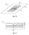
- Fig. 10 shows a security element 100 with a grid image according to the invention 101 and a partially applied thin-film structure 102.
- a paint was applied to a transparent film material 103, in which the word "PL" was introduced as a lattice image.
- a thin-film structure was vapor-deposited in the form of circles, which in this case consists of an absorber layer, a dielectric layer and a further absorber layer.
- Fig. 11 shows a further security element 110, in which on a carrier film 111, a resist layer 112 has been applied. A lattice image 116 was partially introduced into the lacquer layer. Above this there is an absorber layer 113 as well as a high refractive dielectric layer 114. A reflective layer 115 has been applied over this dielectric layer. The layers of the thin-film structure were evaporated by vacuum.
Description
Die Erfindung betrifft ein Gitterbild mit mehreren Gitterfeldern, die jeweils ein elektromagnetische Strahlung beeinflussendes Gittermuster aus einer Vielzahl von Strichgitterlinien enthalten, wobei die Strichgitterlinien durch die Parameter Orientierung, Krümmung, Beabstandung und Profilierung charakterisiert sind. Die Erfindung betrifft ferner ein Verfahren zum Herstellen eines solchen Gitterbildes sowie ein Sicherheitselement, ein Sicherheitspapier und einen Datenträger mit einem solchen Gitterbild.The invention relates to a lattice image with a plurality of lattice fields, each of which contains a lattice pattern influencing electromagnetic radiation from a multiplicity of lattice lines, the lattice lattice lines being characterized by the parameters orientation, curvature, spacing and profiling. The invention further relates to a method for producing such a grating image as well as a security element, a security paper and a data carrier with such a grating image.
Zur Echtheitsabsicherung von Kreditkarten, Banknoten und anderen Wertdokumenten werden seit einigen Jahren Hologramme, holographische Gitterbilder oder andere hologrammartige Beugungsstrukturen eingesetzt. Im Allgemeinen werden im Banknoten- und Sicherheitsbereich holographische Beugungsstrukturen verwendet, die sich durch Prägung von holographisch erzeugten Gitterbildern in thermoplastisch verformbare Kunststoffe oder UV-härtbare Lacke auf Foliensubstraten herstellen lassen.For authenticity assurance of credit cards, banknotes and other value documents, holograms, holographic lattice images or other hologram-like diffraction structures have been used for some years. In general, holographic diffraction structures are used in the banknote and security sector, which can be produced by embossing holographically generated lattice images in thermoplastically deformable plastics or UV-curable lacquers on film substrates.
Echte Hologramme entstehen durch Beleuchtung eines Objekts mit kohärentem Laserlicht und Überlagerung des von dem Objekt gestreuten Laserlichts mit einem unbeeinflussten Referenzstrahl in einer lichtempfindlichen Schicht. So genannte holographische Beugungsgitter erhält man, wenn die in der lichtempfindlichen Schicht überlagerten Lichtstrahlen aus räumlich ausgedehnten, einheitlichen kohärenten Wellenfeldern bestehen. Durch die Einwirkung der überlagerten Wellenfelder auf die lichtempfindliche Schicht, beispielsweise einen photographischen Film oder eine Photoresistschicht, entsteht dort ein holographisches Beugungsgitter, das in Form heller und dunkler Linien in einem photographischen Film oder in Form von Bergen und Tälern in einer Photoresistschicht konserviert werden kann. Da die Lichtstrahlen in diesem Fall nicht durch ein Objekt gestreut worden sind, erzeugt das holographische Beugungsgitter lediglich einen optisch variablen Farbeindruck, jedoch keine Bilddarstellung.Real holograms are formed by illuminating an object with coherent laser light and superposing the laser light scattered by the object with an uninfluenced reference beam in a photosensitive layer. So-called holographic diffraction gratings are obtained when the light beams superimposed in the photosensitive layer consist of spatially extended, uniform, coherent wave fields. The action of the superimposed wave fields on the photosensitive layer, for example a photographic film or a photoresist layer, produces a holographic diffraction grating in the form of light and dark lines in a photographic film or in the form of mountains and valleys in a photoresist layer can be preserved. Since the light rays have not been scattered by an object in this case, the holographic diffraction grating produces only an optically variable color impression, but no image representation.
Aus holographischen Beugungsgittern lassen sich holographische Gitterbilder erzeugen, indem nicht die gesamte Fläche des lichtempfindlichen Materials mit einem einheitlichen holographischen Beugungsgitter belegt wird, sondern indem geeignete Masken verwendet werden, um jeweils nur Teile der Aufnahmefläche mit einem von mehreren verschiedenen einheitlichen Gittermustern zu belegen. Ein solches holographisches Gitterbild setzt sich somit aus mehreren Gitterfeldern mit unterschiedlichen Beugungsgittermustern zusammen, die in der Regel nebeneinander in flächiger, streifenförmiger oder pixelartiger Ausführung liegen. Durch geeignete Anordnung der Gitterfelder lässt sich mit einem derartigen holographischen Gitterbild eine Vielzahl unterschiedlicher Bildmotive darstellen. Die Beugungsgittermuster können nicht nur durch direkte oder indirekte optische Überlagerung kohärenter Laserstrahlen, sondern auch mittels Elektronenlithographie hergestellt werden. Häufig wird eine Musterbeugungsstruktur erzeugt, die anschließend in eine Reliefstruktur umgesetzt wird. Diese Reliefstruktur kann als Prägewerkzeug verwendet werden.Holographic gratings can be generated from holographic diffraction gratings by not covering the entire surface of the photosensitive material with a uniform holographic diffraction grating, but by using suitable masks to respectively cover only parts of the receiving surface with one of several different uniform grating patterns. Such a holographic grating image is thus composed of a plurality of grating fields with different diffraction grating patterns, which are generally adjacent to one another in a flat, strip-shaped or pixel-like design. By suitable arrangement of the grating fields, a multiplicity of different image motifs can be represented with such a holographic grating image. The diffraction grating patterns can be produced not only by direct or indirect optical superposition of coherent laser beams but also by electron lithography. Frequently, a pattern diffraction structure is generated, which is subsequently converted into a relief structure. This relief structure can be used as a stamping tool.
Aus der Druckschrift
Die Druckschrift
Gegenstand der Druckschrift
Die Druckschrift
Die Druckschrift
Die Druckschrift
Davon ausgehend liegt der Erfindung die Aufgabe zugrunde, Gitterbilder der eingangs genannten Art weiter zu verbessern, und unter Beibehaltung der bisherigen Vorteile Gitterbilder mit neuen optischen Effekten zu schaffen und/oder die Fälschungssicherheit der Gitterbilder weiter zu erhöhen.On this basis, the present invention seeks to further improve lattice images of the type mentioned, and to create lattice images with new optical effects while maintaining the previous advantages and / or to further increase the anti-counterfeiting of the lattice images.
Diese Aufgabe wird durch das Gitterbild mit den Merkmalen des Hauptanspruchs gelöst. Ein Herstellungsverfahren sowie ein Sicherheitselement, ein Sicherheitspapier und ein Datenträger mit derartigen Gitterbildern sind in den nebengeordneten Ansprüchen angegeben. Weiterebildungen der Erfindung sind Gegenstand der Unteransprüche.This object is achieved by the grid image with the features of the main claim. A manufacturing method and a security element, a security paper and a data carrier with such grid images are given in the independent claims. Further developments of the invention are the subject of the dependent claims.
Die Erfindung baut auf dem Stand der Technik dadurch auf, dass ein mit bloßem Auge separat erkennbares Gitterfeld des Gitterbilds ein elektromagnetische Strahlung beeinflussendes Gittermuster mit Strichgitterlinien enthält, für die zumindest einer der charakteristischen Parameter Orientierung, Krümmung, Beabstandung und Profilierung über der Fläche des Gitterfelds variiert. Bevorzugt enthält das genannte Gitterfeld dabei ein elektromagnetische Strahlung beeinflussendes Gittermuster aus nicht unterbrochenen Strichgitterlinien.The invention is based on the state of the art in that a lattice field of the lattice image which can be separately recognized by the naked eye contains a lattice pattern with grating lines influencing electromagnetic radiation for which at least one of the characteristic parameters of orientation, curvature, spacing and profiling varies over the surface of the lattice field , Preferably, said grating field contains an electromagnetic radiation-influencing grating pattern of uninterrupted grating lines.
Im Rahmen der vorliegenden Beschreibung wird unter Beugung oder Diffraktion die Abweichung von der geradlinigen Ausbreitung des Lichts verstanden, die nicht durch Brechung, Reflexion oder Streuung hervorgerufen wird, sondern die auftritt, wenn Licht auf Hindernisse wie Spalte, Blenden oder Kanten trifft. Beugung ist eine typische Wellenerscheinung und daher stark wellenlängenabhängig und stets mit Interferenz verbunden. Sie ist insbesondere von den Vorgängen der Reflexion und der Brechung zu unterscheiden, die sich bereits mit dem Bild geometrischer Lichtstrahlen zutreffend beschreiben lassen. Hat man es mit Beugung an sehr vielen, statistisch verteilten Objekten zu tun, hat es sich eingebürgert, statt von Beugung an unregelmäßig verteilten Objekten von Streuung zu sprechen.In the present description diffraction or diffraction is understood to mean the deviation from the rectilinear propagation of the light which is not caused by refraction, reflection or scattering but that occurs when light hits obstacles such as gaps, apertures or edges. Diffraction is a typical wave phenomenon and therefore strongly wavelength dependent and always associated with interference. It is to be distinguished in particular from the processes of reflection and refraction, which can be accurately described with the image of geometric light rays. If one has to do with diffraction on very many statistically distributed objects, it has become customary to speak of diffraction instead of diffraction on irregularly distributed objects.
Unter Streuung versteht man die Ablenkung eines Teils einer gebündelten Wellerestrahlung aus seiner ursprünglichen Richtung beim Durchgang durch Materie aufgrund der Wechselwirkung mit einem oder mehreren Streuzentren. Die diffus in alle Raumrichtungen gestreute Strahlung bzw. die Gesamtheit der von den Streuzentren ausgehenden Streuwellen geht der primären Strahlung verloren. Streuung von Licht an Objekten mit einer Größenordnung im Bereich der Lichtwellenlänge und darunter ist in der Regel ebenfalls wellenlängenabhängig, wie beispielsweise die Rayleigh-Streuung oder die Mie-Streuung. Ab einer Objektgröße, die die zehnfache Wellenlänge überschreitet, spricht man gewöhnlich von nicht-selektiver Streuung, bei der alle Wellenlängen in etwa gleich beeinflusst werden.Scattering refers to the deflection of a portion of a collimated wave radiation from its original direction as it passes through matter due to interaction with one or more scattering centers. The radiation scattered diffusely in all spatial directions or the totality of the scattering waves emanating from the scattering centers is lost to the primary radiation. Scattering of light on objects of the order of wavelengths of light and below is also usually wavelength dependent, such as Rayleigh scattering or Mie scattering. From an object size exceeding ten times the wavelength, one usually speaks of non-selective scattering in which all wavelengths are affected approximately equally.
Nicht-selektive Streuung kann jedoch auch mit kleineren Objekten erreicht werden, wenn die Objekte nur eine unregelmäßige Verteilung und eine geeignete Bandbreite von Objektgrößen aufweisen, da sich dann die wellenlängenabhängigen Eigenschaften der einzelnen Objekte über das gesamte Ensemble herausmitteln.However, non-selective scattering can also be achieved with smaller objects if the objects have only an irregular distribution and a suitable bandwidth of object sizes, since then the wavelength-dependent properties of the individual objects are found out over the entire ensemble.
Nach der Erfindung weist der oder die variierenden charakteristischen. Parameter über die Fläche des Gitterfelds eine zufällige, insbesondere eine zufällige und sprunghafte Variation auf. Beispielsweise kann der Abstand der i-ten und (i+1)-ten Gitterlinie eines elektromagnetische Strahlung beeinflussenden Gittermusters durch die Beziehung ![]()
gegeben sein, wobei dmin und dmax wieder den minimalen bzw. maximalen Gitterlinienabstand und Rand() eine Zufallszahl oder geeignete erzeugte Pseudozufallszahl aus dem Intervall [0,1] darstellen. Der Abstand der Gitterlinien springt dann von Gitterlinie zu Gitterlinie willkürlich zwischen zufälligen Werten aus dem Intervall [dmin, dmax].According to the invention, the one or more varying characteristic. Parameter over the surface of the grid field on a random, in particular a random and sudden variation. For example, the distance of the i-th and (i + 1) th grid line of a grating pattern influencing electromagnetic radiation may be determined by the relationship ![]()
where dmin and dmax again represent the minimum and maximum grid line spacing, respectively, and Rand () represents a random number or suitable generated pseudo-random number from the interval [0,1]. The spacing of the grid lines then arbitrarily jumps from grid line to grid line arbitrarily between random values from the interval [dmin, dmax].
Der Bereich der Gitterlinienabstände liegt vorzugsweise zwischen etwa einem Zehntel und etwa dem Zehnfachen der Wellenlänge, für die das Gitterbild ausgelegt ist. Bei Gitterbildern, die für Betrachtung bei weißem Licht bestimmt, kann als Auslegungwellenlänge λ = 550 nm verwendet werden. Besonders bevorzugt sind Gitterlinenabstände, die zwischen etwa der Hälfte und etwa dem Doppelten der Auslegungswellenlänge liegen.The range of grid line spacings is preferably between about one tenth and about ten times the wavelength for which the grid image is designed. For grating images that are intended for white light viewing, λ = 550 nm can be used as the design wavelength. Particularly preferred are grid line spacings that are between about half and about twice the design wavelength.
In einer Weiterbildung der Erfindung enthält das genannte Gitterfeld ein weiteres elektromagnetische Strahlung beeinflussendes Gittermuster mit Strichgitterlinien, für die zumindest einer der charakteristischen Parameter Orientierung, Krümmung, Beabstandung und Profilierung über der Fläche des Gitterfelds variiert. Bevorzugt weisen die beiden elektromagnetische Strahlung beeinflussenden Gittermuster eine Variation in denselben Parametern auf. Die Strichgitterlinien der beiden elektromagnetische Strahlung beeinflussenden Gittermuster unterscheiden sich zweckmäßig durch einen nicht variierenden charakteristischen Parameter, insbesondere durch die Orientierung der Strichgitterlinien voneinander.In one development of the invention, said grating field contains a further grating pattern influencing electromagnetic radiation with grating lines for which at least one of the characteristic parameters of orientation, curvature, spacing and profiling varies over the surface of the grating field. Preferably, the two electromagnetic Radiation-influencing grid pattern on a variation in the same parameters. The grating lines of the two electromagnetic radiation influencing grid pattern differ appropriately by a non-varying characteristic parameter, in particular by the orientation of the grating lines from each other.
Erfindungsgemäß ist bei den beiden elektromagnetische Strahlung beeinflussenden Gittermustern jeweils die Beabstandung oder Krümmung zufällig variiert, und die Orientierung des zweiten elektromagnetische Strahlung beeinflussenden Gittermuster um einen bestimmten Winkel, etwa 90°, gegen die Orientierung des ersten elektromagnetische Strahlung beeinflussenden Gittermusters gedreht sein. Es versteht sich, dass das Gitterfeld auch mehr als zwei überlagerte elektromagnetische Strahlung beeinflussende Gittermuster enthalten kann.According to the invention, the spacing or curvature is randomly varied in each of the two electromagnetic patterns influencing the electromagnetic radiation, and the orientation of the second electromagnetic radiation-influencing grid pattern is rotated by a specific angle, approximately 90 °, against the orientation of the first electromagnetic radiation-influencing grid pattern. It is understood that the grating field can also contain more than two superposed electromagnetic radiation influencing grid pattern.
Das genannte Gitterfeld bildet eine Mattstruktur, die bei der Betrachtung keine diffraktiven Effekte zeigt. Dadurch können Flächenbereiche mit mattem Erscheinungsbild einfach in ein elektronenstrahllithographisch erzeugtes Gitterbild integriert werden. In einer zweckmäßigen Ausgestaltung sind die charakteristischen Parameter der Strichgitterlinien so variiert, dass die Mattstruktur keinerlei Farbigkeit zeigt. Der mit der Mattstruktur belegte Flächenbereich des Gitterbilds erscheint dann beispielsweise als metallischer, matter Bereich. In einer Weiterbildung dieser Ausführungsform weisen die Gitterbilder mit Mattstruktur unterschiedliche optische Helligkeit auf. In einer bevorzugten Variante lassen sich über die unterschiedlichen Helligkeiten Mattstrukturhalbtonbilder erzeugen, die insbesondere für die Darstellung von Portraits geeignet sind. Darüber hinaus kann durch genaue Einstellung der Helligkeit einzelner oder mehrerer Mattstrukturbereiche eine maschinenlesbare, optisch nicht erkennbare Kennzeichnung im Gitterbild erzeugt werden.The named grating field forms a matt structure, which shows no diffractive effects when viewed. As a result, areas with a matt appearance can be easily integrated into a grid image generated electron beam lithographically. In an expedient embodiment, the characteristic parameters of the grating lines are varied so that the matt structure shows no color. The surface area of the lattice image occupied by the matt structure then appears, for example, as a metallic, matt area. In a development of this embodiment, the grating images with a matt structure have different optical brightness. In a preferred variant, it is possible to generate matt-structure half-tone images over the different brightnesses, which are particularly suitable for portraits. About that In addition, by precise adjustment of the brightness of one or more matte structure areas, a machine-readable, optically unrecognizable marking can be generated in the lattice image.
In allen beschriebenen Gitterbildern sind die Strichgitterlinien mit Vorteil elektronenstrahllithographisch erzeugt. Diese Technik ermöglicht es, Gitterbilder herzustellen, bei denen jede einzelne Gitterlinie durch die Parameter Orientierung, Krümmung, Beabstandung und Profilierung eindeutig bestimmt werden kann.In all described grating images, the grating lines are advantageously produced by electron beam lithography. This technique makes it possible to produce grid images in which each individual grid line can be uniquely determined by the parameters orientation, curvature, spacing and profiling.
Es hat sich als zweckmäßig herausgestellt, wenn die Strichgitterlinien eine Linienprofiltiefe zwischen etwa 100 nm und etwa 400 nm aufweisen. Das Gitterbild selbst ist vorzugsweise mit einem reflektierenden oder hochbrechenden Material beschichtet. Als reflektierende Materialien kommen alle Metalle und viele Metalllegierungen in Betracht. Beispiele für geeignete hochbrechende Materialien sind CaS, CrO2, ZnS, TiO2 oder SiOx. Vorteilhaft besteht ein signifikanter Unterschied in den Brechungsindizes des Mediums, in das das Gitterbild eingebracht ist, und des hochbrechenden Materials, vorzugsweise ist die Differenz sogar größer als 0,5. Das Gitterbild kann in eingebetteter oder nicht eingebetteter Ausgestaltung erzeugt werden. Zur Einbettung eignen sich beispielsweise PVC, PET, Polyester oder eine UV-Lackschicht.It has been found to be useful if the grating lines have a line profile depth between about 100 nm and about 400 nm. The grating image itself is preferably coated with a reflective or high refractive index material. Reflective materials are all metals and many metal alloys into consideration. Examples of suitable high-index materials are CaS, CrO 2 , ZnS, TiO 2 or SiO x . Advantageously, there is a significant difference in the refractive indices of the medium into which the grating image is introduced and the high refractive index material, preferably the difference is even greater than 0.5. The grid image may be generated in embedded or non-embedded configuration. For embedding, for example, PVC, PET, polyester or a UV lacquer layer are suitable.
Die erfindungsgemäße Gestaltung der Gitterbilder ermöglicht neben neuartigen optischen Effekten auch eine eindeutig maschinenlesbare, optisch jedoch nicht sichtbare Kennzeichnung von hologrammartigen Gitterbildern. Beispielsweise können die Gitterbilder mit digitalen Wasserzeichen versehen werden. Die Fälschungssicherheit solcher Gitterbilder kann so deutlich erhöht werden.The inventive design of the lattice images allows not only novel optical effects but also a clearly machine-readable, but optically not visible marking of hologram-like lattice images. For example, the grid images may be provided with digital watermarks. The security against forgery of such lattice images can be significantly increased.
Die Erfindung umfasst auch Verfahren zum Herstellen von Gitterbildern, sowie ein Sicherheitselement mit einem Gitterbild der oben beschriebenen Art. Das Sicherheitselement kann insbesondere ein Sicherheitsfaden, ein Etikett oder ein Transferelement sein. Die Erfindung umfasst ferner ein Sicherheitspapier mit einem solchen Sicherheitselement sowie einen Datenträger, der mit einem Gitterbild, einem Sicherheitselement oder einem Sicherheitspapier der beschriebenen Art ausgestattet ist. Bei dem Datenträger kann es sich insbesondere um eine Banknote, ein Wertdokument, einen Pass, eine Ausweiskarte oder eine Urkunde handeln.The invention also includes methods for producing lattice images, as well as a security element with a lattice image of the type described above. The security element may in particular be a security thread, a label or a transfer element. The invention further comprises a security paper with such a security element and a data carrier which is equipped with a grid image, a security element or a security paper of the type described. In particular, the data carrier may be a banknote, a value document, a passport, an identity card or a certificate.
In einer weiteren Ausführungsform kann das erfindungsgemäße Gitterbild, mit einem farbkippenden Dünnschichtauf bau kombiniert werden. Dabei kann die Gesamtfläche des Gitterbildes oder auch nur eine Teilfläche des Gitterbildes mit dem Dünnschichtaufbau versehen werden. Der Dünnschichtaufbau kann je nach Anwendung opak oder auch semitransparent ausgeführt werden und umfasst mindestens drei Schichten. Beispielsweise kann der Schichtaufbau eine Reflexionsschicht, eine Absorberschicht und eine zwischen diesen beiden Schichten liegende Dielektrikumsschicht umfassen. Bei der Reflexionsschicht handelt es sich üblicherweise um eine Metallschicht, z.B. aus Aluminium. Alternativ besteht der Dünnschichtaufbau aus zwei Absorberschichten und einer zwischen den Absorberschichten liegenden Dielektrikumsschicht. Es ist auch denkbar, dass mehrere Absorber- und Dielektrikumsschichten alternierend vorliegen oder auch ausschließlich Dielektrikumsschichten vorgesehen sind, wobei aneinander grenzende Schichten stark unterschiedliche Brechungsindices besitzen, damit ein Farbkippeffekt erzeugt wird.In a further embodiment, the lattice image according to the invention can be combined with a Farbkippenden Dünnschichtauf construction. In this case, the total area of the lattice image or only a partial area of the lattice image can be provided with the thin-film structure. Depending on the application, the thin-film structure can be made opaque or semitransparent and comprises at least three layers. By way of example, the layer structure may comprise a reflection layer, an absorber layer and a dielectric layer lying between these two layers. The reflection layer is usually a metal layer, for example of aluminum. Alternatively exists the thin-film structure of two absorber layers and a lying between the absorber layers dielectric layer. It is also conceivable that a plurality of absorber and dielectric layers are present alternately or else only dielectric layers are provided, wherein adjacent layers have very different refractive indices, so that a color-shift effect is produced.
Als Absorberschichten dienen typischerweise Metallschichten aus Materialien, wie Chrom, Eisen, Gold, Aluminium oder Titan, in einer Dicke von vorzugsweise 4 nm bis 20 nm. Als Absorberschichtmaterialien können auch Verbindungen, wie Nickel-Chrom-Eisen, oder seltenere Metalle, wie Vanadium, Palladium oder Molybdän, verwendet werden. Weitere geeignete Materialien sind z.B. Nickel, Cobalt, Wolfram, Niobium, Aluminium, Metallverbindungen, wie Metallfluoride, -oxide, -sulfide, -nitride, -carbide, -phosphide, -selenide, -silicide und Verbindungen davon, aber auch Kohlenstoff, Germanium, Cermet und Eisenoxid. Die Absorberschichten können identisch sein, können aber auch unterschiedlich dick sein und/oder aus unterschiedlichem Material bestehen.As absorber layers are typically metal layers of materials such as chromium, iron, gold, aluminum or titanium, in a thickness of preferably 4 nm to 20 nm. As absorber layer materials can also compounds such as nickel-chromium-iron, or more rare metals such as vanadium, Palladium or molybdenum, can be used. Other suitable materials are e.g. Nickel, cobalt, tungsten, niobium, aluminum, metal compounds such as metal fluorides, oxides, sulfides, nitrides, carbides, phosphides, selenides, silicides and compounds thereof, but also carbon, germanium, cermet and iron oxide. The absorber layers may be identical, but may also be different in thickness and / or consist of different materials.
Für die Dielektrikumsschicht kommen hauptsächlich transparente Materialien mit einem niedrigen Brechungsindex < 1,7 in Betracht, wie beispielsweise SiO2, MgF, SiOx mit 1 < x < 2 und Al2O3. Grundsätzlich kommen fast alle aufdampfbaren, durchsichtigen Verbindungen infrage, insbesondere also auch höher brechende Beschichtungsmaterialien, wie ZrO2, ZnS, TiO2 und Indiumzinnoxide (ITO). Die Schichtdicke der Dielektrikumsschicht D liegt im Bereich von 100 nm bis 1000 nm, bevorzugt 200 nm bis 500 nm.For the dielectric layer are mainly transparent materials with a low refractive index <1.7 into consideration, such as SiO 2 , MgF, SiO x with 1 <x <2 and Al 2 O 3 . In principle, almost all vapor-deposited, transparent compounds are suitable, in particular also higher-refractive coating materials such as ZrO 2 , ZnS, TiO 2 and indium tin oxides (ITO). The layer thickness of the dielectric layer D is in the range of 100 nm to 1000 nm, preferably 200 nm to 500 nm.
Unterschiedlichste Bedampfungsverfahren sind zur Erzeugung der Schichten geeignet. Eine methodische Gruppe bildet Physical Vapor Deposition (PVD) mit Schiffchenbedampfung, Bedampfung durch Widerstandsheizung, Bedampfung durch Induktionsheizung oder auch Elektronenstrahlbedampfung, Sputtern (DC oder AC) und Lichtbogenbedampfung. Andererseits kann die Bedampfung auch als Chemical Vapor Deposition (CVD) erfolgen, wie z.B. Sputter im reaktiven Plasma oder jede andere plasmaunterstützte Bedampfungsart. Es besteht grundsätzlich auch die die Möglichkeit, Dielektrikumsschichten aufzudrucken.Different steaming processes are suitable for producing the layers. A methodological group is Physical Vapor Deposition (PVD) with Schiffchenbedampfung, evaporation by resistance heating, vapor deposition by induction heating or electron beam evaporation, sputtering (DC or AC) and arc vapor deposition. On the other hand, the vapor deposition can also take place as chemical vapor deposition (CVD), such as e.g. Sputter in the reactive plasma or any other plasma-assisted evaporation method. In principle, it is also possible to print on dielectric layers.
Die Kombination von Mattstrukturen und farbkippenden Dünnschichtaufbauten ist sehr schwer zu fälschen, da die Technologien zur Herstellung dieser Elemente äußerst schwer zu beschaffen sind. Darüber hinaus kann das Design der Mattstruktur und des Dünnschichtaufbaus aufeinander genau abgestimmt werden, so dass völlig neuartige optische Effekte erzielt werden können.The combination of matt structures and color-shifting thin-film structures is very difficult to falsify, as the technologies for producing these elements are extremely difficult to obtain. In addition, the design of the matt structure and the thin-film structure can be precisely coordinated with each other, so that completely new optical effects can be achieved.
Weitere Ausführungsbeispiele sowie Vorteile der Erfindung werden nachfolgend anhand der Figuren erläutert. Zur besseren Anschaulichkeit ist in den Figuren auf eine maßstabs- und proportionsgetreue Darstellung verzichtet.Further embodiments and advantages of the invention are explained below with reference to the figures. For better clarity is omitted in the figures on a scale and proportionate representation.
Es zeigen:
- Fig. 1
- eine schematische Darstellung einer Banknote mit eingebettetem Sicherheitsfaden und aufgeklebtem Transferelement, jeweils nach einem Ausführungsbeispiel der Erfindung,
- Fig. 2
- in (a) ein Gitterbild mit drei Gitterfeldern in schematischer Darstellung, wobei in (b) die Belegung der Gitterfelder mit verschiedenen elektromagnetische Strahlung beeinflussenden Gittermustern angedeutet ist,
- Fig. 3
- in (a) und (b) je eine Detailaufsicht auf ein Gitterfeld mit einem elektromagnetis che Strahlung beeinflussenden Gittermuster, für dessen Strichgitterlinien der Parameter Beabstandung über der Fläche des Gitterfelds kontinuierlich varüert,
- Fig. 4
- in (a) und (b) je eine Detailaufsicht auf ein Gitterfeld mit einem elektromagnetis che Strahlung beeinflussenden Gittermuster, für dessen Strichgitterlinien der Parameter Krümmung über der Fläche des Gitterfelds kontinuierlich variiert,
- Fig. 5
- in (a) und (b) je eine Detailaufsicht auf ein Gitterfeld mit einem elektromagnetische Strahlung beeinflussenden Gittermuster, für dessen Strichgitterlinien der Parameter Orientierung über der Fläche des Gitterfelds kontinuierlich variiert,
- Fig. 6 bis 8
- jeweils Detailaufsichten auf erfindungsgemäße Gitterfelder mit elektromagnetische Strahlung beeinfLussenden Gittermustern, für deren Strichgitterlinien einer der charakteristischen Parameter zufällig und sprunghaft variiert,
- Fig. 9
- zwei Detailaufsichten auf den Übergang zwischen zwei aneinander grenzenden Gitterfeldern, wobei in (a) ein herkömmlicher diskontinuierlicher Übergang und in (b) ein kontinuierlicher Übergang gezeigt ist,
- Fig. 10
- eine Aufsicht auf ein Sicherheitselement mit Dürnschichtaufbau, und
- Fig.11
- einen Querschnitt durch ein Sicherheitselement mit Dünnschichtaufbau.
- Fig. 1
- a schematic representation of a banknote with embedded security thread and glued transfer element, each according to an embodiment of the invention,
- Fig. 2
- in (a) a lattice image with three lattice fields in a schematic representation, wherein in (b) the assignment of the lattice fields with different electromagnetic radiation influencing lattice patterns is indicated,
- Fig. 3
- in (a) and (b) each have a detailed supervision of a grid field with a grid pattern influencing electromagnetic radiation, for whose grid lines the parameter spacing continuously varies across the area of the grid field,
- Fig. 4
- in (a) and (b) each have a detailed supervision of a grid field with a grid pattern influencing electromagnetic radiation, for whose grid lines the parameter curvature continuously varies over the area of the grid field,
- Fig. 5
- in (a) and (b), respectively, detail monitoring of a grating field with a grating pattern influencing electromagnetic radiation, for whose grating lines the parameter orientation varies continuously over the surface of the grating field,
- Fig. 6 to 8
- detail views of lattice fields according to the invention with lattice patterns influencing electromagnetic radiation, for the lattice lines of which one of the characteristic parameters varies randomly and suddenly,
- Fig. 9
- two detailed views of the transition between two adjoining grid fields, showing in (a) a conventional discontinuous transition and in (b) a continuous transition,
- Fig. 10
- a view of a security element with Dürnschichtaufbau, and
- Figure 11
- a cross section through a security element with thin-film construction.
Die allgemeine Gestalt eines hologrammartigen Gitterbilds ist in der
Die Strichgitterlinien 24 jedes elektromagnetische Strahlung beeinflussenden Gittermusters können durch vier charakteristische Parameter, nämlich durch ihre Orientierung, Krümmung, Beabstandung und die Profilierung der einzelnen Linien, beschrieben werden. An der Grenzlinie 26 zwischen zwei aneinander grenzenden Gitterfeldern ergibt sich üblicherweise eine Diskontinuität im Bezug auf zumindest einen der genannten Parameter. Beispielsweise sind die Strichgitterlinien 24 und 24-1 der Gitterfelder 22 und 22-1 beide gerade und mit sinoidaler Profilierung (in
Die
Wie aus
In
Als weiteres illustrierendes Beispiel zeigt
Auch das Gitterfeld 40 ist, wie die nachfolgend in den
Bei dem illustrierenden Beispiel der
Die Detailaufsicht der
Bei dem Ausführungsbeispiel der
Die Detailaufsicht der
Lässt sich, wie bei dieser speziellen Ausführungsform, ein Zusammenhang zwischen Helligkeit der mit elektromagnetische Strahlung beeinflussenden Gittern bedeckten Fläche und geeigneten geometrischen Parametern herstellen, so kann sogar die relative Helligkeit der entsprechenden Flächenbereiche gezielt variiert werden. Die Gitterstruktur in
Neben der in den
Es versteht sich weiter, dass nicht nur einer der charakteristischen Parameter über die Fläche des Gitterfelds variiert werden kann, sondern auch mehrere Parameter gleichzeitig. Beispielsweise können die Strichgitterlinien in einem Gitterfeld zugleich in den Parametern Beabstandung, Orientierung und Profilierung variieren.It is further understood that not only one of the characteristic parameters can be varied over the area of the grid field, but also several parameters simultaneously. For example, the grating lines in a grating field can vary at the same time in the parameters of spacing, orientation and profiling.
Alle beschriebenen elektromagnetische Strahlung beeinflussenden Gittermuster lassen sich mittels Elektronenstrahllithographie erzeugen. Diese Technik ermöglicht es, Gitterbilder herzustellen, bei denen im Extremfall jede einzelne Linie eines Strichgitters durch die genannten charakteristischen Parameter eindeutig bestimmt werden kann.All described electromagnetic radiation influencing grid pattern can be generated by electron beam lithography. This technique makes it possible to produce lattice images in which, in extreme cases, each individual line of a lattice grating can be uniquely determined by said characteristic parameters.
Während die
Das elektromagnetische Strahlung beeinflussende Gittermuster des ersten Gitterfelds 90 wird sich im Allgemeinen in einem oder mehreren der charakteristischen Parameter von dem elektromagnetische Strahlung beeinflussenden Gittermuster des zweiten Gitterfelds 92 unterscheiden. Im Beispiel der
Zur Abhilfe ist zwischen dem ersten Gitterfeld 90 und dem zweiten Gitterfeld 92 einen Übergangsbereich 96 vor gesehen, in dem die charakteristischen Parameter der Strichgitterlinien des ersten Gitterfelds kontinuierlich in die charakteristischen Parameter der Strichgitterlinien des zweiten Gitterfelds übergehen. Derartige weiche Übergänge können ohne Unterbrechung der Strichgitterlinien mit Elektronenstrahllithographie in vergleichsweise einfacher Weise realisiert werden.As a remedy, a
Bezüglich der Längenskala, auf der der Übergang erfolgt, bestehen für den Designer zwei Möglichkeiten. Lässt man den Übergang zwischen den elektromagnetische Strahlung beeinflussende Gittermuster der beiden Gitterfelder auf einer Längenskala von etwa 100 µm oder weniger erfolgen, so kann der Betrachter den Übergangsbereich mit bloßem Auge nicht erfassen. Es werden somit lediglich die störenden optischen Artefakte an der Grenzlinie der beiden Gitterfelder beseitigt.Regarding the length scale on which the transition occurs, the designer has two options. Allowing the transition between the electromagnetic radiation influencing grid pattern of the two grating fields on a length scale of about 100 microns or less, so the viewer can not capture the transition region with the naked eye. It Thus, only the disturbing optical artifacts are eliminated at the boundary line of the two grating fields.
Lässt man andererseits den Übergang auf einer Längenskala von mehr als 100 µm erfolgen, so kann der Übergangsbereich vom Betrachter wahrgenommen werden. Dies kann ausgenutzt werden, um neuartige optische Effekte im Übergang zweier Gitterfelder zu erzeugen.On the other hand, if the transition is made on a length scale of more than 100 μm, the transitional area can be perceived by the viewer. This can be exploited to create novel optical effects in the transition of two grating fields.
Claims (17)
- A grating image having multiple grating fields, each of which includes an electromagnetic-radiation-influencing grating pattern comprising a plurality of grating lines, the grating lines being characterized by the parameters orientation, curvature, spacing and profile, characterized in that,- in the grating image, a grating field that is separately perceptible with the naked eye includes an electromagnetic radiation-influencing grating pattern having grating lines for which at least one of the characteristic parameters orientation, curvature, spacing and profile varies across the surface of the grating field,- said grating field forms a matte pattern that displays no diffractive effects when viewed, and- the varying characteristic parameter(s) exhibit a random variation across the surface of the grating field.
- The grating image according to claim 1, characterized in that said grating field includes an electromagnetic radiation-influencing grating pattern comprising uninterrupted grating lines.
- The grating image according to claim 1 or 2, characterized in that the varying characteristic parameter(s) exhibit a random and discontinuous variation across the surface of the grating field.
- The grating image according to at least one of claims 1 to 3, characterized in that said grating field includes at least one further electromagnetic radiation-influencing grating pattern having grating lines for which at least one of the characteristic parameters orientation, curvature, spacing and profile varies across the surface of the grating field.
- The grating image according to claim 4, characterized in that the electromagnetic radiation-influencing grating patterns exhibit a variation in those same parameters.
- The grating image according to claim 4 or 5, characterized in that the grating lines of the electromagnetic radiation-influencing grating pattern differ from one another by a non-varying characteristic parameter, especially by the orientation of the grating lines.
- The grating image according to at least one of claims 1 to 6, characterized in that the grating fields exhibit different optical brightness.
- The grating image according to at least one of claims 1 to 7, characterized in that the grating lines exhibit a line profile depth between about 100 nm and about 400 nm.
- The grating image according to at least one of claims 1 to 8, characterized in that the grating image is coated with a reflecting or high-index material.
- The grating image according to at least one of claims 1 to 9, characterized in that the grating image includes a machine-readable identifier that is not visible with the naked eye.
- The grating image according to at least one of claims 1 to 10, characterized in that the grating image is combined with a color-shifting thin-film structure.
- A method for manufacturing a grating image, in which are produced in a substrate multiple grating fields, each of which is filled with an electromagnetic radiation-influencing grating pattern comprising a plurality of grating lines, the grating lines being characterized by the parameters orientation, curvature, spacing and profile, characterized in that,- in the grating image, a grating field that is separately perceptible with the naked eye is filled with an electromagnetic radiation-influencing grating pattern having grating lines for which at least one of the characteristic parameters orientation, curvature, spacing and profile is varied across the surface of the grating field,- said grating field forms a matte pattern that displays no diffractive effects when viewed, and- the varying characteristic parameter(s) exhibit a random variation across the surface of the grating field.
- A security element having a grating image according to at least one of claims 1 to 11.
- The security element according to claim 13, characterized in that the security element is a security thread, a label or a transfer element.
- A security paper having a security element according to claim 13 or 14.
- A data carrier having a grating image according to at least one of claims 1 to 11, a security element according to claim 13 or 14, or a security paper according to claim 15.
- The data carrier according to claim 16, characterized in that the data carrier is a banknote, a value document, a passport, an identification card or a certificate.
Applications Claiming Priority (2)
| Application Number | Priority Date | Filing Date | Title |
|---|---|---|---|
| DE102004003984A DE102004003984A1 (en) | 2004-01-26 | 2004-01-26 | Lattice image with one or more grid fields |
| PCT/EP2005/000659 WO2005071444A2 (en) | 2004-01-26 | 2005-01-24 | Grid image with one or several varied grid fields |
Publications (3)
| Publication Number | Publication Date |
|---|---|
| EP1713645A2 EP1713645A2 (en) | 2006-10-25 |
| EP1713645B1 true EP1713645B1 (en) | 2014-04-30 |
| EP1713645B2 EP1713645B2 (en) | 2024-01-03 |
Family
ID=34745158
Family Applications (1)
| Application Number | Title | Priority Date | Filing Date |
|---|---|---|---|
| EP05701144.7A Active EP1713645B2 (en) | 2004-01-26 | 2005-01-24 | Grid image with several grid fields |
Country Status (7)
| Country | Link |
|---|---|
| US (1) | US7710652B2 (en) |
| EP (1) | EP1713645B2 (en) |
| CN (1) | CN100489568C (en) |
| DE (1) | DE102004003984A1 (en) |
| RU (1) | RU2370376C2 (en) |
| UA (1) | UA87482C2 (en) |
| WO (1) | WO2005071444A2 (en) |
Families Citing this family (24)
| Publication number | Priority date | Publication date | Assignee | Title |
|---|---|---|---|---|
| DE102005032997A1 (en) | 2005-07-14 | 2007-01-18 | Giesecke & Devrient Gmbh | Lattice image and method for its production |
| DE102006012732A1 (en) | 2006-03-17 | 2007-09-20 | Giesecke & Devrient Gmbh | grid image |
| EP1855127A1 (en) | 2006-05-12 | 2007-11-14 | Rolic AG | Optically effective surface relief microstructures and method of making them |
| DE102007009646A1 (en) | 2007-02-26 | 2008-08-28 | Giesecke & Devrient Gmbh | Holographic grid image for security element of e.g. bank note, has grid fields which are achromatic grid fields, and formed of sub-ranges overlapping with one another, where dimension of sub-ranges lies below resolution limit of naked eye |
| GB0711434D0 (en) | 2007-06-13 | 2007-07-25 | Rue De Int Ltd | Holographic security device |
| DE102007039591A1 (en) | 2007-08-22 | 2009-02-26 | Giesecke & Devrient Gmbh | grid image |
| KR101105912B1 (en) | 2008-04-18 | 2012-01-17 | 도판 인사츠 가부시키가이샤 | Labeling material and labeled goods item |
| DE102008049513A1 (en) | 2008-09-29 | 2010-04-01 | Giesecke & Devrient Gmbh | Lattice image with achromatic lattice fields |
| JPWO2010064344A1 (en) * | 2008-12-04 | 2012-05-10 | パナソニック株式会社 | Exterior parts and manufacturing method thereof |
| FR2945159B1 (en) * | 2009-04-29 | 2016-04-01 | Horiba Jobin Yvon Sas | REFLECTIVE METAL DIFFRACTION NETWORK HAVING A HIGH FLOW OF FEMTOSECOND FLOW, SYSTEM COMPRISING SUCH A NETWORK AND METHOD FOR IMPROVING THE DAMAGE THRESHOLD OF A METAL DIFFRACTION NETWORK |
| DE102009049222A1 (en) | 2009-10-13 | 2011-04-28 | Giesecke & Devrient Gmbh | Lattice image with adjoining grid fields |
| EP2336823A1 (en) * | 2009-12-18 | 2011-06-22 | Boegli-Gravures S.A. | Method and device for producing masks for a laser assembly for generating microstructures |
| EP2441593B1 (en) | 2010-10-13 | 2020-04-15 | Hueck Folien Gesellschaft m.b.H. | Security element with achromatic features |
| DE102010050105A1 (en) * | 2010-10-29 | 2012-05-03 | Giesecke & Devrient Gmbh | Lattice image with adjoining grid fields |
| DE102011011349A1 (en) | 2011-02-16 | 2012-08-16 | Giesecke & Devrient Gmbh | Lattice image with arch effect |
| DE102011016050A1 (en) * | 2011-04-04 | 2012-10-04 | Schreiner Group Gmbh & Co. Kg | Optically variable security feature |
| KR20140033452A (en) * | 2011-06-23 | 2014-03-18 | 도요세이칸 그룹 홀딩스 가부시키가이샤 | Structure, structure-forming method, and structure-forming device |
| DE102011115589A1 (en) * | 2011-10-11 | 2013-04-11 | Giesecke & Devrient Gmbh | security element |
| CZ2012524A3 (en) * | 2012-07-31 | 2013-09-18 | Iq Structures S.R.O. | Diffractive element and method of making such diffractive element |
| GB201400910D0 (en) | 2014-01-20 | 2014-03-05 | Rue De Int Ltd | Security elements and methods of their manufacture |
| CN107924001B (en) | 2015-08-07 | 2021-06-04 | 罗利克技术有限公司 | Orientation-modulated scattering device |
| RU178207U1 (en) * | 2017-02-27 | 2018-03-26 | Алексей Алексеевич Гришаков | Label to protect product packaging from counterfeiting and attract customer attention |
| DE102017008918A1 (en) | 2017-09-22 | 2019-03-28 | Giesecke+Devrient Currency Technology Gmbh | Platelet-shaped pigment, printing ink, security element and manufacturing process |
| DE102018119706B4 (en) * | 2018-08-14 | 2022-04-28 | Laser-Laboratorium Göttingen e.V. | Information carrier and method for its production |
Family Cites Families (35)
| Publication number | Priority date | Publication date | Assignee | Title |
|---|---|---|---|---|
| DE2853953A1 (en) * | 1978-12-14 | 1980-07-03 | Hoechst Ag | IDENTIFICATION CARD |
| DE3130182A1 (en) | 1981-07-30 | 1983-02-17 | GAO Gesellschaft für Automation und Organisation mbH, 8000 München | Guilloche grid |
| GB2136352B (en) | 1982-12-03 | 1986-09-10 | Hollusions Limited | Hologram devices and methods of manufacture |
| US4818852A (en) * | 1986-01-24 | 1989-04-04 | Drexler Technology Corporation | Method for forming data cards with registered images |
| EP0330738B1 (en) † | 1988-03-03 | 1991-11-13 | Landis & Gyr Betriebs AG | Document |
| EP0366858B1 (en) † | 1988-09-30 | 1995-08-02 | Landis & Gyr Technology Innovation AG | Bar code field and bar code reader |
| DE58906429D1 (en) † | 1988-09-30 | 1994-01-27 | Landis & Gyr Business Support | Diffraction element. |
| US5003600A (en) † | 1989-08-03 | 1991-03-26 | The United States Of America As Represented By The Department Of Energy | Diffraction gratings used as identifying markers |
| US5291317A (en) | 1990-07-12 | 1994-03-01 | Applied Holographics Corporation | Holographic diffraction grating patterns and methods for creating the same |
| DE4132476A1 (en) | 1991-09-30 | 1993-04-01 | Matthiesen Geb Sievers Gerda | Hologram printing on paper or cardboard at high speeds - has varnish layer on web print material to be hardened by UV setting |
| DE4133620C1 (en) | 1991-10-10 | 1993-04-22 | Maho Ag, 8962 Pfronten, De | |
| US5759430A (en) * | 1991-11-27 | 1998-06-02 | Tapscott; Robert E. | Clean, tropodegradable agents with low ozone depletion and global warming potentials to protect against fires and explosions |
| DE4243905A1 (en) * | 1992-12-23 | 1994-06-30 | Gao Ges Automation Org | Security element to protect security documents against reproduction |
| US6088161A (en) † | 1993-08-06 | 2000-07-11 | The Commonwealth Of Australia Commonwealth Scientific And Industrial Research Organization | Diffractive device having a surface relief structure which generates two or more diffraction images and includes a series of tracks |
| TW275109B (en) * | 1993-08-06 | 1996-05-01 | Commw Scient Ind Res Org | |
| EP0712012A1 (en) † | 1994-11-09 | 1996-05-15 | International Business Machines Corporation | Authentication label and authenticating pattern incorporating diffracting structure and method of fabricating them |
| CH690067A5 (en) | 1995-08-10 | 2000-04-14 | Ovd Kinegram Ag | A process for preparing teilmetallisierter lattice structures. |
| PL177897B1 (en) | 1995-10-31 | 2000-01-31 | Remigiusz Gajda | Optically variable elements as well as method of and apparatus for recording thereon |
| SI0868313T1 (en) † | 1995-11-28 | 2001-02-28 | Ovd Kinegram Ag | Optically variable surface pattern |
| CH693316A5 (en) † | 1998-01-27 | 2003-05-30 | Ovd Kinegram Ag | Surface patterns with superimposed diffraction gratings. |
| GB9810399D0 (en) | 1998-05-14 | 1998-07-15 | Rue De Int Ltd | Holographic security device |
| AUPP444498A0 (en) * | 1998-07-02 | 1998-07-23 | Commonwealth Scientific And Industrial Research Organisation | Diffractive structure with interstitial elements |
| AUPQ128899A0 (en) * | 1999-06-30 | 1999-07-22 | Securency Pty Ltd | Security article including diffractive optic filter |
| ATE369592T1 (en) † | 2000-04-15 | 2007-08-15 | Ovd Kinegram Ag | SURFACE PATTERN |
| DE10148122A1 (en) † | 2001-09-28 | 2003-04-24 | Giesecke & Devrient Gmbh | security paper |
| ATE427837T1 (en) † | 2001-12-22 | 2009-04-15 | Ovd Kinegram Ag | DIFFRACTIVE SAFETY ELEMENT |
| DE10206357A1 (en) † | 2002-02-14 | 2003-08-28 | Giesecke & Devrient Gmbh | Security element and security document with such a security element |
| DE10216563B4 (en) † | 2002-04-05 | 2016-08-04 | Ovd Kinegram Ag | Security element as photocopy protection |
| CN100534806C (en) † | 2002-05-14 | 2009-09-02 | 雷恩哈德库兹两合公司 | Optically variable element comprising a sequence of thin-film layers |
| KR100660468B1 (en) † | 2002-05-14 | 2006-12-22 | 레오나르트 쿠르츠 게엠베하 운트 코. 카게 | Optically variable element comprising a partially transparent element |
| DE10221491A1 (en) † | 2002-05-14 | 2003-12-04 | Kurz Leonhard Fa | Optically variable surface pattern |
| US6815065B2 (en) * | 2002-05-31 | 2004-11-09 | Flex Products, Inc. | All-dielectric optical diffractive pigments |
| WO2003107047A1 (en) † | 2002-06-12 | 2003-12-24 | Giesecke & Devrient Gmbh | Method for producing grating images |
| DE10243413A1 (en) † | 2002-06-12 | 2003-12-24 | Giesecke & Devrient Gmbh | Process for the production of grid images |
| DE10226115A1 (en) | 2002-06-12 | 2003-12-24 | Giesecke & Devrient Gmbh | Process for generating a grid picture, grid picture and security document |
-
2004
- 2004-01-26 DE DE102004003984A patent/DE102004003984A1/en not_active Withdrawn
-
2005
- 2005-01-24 RU RU2006131412/12A patent/RU2370376C2/en active
- 2005-01-24 WO PCT/EP2005/000659 patent/WO2005071444A2/en active Application Filing
- 2005-01-24 UA UAA200608340A patent/UA87482C2/en unknown
- 2005-01-24 CN CNB2005800023267A patent/CN100489568C/en not_active Expired - Fee Related
- 2005-01-24 US US10/587,294 patent/US7710652B2/en active Active
- 2005-01-24 EP EP05701144.7A patent/EP1713645B2/en active Active
Also Published As
| Publication number | Publication date |
|---|---|
| WO2005071444A3 (en) | 2006-05-11 |
| US20070109532A1 (en) | 2007-05-17 |
| CN1938164A (en) | 2007-03-28 |
| DE102004003984A1 (en) | 2005-08-11 |
| EP1713645B2 (en) | 2024-01-03 |
| EP1713645A2 (en) | 2006-10-25 |
| CN100489568C (en) | 2009-05-20 |
| RU2370376C2 (en) | 2009-10-20 |
| RU2006131412A (en) | 2008-03-10 |
| WO2005071444A2 (en) | 2005-08-04 |
| UA87482C2 (en) | 2009-07-27 |
| US7710652B2 (en) | 2010-05-04 |
Similar Documents
| Publication | Publication Date | Title |
|---|---|---|
| EP1713645B1 (en) | Grid image with several grid fields | |
| EP1999726B1 (en) | Grating image | |
| EP2114673B1 (en) | Security document | |
| EP1800271B1 (en) | Security document | |
| EP2632739B1 (en) | Security element having optically variable surface pattern | |
| EP2155963B2 (en) | Inspection security element | |
| EP3337674B1 (en) | Valuable document | |
| EP3339048A1 (en) | Security element having reflective surface area | |
| DE102006016139A1 (en) | Multi-layer body with volume hologram | |
| EP2198407A1 (en) | Grid image | |
| WO2004077468A2 (en) | Safety element | |
| EP2335100B1 (en) | Grid image having achromatic grid fields | |
| WO2004076197A2 (en) | Safety element | |
| EP1547807B1 (en) | Security element having a diffraction structure and method of manufacturing said element | |
| EP2593310B1 (en) | Security element with hologram structures | |
| EP3406458B1 (en) | Security element with reflective surface area | |
| EP2312345B1 (en) | Diffraction grating image with adjoining grating fields | |
| EP2207051A1 (en) | Safety element and method for manufacturing a safety element | |
| EP4353486A2 (en) | Security element with refractive structures and colour change | |
| EP2633347A1 (en) | Grating image having mutually adjoining grating fields | |
| DE202004019437U1 (en) | Optical security element for credit card, cash card or banknote, has diffractive structure between two transparent layers of different refractive index |
Legal Events
| Date | Code | Title | Description |
|---|---|---|---|
| PUAI | Public reference made under article 153(3) epc to a published international application that has entered the european phase |
Free format text: ORIGINAL CODE: 0009012 |
|
| AK | Designated contracting states |
Kind code of ref document: A2 Designated state(s): AT BE BG CH CY CZ DE DK EE ES FI FR GB GR HU IE IS IT LI LT LU MC NL PL PT RO SE SI SK TR |
|
| AX | Request for extension of the european patent |
Extension state: AL BA HR LV MK YU |
|
| 17P | Request for examination filed |
Effective date: 20061113 |
|
| RBV | Designated contracting states (corrected) |
Designated state(s): AT BE BG CH CY CZ DE DK EE ES FI FR GB GR HU IE IS IT LI LT LU MC NL PL PT RO SE SI SK TR |
|
| DAX | Request for extension of the european patent (deleted) | ||
| 17Q | First examination report despatched |
Effective date: 20120109 |
|
| GRAP | Despatch of communication of intention to grant a patent |
Free format text: ORIGINAL CODE: EPIDOSNIGR1 |
|
| RIC1 | Information provided on ipc code assigned before grant |
Ipc: B42D 15/00 20060101AFI20131105BHEP Ipc: G02B 5/18 20060101ALI20131105BHEP Ipc: G07D 7/00 20060101ALI20131105BHEP |
|
| INTG | Intention to grant announced |
Effective date: 20131128 |
|
| GRAS | Grant fee paid |
Free format text: ORIGINAL CODE: EPIDOSNIGR3 |
|
| GRAA | (expected) grant |
Free format text: ORIGINAL CODE: 0009210 |
|
| STAA | Information on the status of an ep patent application or granted ep patent |
Free format text: STATUS: THE PATENT HAS BEEN GRANTED |
|
| AK | Designated contracting states |
Kind code of ref document: B1 Designated state(s): AT BE BG CH CY CZ DE DK EE ES FI FR GB GR HU IE IS IT LI LT LU MC NL PL PT RO SE SI SK TR |
|
| REG | Reference to a national code |
Ref country code: GB Ref legal event code: FG4D Free format text: NOT ENGLISH Ref country code: CH Ref legal event code: EP |
|
| REG | Reference to a national code |
Ref country code: DE Ref legal event code: R081 Ref document number: 502005014322 Country of ref document: DE Owner name: GIESECKE+DEVRIENT CURRENCY TECHNOLOGY GMBH, DE Free format text: FORMER OWNER: GIESECKE & DEVRIENT GMBH, 81677 MUENCHEN, DE |
|
| REG | Reference to a national code |
Ref country code: AT Ref legal event code: REF Ref document number: 664833 Country of ref document: AT Kind code of ref document: T Effective date: 20140515 |
|
| REG | Reference to a national code |
Ref country code: IE Ref legal event code: FG4D Free format text: LANGUAGE OF EP DOCUMENT: GERMAN |
|
| REG | Reference to a national code |
Ref country code: DE Ref legal event code: R096 Ref document number: 502005014322 Country of ref document: DE Effective date: 20140612 |
|
| REG | Reference to a national code |
Ref country code: CH Ref legal event code: NV Representative=s name: RENTSCH PARTNER AG, CH |
|
| REG | Reference to a national code |
Ref country code: LT Ref legal event code: MG4D |
|
| REG | Reference to a national code |
Ref country code: NL Ref legal event code: VDEP Effective date: 20140430 |
|
| PG25 | Lapsed in a contracting state [announced via postgrant information from national office to epo] |
Ref country code: BG Free format text: LAPSE BECAUSE OF FAILURE TO SUBMIT A TRANSLATION OF THE DESCRIPTION OR TO PAY THE FEE WITHIN THE PRESCRIBED TIME-LIMIT Effective date: 20140730 Ref country code: CY Free format text: LAPSE BECAUSE OF FAILURE TO SUBMIT A TRANSLATION OF THE DESCRIPTION OR TO PAY THE FEE WITHIN THE PRESCRIBED TIME-LIMIT Effective date: 20140430 Ref country code: GR Free format text: LAPSE BECAUSE OF FAILURE TO SUBMIT A TRANSLATION OF THE DESCRIPTION OR TO PAY THE FEE WITHIN THE PRESCRIBED TIME-LIMIT Effective date: 20140731 Ref country code: IS Free format text: LAPSE BECAUSE OF FAILURE TO SUBMIT A TRANSLATION OF THE DESCRIPTION OR TO PAY THE FEE WITHIN THE PRESCRIBED TIME-LIMIT Effective date: 20140830 Ref country code: FI Free format text: LAPSE BECAUSE OF FAILURE TO SUBMIT A TRANSLATION OF THE DESCRIPTION OR TO PAY THE FEE WITHIN THE PRESCRIBED TIME-LIMIT Effective date: 20140430 Ref country code: LT Free format text: LAPSE BECAUSE OF FAILURE TO SUBMIT A TRANSLATION OF THE DESCRIPTION OR TO PAY THE FEE WITHIN THE PRESCRIBED TIME-LIMIT Effective date: 20140430 Ref country code: NL Free format text: LAPSE BECAUSE OF FAILURE TO SUBMIT A TRANSLATION OF THE DESCRIPTION OR TO PAY THE FEE WITHIN THE PRESCRIBED TIME-LIMIT Effective date: 20140430 |
|
| PG25 | Lapsed in a contracting state [announced via postgrant information from national office to epo] |
Ref country code: PL Free format text: LAPSE BECAUSE OF FAILURE TO SUBMIT A TRANSLATION OF THE DESCRIPTION OR TO PAY THE FEE WITHIN THE PRESCRIBED TIME-LIMIT Effective date: 20140430 Ref country code: ES Free format text: LAPSE BECAUSE OF FAILURE TO SUBMIT A TRANSLATION OF THE DESCRIPTION OR TO PAY THE FEE WITHIN THE PRESCRIBED TIME-LIMIT Effective date: 20140430 Ref country code: SE Free format text: LAPSE BECAUSE OF FAILURE TO SUBMIT A TRANSLATION OF THE DESCRIPTION OR TO PAY THE FEE WITHIN THE PRESCRIBED TIME-LIMIT Effective date: 20140430 |
|
| PG25 | Lapsed in a contracting state [announced via postgrant information from national office to epo] |
Ref country code: PT Free format text: LAPSE BECAUSE OF FAILURE TO SUBMIT A TRANSLATION OF THE DESCRIPTION OR TO PAY THE FEE WITHIN THE PRESCRIBED TIME-LIMIT Effective date: 20140901 |
|
| REG | Reference to a national code |
Ref country code: DE Ref legal event code: R026 Ref document number: 502005014322 Country of ref document: DE |
|
| PG25 | Lapsed in a contracting state [announced via postgrant information from national office to epo] |
Ref country code: DK Free format text: LAPSE BECAUSE OF FAILURE TO SUBMIT A TRANSLATION OF THE DESCRIPTION OR TO PAY THE FEE WITHIN THE PRESCRIBED TIME-LIMIT Effective date: 20140430 Ref country code: EE Free format text: LAPSE BECAUSE OF FAILURE TO SUBMIT A TRANSLATION OF THE DESCRIPTION OR TO PAY THE FEE WITHIN THE PRESCRIBED TIME-LIMIT Effective date: 20140430 Ref country code: RO Free format text: LAPSE BECAUSE OF FAILURE TO SUBMIT A TRANSLATION OF THE DESCRIPTION OR TO PAY THE FEE WITHIN THE PRESCRIBED TIME-LIMIT Effective date: 20140430 Ref country code: CZ Free format text: LAPSE BECAUSE OF FAILURE TO SUBMIT A TRANSLATION OF THE DESCRIPTION OR TO PAY THE FEE WITHIN THE PRESCRIBED TIME-LIMIT Effective date: 20140430 Ref country code: SK Free format text: LAPSE BECAUSE OF FAILURE TO SUBMIT A TRANSLATION OF THE DESCRIPTION OR TO PAY THE FEE WITHIN THE PRESCRIBED TIME-LIMIT Effective date: 20140430 |
|
| PLBI | Opposition filed |
Free format text: ORIGINAL CODE: 0009260 |
|
| PLBI | Opposition filed |
Free format text: ORIGINAL CODE: 0009260 |
|
| 26 | Opposition filed |
Opponent name: BUNDESDRUCKEREI GMBH Effective date: 20150127 |
|
| PLAX | Notice of opposition and request to file observation + time limit sent |
Free format text: ORIGINAL CODE: EPIDOSNOBS2 |
|
| 26 | Opposition filed |
Opponent name: LEONHARD KURZ STIFTUNG & CO. KG Effective date: 20150130 |
|
| REG | Reference to a national code |
Ref country code: DE Ref legal event code: R026 Ref document number: 502005014322 Country of ref document: DE Effective date: 20150127 |
|
| PG25 | Lapsed in a contracting state [announced via postgrant information from national office to epo] |
Ref country code: BE Free format text: LAPSE BECAUSE OF NON-PAYMENT OF DUE FEES Effective date: 20150131 |
|
| PLBB | Reply of patent proprietor to notice(s) of opposition received |
Free format text: ORIGINAL CODE: EPIDOSNOBS3 |
|
| PG25 | Lapsed in a contracting state [announced via postgrant information from national office to epo] |
Ref country code: SI Free format text: LAPSE BECAUSE OF FAILURE TO SUBMIT A TRANSLATION OF THE DESCRIPTION OR TO PAY THE FEE WITHIN THE PRESCRIBED TIME-LIMIT Effective date: 20140430 |
|
| PG25 | Lapsed in a contracting state [announced via postgrant information from national office to epo] |
Ref country code: LU Free format text: LAPSE BECAUSE OF FAILURE TO SUBMIT A TRANSLATION OF THE DESCRIPTION OR TO PAY THE FEE WITHIN THE PRESCRIBED TIME-LIMIT Effective date: 20150124 |
|
| PG25 | Lapsed in a contracting state [announced via postgrant information from national office to epo] |
Ref country code: MC Free format text: LAPSE BECAUSE OF FAILURE TO SUBMIT A TRANSLATION OF THE DESCRIPTION OR TO PAY THE FEE WITHIN THE PRESCRIBED TIME-LIMIT Effective date: 20140430 |
|
| REG | Reference to a national code |
Ref country code: IE Ref legal event code: MM4A |
|
| REG | Reference to a national code |
Ref country code: FR Ref legal event code: PLFP Year of fee payment: 12 |
|
| PG25 | Lapsed in a contracting state [announced via postgrant information from national office to epo] |
Ref country code: IE Free format text: LAPSE BECAUSE OF NON-PAYMENT OF DUE FEES Effective date: 20150124 |
|
| PLAB | Opposition data, opponent's data or that of the opponent's representative modified |
Free format text: ORIGINAL CODE: 0009299OPPO |
|
| R26 | Opposition filed (corrected) |
Opponent name: BUNDESDRUCKEREI GMBH Effective date: 20150127 |
|
| RDAF | Communication despatched that patent is revoked |
Free format text: ORIGINAL CODE: EPIDOSNREV1 |
|
| STAA | Information on the status of an ep patent application or granted ep patent |
Free format text: STATUS: THE PATENT HAS BEEN GRANTED |
|
| REG | Reference to a national code |
Ref country code: FR Ref legal event code: PLFP Year of fee payment: 13 |
|
| APBM | Appeal reference recorded |
Free format text: ORIGINAL CODE: EPIDOSNREFNO |
|
| APBP | Date of receipt of notice of appeal recorded |
Free format text: ORIGINAL CODE: EPIDOSNNOA2O |
|
| APAH | Appeal reference modified |
Free format text: ORIGINAL CODE: EPIDOSCREFNO |
|
| APBQ | Date of receipt of statement of grounds of appeal recorded |
Free format text: ORIGINAL CODE: EPIDOSNNOA3O |
|
| PG25 | Lapsed in a contracting state [announced via postgrant information from national office to epo] |
Ref country code: HU Free format text: LAPSE BECAUSE OF FAILURE TO SUBMIT A TRANSLATION OF THE DESCRIPTION OR TO PAY THE FEE WITHIN THE PRESCRIBED TIME-LIMIT; INVALID AB INITIO Effective date: 20050124 |
|
| REG | Reference to a national code |
Ref country code: DE Ref legal event code: R081 Ref document number: 502005014322 Country of ref document: DE Owner name: GIESECKE+DEVRIENT CURRENCY TECHNOLOGY GMBH, DE Free format text: FORMER OWNER: GIESECKE & DEVRIENT GMBH, 81677 MUENCHEN, DE |
|
| PG25 | Lapsed in a contracting state [announced via postgrant information from national office to epo] |
Ref country code: TR Free format text: LAPSE BECAUSE OF FAILURE TO SUBMIT A TRANSLATION OF THE DESCRIPTION OR TO PAY THE FEE WITHIN THE PRESCRIBED TIME-LIMIT Effective date: 20140430 |
|
| REG | Reference to a national code |
Ref country code: CH Ref legal event code: PCAR Free format text: NEW ADDRESS: BELLERIVESTRASSE 203 POSTFACH, 8034 ZUERICH (CH) |
|
| REG | Reference to a national code |
Ref country code: CH Ref legal event code: PUE Owner name: GIESECKE+DEVRIENT CURRENCY TECHNOLOGY GMBH, DE Free format text: FORMER OWNER: GIESECKE AND DEVRIENT GMBH, DE |
|
| REG | Reference to a national code |
Ref country code: FR Ref legal event code: PLFP Year of fee payment: 14 |
|
| REG | Reference to a national code |
Ref country code: GB Ref legal event code: 732E Free format text: REGISTERED BETWEEN 20180118 AND 20180124 |
|
| RAP2 | Party data changed (patent owner data changed or rights of a patent transferred) |
Owner name: GIESECKE+DEVRIENT CURRENCY TECHNOLOGY GMBH |
|
| REG | Reference to a national code |
Ref country code: AT Ref legal event code: PC Ref document number: 664833 Country of ref document: AT Kind code of ref document: T Owner name: GIESECKE+DEVRIENT CURRENCY TECHNOLOGY GMBH, DE Effective date: 20180425 |
|
| REG | Reference to a national code |
Ref country code: FR Ref legal event code: TP Owner name: GIESECKE+DEVRIENT CURRENCY TECHNOLOGY GMBH, DE Effective date: 20180530 |
|
| APBU | Appeal procedure closed |
Free format text: ORIGINAL CODE: EPIDOSNNOA9O |
|
| APAH | Appeal reference modified |
Free format text: ORIGINAL CODE: EPIDOSCREFNO |
|
| APBM | Appeal reference recorded |
Free format text: ORIGINAL CODE: EPIDOSNREFNO |
|
| APBP | Date of receipt of notice of appeal recorded |
Free format text: ORIGINAL CODE: EPIDOSNNOA2O |
|
| APBQ | Date of receipt of statement of grounds of appeal recorded |
Free format text: ORIGINAL CODE: EPIDOSNNOA3O |
|
| PLAB | Opposition data, opponent's data or that of the opponent's representative modified |
Free format text: ORIGINAL CODE: 0009299OPPO |
|
| R26 | Opposition filed (corrected) |
Opponent name: LEONHARD KURZ STIFTUNG & CO. KG Effective date: 20150130 |
|
| RAP4 | Party data changed (patent owner data changed or rights of a patent transferred) |
Owner name: GIESECKE+DEVRIENT CURRENCY TECHNOLOGY GMBH |
|
| PGFP | Annual fee paid to national office [announced via postgrant information from national office to epo] |
Ref country code: FR Payment date: 20230123 Year of fee payment: 19 Ref country code: CH Payment date: 20230130 Year of fee payment: 19 Ref country code: AT Payment date: 20230118 Year of fee payment: 19 |
|
| PGFP | Annual fee paid to national office [announced via postgrant information from national office to epo] |
Ref country code: IT Payment date: 20230131 Year of fee payment: 19 Ref country code: GB Payment date: 20230124 Year of fee payment: 19 Ref country code: DE Payment date: 20230131 Year of fee payment: 19 |
|
| P01 | Opt-out of the competence of the unified patent court (upc) registered |
Effective date: 20230520 |
|
| APBU | Appeal procedure closed |
Free format text: ORIGINAL CODE: EPIDOSNNOA9O |
|
| PUAH | Patent maintained in amended form |
Free format text: ORIGINAL CODE: 0009272 |
|
| STAA | Information on the status of an ep patent application or granted ep patent |
Free format text: STATUS: PATENT MAINTAINED AS AMENDED |
|
| 27A | Patent maintained in amended form |
Effective date: 20240103 |
|
| AK | Designated contracting states |
Kind code of ref document: B2 Designated state(s): AT BE BG CH CY CZ DE DK EE ES FI FR GB GR HU IE IS IT LI LT LU MC NL PL PT RO SE SI SK TR |
|
| REG | Reference to a national code |
Ref country code: DE Ref legal event code: R102 Ref document number: 502005014322 Country of ref document: DE |