EP1712367A1 - Phase-change information recording medium and process for producing the same, sputtering target, method for using phase-change information recording medium and optical recorder - Google Patents
Phase-change information recording medium and process for producing the same, sputtering target, method for using phase-change information recording medium and optical recorder Download PDFInfo
- Publication number
- EP1712367A1 EP1712367A1 EP04771189A EP04771189A EP1712367A1 EP 1712367 A1 EP1712367 A1 EP 1712367A1 EP 04771189 A EP04771189 A EP 04771189A EP 04771189 A EP04771189 A EP 04771189A EP 1712367 A1 EP1712367 A1 EP 1712367A1
- Authority
- EP
- European Patent Office
- Prior art keywords
- phase
- recording medium
- information recording
- change information
- change
- Prior art date
- Legal status (The legal status is an assumption and is not a legal conclusion. Google has not performed a legal analysis and makes no representation as to the accuracy of the status listed.)
- Granted
Links
Images


Classifications
-
- G—PHYSICS
- G11—INFORMATION STORAGE
- G11B—INFORMATION STORAGE BASED ON RELATIVE MOVEMENT BETWEEN RECORD CARRIER AND TRANSDUCER
- G11B7/00—Recording or reproducing by optical means, e.g. recording using a thermal beam of optical radiation by modifying optical properties or the physical structure, reproducing using an optical beam at lower power by sensing optical properties; Record carriers therefor
- G11B7/24—Record carriers characterised by shape, structure or physical properties, or by the selection of the material
- G11B7/241—Record carriers characterised by shape, structure or physical properties, or by the selection of the material characterised by the selection of the material
-
- C—CHEMISTRY; METALLURGY
- C23—COATING METALLIC MATERIAL; COATING MATERIAL WITH METALLIC MATERIAL; CHEMICAL SURFACE TREATMENT; DIFFUSION TREATMENT OF METALLIC MATERIAL; COATING BY VACUUM EVAPORATION, BY SPUTTERING, BY ION IMPLANTATION OR BY CHEMICAL VAPOUR DEPOSITION, IN GENERAL; INHIBITING CORROSION OF METALLIC MATERIAL OR INCRUSTATION IN GENERAL
- C23C—COATING METALLIC MATERIAL; COATING MATERIAL WITH METALLIC MATERIAL; SURFACE TREATMENT OF METALLIC MATERIAL BY DIFFUSION INTO THE SURFACE, BY CHEMICAL CONVERSION OR SUBSTITUTION; COATING BY VACUUM EVAPORATION, BY SPUTTERING, BY ION IMPLANTATION OR BY CHEMICAL VAPOUR DEPOSITION, IN GENERAL
- C23C14/00—Coating by vacuum evaporation, by sputtering or by ion implantation of the coating forming material
- C23C14/22—Coating by vacuum evaporation, by sputtering or by ion implantation of the coating forming material characterised by the process of coating
- C23C14/34—Sputtering
- C23C14/3407—Cathode assembly for sputtering apparatus, e.g. Target
- C23C14/3414—Metallurgical or chemical aspects of target preparation, e.g. casting, powder metallurgy
-
- B—PERFORMING OPERATIONS; TRANSPORTING
- B41—PRINTING; LINING MACHINES; TYPEWRITERS; STAMPS
- B41M—PRINTING, DUPLICATING, MARKING, OR COPYING PROCESSES; COLOUR PRINTING
- B41M5/00—Duplicating or marking methods; Sheet materials for use therein
- B41M5/26—Thermography ; Marking by high energetic means, e.g. laser otherwise than by burning, and characterised by the material used
-
- C—CHEMISTRY; METALLURGY
- C22—METALLURGY; FERROUS OR NON-FERROUS ALLOYS; TREATMENT OF ALLOYS OR NON-FERROUS METALS
- C22C—ALLOYS
- C22C12/00—Alloys based on antimony or bismuth
-
- G—PHYSICS
- G11—INFORMATION STORAGE
- G11B—INFORMATION STORAGE BASED ON RELATIVE MOVEMENT BETWEEN RECORD CARRIER AND TRANSDUCER
- G11B7/00—Recording or reproducing by optical means, e.g. recording using a thermal beam of optical radiation by modifying optical properties or the physical structure, reproducing using an optical beam at lower power by sensing optical properties; Record carriers therefor
- G11B7/24—Record carriers characterised by shape, structure or physical properties, or by the selection of the material
- G11B7/241—Record carriers characterised by shape, structure or physical properties, or by the selection of the material characterised by the selection of the material
- G11B7/242—Record carriers characterised by shape, structure or physical properties, or by the selection of the material characterised by the selection of the material of recording layers
- G11B7/243—Record carriers characterised by shape, structure or physical properties, or by the selection of the material characterised by the selection of the material of recording layers comprising inorganic materials only, e.g. ablative layers
-
- G—PHYSICS
- G11—INFORMATION STORAGE
- G11B—INFORMATION STORAGE BASED ON RELATIVE MOVEMENT BETWEEN RECORD CARRIER AND TRANSDUCER
- G11B7/00—Recording or reproducing by optical means, e.g. recording using a thermal beam of optical radiation by modifying optical properties or the physical structure, reproducing using an optical beam at lower power by sensing optical properties; Record carriers therefor
- G11B7/24—Record carriers characterised by shape, structure or physical properties, or by the selection of the material
- G11B7/26—Apparatus or processes specially adapted for the manufacture of record carriers
- G11B7/266—Sputtering or spin-coating layers
-
- G—PHYSICS
- G11—INFORMATION STORAGE
- G11B—INFORMATION STORAGE BASED ON RELATIVE MOVEMENT BETWEEN RECORD CARRIER AND TRANSDUCER
- G11B7/00—Recording or reproducing by optical means, e.g. recording using a thermal beam of optical radiation by modifying optical properties or the physical structure, reproducing using an optical beam at lower power by sensing optical properties; Record carriers therefor
- G11B7/24—Record carriers characterised by shape, structure or physical properties, or by the selection of the material
- G11B7/26—Apparatus or processes specially adapted for the manufacture of record carriers
- G11B7/268—Post-production operations, e.g. initialising phase-change recording layers, checking for defects
-
- G—PHYSICS
- G11—INFORMATION STORAGE
- G11B—INFORMATION STORAGE BASED ON RELATIVE MOVEMENT BETWEEN RECORD CARRIER AND TRANSDUCER
- G11B7/00—Recording or reproducing by optical means, e.g. recording using a thermal beam of optical radiation by modifying optical properties or the physical structure, reproducing using an optical beam at lower power by sensing optical properties; Record carriers therefor
- G11B7/24—Record carriers characterised by shape, structure or physical properties, or by the selection of the material
- G11B7/241—Record carriers characterised by shape, structure or physical properties, or by the selection of the material characterised by the selection of the material
- G11B7/242—Record carriers characterised by shape, structure or physical properties, or by the selection of the material characterised by the selection of the material of recording layers
- G11B7/243—Record carriers characterised by shape, structure or physical properties, or by the selection of the material characterised by the selection of the material of recording layers comprising inorganic materials only, e.g. ablative layers
- G11B2007/24302—Metals or metalloids
- G11B2007/24308—Metals or metalloids transition metal elements of group 11 (Cu, Ag, Au)
-
- G—PHYSICS
- G11—INFORMATION STORAGE
- G11B—INFORMATION STORAGE BASED ON RELATIVE MOVEMENT BETWEEN RECORD CARRIER AND TRANSDUCER
- G11B7/00—Recording or reproducing by optical means, e.g. recording using a thermal beam of optical radiation by modifying optical properties or the physical structure, reproducing using an optical beam at lower power by sensing optical properties; Record carriers therefor
- G11B7/24—Record carriers characterised by shape, structure or physical properties, or by the selection of the material
- G11B7/241—Record carriers characterised by shape, structure or physical properties, or by the selection of the material characterised by the selection of the material
- G11B7/242—Record carriers characterised by shape, structure or physical properties, or by the selection of the material characterised by the selection of the material of recording layers
- G11B7/243—Record carriers characterised by shape, structure or physical properties, or by the selection of the material characterised by the selection of the material of recording layers comprising inorganic materials only, e.g. ablative layers
- G11B2007/24302—Metals or metalloids
- G11B2007/2431—Metals or metalloids group 13 elements (B, Al, Ga, In)
-
- G—PHYSICS
- G11—INFORMATION STORAGE
- G11B—INFORMATION STORAGE BASED ON RELATIVE MOVEMENT BETWEEN RECORD CARRIER AND TRANSDUCER
- G11B7/00—Recording or reproducing by optical means, e.g. recording using a thermal beam of optical radiation by modifying optical properties or the physical structure, reproducing using an optical beam at lower power by sensing optical properties; Record carriers therefor
- G11B7/24—Record carriers characterised by shape, structure or physical properties, or by the selection of the material
- G11B7/241—Record carriers characterised by shape, structure or physical properties, or by the selection of the material characterised by the selection of the material
- G11B7/242—Record carriers characterised by shape, structure or physical properties, or by the selection of the material characterised by the selection of the material of recording layers
- G11B7/243—Record carriers characterised by shape, structure or physical properties, or by the selection of the material characterised by the selection of the material of recording layers comprising inorganic materials only, e.g. ablative layers
- G11B2007/24302—Metals or metalloids
- G11B2007/24312—Metals or metalloids group 14 elements (e.g. Si, Ge, Sn)
-
- G—PHYSICS
- G11—INFORMATION STORAGE
- G11B—INFORMATION STORAGE BASED ON RELATIVE MOVEMENT BETWEEN RECORD CARRIER AND TRANSDUCER
- G11B7/00—Recording or reproducing by optical means, e.g. recording using a thermal beam of optical radiation by modifying optical properties or the physical structure, reproducing using an optical beam at lower power by sensing optical properties; Record carriers therefor
- G11B7/24—Record carriers characterised by shape, structure or physical properties, or by the selection of the material
- G11B7/241—Record carriers characterised by shape, structure or physical properties, or by the selection of the material characterised by the selection of the material
- G11B7/242—Record carriers characterised by shape, structure or physical properties, or by the selection of the material characterised by the selection of the material of recording layers
- G11B7/243—Record carriers characterised by shape, structure or physical properties, or by the selection of the material characterised by the selection of the material of recording layers comprising inorganic materials only, e.g. ablative layers
- G11B2007/24302—Metals or metalloids
- G11B2007/24314—Metals or metalloids group 15 elements (e.g. Sb, Bi)
-
- G—PHYSICS
- G11—INFORMATION STORAGE
- G11B—INFORMATION STORAGE BASED ON RELATIVE MOVEMENT BETWEEN RECORD CARRIER AND TRANSDUCER
- G11B7/00—Recording or reproducing by optical means, e.g. recording using a thermal beam of optical radiation by modifying optical properties or the physical structure, reproducing using an optical beam at lower power by sensing optical properties; Record carriers therefor
- G11B7/24—Record carriers characterised by shape, structure or physical properties, or by the selection of the material
- G11B7/241—Record carriers characterised by shape, structure or physical properties, or by the selection of the material characterised by the selection of the material
- G11B7/242—Record carriers characterised by shape, structure or physical properties, or by the selection of the material characterised by the selection of the material of recording layers
- G11B7/243—Record carriers characterised by shape, structure or physical properties, or by the selection of the material characterised by the selection of the material of recording layers comprising inorganic materials only, e.g. ablative layers
- G11B2007/24302—Metals or metalloids
- G11B2007/24316—Metals or metalloids group 16 elements (i.e. chalcogenides, Se, Te)
-
- G—PHYSICS
- G11—INFORMATION STORAGE
- G11B—INFORMATION STORAGE BASED ON RELATIVE MOVEMENT BETWEEN RECORD CARRIER AND TRANSDUCER
- G11B7/00—Recording or reproducing by optical means, e.g. recording using a thermal beam of optical radiation by modifying optical properties or the physical structure, reproducing using an optical beam at lower power by sensing optical properties; Record carriers therefor
- G11B7/24—Record carriers characterised by shape, structure or physical properties, or by the selection of the material
- G11B7/241—Record carriers characterised by shape, structure or physical properties, or by the selection of the material characterised by the selection of the material
- G11B7/252—Record carriers characterised by shape, structure or physical properties, or by the selection of the material characterised by the selection of the material of layers other than recording layers
- G11B7/258—Record carriers characterised by shape, structure or physical properties, or by the selection of the material characterised by the selection of the material of layers other than recording layers of reflective layers
- G11B7/259—Record carriers characterised by shape, structure or physical properties, or by the selection of the material characterised by the selection of the material of layers other than recording layers of reflective layers based on silver
Definitions
- phase-change information recording medium hereafter, may be referred to as "phase-change optical information recording medium”, “optical recording medium”, “optical information recording medium” or “information recording medium” which can perform at least one of recording, reproducing, erasing or rewriting of information by an optical change in the material forming a recording layer induced by laser beam irradiation, manufacturing method for the phase-change information recording medium, sputtering target, method for using the phase-change information recording medium and optical recording apparatus.
- phase-change recording layer used for DVD+RW Digital Versatile Disc-Rewritable
- a AgInSbTe material conventionally used for CD-RW which has been reformed to be capable of recording and erasing at high linear velocity. Since this AgInSbTe material corresponds to recording speed of high linear velocity region, a material in which the content of Sb is adjusted to be larger than that of recording material for CD-RW is being used.
- materials of high Sb composition ratio have a problem of lowering the crystallization temperature even though the crystallization speed increases. It is known that a decrease in crystallization temperature causes storage reliability deterioration.
- phase-change information recording medium has been controlled by increasing Ag in the recording material of phase-change recording layer or by adding a quintessence such as Ge to keep it in an acceptable level from a practical standpoint up to 4-double speed DVD medium.
- a quintessence such as Ge
- an increase in the content of Sb for achieving higher linear velocity recording causes rapid decrease in crystallization temperature resulting in an extreme deterioration of amorphous mark stability.
- the limit for making high-speed recording medium utilizing AgInSbTe material fit for practical use is as high as 4-double speed DVD.
- GaSb material for high-speed recording material of 4-double speed or more is being investigated.
- the GaSb material can perform a high-speed recording and at the same time, excels in storage reliability.
- GaSb material has low recording sensitivity because of high melting point of 600°C and has a drawback of requiring high power for high-speed recording.
- the crystallization speed must be accelerated by increasing the content of Sb in order to pursue a speeding up with GaSb material.
- Sb becomes phase-separated and cannot pursue a uniform initial crystallization. If a uniform initial crystallization cannot be completed, initial recording property from the first recording to about 10 repeated recordings is notably deteriorated and cannot be put to practical use.
- a phase-change optical information recording medium which is easy to perform initial crystallization, exhibits good recording sensitivity at a linear velocity as high as 10 double speeds or more with as much capacity as DVD-ROM, is capable of repeated recording and has excellent storage reliability, and its associated technologies have not yet been provided, and their soon provision is desired under current circumstances.
- Patent Literature 1 Japanese Patent Application Laid-Open ( JP-A) No. 2000-339751
- Patent Literature 2 JP-A No. 2002-225437
- Patent Literature 3 JP-A No. 2002-264515
- Patent Literature 4 JP-A No. 09-286174
- Patent Literature 5 JP-A No. 09-286175
- An object of the present invention is to provide a phase-change information recording medium which is easy to perform initial crystallization, exhibits good recording sensitivity at a linear velocity as high as 10 double speeds or more with as much capacity as DVD-ROM, is capable of repeated recording and has excellent storage reliability, and the sputtering target for manufacturing the phase-change information recording medium.
- phase-change information recording medium When an information is recorded in the phase-change information recording medium by CAV (Constant Angular Velocity) recording system, because recording linear velocity differs depending on the radius location, a phase-change information recording medium of excellent repeated recording property in a broad area of recording linear velocity is required. Therefore, it is an object of the present invention to provide the phase-change information recording medium of excellent repeated recording property in a broad area of recording linear velocity with as much capacity as DVD-ROM, the sputtering target for manufacturing the phase-change information recording medium, the method for using the phase-change information recording medium and the optical recording apparatus.
- CAV Constant Angular Velocity
- the present invention is based on the knowledge of the present inventor and the measures to solve above-mentioned problems are the following.
- phase-change information recording medium In the method for using the phase-change information recording medium, at least one of recording; reproducing, erasing and rewriting of information is performed by laser beam irradiation to the phase-change information recording medium. As a result, one of recording, reproducing, erasing and rewriting of information can be effectively performed safely with certainty.
- phase-change information recording medium In the optical recording apparatus according to the present invention wherein at least one of recording, reproducing, erasing and rewriting of information is performed by laser beam irradiation from a laser beam source to the phase-change information recording medium and above-mentioned phase-change information recording medium is the phase-change information recording medium according to the present invention.
- at least one of recording, reproducing, erasing and rewriting of information can be performed safely with certainty.
- the phase-change information recording medium of the invention comprises a substrate and at least a first protective layer, a phase-change recording layer, a second protective layer and a reflective layer disposed on the substrate in one of this sequence and reverse sequence and other layers as necessary.
- at least one of recording, reproducing, erasing and rewriting of information is performed by a laser beam irradiated from the first protective layer side of the phase-change information recording medium.
- the phase-change recording layer is required to have the composition expressed by Formula 1. [ Formula 1 ] S n ⁇ S b ⁇ G a ⁇ G e ⁇ T e ⁇ ⁇ X ⁇
- X represents at least one element selected from Ag, Zn, In and Cu.
- the phase-change recording layer comprising the composition expressed by Formula 2 is especially preferable.
- Sn 50 Sb 50 compound Because melting point of Sn 50 Sb 50 compound is as low as 425°C and the speed of crystallization is rapid, there is a potential in materializing a high-speed recording medium of good recording sensitivity. However, the speed of crystallization of Sn 50 Sb 50 compound is so rapid that it can be crystallized at a room temperature and there is no way to make it amorphous with current evaluation apparatus for DVD+RW, therefore Sn 50 Sb 50 compound alone cannot be used as a phase-change recording layer of DVD+RW. A material capable of repeated recording with excellent storage stability was searched by improving the composition having Sn 50 Sb 50 compound as a parent phase.
- an optical recording medium capable of repeated recording with excellent storage stability can be provided by simultaneously adding Ga by which Sn 50 Sb 50 compound can easily be crystallized and made amorphous, and Ge having advantageous effect over storage stability.
- Ga gallium
- Ge gallium
- a decrease in the reflectance ratio of crystal phase occurs after long-term storage and the shelf property (record reproduction property after being left unattended for extended time), one of the evaluation item for storage stability, is deteriorated.
- length of amorphous mark is fluctuated and jitter property is not improved.
- crystallization speed may be altered by controlling Ga + Ge atomic percent. For example, when Ga + Ge is 20 atomic percent or more, recording property at slow speed is especially favorable and at the same time, when Ga + Ge is 10 atomic percent to 15 atomic percent, high-speed recording property at 8 double speeds or more is especially favorable.
- the phase-change recording layer comprises the composition expressed by following Formula 1.
- Formula 1 S n ⁇ S b ⁇ G a ⁇ G e ⁇ T e ⁇ ⁇ X ⁇
- X represents at least one element selected from Ag, Zn, In and Cu.
- the phase-change recording layer in specific, is preferably of the composition expressed by following Formula 2. [ Formula 2 ] S n ⁇ S b ⁇ G a ⁇ G e ⁇
- the content of these elements is preferably 0 atomic percent to 10 atomic percent and more preferably 0 atomic percent to 7 atomic percent. When the content is more than 10 atomic percent, crystallization temperature becomes excessively high and initial crystallization may become difficult.
- Te is preferably 0 atomic percent to 10 atomic percent and more preferably 0 atomic percent to 7 atomic percent. This makes initial crystallization easy and a uniform crystal condition become easily obtainable and an increase of jitter from the first time to about 10th time of repeated recording can be lowered.
- the thickness of the first protective layer being t 1 (nm)
- the thickness of the phase-change recording layer being t 2 (nm)
- the thickness of the second protective layer being t 3 (nm)
- the thickness of the reflective layer being t 4 (nm)
- the wavelength of the laser beam being ⁇ (nm)
- it is preferable that the relations of the following formulas, 0.070 ⁇ t 1 / ⁇ ⁇ 0.160, 0.015 ⁇ t 2 / ⁇ ⁇ 0.032, 0.005 ⁇ t 3 / ⁇ ⁇ 0.040, and 0.100 ⁇ t 4 / ⁇ are satisfied.
- the reflectance ratio of optical recording medium of DVD system with a wavelength of 630nm to 680 nm should be 18% or more.
- the thickness of the phase-change recording layer and the first protective layer are mainly controlled while the thickness of the second protective layer and the reflective layer are adjusted to be within a range that satisfies above thickness condition. If the thickness of the phase-change recording layer is too thin, light absorbing power of the recording layer may be deteriorated. If the thickness is too thick, recording sensitivity may be deteriorated. Consequently, the thickness of the phase-change recording layer is preferably in a range of 0.015 ⁇ t 2 / ⁇ ⁇ 0.032.
- the second thickness range and the third thickness range having more thickness exist other than the first thickness range of 0.070 ⁇ t 1 / ⁇ ⁇ 0.160 as the thickness condition of the first protective layer satisfying above optical condition.
- the second and third thickness range is thicker than the first thickness range and takes more manufacturing time per film; the first thickness range is favorable in materializing a low-cost disc from the manufacturing view point of the phase-change information recording medium. Consequently, thickness of the first protective layer preferably satisfies the relation of the Formula 0.070 ⁇ t 1 / ⁇ ⁇ 0.160 when the wavelength of the laser beam being ⁇ .
- the second protective layer temporally reserves heat generated by thermal relaxation of light energy absorbed within the phase-change information recording medium (the main body of the absorption is the material of phase-change recording layer), propagates it to the reflective layer and releases. Therefore, it is preferable that the second protective layer is not too much thick, and is preferably within a range of 0.005 ⁇ t 3 / ⁇ ⁇ 0.040. If the thickness of the second protective layer is thicker than above-mentioned, a recording mark blurs due to gathered heat in the phase-change recording layer, and the recording properties, particularly jitter property is deteriorated. The jitter property is evaluated by a variation in mark edge expressed based on the channel cycle (Tw), ⁇ /Tw.
- the thickness of the second protective layer is thinner than above-mentioned, a problem arises in that satisfactory recording properties cannot be obtained, because absorbed light energy within the phase-change recording layer is released to the reflective layer before reaching the amount capable of exhibiting the principle of phase-change recording, in which light energy absorbed in the phase-change recording layer is accumulated to dissolve the phase-change recording layer, thereby making a record mark.
- phase-change information recording medium Next, an exemplary layer structure of the phase-change information recording medium according to the present invention will be described in detail based on the accompanying drawing.
- Figure 1 is a cross-sectional schematic view showing an exemplary phase-change information recording medium according to the present invention, in which a substrate 1, a first protective layer 2, a phase-change recording layer 3, a second protective layer 4, a third protective layer 5 and a reflective layer 6 are laminated on a substrate 1 in the named order.
- a substrate 1 a first protective layer 2, a phase-change recording layer 3, a second protective layer 4, a third protective layer 5 and a reflective layer 6 are laminated on a substrate 1 in the named order.
- a protective layer made of ultraviolet curing resin on the reflective layer by spin coat and other substrates may be bonded on the protective layer as necessary for further reinforcement or protection of the phase-change information recording medium.
- glass, ceramics, resin, and the like are used for the material of the substrate 1 and the substrate made from resin is preferable in terms of formability and cost.
- resin include polycarbonate resin, acrylate resin, epoxy resin, polystyrene resin, acrylonitrile-styrene copolymer, polyethylene resin, polypropylene resin, silicone resin, fluorine resin, ABS resin, urethane resin, and the like.
- polycarbonate resin and acrylate resin are especially preferable in terms of formability, optical properties and cost.
- the thickness of substrate 1 is not particularly limited and the thickness is determined by wavelength of the laser or focusing property of the pickup lens generally used.
- the substrate having a thickness of 1.2mm is used for CD of 780nm wavelength and a substrate having a thickness of 0.6 mm is used for DVD of 650nm to 665nm wavelength.
- a substrate of polycarbonate resin having a race for tracking on its surface is in a form of a disc of 12cm diameter and 0.6mm thickness and having excellent workability and optical property is favorable, for example.
- the race for tracking is preferably a meandering race within a range of 0.74 ⁇ 0.03 ⁇ m pitch, 22nm to 40nm depth and 0.2 ⁇ m to 0.4 ⁇ m width. In particular, by making the race deep, reflectance ratio of the phase-change information recording medium decreases and the modulation depth becomes large.
- an adhesive layer for bonding the substrate 1 where information signal is written in and the bonding substrate is formed of double-sided adhesive sheet of which binder is coated on both sides of the base film, thermo-curing resin or ultraviolet curing resin.
- the thickness of the adhesive layer is generally about 50 ⁇ m.
- the bonding substrate (dummy substrate) is not necessary transparent when the adhesive layer is an adhesive sheet or thermo-curing resin, however, when the adhesive layer is an ultraviolet curing resin, it is favorable to use a transparent substrate through which ultraviolet ray is transmitted.
- the thickness of the bonding substrate is preferably 0.6mm, as same as the transparent substrate 1 in which information signal is written in.
- the first protective layer 2 is preferably having good adhesiveness with the substrate and the phase-change recording layer, is highly thermostable, and is also preferably having optical properties suitable for repeated recording at a high linear velocity because it also serves as an optical interference layer which makes an effective light absorption of the phase-change recording layer possible.
- Examples of the material for the first protective layer include metal oxides such as SiO, SiO 2 , ZnO, SnO 2 , Al 2 O 3 , TiO 2 , In 2 O 3 , MgO, ZrO 2 ; nitrides such as Si 3 N 4 , AlN, TiN, BN, ZrN; sulfides such as ZnS, In 2 S 3 , TaS 4 ; carbides such as SiC, TaC, B 4 C, WC, TiC, ZrC; diamond-like carbon or mixtures thereof. Of these, the mixture of ZnS and SiO 2 is preferable.
- the mixture molar ratio (ZnS:SiO 2 ) is preferably 50 to 90 : 50 to 10 and more preferably 60 to 90 : 40 to 10.
- Examples of the method for forming the first protective layer 2 include various vapor-phase growths such as vacuum evaporation method, sputtering method, plasma CVD method, optical CVD method, ion plating method and electron-beam deposition method.
- the sputtering method excels in mass productivity, layer quality, and the like.
- the following sputtering condition is favorable: Ar gas as a film-forming gas, electricity input of 3kW and Ar gas pressure of 2 ⁇ 10 -3 Torr (air pressure of film-forming chamber)
- the thickness of the first protective layer (t 1 ) is preferably 50nm to 90nm and satisfying the formula, 0.070 ⁇ t 1 / ⁇ ⁇ 0.160 when the wavelength of laser beam is regarded as ⁇ . When it is thinner than this range, it does not function as a heat-resistant protective layer and when it is thicker, interfacial peeling is likely to occur.
- the phase-change recording layer 3 is preferably having a composition expressed by Formulas 1 and 2 as stated above.
- the thickness of the phase-change recording layer (t 2 ) is preferably satisfying the formula, 0.015 ⁇ t 2 / ⁇ ⁇ 0.032 as mentioned above, when the wavelength of laser beam is regarded as ⁇ .
- the thickness of the phase-change recording layer is thinner than this range, light absorbing power decreases and it may not function as a phase-change recording layer and when it is thicker, recording sensitivity may be deteriorated.
- Examples of the method for forming the phase-change recording layer include various vapor-phase growths such as vacuum evaporation method, sputtering method, plasma CVD method, optical CVD method, ion plating method and electron-beam deposition method Among these, the sputtering method excels in mass productivity, layer quality, and the like.
- the following sputtering condition i favorable: Ar gas as a film-forming gas, electricity input of 1kW and Ar gas pressure of 2 ⁇ 10 -3 Torr (air pressure of film-forming chamber)
- the second protective layer 4 is preferably having good adhesiveness with the substrate and the phase-change recording layer, is highly thermostable and having optical properties suitable for repeated recording at a high linear velocity because it also serves as an optical interference layer which makes an effective light absorption of the phase-change recording layer possible.
- Examples of the material for the second protective layer include metal oxides such as SiO, SiO 2 , ZnO, SnO 2 , Al 2 O 3 , TiO 2 , In 2 O 3 , MgO, ZrO 2 ; nitrides such as Si 3 N 4 , AlN, TiN, BN, ZrN; sulfides such as ZnS, In 2 S 3 , TaS 4 ; carbides such as SiC, TaC, B 4 C, WC, TiC, ZrC; diamond-like carbon or mixtures thereof. Of these, the mixture of ZnS and SiO 2 is preferable.
- the mixture molar ratio (ZnS:SiO 2 ) is preferably 50 to 90 : 50 to 10 and more preferably 60 to 90 : 40 to 10.
- Examples of the method for forming the second protective layer include various vapor-phase growths such as vacuum evaporation method, sputtering method, plasma CVD method, optical CVD method, ion plating method and electron-beam deposition method.
- the sputtering method excels in mass productivity, layer quality, and the like.
- the following sputtering condition is favorable: Ar gas as a film-forming gas, electricity input of 3kW and Ar gas pressure of 2 ⁇ 10 -3 Torr (air pressure of film-forming chamber).
- the thickness of the second protective layer (t 3 ) is preferably 6nm to 20nm and satisfying the formula, 0.005 ⁇ t 3 / ⁇ ⁇ 0.040 when the wavelength of laser beam is regarded as ⁇ as mentioned above.
- the thickness of the second protective layer is thinner than this range, recording sensitivity may be deteriorated and when it is thicker, too much heat may be gathered inside.
- the reflective layer serves as an optical reflective layer while it also serves as a heat dissipation layer for dissipating heat added to the phase-change recording layer by irradiating laser beam at the time of recording.
- Choosing a reflective layer is quite important in a phase-change information recording medium corresponding to high linear velocity, because an amorphous mark forming is heavily affected by cooling rate through heat dissipation.
- a metallic material for example, Al, Au, Ag, Cu, Ta, and the like or metal alloys thereof can be used. Further, as an element to be added to these metallic materials, Cr, Ti, Si, Cu, Ag, Pd, Ta or the like can be used. Among these materials, it is preferred that one of Ag and Ag metal alloy is contained therein.
- a metal with high thermal conductivity and high reflectance is usually desirable for the reflective layer constituting the phase-change information recording medium in terms of thermal conductivity for modulating cooling rate against the heat generated at the time of recording and also in terms of an optical viewpoint of improving the contrast of reproduction signals by utilizing interference effect
- pure Ag or an Ag metal alloy respectively has extremely high thermal conductivity of 427W/m ⁇ K, and a quenching configuration suitable for forming an amorphous mark can be realized immediately after the phase-change recording layer reaches a high temperature at the time of recording.
- the range of the copper addition amount is preferably from about 0.1 atomic percent to about 10 atomic percent, and more preferably within the range of 0.5 atomic percent to 3 atomic percent. An excessive addition of copper may deteriorate high heat conductivity of Ag.
- Examples of the method for forming the reflective layer 6 include various vapor-phase growths such as vacuum evaporation method, sputtering method, plasma CVD method, optical CVD method, ion plating method and electron-beam deposition method.
- the sputtering method excels in mass productivity, layer quality, and the like.
- the following sputtering condition is favorable: Ar gas as a film-forming gas, electricity input of 5kW and Ar gas pressure of 2 ⁇ 10 -3 Torr (air pressure of film-forming chamber).
- the heat dissipation ability of the reflective layer is basically proportional to the thickness of the layer; however, excellent disc properties are available, if the thickness of the reflective layer is 60nm or more. In this case, there is no particular maximum limit value thereof, and a thickness within an allowable range from disc manufacturing cost perspective may be used, however, about 300nm or less is preferable and it is preferable that the thickness of the reflective layer (t 4 ), as described above, satisfies the formula, 0.100 ⁇ t 4 / ⁇ , when the wavelength of laser beam is regarded as ⁇ . When the thickness of the reflective layer is thinner than this range, heat dissipation effect may not be obtained.
- a resin protective layer may be disposed on the reflective layer 6 as necessary.
- This resin protective layer has an effect for protecting phase-change recording layer in the process flow when manufactured as a product and it is usually formed through the use of an ultraviolet-curing resin.
- the thickness of the resin protective layer is preferably within the range of 2 ⁇ m to 5 ⁇ m.
- the third protective layer 5 is disposed between the second protective layer 4 and the reflective layer 6.
- Examples of material for the third protective layer 5 include Si, SiC, SiN, SiO 2 , TiC, TiO 2 , TiC-TiO 2 , NbC, NbO 2 , NbV-NbO 2 , Ta 2 O 5 , Al 2 O 3 , ITO, GeN, ZrO 2 , and the like. Among them, TiC-TiO 2 , Si or SiC is particularly preferable in terms of high-barrier properties.
- a protective layer comprising sulfur such as a mixture of ZnS and SiO 2
- sulfur will diffuse toward Ag and causes a problem of disc defect (Ag reaction to sulfur).
- the third protective layer for preventing such reaction it is desirable to select a proper material from the following perspective:
- the thickness of the third protective layer is preferably 2nm to 20nm, and more preferably 2nm to 10nm. If the thickness is less than 2nm, the third protective layer may not function as a barrier layer, and if the thickness is more than 20nm, the modulation degree may be decreased.
- an interface layer is disposed between the first protective layer 2 and the phase-change recording layer 3.
- the interface layer is preferably containing SiO 2 and having thickness of 2nm to 10nm. This decreases damages of which the substrate receives when recording at high power and gives advantageous effect over repeated recording property at high power recording; therefore having a wide margin of recording power is possible. If the thickness of the interface layer is less than 2nm, forming a uniform SiO 2 film may be difficult, and if the thickness is more than 10nm, film separation may become more likely to occur.
- phase-change information recording medium has been described in detail; however, the present invention is not limited to the disclosed aspects and various modifications without departing from the scope of the present invention are acceptable.
- the present invention may be applied to a phase-change information recording medium in which the same or different types of two phase-change information recording media are bonded together through a resin protective layer instead of a bonding substrate as seen in DVD system.
- the sputtering target according to the present invention has a composition expressed by following Formula 1 and is used for manufacturing the phase-change recording layer.
- Formula 1 S n ⁇ S b ⁇ G a ⁇ G e ⁇ T e ⁇ ⁇ X ⁇
- X represents at least one element selected from Ag, Zn, In and Cu.
- the sputtering target is preferably having a composition expressed by following Formula 2 and is used for manufacturing the phase-change recording layer.
- Formula 2 S n ⁇ S b ⁇ G a ⁇ G e ⁇
- the manufacturing method for sputtering target is not particularly limited and may be selected accordingly and a certain prearranged amount is weighed and heat melted in a glass ampoule. And then it is crushed in a mill and obtained powder is heat sintered to manufacture a discoid sputtering target.
- phase-change information recording medium which is easy to perform initial crystallization, exhibits good recording sensitivity at a linear velocity as high as 10 double speeds or more with as much capacity as DVD-ROM, is capable of repeated recording and has good storage reliability, can be provided.
- phase-change information recording medium of good repeated recording property in a broad area of recording linear velocity with as much capacity as DVD-ROM and the sputtering target for manufacturing the phase-change information recording medium can be provided.
- the manufacturing method for the phase-change recording medium of the invention includes at least phase-change recording layer forming, initial crystallization and other steps as necessary.
- the phase-change recording layer forming is a step to form a phase-change recording layer by sputtering using the sputtering target of the invention.
- the sputtering is not particularly limited and may be selected from known sputtering accordingly, for example, the sputtering using Ar gas as a film-forming gas, electricity input of 1kW to 5kW and gas flow rate of 10sccm to 40sccm is favorable.
- the Ar gas pressure inside the chamber during sputtering is preferably 7.0 ⁇ 10 -3 mTorr (mbar) or less.
- the initial crystallization is a step to perform an initial crystallization at a power density of 15mW/ ⁇ m to 40mW/ ⁇ m while rotating the phase-change information recording medium at a certain velocity within a range of 10m/s to 21m/s.
- the initial crystallization is performed by irradiating the light for recording such as laser diode (with an emission wavelength of 600nm to 720nm, for example) from the substrate side via objective lens while rotating the phase-change information recording medium at a certain linear velocity or constant angular velocity.
- the temperature of the phase-change recording layer increases locally as it absorbs irradiated light and information is recorded by generating a pit and modifying its optical property, for example.
- the reproduction of above-mentioned recorded information can be done by irradiating a laser beam from the first protective layer side while rotating the phase-change information recording medium at a certain linear velocity and detecting the reflected light.
- phase-change information recording medium of the invention wherein at least one of recording, reproducing, erasing and rewriting of information is performed by laser beam irradiation from the first protective layer side of the phase-change information recording medium of the invention.
- the wavelength of laser beam is preferably 400nm to 780nm and more preferably 630nm to 680nm.
- the optical recording apparatus of the invention performs information recording in a phase-change information recording medium by irradiating laser beam from laser beam source to the phase-change information recording medium and the phase-change information recording medium is the phase-change information recording medium of the invention.
- the optical recording apparatus is not limited and may be selected accordingly and the example of such apparatus comprises a laser beam source of laser diode, and the like which emits laser beams; a focusing lens which focuses the laser beam emitted from the laser beam source to the optical recording medium mounted on a spindle; optical elements which guides laser beam emitted from the laser beam source to both of the focusing lens and a laser beam detector; the laser beam detector for detecting the reflected light of the laser beam, and other units as necessary.
- the optical recording apparatus guides laser beam emitted from the laser beam source to the focusing lens through optical elements to perform recording in a phase-change information recording medium by concentrating and irradiating the laser beam through focusing lens to the phase-change information recording medium.
- the optical recording apparatus guides the reflected beam of the laser beam to the laser beam detector to control the amount of beam of the laser beam source based on the amount of laser beam detected by the laser beam detector.
- the laser beam detector converts the detected amount of laser beam into power voltage or power current and outputs them as a signal of the detected amount.
- controlling unit examples include controlling unit.
- the controlling unit is not particularly limited as long as it is able to control movements of the individual units, and may be selected accordingly and examples of controlling unit include sequencer for irradiating and scanning intensely modulated laser beam; equipment such as computer devices, and the like.
- a phase-change information recording medium (disc) was prepared as follow. Sputtering was conducted using a sheet sputtering apparatus (Big Sprinter by Unaxis Incorporated) under Ar gas atmosphere with electricity input of 1kW to 5kW and Ar gas pressure of 2 ⁇ 10 -3 Torr.
- a polycarbonate resin substrate of 0.74 ⁇ m track pitch, 27nm groove depth, 12cm diameter and 0.6mm thickness was provided.
- a first protective layer of 80nm thickness was formed on the substrate by sputtering.
- phase-change recording layer of 20nm thickness was formed on the first protective layer by sputtering.
- a third protective layer of 4nm thickness was formed on the second protective layer by sputtering.
- a reflective layer of 180nm thickness was formed on the third protective layer by sputtering.
- an organic protective layer was formed by coating acrylic curing resin of 5 ⁇ m to 10 ⁇ m thickness on the reflective layer using a spinner and performing ultraviolet-curing afterward.
- the phase-change information recording medium of Example 2 was prepared similarly to Example 1, except for forming a phase-change recording layer by sputtering using a sputtering target of Sn 25 Sb 56 Ga 9 Ge 10 composition (atomic percent).
- the phase-change information recording medium of Example 3 was prepared similarly to Example 1, except for forming a phase-change recording layer by sputtering using a sputtering target of Sn 24 Sb 41 Ga 18 Ge 17 composition (atomic percent).
- the phase-change information recording medium of Example 4 was prepared similarly to Example 1, except for forming a phase-change recording layer by sputtering using a sputtering target of Sn 10 Sb 78 Ga 8 Ge 4 composition (atomic percent).
- the phase-change information recording medium of Example 5 was prepared similarly to Example 1, except for forming a phase-change recording layer by sputtering using a sputtering target of Sn 19 Sb 67 Ga 2 Ge 12 composition (atomic percent).
- the phase-change information recording medium of Example 6 was prepared similarly to Example 1, except for forming a phase-change recording layer by sputtering using a sputtering target of Sn 22 Sb 55 Ga 18 Ge 5 composition (atomic percent).
- the phase-change information recording medium of Example 7 was prepared similarly to Example 1, except for forming a phase-change recording layer by sputtering using a sputtering target of Sn 16 Sb 72 Ga 10 Ge 2 composition (atomic percent).
- the phase-change information recording medium of Example 8 was prepared similarly to Example 1, except for forming a phase-change recording layer by sputtering using a sputtering target of Sn 22 Sb 55 Ga 4 Ge 19 composition (atomic percent).
- the phase-change information recording medium of Comparative Example 1 was prepared similarly to Example 1, except for forming a phase-change recording layer by sputtering using a sputtering target of Sn 3 Sb 60 Ga 18 Ge 19 composition (atomic percent).
- the phase-change information recording medium of Comparative Example 2 was prepared similarly to Example 1, except for forming a phase-change recording layer by sputtering using a sputtering target of Sn 27 Sb 67 Ga 4 Ge 2 composition (atomic percent).
- the phase-change information recording medium of Comparative Example 3 was prepared similarly to Example 1, except for forming a phase-change recording layer by sputtering using a sputtering target of Sn 24 Sb 39 Ga 18 Ge 19 composition (atomic percent).
- the phase-change information recording medium of Comparative Example 4 was prepared similarly to Example 1, except for forming a phase-change recording layer by sputtering using a sputtering target of Sn 20 Sb 66 Ga 1 Ge 13 composition (atomic percent).
- the phase-change information recording medium of Comparative Example 5 was prepared similarly to Example 1, except for forming a phase-change recording layer by sputtering using a sputtering target of Sn 13 Sb 52 Ga 21 Ge 14 composition (atomic percent).
- the phase-change information recording medium of Comparative Example 6 was prepared similarly to Example 1, except for forming a phase-change recording layer by sputtering using a sputtering target of Sn 18 Sb 61 Ga 20 Ge 1 composition (atomic percent).
- the phase-change information recording medium of Comparative Example 7 was prepared similarly to Example 1, except for forming a phase-change recording layer by sputtering using a sputtering target of Sn 15 Sb 61 Ga 3 Ge 21 composition (atomic percent).
- Initial crystallization of each obtained phase-change information recording medium was performed using laser diode of 810nm wavelength.
- initial crystallization was performed by irradiating laser beam of 25mW/ ⁇ m 2 power density using a beam head of 75 ⁇ m beam width while rotating the phase-change information recording medium at a certain linear velocity of 20m/s and moving at 50 ⁇ m/r in radius direction.
- the evaluation of record reproduction was conducted using an optical disc evaluation apparatus (DDU-1000 by Pulstec Industrial Co., Ltd.) with pickup head of 660nm wavelength and NA0.65 numerical apertures.
- the recording linear velocity was set at 10.5m/s (equivalent of 3 double speeds of DVD) and 28m/s (equivalent of 8 double speeds of DVD) and recording power was altered corresponding to the linear velocity.
- Bias power was set at 0.2mW and erase power was set at 2mW to 15mW and each of them was optimized.
- a phase-change information recording medium (disc) was prepared as follow. Sputtering was conducted using a sheet sputtering apparatus (Big Sprinter by Unaxis Incorporated) under Ar gas atmosphere with electricity input of 1kW to 5kW and Ar gas pressure of 2 ⁇ 10 -3 Torr.
- a polycarbonate resin substrate of 0.74 ⁇ m track pitch, 27nm groove depth, 12cm diameter and 0.6mm thickness was provided.
- a first protective layer of 70nm thickness was formed on the substrate by sputtering.
- phase-change recording layer of 18nm thickness was formed on the first protective layer by sputtering.
- a third protective layer of 4nm thickness was formed on the second protective layer by sputtering.
- a reflective layer of 140nm thickness was formed on the third protective layer by sputtering.
- an organic protective layer was formed by coating acrylic curing resin of 5 ⁇ m to 10 ⁇ m thickness on the reflective layer using a spinner and performing ultraviolet-curing afterward.
- the phase-change information recording medium of Example 10 was prepared similarly to Example 9, except for forming a phase-change recording layer by sputtering using a sputtering target of Sn 19 Sb 50 Ga 14 Ge 17 composition (atomic percent).
- the phase-change information recording medium of Example 11 was prepared similarly to Example 9, except for forming a phase-change recording layer by sputtering using a sputtering target of Sn 17 Sb 59 Ga 12 Ge 12 composition (atomic percent).
- the phase-change information recording medium of Example 12 was prepared similarly to Example 9, except for forming a phase-change recording layer by sputtering using a sputtering target of Sn 16 Sb 50 Ga 16 Ge 13 Ag 5 composition (atomic percent).
- the phase-change information recording medium of Example 13 was prepared similarly to Example 9, except for forming a phase-change recording layer by sputtering using a sputtering target of Sn 10 Sb 62 Ga 10 Ge 13 In 5 composition (atomic percent).
- the phase-change information recording medium of Example 14 was prepared similarly to Example 9, except for forming a phase-change recording layer by sputtering using a sputtering target of Sn 15 Sb 70 Ga 5 Ge 8 Zn 2 composition (atomic percent).
- the phase-change information recording medium of Example 15 was prepared similarly to Example 9, except for forming a phase-change recording layer by sputtering using a sputtering target of Sn 15 Sb 70 Ga 3 Ge 8 Cu 4 composition (atomic percent).
- the phase-change information recording medium of Comparative Example 8 was prepared similarly to Example 9, except for forming a phase-change recording layer by sputtering using a sputtering target of Ag 3 In 4 Sb 75 Te 18 composition (atomic percent).
- the phase-change information recording medium of Comparative Example 9 was prepared similarly to Example 9, except for forming a phase-change recording layer by sputtering using a sputtering target of Ge 5 Ga 4 Sb 80 Te 11 composition (atomic percent).
- Initial crystallization of each obtained phase-change information recording medium was performed using laser diode of 810nm wavelength.
- initial crystallization was performed by irradiating laser beam of 25mW/ ⁇ m 2 power density with a beam head of 75 ⁇ m beam width while rotating the phase-change information recording medium at a certain linear velocity of 20m/s and moving at 50 ⁇ m/r in radius direction.
- the evaluation of record reproduction was conducted using an optical disc evaluation apparatus (DDU-1000 by Pulstec Industrial Co., Ltd.) with a pickup head of 660nm wavelength and NA0.65 numerical apertures.
- the recording linear velocity was set at 17.5m/s, 24.5m/s and 35.0m/s, and recording power was altered corresponding to linear velocity.
- Bias power was set at 0.2mW and erase power was set at 2mW to 15mW and each of them was optimized. Each recording strategy was also optimized. All reproduction was performed at 3.5m/s linear velocity and 0.7mW power.
- the jitter is a standardized value of data-to-clock jitter ⁇ using detection window width, Tw. Results of each evaluation are shown in Table 6.
- Reproduction beam stability was evaluated by following standards from the degree of jitter elevation after record mark was written in each sample and it was irradiated with a reproduction beam at 3.5m/s linear velocity and 1.0mW power for 10 minutes. Results are shown in Table 6.
- phase-change information recording medium of Comparative Example 8 required higher recording power than Examples 9 to 15.
- linear velocity was 35.0m/s
- jitter was as high as 13.4%
- modulation depth was as low as 50% with writing at 38mW which is the limit for used laser diode (LD).
- LD laser diode
- phase-change information recording medium of Comparative Example 9 when the recording linear velocity was 17.5m/s, although jitter was 10% or less until 100th time of overwrites, jitter was elevated to 15.3% at 1,000th time. In the storage stability test, jitter elevation was less than 3%. In addition, in terms of reflectance ratio, jitter was 23% before the storage test, however, it dropped to 16% after the test and there seems to be a problem in storage stability. Reproduction beam stability was appropriate. When the recording linear velocity was 35.0m/s, initial jitter was as high as 18.8% and this was assumed that the writing of amorphous mark was not satisfactory at this recording linear velocity because of slow speed of crystallization.
- a phase-change information recording medium (disc) was prepared as follow. Sputtering was conducted using a sheet sputtering apparatus (Big Sprinter by Unaxis Incorporated) under Ar gas atmosphere with electricity input of 1kW to 5kW and Ar gas pressure of 2 ⁇ 10 -3 Torr.
- a polycarbonate resin substrate of 0.74 ⁇ m track pitch, 27nm groove depth, 12cm diameter and 0.6mm thickness was provided.
- a first protective layer of 60nm thickness was formed on the substrate by sputtering.
- phase-change recording layer of 16nm thickness was formed on the first protective layer by sputtering.
- a third protective layer of 4nm thickness was formed on the second protective layer by sputtering.
- a reflective layer of 140nm thickness was formed on the third protective layer by sputtering.
- an organic protective layer was formed by coating acrylic curing resin of 5 ⁇ m to 10 ⁇ m thickness on the reflective layer using a spinner and performing ultraviolet-curing afterward.
- Initial crystallization was performed by irradiating a laser beam of 25mW/ ⁇ m 2 power density using a beam head of 75 ⁇ m beam width while rotating the phase-change information recording medium at a certain linear velocity of 20m/s and moving at 50 ⁇ m/r in radius direction.
- the evaluation of record reproduction was conducted using an optical disc evaluation apparatus (DDU-1000 by Pulstec Industrial Co., Ltd.) with a pickup head of 660nm wavelength and NA0.65 numerical apertures.
- the recording linear velocity was set at 10.5m/s (3 double speeds), 14m/s (4 double speeds), 21m/s (6 double speeds) and 28m/s (8 double speeds) and recording power was altered corresponding to linear velocity.
- Bias power was set at 0.2mW and erase power was set at 5mW to 10mW and each of them was optimized.
- the phase-change information recording medium (disc) of Example 17 was prepared similarly to Example 16, except for forming a phase-change recording layer by sputtering using a sputtering target of Ga 6 Sb 67 Sn 18 Ge 6 Te 3 composition (atomic percent).
- Initial crystallization was performed by irradiating a laser beam of 20mW/ ⁇ m 2 power density using a beam head of 75 ⁇ m beam width while rotating the phase-change information recording medium at a certain linear velocity of 15m/s and moving at 50pm/r in radius direction.
- the phase-change information recording medium (disc) of Example 18 was prepared similarly to Example 16, except for forming an interface layer of SiO 2 with a thickness of 2nm between the first protective layer and the phase-change recording layer.
- Initial crystallization was performed by irradiating a laser beam of 25mW/ ⁇ m 2 power density using a beam head of 75 ⁇ m beam width while rotating the phase-change information recording medium at a certain linear velocity of 20m/s and moving at 50 ⁇ m/r in radius direction.
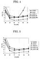
- the repeated recording properties at a recording linear velocity of 28m/s (8 double speeds) of obtained phase-change information recording medium were evaluated at each recording power of 28mW, 30mW, 32mW, 34mW, 36mW and 38mW.
- Example 16 The results of Example 16 are shown in Figure 4 and the results of Example 18 are shown in Figure 5.
- jitter was 9% or less for both Examples 16 and 18 at their most suitable powers.
- jitter of repeated recording at 1,000th time was 9% or less even at a power of as high as 36mW or more.
- the phase-change information recording medium according to the present invention is easy to perform initial crystallization, exhibits good recording sensitivity at a linear velocity as high as 10 double speeds or more with as much capacity as DVD-ROM, is capable of repeated recording and has excellent storage reliability. Therefore, it can be widely used in various phase-change information recording medium, in particular, optical recording medium of DVD system such as DVD-RAM, DVD-RW, DVD+RW, and the like.
Landscapes
- Chemical & Material Sciences (AREA)
- Engineering & Computer Science (AREA)
- Manufacturing & Machinery (AREA)
- Organic Chemistry (AREA)
- Materials Engineering (AREA)
- Mechanical Engineering (AREA)
- Metallurgy (AREA)
- Chemical Kinetics & Catalysis (AREA)
- Inorganic Chemistry (AREA)
- Physics & Mathematics (AREA)
- Optics & Photonics (AREA)
- Optical Record Carriers And Manufacture Thereof (AREA)
- Thermal Transfer Or Thermal Recording In General (AREA)
Abstract
Description
- The present invention relates to phase-change information recording medium (hereafter, may be referred to as "phase-change optical information recording medium", "optical recording medium", "optical information recording medium" or "information recording medium") which can perform at least one of recording, reproducing, erasing or rewriting of information by an optical change in the material forming a recording layer induced by laser beam irradiation, manufacturing method for the phase-change information recording medium, sputtering target, method for using the phase-change information recording medium and optical recording apparatus.
- Presently, a recording layer material of DVD (Digital Versatile Disk) system which can perform a speed recording at 2.5 double speeds (about 8.5m/s) has been developed and the demand for more high-speed recording is increasing. For this reason, materials for various phase-change recording layer are being investigated. For example, AgInSbTe material (
Patent Literature 1 for reference), GeGaSbTe material (Patent Literature 2 for reference), GeInSbTe material (Patent Literature 3 for reference), InSbSn material (Patent Literatures - Among these materials for phase-change recording layer used for DVD+RW(Digital Versatile Disc-Rewritable), there is a AgInSbTe material conventionally used for CD-RW which has been reformed to be capable of recording and erasing at high linear velocity. Since this AgInSbTe material corresponds to recording speed of high linear velocity region, a material in which the content of Sb is adjusted to be larger than that of recording material for CD-RW is being used. However, materials of high Sb composition ratio have a problem of lowering the crystallization temperature even though the crystallization speed increases. It is known that a decrease in crystallization temperature causes storage reliability deterioration. This problem of storage reliability of the phase-change information recording medium has been controlled by increasing Ag in the recording material of phase-change recording layer or by adding a quintessence such as Ge to keep it in an acceptable level from a practical standpoint up to 4-double speed DVD medium. However, an increase in the content of Sb for achieving higher linear velocity recording causes rapid decrease in crystallization temperature resulting in an extreme deterioration of amorphous mark stability. For this reason, it is assumed that the limit for making high-speed recording medium utilizing AgInSbTe material fit for practical use is as high as 4-double speed DVD.
- On the other hand, GaSb material for high-speed recording material of 4-double speed or more is being investigated. The GaSb material can perform a high-speed recording and at the same time, excels in storage reliability. However, GaSb material has low recording sensitivity because of high melting point of 600°C and has a drawback of requiring high power for high-speed recording. In addition, the crystallization speed must be accelerated by increasing the content of Sb in order to pursue a speeding up with GaSb material. However, when the content of Sb is 90 atomic percent or more, Sb becomes phase-separated and cannot pursue a uniform initial crystallization. If a uniform initial crystallization cannot be completed, initial recording property from the first recording to about 10 repeated recordings is notably deteriorated and cannot be put to practical use.
- Hence, a phase-change optical information recording medium which is easy to perform initial crystallization, exhibits good recording sensitivity at a linear velocity as high as 10 double speeds or more with as much capacity as DVD-ROM, is capable of repeated recording and has excellent storage reliability, and its associated technologies have not yet been provided, and their soon provision is desired under current circumstances.
[Patent Literature 1] Japanese Patent Application Laid-Open (JP-A) No. 2000-339751
[Patent Literature 2]JP-A No. 2002-225437
[Patent Literature 3]JP-A No. 2002-264515
[Patent Literature 4]JP-A No. 09-286174
[Patent Literature 5]JP-A No. 09-286175 - An object of the present invention is to provide a phase-change information recording medium which is easy to perform initial crystallization, exhibits good recording sensitivity at a linear velocity as high as 10 double speeds or more with as much capacity as DVD-ROM, is capable of repeated recording and has excellent storage reliability, and the sputtering target for manufacturing the phase-change information recording medium.
- When an information is recorded in the phase-change information recording medium by CAV (Constant Angular Velocity) recording system, because recording linear velocity differs depending on the radius location, a phase-change information recording medium of excellent repeated recording property in a broad area of recording linear velocity is required. Therefore, it is an object of the present invention to provide the phase-change information recording medium of excellent repeated recording property in a broad area of recording linear velocity with as much capacity as DVD-ROM, the sputtering target for manufacturing the phase-change information recording medium, the method for using the phase-change information recording medium and the optical recording apparatus.
- From a dedicated investigation that has been carried out to settle above issues, it is found that by utilizing alloys that consist mainly of Sn, Sb, Ga and Ge (90 atomic percent or more) as a material forming the phase-change recording layer, an appropriate sensitivity (with a melting point less than that of GaSb) can be obtained. For example, when a DVD recording system of 660nm wavelength and lens NA = 0.65 is used, it is found that satisfactory recording sensitivity, overwrite property and storage reliability can be obtained at a recording speed of about 35m/s or more and the phase-change information recording medium of excellent repeated recording property in a broad area of recording linear velocity with as much capacity as DVD-ROM can be provided.
- The present invention is based on the knowledge of the present inventor and the measures to solve above-mentioned problems are the following.
- <1> The phase-change information recording medium comprising a substrate and at least a first protective layer, a phase-change recording layer, a second protective layer, and a reflective layer disposed on the substrate in one of this sequence and reverse sequence, wherein the phase-change recording layer comprises a composition expressed in following
Formula 1. Because the phase-change recording layer of the phase-change information recording medium comprises the composition expressed by Formula 1, obtaining the phase-change information recording medium of excellent storage stability which is capable of repeated recording at a recording linear velocity of 3 double speeds or more of DVD with as much capacity as DVD-ROM is possible.
Inabove Formula 1, X represents at least one element selected from Ag, Zn, In and Cu. α, β, γ, δ, ε and ζ represent composition ratio (atomic percent) of each element and are expressed as follows:
- <2> The phase-change information recording medium defined in <1>, wherein the phase-change recording layer comprises a composition expressed by following
Formula 1. Because the phase-change recording layer of the phase-change information recording medium comprises the composition expressed by Formula 1, obtaining the phase-change information recording medium capable of appropriate repeated recording at a recording linear velocity of 10 double speeds or more of DVD with as much capacity as DVD-ROM is possible.
Inabove Formula 1, X represents at least one element selected from Ag, Zn, In and Cu. α, β, γ, δ, ε and ζ represent composition ratio (atomic percent) of each element and are expressed as follows:
- <3> The phase-change information recording medium defined in <2>, wherein the phase-change recording layer comprises the composition expressed by following
Formula 1. Because the phase-change recording layer of the phase-change information recording medium defined in <3> comprises the composition expressed by Formula 1, obtaining the information recording medium capable of appropriate repeated recording at a recording linear velocity of 3 double speeds to 8 double speeds of DVD is possible. Furthermore, because repeated recording in a broad area of recording linear velocity is good, it is possible to record the information in the phase-change information recording medium by CAV (Constant Angular Velocity) of which the recording linear velocity differs depending on the radius location.
Inabove Formula 1, X represents at least one element selected from Ag, Zn, In and Cu. α, β, γ, δ, ε and ζ represent composition ratio (atomic percent) of each element and are expressed as follows:
- <4> The phase-change information recording medium defined in one of <1> to <3>, wherein the phase-change recording layer comprises the composition expressed by following
Formula 2.
Inabove Formula 2, α, β, γ and δ represent composition ratio (atomic percent) of each element and are expressed as follows:
- <5> The phase-change information recording medium defined in <4>, wherein the phase-change recording layer comprises the composition expressed by following
Formula 2.
Inabove Formula 2, α, β, γ and δ represent composition ratio (atomic percent) of each element and are expressed as follows:
- <6> The phase-change information recording medium defined in <5>, wherein the phase-change recording layer comprises the composition expressed by following
Formula 2.
Inabove Formula 2, α, β, γ and δ represent composition ratio (atomic percent) of each element and are expressed as follows:
- <7> The phase-change information recording medium defined in one of <1> to <6>, wherein the phase-change recording layer performs at least one of recording, reproducing, erasing and rewriting of information through reversible phase-change induced by laser beam irradiation.
- <8> The phase-change information recording medium defined in <7>, wherein when the thickness of the first protective layer being t1 (nm), the thickness of the phase-change recording layer being t2 (nm), the thickness of the second protective layer being t3 (nm), the thickness of the reflective layer being t4 (nm), and the wavelength of the laser beam being λ (nm), the relations of the following formulas, 0.070 ≤ t1 / λ ≤ 0.160, 0.015 ≤ t2 / λ ≤ 0.032, 0.005 ≤ t3 / λ ≤ 0.040, and 0.100 ≤ t4 / λ are satisfied. An appropriate thickness range of the first protective layer, the phase-change recording layer, the second protective layer and the reflective layer of the phase-change information recording medium defined in <8> can be regulated with a relation to laser wavelength λ (nm) and if the laser light wavelength used for the record reproduction of the phase-change information recording medium is decided, an appropriate thickness range may be selected following these Formulas and designing a medium is possible.
- <9> The phase-change information recording medium defined in one of <1> to <8>, wherein the first protective layer and the second protective layer comprise a mixture of ZnS and SiO2.
- <10> The phase-change information recording medium defined in <1> to <9>, wherein the reflective layer comprises one of Ag and Ag alloy.
- <11> The phase-change information recording medium defined in <1> to <10>, wherein an interface layer is disposed between the phase-change recording layer and the first protective layer.
- <12> The phase-change information recording medium defined in <11>, wherein the interface layer comprises SiO2 and the thickness of the interface layer is 2nm to 10nm.
- <13> The phase-change information recording medium defined in <1> to <12>, wherein the third protective layer is disposed between the second protective layer and the reflective layer.
- <14> A sputtering target comprising a composition expressed by following
Formula 1, wherein the sputtering target is used for manufacturing the phase-change recording layer.
Inabove Formula 1, X represents at least one element selected from Ag, Zn, In and Cu. α, β, γ, δ, ε and ζ represent composition ratio (atomic percent) of each element and are expressed as follows:
- <15> The sputtering target defined in <14>, wherein the composition is expressed by following
Formula 1.
Inabove Formula 1, X represents at least one element selected from Ag, Zn, In and Cu. α, β, γ, δ, ε and ζ represent composition ratio (atomic percent) of each element and are expressed as follows:
- <16> The sputtering target defined in <15>, wherein the composition is expressed by following
Formula 1.
Inabove Formula 1, X represents at least one element selected from Ag, Zn, In and Cu. α, β, γ, δ, ε and ζ represent composition ratio (atomic percent) of each element and are expressed as follows:
- <17> The sputtering target defined in one of <14> to <16>, wherein the composition is expressed by following
Formula 2 and the sputtering target is used for manufacturing the phase-change recording layer.
Inabove Formula 2, α, β, γ and δ represent composition ratio (atomic percent) of each element and are expressed as follows:
- <18> The sputtering target defined in <17>, wherein the composition is expressed by following
Formula 2.
Inabove Formula 2, α, β, γ and δ represent composition ratio (atomic percent) of each element and are expressed as follows:
- <19> The sputtering target defined in <18>, wherein the composition is expressed by following
Formula 2.
Inabove Formula 2, α, β, γ and δ represent composition ratio (atomic percent) of each element and are expressed as follows:
- <20> A manufacturing method for the phase-change recording medium comprising phase-change recording layer forming to form the phase-change recording layer by sputtering using the sputtering target defined in one of <14> to <19>, wherein the phase-change information recording medium comprises at least a first protective layer, a phase-change recording layer, a second protective layer and a reflective layer disposed on the substrate in one of this sequence and reverse sequence.
- <21> The manufacturing method for the phase-change information recording medium defined in <20> comprising initial crystallization, wherein the phase-change information recording medium is rotated at a certain linear velocity within a range of 10m/s to 21m/s and the initial crystallization is performed at a power density of 15mW/µm2 to 40mW/µm2.
- <22> A method for using the phase-change information recording medium wherein at least one of recording, reproducing, erasing and rewriting of information is performed by laser beam irradiation from the first protective layer side of the phase-change information recording medium defined in one of <1> to <13>.
- <23> An optical recording apparatus wherein at least one of recording, reproducing, erasing and rewriting of information is performed by laser beam irradiation from a laser beam source to the phase-change information recording medium and the phase-change information recording medium is the phase-change information recording medium defined in one of <1> to <13>.
- In the method for using the phase-change information recording medium, at least one of recording; reproducing, erasing and rewriting of information is performed by laser beam irradiation to the phase-change information recording medium. As a result, one of recording, reproducing, erasing and rewriting of information can be effectively performed safely with certainty.
- In the optical recording apparatus according to the present invention wherein at least one of recording, reproducing, erasing and rewriting of information is performed by laser beam irradiation from a laser beam source to the phase-change information recording medium and above-mentioned phase-change information recording medium is the phase-change information recording medium according to the present invention. In the optical recording apparatus according to the present invention, at least one of recording, reproducing, erasing and rewriting of information can be performed safely with certainty.
-
- FIG. 1 is a cross-sectional view showing an exemplary phase-change information recording medium of the invention.
- FIG. 2 is a graph showing the jitter from the first time to 1,000th time of repeated recording of the phase-change information recording medium of Example 16.
- FIG. 3 is a graph showing the jitter from the first time to 1,000th time of repeated recording of the phase-change information recording medium of Example 17.
- FIG. 4 is a graph showing the repeated recording property of the phase-change information recording medium of Example 16.
- FIG. 5 is a graph showing the repeated recording property of the phase-change information recording medium of Example 18.
- The phase-change information recording medium of the invention comprises a substrate and at least a first protective layer, a phase-change recording layer, a second protective layer and a reflective layer disposed on the substrate in one of this sequence and reverse sequence and other layers as necessary. In the present case, at least one of recording, reproducing, erasing and rewriting of information is performed by a laser beam irradiated from the first protective layer side of the phase-change information recording medium.
- In order to achieve excellent storage stability and repeated recording at 3 double speeds or more of DVD with as much capacity as DVD-ROM, the phase-change recording layer is required to have the composition expressed by
Formula 1.
- In
above Formula 1, X represents at least one element selected from Ag, Zn, In and Cu. α, β, γ, δ, ε and ζ represent composition ratio (atomic percent) of each element and are expressed as follows:
- In the present case, the phase-change recording layer comprising the composition expressed by
Formula 2 is especially preferable.
- In
above Formula 2, α, β, γ and δ represent composition ratio (atomic percent) of each element and are expressed as follows:
- Because melting point of Sn50Sb50 compound is as low as 425°C and the speed of crystallization is rapid, there is a potential in materializing a high-speed recording medium of good recording sensitivity. However, the speed of crystallization of Sn50Sb50 compound is so rapid that it can be crystallized at a room temperature and there is no way to make it amorphous with current evaluation apparatus for DVD+RW, therefore Sn50Sb50 compound alone cannot be used as a phase-change recording layer of DVD+RW. A material capable of repeated recording with excellent storage stability was searched by improving the composition having Sn50Sb50 compound as a parent phase. As a result, it was found that an optical recording medium capable of repeated recording with excellent storage stability can be provided by simultaneously adding Ga by which Sn50Sb50 compound can easily be crystallized and made amorphous, and Ge having advantageous effect over storage stability. When only Ga is added, a decrease in the reflectance ratio of crystal phase occurs after long-term storage and the shelf property (record reproduction property after being left unattended for extended time), one of the evaluation item for storage stability, is deteriorated. On the other hand, when only Ge is added, length of amorphous mark is fluctuated and jitter property is not improved.
- Moreover, because Ga and Ge have an affect of making crystallization speed of Sn50Sb50 compound slow, crystallization speed may be altered by controlling Ga + Ge atomic percent. For example, when Ga + Ge is 20 atomic percent or more, recording property at slow speed is especially favorable and at the same time, when Ga + Ge is 10 atomic percent to 15 atomic percent, high-speed recording property at 8 double speeds or more is especially favorable.
- In consequence, the phase-change recording layer comprises the composition expressed by following
Formula 1. This makes it possible to obtain the phase-change information recording medium of excellent storage stability which is capable of repeated recording at a recording linear velocity of 3 double speeds or more of DVD with as much capacity as DVD-ROM.
- In
above Formula 1, X represents at least one element selected from Ag, Zn, In and Cu. α, β, γ, δ, ε and ζ represent composition ratio (atomic percent) of each element and are expressed as follows:
- In the present case, α, β, γ, δ, ε and ζ are preferably 5 ≤ α ≤ 20, 40 ≤ β ≤ 85, 5 ≤ γ ≤ 20, 5 ≤ δ ≤ 20, 0 ≤ ε ≤ 7, 0 ≤ ζ ≤ 7 and more preferably α + β + γ + δ + ε + ζ = 100.
- α, β, γ, δ, ε and ζ are preferably 10 ≤ α ≤ 20, 50 ≤ β ≤ 80, 5 ≤ γ ≤ 15, 5 ≤ δ ≤15, 0 ≤ ε ≤7, 0 ≤ ζ ≤ 7 and more preferably α + β + γ + δ + ε + ζ = 100.
- The phase-change recording layer, in specific, is preferably of the composition expressed by following
Formula 2.
- In
above Formula 2, α, β, γ and δ represent composition ratio (atomic percent) of each element and are expressed as follows:
- In the present case, α, β, γ and δ are preferably 5 ≤ α ≤ 20, 40 ≤ β ≤ 85, 5 ≤ γ ≤ 20, 5 ≤ δ ≤ 20 and α + β + γ + δ = 100.
- α, β, γ and δ are more preferably 10 ≤ α ≤ 20, 50 ≤ β ≤ 80, 5 ≤ γ ≤ 15, 5 ≤ δ ≤ 15 and α + β + γ + δ = 100.
- In the composition expressed by
Formulas - It is favorable to add at least one element selected from Ag, Zn, In and Cu to the phase-change recording layer. This improves storage reliability. The content of these elements is preferably 0 atomic percent to 10 atomic percent and more preferably 0 atomic percent to 7 atomic percent. When the content is more than 10 atomic percent, crystallization temperature becomes excessively high and initial crystallization may become difficult.
- Furthermore, it is favorable to add Te to the phase-change recording layer. The content of Te is preferably 0 atomic percent to 10 atomic percent and more preferably 0 atomic percent to 7 atomic percent. This makes initial crystallization easy and a uniform crystal condition become easily obtainable and an increase of jitter from the first time to about 10th time of repeated recording can be lowered.
- In the invention, when the thickness of the first protective layer being t1 (nm), the thickness of the phase-change recording layer being t2 (nm), the thickness of the second protective layer being t3 (nm), the thickness of the reflective layer being t4 (nm), and the wavelength of the laser beam being λ (nm), it is preferable that the relations of the following formulas, 0.070 ≤ t1 / λ ≤ 0.160, 0.015 ≤ t2 / λ ≤ 0.032, 0.005 ≤ t3 / λ ≤ 0.040, and 0.100 ≤ t4 / λ are satisfied.
- For example, in order to maintain DVD-ROM reproduction compatibility, the reflectance ratio of optical recording medium of DVD system with a wavelength of 630nm to 680 nm should be 18% or more. To satisfy this optical assumption, the thickness of the phase-change recording layer and the first protective layer are mainly controlled while the thickness of the second protective layer and the reflective layer are adjusted to be within a range that satisfies above thickness condition. If the thickness of the phase-change recording layer is too thin, light absorbing power of the recording layer may be deteriorated. If the thickness is too thick, recording sensitivity may be deteriorated. Consequently, the thickness of the phase-change recording layer is preferably in a range of 0.015 ≤ t2 / λ ≤ 0.032.
- When the thickness of the phase-change recording layer is set within the range of 0.015 ≤ t2 / λ ≤ 0.032, the second thickness range and the third thickness range having more thickness exist other than the first thickness range of 0.070 ≤ t1 / λ ≤ 0.160 as the thickness condition of the first protective layer satisfying above optical condition. But the second and third thickness range is thicker than the first thickness range and takes more manufacturing time per film; the first thickness range is favorable in materializing a low-cost disc from the manufacturing view point of the phase-change information recording medium. Consequently, thickness of the first protective layer preferably satisfies the relation of the Formula 0.070 ≤ t1 / λ ≤ 0.160 when the wavelength of the laser beam being λ.
- The second protective layer temporally reserves heat generated by thermal relaxation of light energy absorbed within the phase-change information recording medium (the main body of the absorption is the material of phase-change recording layer), propagates it to the reflective layer and releases. Therefore, it is preferable that the second protective layer is not too much thick, and is preferably within a range of 0.005 ≤ t3 / λ ≤ 0.040. If the thickness of the second protective layer is thicker than above-mentioned, a recording mark blurs due to gathered heat in the phase-change recording layer, and the recording properties, particularly jitter property is deteriorated. The jitter property is evaluated by a variation in mark edge expressed based on the channel cycle (Tw), σ/Tw. On the other hand, if the thickness of the second protective layer is thinner than above-mentioned, a problem arises in that satisfactory recording properties cannot be obtained, because absorbed light energy within the phase-change recording layer is released to the reflective layer before reaching the amount capable of exhibiting the principle of phase-change recording, in which light energy absorbed in the phase-change recording layer is accumulated to dissolve the phase-change recording layer, thereby making a record mark.
- Because power density of laser beam varies depending on the wavelength used in the recording system, it is required to change the thickness of above-mentioned second protective layer, however, this can be resolved by setting the thickness of the second protective layer within the range that satisfies above-mentioned optical thickness condition. This also applies to the thickness condition of other layers mentioned above.
- Next, an exemplary layer structure of the phase-change information recording medium according to the present invention will be described in detail based on the accompanying drawing.
- Here, Figure 1 is a cross-sectional schematic view showing an exemplary phase-change information recording medium according to the present invention, in which a
substrate 1, a firstprotective layer 2, a phase-change recording layer 3, a secondprotective layer 4, a thirdprotective layer 5 and areflective layer 6 are laminated on asubstrate 1 in the named order. In addition, it is preferable to dispose an interface layer between the phase-change recording layer 3 and the firstprotective layer 2, although not shown in the drawings. Furthermore, it is also favorable to form a protective layer made of ultraviolet curing resin on the reflective layer by spin coat and other substrates may be bonded on the protective layer as necessary for further reinforcement or protection of the phase-change information recording medium. - Generally, glass, ceramics, resin, and the like are used for the material of the
substrate 1 and the substrate made from resin is preferable in terms of formability and cost. Examples of resin include polycarbonate resin, acrylate resin, epoxy resin, polystyrene resin, acrylonitrile-styrene copolymer, polyethylene resin, polypropylene resin, silicone resin, fluorine resin, ABS resin, urethane resin, and the like. Of these, polycarbonate resin and acrylate resin are especially preferable in terms of formability, optical properties and cost. - The thickness of
substrate 1 is not particularly limited and the thickness is determined by wavelength of the laser or focusing property of the pickup lens generally used. The substrate having a thickness of 1.2mm is used for CD of 780nm wavelength and a substrate having a thickness of 0.6 mm is used for DVD of 650nm to 665nm wavelength. - A substrate of polycarbonate resin having a race for tracking on its surface, is in a form of a disc of 12cm diameter and 0.6mm thickness and having excellent workability and optical property is favorable, for example. The race for tracking is preferably a meandering race within a range of 0.74 ± 0.03µm pitch, 22nm to 40nm depth and 0.2µm to 0.4µm width. In particular, by making the race deep, reflectance ratio of the phase-change information recording medium decreases and the modulation depth becomes large.
- In addition, an adhesive layer for bonding the
substrate 1 where information signal is written in and the bonding substrate is formed of double-sided adhesive sheet of which binder is coated on both sides of the base film, thermo-curing resin or ultraviolet curing resin. The thickness of the adhesive layer is generally about 50µm. - The bonding substrate (dummy substrate) is not necessary transparent when the adhesive layer is an adhesive sheet or thermo-curing resin, however, when the adhesive layer is an ultraviolet curing resin, it is favorable to use a transparent substrate through which ultraviolet ray is transmitted. In general, the thickness of the bonding substrate is preferably 0.6mm, as same as the
transparent substrate 1 in which information signal is written in. - The first
protective layer 2 is preferably having good adhesiveness with the substrate and the phase-change recording layer, is highly thermostable, and is also preferably having optical properties suitable for repeated recording at a high linear velocity because it also serves as an optical interference layer which makes an effective light absorption of the phase-change recording layer possible. - Examples of the material for the first protective layer include metal oxides such as SiO, SiO2, ZnO, SnO2, Al2O3, TiO2, In2O3, MgO, ZrO2; nitrides such as Si3N4, AlN, TiN, BN, ZrN; sulfides such as ZnS, In2S3, TaS4; carbides such as SiC, TaC, B4C, WC, TiC, ZrC; diamond-like carbon or mixtures thereof. Of these, the mixture of ZnS and SiO2 is preferable. The mixture molar ratio (ZnS:SiO2) is preferably 50 to 90 : 50 to 10 and more preferably 60 to 90 : 40 to 10.
- Examples of the method for forming the first
protective layer 2 include various vapor-phase growths such as vacuum evaporation method, sputtering method, plasma CVD method, optical CVD method, ion plating method and electron-beam deposition method. Among these, the sputtering method excels in mass productivity, layer quality, and the like. For example, the following sputtering condition is favorable: Ar gas as a film-forming gas, electricity input of 3kW and Ar gas pressure of 2 × 10⁻³ Torr (air pressure of film-forming chamber) - The thickness of the first protective layer (t1) is preferably 50nm to 90nm and satisfying the formula, 0.070 ≤ t1 / λ ≤ 0.160 when the wavelength of laser beam is regarded as λ. When it is thinner than this range, it does not function as a heat-resistant protective layer and when it is thicker, interfacial peeling is likely to occur.
- The phase-
change recording layer 3 is preferably having a composition expressed byFormulas - The thickness of the phase-change recording layer (t2) is preferably satisfying the formula, 0.015 ≤ t2 / λ ≤ 0.032 as mentioned above, when the wavelength of laser beam is regarded as λ. When the thickness of the phase-change recording layer is thinner than this range, light absorbing power decreases and it may not function as a phase-change recording layer and when it is thicker, recording sensitivity may be deteriorated.
- Examples of the method for forming the phase-change recording layer include various vapor-phase growths such as vacuum evaporation method, sputtering method, plasma CVD method, optical CVD method, ion plating method and electron-beam deposition method Among these, the sputtering method excels in mass productivity, layer quality, and the like. For example, the following sputtering condition i favorable: Ar gas as a film-forming gas, electricity input of 1kW and Ar gas pressure of 2 × 10⁻³ Torr (air pressure of film-forming chamber)
- The second
protective layer 4 is preferably having good adhesiveness with the substrate and the phase-change recording layer, is highly thermostable and having optical properties suitable for repeated recording at a high linear velocity because it also serves as an optical interference layer which makes an effective light absorption of the phase-change recording layer possible. - Examples of the material for the second protective layer include metal oxides such as SiO, SiO2, ZnO, SnO2, Al2O3, TiO2, In2O3, MgO, ZrO2; nitrides such as Si3N4, AlN, TiN, BN, ZrN; sulfides such as ZnS, In2S3, TaS4; carbides such as SiC, TaC, B4C, WC, TiC, ZrC; diamond-like carbon or mixtures thereof. Of these, the mixture of ZnS and SiO2 is preferable. The mixture molar ratio (ZnS:SiO2) is preferably 50 to 90 : 50 to 10 and more preferably 60 to 90 : 40 to 10.
- Examples of the method for forming the second protective layer include various vapor-phase growths such as vacuum evaporation method, sputtering method, plasma CVD method, optical CVD method, ion plating method and electron-beam deposition method. Among these, the sputtering method excels in mass productivity, layer quality, and the like. For example, the following sputtering condition is favorable: Ar gas as a film-forming gas, electricity input of 3kW and Ar gas pressure of 2 × 10⁻³ Torr (air pressure of film-forming chamber).
- The thickness of the second protective layer (t3) is preferably 6nm to 20nm and satisfying the formula, 0.005 ≤ t3 / λ ≤ 0.040 when the wavelength of laser beam is regarded as λ as mentioned above. When the thickness of the second protective layer is thinner than this range, recording sensitivity may be deteriorated and when it is thicker, too much heat may be gathered inside.
- The reflective layer serves as an optical reflective layer while it also serves as a heat dissipation layer for dissipating heat added to the phase-change recording layer by irradiating laser beam at the time of recording. Choosing a reflective layer is quite important in a phase-change information recording medium corresponding to high linear velocity, because an amorphous mark forming is heavily affected by cooling rate through heat dissipation.
- For the
reflective layer 6, a metallic material, for example, Al, Au, Ag, Cu, Ta, and the like or metal alloys thereof can be used. Further, as an element to be added to these metallic materials, Cr, Ti, Si, Cu, Ag, Pd, Ta or the like can be used. Among these materials, it is preferred that one of Ag and Ag metal alloy is contained therein. This is because a metal with high thermal conductivity and high reflectance is usually desirable for the reflective layer constituting the phase-change information recording medium in terms of thermal conductivity for modulating cooling rate against the heat generated at the time of recording and also in terms of an optical viewpoint of improving the contrast of reproduction signals by utilizing interference effect, and pure Ag or an Ag metal alloy respectively has extremely high thermal conductivity of 427W/m · K, and a quenching configuration suitable for forming an amorphous mark can be realized immediately after the phase-change recording layer reaches a high temperature at the time of recording. - Pure silver is the most suitable in consideration of its high thermal conductivity, but Cu may be added in consideration of corrosion resistance. In this case, in order not to impair the property of Ag, the range of the copper addition amount is preferably from about 0.1 atomic percent to about 10 atomic percent, and more preferably within the range of 0.5 atomic percent to 3 atomic percent. An excessive addition of copper may deteriorate high heat conductivity of Ag.
- Examples of the method for forming the
reflective layer 6 include various vapor-phase growths such as vacuum evaporation method, sputtering method, plasma CVD method, optical CVD method, ion plating method and electron-beam deposition method. Among these, the sputtering method excels in mass productivity, layer quality, and the like. For example, the following sputtering condition is favorable: Ar gas as a film-forming gas, electricity input of 5kW and Ar gas pressure of 2 × 10⁻³ Torr (air pressure of film-forming chamber). - The heat dissipation ability of the reflective layer is basically proportional to the thickness of the layer; however, excellent disc properties are available, if the thickness of the reflective layer is 60nm or more. In this case, there is no particular maximum limit value thereof, and a thickness within an allowable range from disc manufacturing cost perspective may be used, however, about 300nm or less is preferable and it is preferable that the thickness of the reflective layer (t4), as described above, satisfies the formula, 0.100 ≤ t4 / λ, when the wavelength of laser beam is regarded as λ. When the thickness of the reflective layer is thinner than this range, heat dissipation effect may not be obtained.
- It is noted that a resin protective layer may be disposed on the
reflective layer 6 as necessary. This resin protective layer has an effect for protecting phase-change recording layer in the process flow when manufactured as a product and it is usually formed through the use of an ultraviolet-curing resin. The thickness of the resin protective layer is preferably within the range of 2µm to 5µm. - It is preferred that the third
protective layer 5 is disposed between the secondprotective layer 4 and thereflective layer 6. - Examples of material for the third
protective layer 5 include Si, SiC, SiN, SiO2, TiC, TiO2, TiC-TiO2, NbC, NbO2, NbV-NbO2, Ta2O5, Al2O3, ITO, GeN, ZrO2, and the like. Among them, TiC-TiO2, Si or SiC is particularly preferable in terms of high-barrier properties. - If a protective layer comprising sulfur such as a mixture of ZnS and SiO2 is used, and when pure Ag or Ag alloy is used for a reflective layer, sulfur will diffuse toward Ag and causes a problem of disc defect (Ag reaction to sulfur). Thus, for the third protective layer for preventing such reaction, it is desirable to select a proper material from the following perspective:
- (1) having barrier properties to prevent Ag from reacting to sulfur; (2) being optically transparent to laser beam; (3) having low-thermal conductivity for forming an amorphous mark; (4) having good adhesion to protective layers and reflective layers; and (5) being easy to form. A material mainly made of TiC-TiO2, Si or SiC that satisfies above conditions is suitable for constituent material of the third protective layer.
- The thickness of the third protective layer is preferably 2nm to 20nm, and more preferably 2nm to 10nm. If the thickness is less than 2nm, the third protective layer may not function as a barrier layer, and if the thickness is more than 20nm, the modulation degree may be decreased.
- It is preferred that an interface layer is disposed between the first
protective layer 2 and the phase-change recording layer 3. The interface layer is preferably containing SiO2 and having thickness of 2nm to 10nm. This decreases damages of which the substrate receives when recording at high power and gives advantageous effect over repeated recording property at high power recording; therefore having a wide margin of recording power is possible. If the thickness of the interface layer is less than 2nm, forming a uniform SiO2 film may be difficult, and if the thickness is more than 10nm, film separation may become more likely to occur. - The phase-change information recording medium according to the present invention has been described in detail; however, the present invention is not limited to the disclosed aspects and various modifications without departing from the scope of the present invention are acceptable. For example, the present invention may be applied to a phase-change information recording medium in which the same or different types of two phase-change information recording media are bonded together through a resin protective layer instead of a bonding substrate as seen in DVD system.
- The sputtering target according to the present invention has a composition expressed by following
Formula 1 and is used for manufacturing the phase-change recording layer.
- In
above Formula 1, X represents at least one element selected from Ag, Zn, In and Cu. α, β, γ, δ, ε and ζ represent composition ratio (atomic percent) of each element and are expressed as follows:
- In the present case, α, β, γ, δ, ε and ζ are preferably 5 ≤ α ≤ 20, 40 ≤ β ≤ 85, 5 ≤ γ ≤ 20, 5 ≤ δ ≤ 20, 0 ≤ ε ≤ 7, 0 ≤ ζ ≤7 and α + β + γ + δ + ε + ζ = 100.
- α, β, γ, δ, ε and ζ are more preferably 10 ≤ α ≤ 20, 50 ≤ β ≤ 80, 5 ≤ γ ≤ 15, 5 ≤ δ ≤ 15, 0 ≤ ε ≤ 7, 0 ≤ ζ ≤ 7 and α + β + γ + δ + ε + ζ = 100.
- The sputtering target is preferably having a composition expressed by following
Formula 2 and is used for manufacturing the phase-change recording layer.
- In
above Formula 2, α, β, γ and δ represent composition ratio (atomic percent) of each element and are expressed as follows:
- In the present case, α, β, γ and δ are preferably 5 ≤ α ≤ 20, 40 ≤ β ≤ 85, 5 ≤ γ ≤ 20, 5 ≤ δ ≤ 20 and α + β + γ + δ = 100.
- α, β, γ and δ are more preferably 10 ≤ α ≤ 20, 50 ≤ β ≤ 80, 5 ≤ γ ≤ 15, 5 ≤ δ ≤ 5 and α + β + γ + δ = 100.
- The manufacturing method for sputtering target is not particularly limited and may be selected accordingly and a certain prearranged amount is weighed and heat melted in a glass ampoule. And then it is crushed in a mill and obtained powder is heat sintered to manufacture a discoid sputtering target.
- By the present invention, a phase-change information recording medium which is easy to perform initial crystallization, exhibits good recording sensitivity at a linear velocity as high as 10 double speeds or more with as much capacity as DVD-ROM, is capable of repeated recording and has good storage reliability, can be provided.
- Furthermore, the phase-change information recording medium of good repeated recording property in a broad area of recording linear velocity with as much capacity as DVD-ROM and the sputtering target for manufacturing the phase-change information recording medium can be provided.
- The manufacturing method for the phase-change recording medium of the invention includes at least phase-change recording layer forming, initial crystallization and other steps as necessary.
- The phase-change recording layer forming is a step to form a phase-change recording layer by sputtering using the sputtering target of the invention.
- The sputtering is not particularly limited and may be selected from known sputtering accordingly, for example, the sputtering using Ar gas as a film-forming gas, electricity input of 1kW to 5kW and gas flow rate of 10sccm to 40sccm is favorable. The Ar gas pressure inside the chamber during sputtering is preferably 7.0 × 10⁻³mTorr (mbar) or less.
- The initial crystallization is a step to perform an initial crystallization at a power density of 15mW/µm to 40mW/µm while rotating the phase-change information recording medium at a certain velocity within a range of 10m/s to 21m/s.
- Specifically the initial crystallization is performed by irradiating the light for recording such as laser diode (with an emission wavelength of 600nm to 720nm, for example) from the substrate side via objective lens while rotating the phase-change information recording medium at a certain linear velocity or constant angular velocity. The temperature of the phase-change recording layer increases locally as it absorbs irradiated light and information is recorded by generating a pit and modifying its optical property, for example. The reproduction of above-mentioned recorded information can be done by irradiating a laser beam from the first protective layer side while rotating the phase-change information recording medium at a certain linear velocity and detecting the reflected light.
- The method for using the phase-change information recording medium of the invention wherein at least one of recording, reproducing, erasing and rewriting of information is performed by laser beam irradiation from the first protective layer side of the phase-change information recording medium of the invention.
- In the present case, the wavelength of laser beam is preferably 400nm to 780nm and more preferably 630nm to 680nm.
- The optical recording apparatus of the invention performs information recording in a phase-change information recording medium by irradiating laser beam from laser beam source to the phase-change information recording medium and the phase-change information recording medium is the phase-change information recording medium of the invention.
- The optical recording apparatus is not limited and may be selected accordingly and the example of such apparatus comprises a laser beam source of laser diode, and the like which emits laser beams; a focusing lens which focuses the laser beam emitted from the laser beam source to the optical recording medium mounted on a spindle; optical elements which guides laser beam emitted from the laser beam source to both of the focusing lens and a laser beam detector; the laser beam detector for detecting the reflected light of the laser beam, and other units as necessary.
- The optical recording apparatus guides laser beam emitted from the laser beam source to the focusing lens through optical elements to perform recording in a phase-change information recording medium by concentrating and irradiating the laser beam through focusing lens to the phase-change information recording medium. Here, the optical recording apparatus guides the reflected beam of the laser beam to the laser beam detector to control the amount of beam of the laser beam source based on the amount of laser beam detected by the laser beam detector.
- The laser beam detector converts the detected amount of laser beam into power voltage or power current and outputs them as a signal of the detected amount.
- Examples of other units include controlling unit. The controlling unit is not particularly limited as long as it is able to control movements of the individual units, and may be selected accordingly and examples of controlling unit include sequencer for irradiating and scanning intensely modulated laser beam; equipment such as computer devices, and the like.
- Herein below, the invention is explained in detail with referring to Examples; however, Examples should not be construed as limiting the scope of the invention.
- A phase-change information recording medium (disc) was prepared as follow. Sputtering was conducted using a sheet sputtering apparatus (Big Sprinter by Unaxis Incorporated) under Ar gas atmosphere with electricity input of 1kW to 5kW and Ar gas pressure of 2 × 10⁻³ Torr.
- A polycarbonate resin substrate of 0.74µm track pitch, 27nm groove depth, 12cm diameter and 0.6mm thickness was provided.
- First, using a sputtering target of (ZnS)80 (SiO2)20 composition (mole percent), a first protective layer of 80nm thickness was formed on the substrate by sputtering.
- Next, using a sputtering target of Sn5Sb75Ga13Ge7 composition (atomic percent), a phase-change recording layer of 20nm thickness was formed on the first protective layer by sputtering.
- Next, using the sputtering target of (ZnS)80 (SiO2)20 composition (mole percent), a second protective layer of 14nm thickness was formed on the phase-change recording layer by sputtering.
- Next, using a sputtering target of SiC, a third protective layer of 4nm thickness was formed on the second protective layer by sputtering.
- Next, using a sputtering target of Ag, a reflective layer of 180nm thickness was formed on the third protective layer by sputtering.
- Next, an organic protective layer was formed by coating acrylic curing resin of 5µm to 10µm thickness on the reflective layer using a spinner and performing ultraviolet-curing afterward.
- Finally, a polycarbonate resin substrate of 12cm diameter and 0.6mm thickness was bonded to the organic protective layer using an adhesive. With these procedures, the phase-change information recording medium of Example 1 was prepared.
- The phase-change information recording medium of Example 2 was prepared similarly to Example 1, except for forming a phase-change recording layer by sputtering using a sputtering target of Sn25Sb56Ga9Ge10 composition (atomic percent).
- The phase-change information recording medium of Example 3 was prepared similarly to Example 1, except for forming a phase-change recording layer by sputtering using a sputtering target of Sn24Sb41Ga18Ge17 composition (atomic percent).
- The phase-change information recording medium of Example 4 was prepared similarly to Example 1, except for forming a phase-change recording layer by sputtering using a sputtering target of Sn10Sb78Ga8Ge4 composition (atomic percent).
- The phase-change information recording medium of Example 5 was prepared similarly to Example 1, except for forming a phase-change recording layer by sputtering using a sputtering target of Sn19Sb67Ga2Ge12 composition (atomic percent).
- The phase-change information recording medium of Example 6 was prepared similarly to Example 1, except for forming a phase-change recording layer by sputtering using a sputtering target of Sn22Sb55Ga18Ge5 composition (atomic percent).
- The phase-change information recording medium of Example 7 was prepared similarly to Example 1, except for forming a phase-change recording layer by sputtering using a sputtering target of Sn16Sb72Ga10Ge2 composition (atomic percent).
- The phase-change information recording medium of Example 8 was prepared similarly to Example 1, except for forming a phase-change recording layer by sputtering using a sputtering target of Sn22Sb55Ga4Ge19 composition (atomic percent).
- The phase-change information recording medium of Comparative Example 1 was prepared similarly to Example 1, except for forming a phase-change recording layer by sputtering using a sputtering target of Sn3Sb60Ga18Ge19 composition (atomic percent).
- The phase-change information recording medium of Comparative Example 2 was prepared similarly to Example 1, except for forming a phase-change recording layer by sputtering using a sputtering target of Sn27Sb67Ga4Ge2 composition (atomic percent).
- The phase-change information recording medium of Comparative Example 3 was prepared similarly to Example 1, except for forming a phase-change recording layer by sputtering using a sputtering target of Sn24Sb39Ga18Ge19 composition (atomic percent).
- The phase-change information recording medium of Comparative Example 4 was prepared similarly to Example 1, except for forming a phase-change recording layer by sputtering using a sputtering target of Sn20Sb66Ga1Ge13 composition (atomic percent).
- The phase-change information recording medium of Comparative Example 5 was prepared similarly to Example 1, except for forming a phase-change recording layer by sputtering using a sputtering target of Sn13Sb52Ga21Ge14 composition (atomic percent).
- The phase-change information recording medium of Comparative Example 6 was prepared similarly to Example 1, except for forming a phase-change recording layer by sputtering using a sputtering target of Sn18Sb61Ga20Ge1 composition (atomic percent).
- The phase-change information recording medium of Comparative Example 7 was prepared similarly to Example 1, except for forming a phase-change recording layer by sputtering using a sputtering target of Sn15Sb61Ga3Ge21 composition (atomic percent).
- Initial crystallization of each obtained phase-change information recording medium was performed using laser diode of 810nm wavelength. In particular, initial crystallization was performed by irradiating laser beam of 25mW/µm2 power density using a beam head of 75µm beam width while rotating the phase-change information recording medium at a certain linear velocity of 20m/s and moving at 50µm/r in radius direction.
- The evaluation of record reproduction was conducted using an optical disc evaluation apparatus (DDU-1000 by Pulstec Industrial Co., Ltd.) with pickup head of 660nm wavelength and NA0.65 numerical apertures. The recording linear velocity was set at 10.5m/s (equivalent of 3 double speeds of DVD) and 28m/s (equivalent of 8 double speeds of DVD) and recording power was altered corresponding to the linear velocity. Bias power was set at 0.2mW and erase power was set at 2mW to 15mW and each of them was optimized.
- C/N ratio of which when 3T was repeatedly recorded for 10 times, a ratio of noise (N) level to signal strength (C: carrier) by spectral analyzer, for each phase-change information recording medium was determined. Each result for Examples 1 to 8 is shown in Table 3 and each result for Comparative Examples 1 to 7 is shown in Table 4.
- In addition, when materializing a rewriting optical disc system, its C/N ratio should be at least 45dB or more.
Table 1 Sn (atomic %) Sb (atomic %) Ga (atomic %) Ge (atomic %) Example 1 5 75 13 7 Example 2 25 56 9 10 Example 3 24 41 18 17 Example 4 10 78 8 4 Example 5 19 67 2 12 Example 6 22 55 18 5 Example 7 16 72 10 2 Example 8 22 55 4 19 Table 2 Sn (atomic %) Sb (atomic %) Ga (atomic %) Ge (atomic %) Comparative Example 1 3 60 18 19 Comparative Example 2 27 67 4 2 Comparative Example 3 24 39 18 19 Comparative Example 4 20 66 1 13 Comparative Example 5 13 52 21 14 Comparative Example 6 18 61 20 1 Comparative Example 7 15 61 3 21 Table 3 C/N Ratio (dB) after 3TDOW for 10 times Linear Velocity: 10.5m/s Linear Velocity: 28m/s Example 1 53 49 Example 2 51 48 Example 3 52 46 Example 4 49 50 Example 5 47 51 Example 6 50 47 Example 7 48 52 Example 8 51 47 - From the results shown in Table 3, it is noted that all the C/N ratio of the phase-change information recording medium of Examples 1 to 8 were 45dB or more, when the repeated recording was performed at recording linear velocity of 10.5m/s which is equivalent of 3 double speeds of DVD or when it was performed at 28m/s which is equivalent of 8 double speeds of DVD.
Table 4 C/N Ratio (dB) after 3TDOW for 10 times Linear Velocity: 10.5m/s Linear Velocity: 28m/s Comparative Example 1 51 37 Comparative Example 2 36 39 Comparative Example 3 42 38 Comparative Example 4 41 39 Comparative Example 5 40 38 Comparative Example 6 42 41 Comparative Example 7 40 41 - From the results shown in Table 4, it is noted that all the C/N ratio of the phase-change information recording medium of Comparative Examples 1 to 7 were 45dB or less, when the repeated recording was performed at recording linear velocity of 10.5m/s or at recording linear velocity of 28m/s except for the result of Comparative Example 1 when the repeated recording was performed at recording linear velocity of 10.5m/s.
- A phase-change information recording medium (disc) was prepared as follow. Sputtering was conducted using a sheet sputtering apparatus (Big Sprinter by Unaxis Incorporated) under Ar gas atmosphere with electricity input of 1kW to 5kW and Ar gas pressure of 2 × 10⁻³ Torr.
- A polycarbonate resin substrate of 0.74µm track pitch, 27nm groove depth, 12cm diameter and 0.6mm thickness was provided.
- First, using a sputtering target of (ZnS)80 (SiO2)20 composition (mole percent), a first protective layer of 70nm thickness was formed on the substrate by sputtering.
- Next, using a sputtering target of Sn18Sb55Ga11Ge16 composition (atomic percent), a phase-change recording layer of 18nm thickness was formed on the first protective layer by sputtering.
- Next, using the sputtering target of (ZnS)80 (SiO2)20 composition (mole percent), a second protective layer of 10nm thickness was formed on the phase-change recording layer by sputtering.
- Next, using a sputtering target of SiC, a third protective layer of 4nm thickness was formed on the second protective layer by sputtering.
- Next, using a sputtering target of Ag, a reflective layer of 140nm thickness was formed on the third protective layer by sputtering.
- Next, an organic protective layer was formed by coating acrylic curing resin of 5µm to 10µm thickness on the reflective layer using a spinner and performing ultraviolet-curing afterward.
- Finally, a polycarbonate resin substrate of 12cm diameter and 0.6mm thickness was bonded to the organic protective layer using an adhesive. With these procedures, the phase-change information recording medium of Example 9 was prepared.
- The phase-change information recording medium of Example 10 was prepared similarly to Example 9, except for forming a phase-change recording layer by sputtering using a sputtering target of Sn19Sb50Ga14Ge17 composition (atomic percent).
- The phase-change information recording medium of Example 11 was prepared similarly to Example 9, except for forming a phase-change recording layer by sputtering using a sputtering target of Sn17Sb59Ga12Ge12 composition (atomic percent).
- The phase-change information recording medium of Example 12 was prepared similarly to Example 9, except for forming a phase-change recording layer by sputtering using a sputtering target of Sn16Sb50Ga16Ge13 Ag5 composition (atomic percent).
- The phase-change information recording medium of Example 13 was prepared similarly to Example 9, except for forming a phase-change recording layer by sputtering using a sputtering target of Sn10Sb62Ga10Ge13 In5 composition (atomic percent).
- The phase-change information recording medium of Example 14 was prepared similarly to Example 9, except for forming a phase-change recording layer by sputtering using a sputtering target of Sn15Sb70Ga5Ge8Zn2 composition (atomic percent).
- The phase-change information recording medium of Example 15 was prepared similarly to Example 9, except for forming a phase-change recording layer by sputtering using a sputtering target of Sn15Sb70Ga3Ge8Cu4 composition (atomic percent).
- The phase-change information recording medium of Comparative Example 8 was prepared similarly to Example 9, except for forming a phase-change recording layer by sputtering using a sputtering target of Ag3In4Sb75Te18 composition (atomic percent).
- The phase-change information recording medium of Comparative Example 9 was prepared similarly to Example 9, except for forming a phase-change recording layer by sputtering using a sputtering target of Ge5Ga4Sb80Te11 composition (atomic percent).
- Initial crystallization of each obtained phase-change information recording medium was performed using laser diode of 810nm wavelength. In particular, initial crystallization was performed by irradiating laser beam of 25mW/µm2 power density with a beam head of 75µm beam width while rotating the phase-change information recording medium at a certain linear velocity of 20m/s and moving at 50µm/r in radius direction.
- The evaluation of record reproduction was conducted using an optical disc evaluation apparatus (DDU-1000 by Pulstec Industrial Co., Ltd.) with a pickup head of 660nm wavelength and NA0.65 numerical apertures. The recording linear velocity was set at 17.5m/s, 24.5m/s and 35.0m/s, and recording power was altered corresponding to linear velocity. Bias power was set at 0.2mW and erase power was set at 2mW to 15mW and each of them was optimized. Each recording strategy was also optimized. All reproduction was performed at 3.5m/s linear velocity and 0.7mW power.
- The jitter is a standardized value of data-to-clock jitter σ using detection window width, Tw. Results of each evaluation are shown in Table 6.
- Storage stability was evaluated by following standards from the degree of jitter elevation after record mark was written in each sample and it was retained in a thermostatic chamber of 80°C and 85%RH for 300 hours. Results are shown in Table 6.
-
- A: jitter elevation is less than 1%
- B: jitter elevation is 1% or more and less than 3%
- C: jitter elevation is 3% or more
- Reproduction beam stability was evaluated by following standards from the degree of jitter elevation after record mark was written in each sample and it was irradiated with a reproduction beam at 3.5m/s linear velocity and 1.0mW power for 10 minutes. Results are shown in Table 6.
- A: jitter elevation is less than 1%
- B: jitter elevation is 1% or more and less than 3%
- C: jitter elevation is 3% or more
- From the results shown in Table 6, it was concluded that the initial crystallization of the phase-change information recording medium of Examples 9 to 15 could be easily performed and reflectance ratio was uniform in circumference. The melting point was within a range of 400°C to 600°C and the jitter indicated 10% or less even after 1,000th time of overwrites at each recording linear velocity of 17.5m/s, 24.5m/s and 35.0m/s, and the phase-change information recording medium of good recording sensitivity and storage stability have been obtained. In addition, modulation depth of each sample indicated 60% or more even after 1,000th time of overwrites and it was almost unaltered after the storage stability test. In particular, there was no change in the phase-change information recording medium of Examples 12 and 13 even after they were retained in a thermostatic chamber of 80°C and 85%RH for 600 hours. The reflectance ratio indicated 20% or more after 1,000th time of overwrites and it was almost unaltered after the storage stability test.
- In contrary, the phase-change information recording medium of Comparative Example 8 required higher recording power than Examples 9 to 15. When linear velocity was 35.0m/s, jitter was as high as 13.4% and modulation depth was as low as 50% with writing at 38mW which is the limit for used laser diode (LD). When the recording linear velocity was 17.5m/s or 24.5m/s, storage stability was appropriate, however, when the recording linear velocity was 35.0m/s, it was assumed that the amorphous mark could not be formed satisfactory and therefore deterioration rate was rapid.
- For the phase-change information recording medium of Comparative Example 9, when the recording linear velocity was 17.5m/s, although jitter was 10% or less until 100th time of overwrites, jitter was elevated to 15.3% at 1,000th time. In the storage stability test, jitter elevation was less than 3%. In addition, in terms of reflectance ratio, jitter was 23% before the storage test, however, it dropped to 16% after the test and there seems to be a problem in storage stability. Reproduction beam stability was appropriate. When the recording linear velocity was 35.0m/s, initial jitter was as high as 18.8% and this was assumed that the writing of amorphous mark was not satisfactory at this recording linear velocity because of slow speed of crystallization.
- A phase-change information recording medium (disc) was prepared as follow. Sputtering was conducted using a sheet sputtering apparatus (Big Sprinter by Unaxis Incorporated) under Ar gas atmosphere with electricity input of 1kW to 5kW and Ar gas pressure of 2 × 10⁻³ Torr.
- A polycarbonate resin substrate of 0.74µm track pitch, 27nm groove depth, 12cm diameter and 0.6mm thickness was provided.
- First, using a sputtering target of (ZnS)80 (SiO2)20 composition (mole percent), a first protective layer of 60nm thickness was formed on the substrate by sputtering.
- Next, using a sputtering target of Sn18Sb69Ga6Ge7 composition (atomic percent), a phase-change recording layer of 16nm thickness was formed on the first protective layer by sputtering.
- Next, using the sputtering target of (ZnS)80 (SiO2)20 composition (mole percent), a second protective layer of 8nm thickness was formed on the phase-change recording layer by sputtering.
- Next, using a sputtering target of SiC, a third protective layer of 4nm thickness was formed on the second protective layer by sputtering.
- Next, using a sputtering target of Ag, a reflective layer of 140nm thickness was formed on the third protective layer by sputtering.
- Next, an organic protective layer was formed by coating acrylic curing resin of 5µm to 10µm thickness on the reflective layer using a spinner and performing ultraviolet-curing afterward.
- Finally, a polycarbonate resin substrate of 12cm diameter and 0.6mm thickness was bonded to the organic protective layer using an adhesive. With these procedures, the phase-change information recording medium of Example 16 was prepared.
- Initial crystallization was performed by irradiating a laser beam of 25mW/µm2 power density using a beam head of 75µm beam width while rotating the phase-change information recording medium at a certain linear velocity of 20m/s and moving at 50µm/r in radius direction.
- The evaluation of record reproduction was conducted using an optical disc evaluation apparatus (DDU-1000 by Pulstec Industrial Co., Ltd.) with a pickup head of 660nm wavelength and NA0.65 numerical apertures. The recording linear velocity was set at 10.5m/s (3 double speeds), 14m/s (4 double speeds), 21m/s (6 double speeds) and 28m/s (8 double speeds) and recording power was altered corresponding to linear velocity. Bias power was set at 0.2mW and erase power was set at 5mW to 10mW and each of them was optimized.
- Each jitter of repeated recording from the first time to 1,000th time is shown in Figure 2. From the results shown in Figure 2, it is noted that jitter was 10% or less at every recording linear velocity evaluated. In order to actualize a rewriting optical disc system, at least jitter of 10% or less is required.
- The phase-change information recording medium (disc) of Example 17 was prepared similarly to Example 16, except for forming a phase-change recording layer by sputtering using a sputtering target of Ga6Sb67Sn18Ge6Te3 composition (atomic percent).
- Initial crystallization was performed by irradiating a laser beam of 20mW/µm2 power density using a beam head of 75µm beam width while rotating the phase-change information recording medium at a certain linear velocity of 15m/s and moving at 50pm/r in radius direction.
- Obtained phase-change information recording medium was evaluated similarly to Example 16. Results are shown in Figure 3. From the results shown in Figure 3, it is noted that the jitter of repeated recording from the first time to 10th time in particular were better and fell within DVD standards of 9% or less.
- The phase-change information recording medium (disc) of Example 18 was prepared similarly to Example 16, except for forming an interface layer of SiO2 with a thickness of 2nm between the first protective layer and the phase-change recording layer.
- Initial crystallization was performed by irradiating a laser beam of 25mW/µm2 power density using a beam head of 75µm beam width while rotating the phase-change information recording medium at a certain linear velocity of 20m/s and moving at 50µm/r in radius direction.
- The repeated recording properties at a recording linear velocity of 28m/s (8 double speeds) of obtained phase-change information recording medium were evaluated at each recording power of 28mW, 30mW, 32mW, 34mW, 36mW and 38mW.
- The results of Example 16 are shown in Figure 4 and the results of Example 18 are shown in Figure 5.
- From the results shown in Figures 4 and 5, jitter was 9% or less for both Examples 16 and 18 at their most suitable powers. In example 18 in particular, jitter of repeated recording at 1,000th time was 9% or less even at a power of as high as 36mW or more. By disposing an interface layer of SiO2, it is recognized that the repeated recording property at high power recording was better and expanding the margin of recording power was possible.
- The phase-change information recording medium according to the present invention is easy to perform initial crystallization, exhibits good recording sensitivity at a linear velocity as high as 10 double speeds or more with as much capacity as DVD-ROM, is capable of repeated recording and has excellent storage reliability. Therefore, it can be widely used in various phase-change information recording medium, in particular, optical recording medium of DVD system such as DVD-RAM, DVD-RW, DVD+RW, and the like.
| Sn (atomic %) | Sb (atomic %) | Ga (atomic %) | Ge (atomic %) | Other Elements (atomic %) | |
| Example 9 | 18 | 55 | 11 | 16 | - |
| Example 10 | 19 | 50 | 14 | 17 | - |
| Example 11 | 17 | 59 | 12 | 12 | - |
| Example 12 | 16 | 50 | 16 | 13 | Ag:5 |
| Example 13 | 10 | 62 | 10 | 13 | In: 5 |
| Example 14 | 15 | 70 | 5 | 8 | Zn:2 |
| Example 15 | 15 | 70 | 3 | 8 | Cu:4 |
| Ag (atomic %) | In (atomic %) | Sb (atomic %) | Te (atomic %) | Other Elements (atomic %) | |
| Comparative Example 8 | 3 | 4 | 75 | 18 | - |
| Ge (atomic %) | Ga (atomic %) | Sb (atomic %) | Te (atomic %) | Other Elements (atomic %) | |
| Comparative Example 9 | 5 | 4 | 80 | 11 | - |
| Linear Velocity (m/s) | Recording Power (mW) | Jitter (%) after overwrite | Storage Stability | Reproduction Beam Stability | |||
| first time | 100th time | 1,000th time | |||||
| Example 9 | 17.5 | 18 | 7.8 | 7.8 | 8.5 | A | A |
| 24.5 | 24 | 7.6 | 7.7 | 8.6 | A | A | |
| 35.0 | 34 | 7.5 | 7.9 | 8.8 | A | A | |
| Example 10 | 17.5 | 18 | 7.7 | 7.6 | 8.9 | A | A |
| 24.5 | 24 | 7.4 | 7.7 | 8.9 | A | A | |
| 35.0 | 34 | 7.3 | 7.9 | 9.1 | A | A | |
| Example 11 | 17.5 | 18 | 7.4 | 7.8 | 8.8 | A | A |
| 24.5 | 24 | 7.5 | 8.1 | 9.2 | A | A | |
| 35.0 | 34 | 7.9 | 8.2 | 9.3 | A | A | |
| Example 12 | 17.5 | 18 | 7.4 | 7.6 | 7.9 | A | A |
| 24.5 | 24 | 7.5 | 7.7 | 8.1 | A | A | |
| 35.0 | 34 | 7.3 | 7.7 | 8.1 | A | A | |
| Example 13 | 17.5 | 18 | 7.2 | 7.2 | 7.5 | A | A |
| 24.5 | 24 | 7.5 | 7.7 | 7.9 | A | A | |
| 35.0 | 34 | 7.2 | 7.3 | 7.9 | A | A | |
| Example 14 | 17.5 | 18 | 7.3 | 7.8 | 8.3 | A | A |
| 24.5 | 24 | 7.6 | 7.9 | 8.5 | A | A | |
| 35.0 | 34 | 7.8 | 7.9 | 8.6 | A | A | |
| Example 15 | 17.5 | 18 | 7.2 | 7.6 | 8.2 | A | A |
| 24.5 | 24 | 7.5 | 7.8 | 8.4 | A | A | |
| 35.0 | 34 | 7.5 | 7.8 | 8.5 | A | A | |
| Comparative Example 8 | 17.5 | 20 | 8.9 | 9.5 | 10.6 | A | B |
| 24.5 | 26 | 8.8 | 9.3 | 10.7 | A | B | |
| 35.0 | 38 | 13.4 | 15.1 | 19.9 | B | C | |
| Comparative Example 9 | 17.5 | 18 | 8.2 | 9.3 | 15.3 | B | A |
| 24.5 | 24 | 9.2 | 10.8 | 18.2 | C | A | |
| 35.0 | 34 | 18.8 | >20 | >20 | C | B | |
Claims (23)
- A phase-change information recording medium comprising:a substrate, andat least a first protective layer, a phase-change recording layer, a second protective layer, and a reflective layer disposed on the substrate in one of this sequence and reverse sequence,wherein the phase-change recording layer comprises a composition expressed by following Formula 1.

In above Formula 1, X represents at least one element selected from Ag, Zn, In and Cu. α, β, γ, δ, ε and ζ respectively represent composition ratio (atomic percent) of each element and are expressed as follows:
- The phase-change information recording medium according to claim 1, wherein the phase-change recording layer comprises the composition expressed by following Formula 1.

In above Formula 1, X represents at least one element selected from Ag, Zn, In and Cu. α, β, γ, δ, ε and ζ represent composition ratio (atomic percent) of each element and are expressed as follows:
- The phase-change information recording medium according to claim 2, wherein the phase-change recording layer comprises the composition expressed by following Formula 1.

In above Formula 1, X represents at least one element selected from Ag, Zn, In and Cu. α, β, γ, δ, ε and ζ represent composition ratio (atomic percent) of each element and are expressed as follows:
- The phase-change information recording medium according to one of claims 1 to 3, wherein the phase-change recording layer comprises a composition expressed by following Formula 2.

In above Formula 2, α, β, γ and δ represent composition ratio (atomic percent) of each element and are expressed as follows:
- The phase-change information recording medium according to claim 4, wherein the phase-change recording layer comprises the composition expressed by following Formula 2.

In above Formula 2, α, β, γ and δ represent composition ratio (atomic percent) of each element and are expressed as follows:
- The phase-change information recording medium according to claim 5, wherein the phase-change recording layer comprises the composition expressed by following Formula 2.


In above Formula 2, α, β, γ and δ represent composition ratio (atomic percent) of each element and are expressed as follows:
- The phase-change information recording medium according to one of claims 1 to 6, wherein the phase-change recording layer performs at least one of recording, reproducing, erasing and rewriting of information through reversible phase-change induced by laser beam irradiation.
- The phase-change information recording medium according to claim 7, wherein when the thickness of the first protective layer being t1 (nm), the thickness of the phase-change recording layer being t2 (nm), the thickness of the second protective layer being t3 (nm), the thickness of the reflective layer being t4 (nm), and the wavelength of the laser beam being λ (nm), the relations of the following formulas are satisfied:

- The phase-change information recording medium according to one of claims 1 to 8, wherein the first protective layer and the second protective layer comprise a mixture of ZnS and SiO2.
- The phase-change information recording medium according to one of claims 1 to 9, wherein the reflective layer comprises one of Ag and Ag alloy.
- The phase-change information recording medium according to one of claims 1 to 10, wherein an interface layer is disposed between the phase-change recording layer and the first protective layer.
- The phase-change information recording medium according to claim 11, wherein the interface layer comprises SiO2 and the thickness of the interface layer is 2nm to 10nm.
- The phase-change information recording medium according to one of claims 1 to 12, wherein the third protective layer is disposed between the second protective layer and the reflective layer.
- A sputtering target comprising:a composition expressed by following Formula 1,wherein the sputtering target is used for manufacturing the phase-change recording layer.

In above Formula 1, X represents at least one element selected from Ag, Zn, In and Cu. α, β, γ, δ, ε and ζ represent composition ratio (atomic percent) of each element and are expressed as follows:
- The sputtering target according to claim 14, which comprises the composition expressed by following Formula 1.

In above Formula 1, X represents at least one element selected from Ag, Zn, In and Cu. α, β, γ, δ, ε and ζ represent composition ratio (atomic percent) of each element and are expressed as follows:

- The sputtering target according to claim 15, which comprises the composition expressed by following Formula 1.

In above Formula 1, X represents at least one element selected from Ag, Zn, In and Cu. α, β, γ, δ, ε and ζ represent composition ratio (atomic percent) of each element and are expressed as follows:
- The sputtering target according to one of claims 14 to 16, which comprises the composition expressed by following Formula 2 and is used for manufacturing the phase-change recording layer.

In above Formula 2, α, β, γ and δ represent composition ratio (atomic percent) of each element and are expressed as follows:
- The sputtering target according to claim 17, which comprises the composition expressed by following Formula 2.

In above Formula 2, α, β, γ and δ represent composition ratio (atomic percent) of each element and are expressed as follows:
- The sputtering target according to claim 18, which comprises the composition expressed by following Formula 2.

In above Formula 2, α, β, γ and δ represent composition ratio (atomic percent) of each element and are expressed as follows:
- A manufacturing method for the phase-change recording medium comprising:phase-change recording layer forming to form the phase-change recording layer by sputtering using the sputtering target according to one of claims 14 to 19,wherein the phase-change information recording medium comprising:at least a first protective layer, a phase-change recording layer, a second protective layer and a reflective layer disposed on the substrate in one of this sequence and reverse sequence.
- The manufacturing method for the phase-change information recording medium according to claim 20, which comprises initial crystallization, wherein the initial crystallization is performed at a power density of 15mW/µm2 to 40mW/µm2 while the phase-change information recording medium is rotated at a certain linear velocity within a range of 10m/s to 21m/s.
- A method for using the phase-change information recording medium, wherein at least one of recording, reproducing, erasing and rewriting of information is performed by irradiating the laser beam from the first protective layer side of the phase-change information recording medium according to one of claims 1 to 13.
- An optical recording apparatus wherein at least one of recording, reproducing, erasing and rewriting of information is performed by irradiating the laser beam from laser beam source to the phase-change information recording medium and the phase-change information recording medium is the phase-change information recording medium according to one of claims 1 to 13.
Applications Claiming Priority (2)
| Application Number | Priority Date | Filing Date | Title |
|---|---|---|---|
| JP2004029923A JP4271051B2 (en) | 2003-02-06 | 2004-02-05 | Phase change information recording medium and sputtering target |
| PCT/JP2004/011148 WO2005075212A1 (en) | 2004-02-05 | 2004-08-04 | Phase-change information recording medium and process for producing the same, sputtering target, method for using phase-change information recording medium and optical recorder |
Publications (3)
| Publication Number | Publication Date |
|---|---|
| EP1712367A1 true EP1712367A1 (en) | 2006-10-18 |
| EP1712367A4 EP1712367A4 (en) | 2008-11-26 |
| EP1712367B1 EP1712367B1 (en) | 2011-03-09 |
Family
ID=34835972
Family Applications (1)
| Application Number | Title | Priority Date | Filing Date |
|---|---|---|---|
| EP04771189A Expired - Lifetime EP1712367B1 (en) | 2004-02-05 | 2004-08-04 | Phase-change information recording medium, process for producing the same and sputtering target. |
Country Status (7)
| Country | Link |
|---|---|
| US (1) | US7438965B2 (en) |
| EP (1) | EP1712367B1 (en) |
| KR (1) | KR100730978B1 (en) |
| CN (1) | CN100513193C (en) |
| DE (1) | DE602004031775D1 (en) |
| TW (1) | TW200527421A (en) |
| WO (1) | WO2005075212A1 (en) |
Cited By (2)
| Publication number | Priority date | Publication date | Assignee | Title |
|---|---|---|---|---|
| WO2006028251A1 (en) | 2004-09-09 | 2006-03-16 | Ricoh Company, Ltd. | Optical recording medium |
| CN101400522B (en) * | 2006-03-10 | 2011-12-14 | 株式会社理光 | Optical recording medium |
Families Citing this family (9)
| Publication number | Priority date | Publication date | Assignee | Title |
|---|---|---|---|---|
| JP4248486B2 (en) * | 2004-12-15 | 2009-04-02 | 株式会社リコー | Phase change optical recording medium |
| JP2007196523A (en) * | 2006-01-26 | 2007-08-09 | Sony Corp | Optical recording medium and its manufacturing method |
| JP4550041B2 (en) * | 2006-03-10 | 2010-09-22 | 株式会社リコー | Optical recording medium |
| US8017208B2 (en) * | 2006-11-01 | 2011-09-13 | Panasonic Corporation | Information recording medium, target and method for manufacturing of information recording medium using the same |
| JP2008192281A (en) * | 2007-01-12 | 2008-08-21 | Ricoh Co Ltd | Pattern and its forming method |
| JP5188328B2 (en) | 2008-08-29 | 2013-04-24 | 株式会社日立製作所 | Semiconductor device |
| US20100297381A1 (en) * | 2009-05-22 | 2010-11-25 | Cmc Magnetics Corporation | Method of improving read stability of optical recording medium and optical recording medium manufactured using the method |
| EP2447945A4 (en) * | 2009-06-24 | 2015-09-02 | Mitsubishi Kagaku Media Co Ltd | Optical recording medium |
| EP3002550B1 (en) | 2014-10-03 | 2017-08-30 | Ricoh Company, Ltd. | Information processing system and information processing method for distance measurement |
Citations (4)
| Publication number | Priority date | Publication date | Assignee | Title |
|---|---|---|---|---|
| US20010023006A1 (en) * | 1997-09-09 | 2001-09-20 | Makoto Miyamoto | Information recording medium |
| EP1343154A2 (en) * | 2002-03-05 | 2003-09-10 | Mitsubishi Chemical Corporation | Phase-change recording material used for an information recording medium and an information recording medium employing it |
| EP1343155A2 (en) * | 2002-03-07 | 2003-09-10 | Ricoh Company | Optical recording medium and method for manufacturing the optical recording medium |
| EP1690693A1 (en) * | 2003-11-26 | 2006-08-16 | Ricoh Company, Ltd. | Optical recording medium |
Family Cites Families (24)
| Publication number | Priority date | Publication date | Assignee | Title |
|---|---|---|---|---|
| JPS60177446A (en) | 1984-02-23 | 1985-09-11 | Nippon Telegr & Teleph Corp <Ntt> | Optical disk recording medium |
| CN1008845B (en) | 1984-12-05 | 1990-07-18 | 富士通株式会社 | The method of optical data recording medium and recording of information and erasing |
| JPS61168145A (en) * | 1985-01-19 | 1986-07-29 | Fujitsu Ltd | Optical recording medium |
| JPS63155437A (en) * | 1986-12-19 | 1988-06-28 | Toshiba Corp | Information recording medium |
| JPH05169819A (en) * | 1990-09-06 | 1993-07-09 | Hitachi Maxell Ltd | Optical data recording medium, data recording and reproducing method and data recording apparatus |
| EP0474311A1 (en) | 1990-09-06 | 1992-03-11 | Hitachi Maxell Ltd. | Optical data recording medium, method for writing and reading data and apparatus for recording data |
| US5254382A (en) * | 1990-11-29 | 1993-10-19 | Fuji Xerox Co., Ltd. | Optical recording medium |
| JPH05286249A (en) * | 1992-02-10 | 1993-11-02 | Hitachi Ltd | Data recording medium |
| US5709978A (en) * | 1993-06-18 | 1998-01-20 | Hitachi, Ltd. | Supperresolution readout thin film and information recording medium |
| JPH09286175A (en) | 1996-04-23 | 1997-11-04 | Mitsubishi Chem Corp | Optical recording medium |
| JPH09286174A (en) | 1996-04-23 | 1997-11-04 | Mitsubishi Chem Corp | Optical recording medium |
| JP2000339751A (en) | 1999-06-01 | 2000-12-08 | Ricoh Co Ltd | Phase-change type optical recording medium |
| DE60125675T2 (en) * | 2000-09-28 | 2007-10-11 | Ricoh Company, Ltd. | Optical recording medium, method for its production and method and apparatus for recording on or reading from this medium |
| JP2002225437A (en) | 2000-12-01 | 2002-08-14 | Ricoh Co Ltd | Optical recording medium |
| JP2002225433A (en) * | 2001-02-01 | 2002-08-14 | Ricoh Co Ltd | Tin optical recording medium |
| JP2002264515A (en) | 2001-03-12 | 2002-09-18 | Ricoh Co Ltd | Optical recording medium and method of recording and reproducing information |
| US7260053B2 (en) * | 2002-04-02 | 2007-08-21 | Ricoh Company, Ltd. | Optical recording medium, process for manufacturing the same, sputtering target for manufacturing the same, and optical recording process using the same |
| US7351516B2 (en) * | 2002-11-06 | 2008-04-01 | Ricoh Company, Ltd. | Optical information recording medium |
| EP1439532A3 (en) * | 2003-01-17 | 2005-02-09 | Ricoh Company | Method of initializing phase change optical recording medium |
| JP2005063586A (en) * | 2003-08-18 | 2005-03-10 | Ricoh Co Ltd | Optical information recording method and device |
| WO2005031725A1 (en) * | 2003-09-25 | 2005-04-07 | Ricoh Company, Ltd. | Optical recording medium |
| TWI260015B (en) * | 2003-12-19 | 2006-08-11 | Tsung-Shune Chin | Ultra-high density phase-change recording media based on the Ga-Sb-Te system |
| JP2005251265A (en) * | 2004-03-02 | 2005-09-15 | Ricoh Co Ltd | Phase transition type optical recording medium |
| TW200809845A (en) * | 2006-03-06 | 2008-02-16 | Ricoh Co Ltd | Optical recording medium, and method for initializing the optical recording medium |
-
2004
- 2004-08-04 CN CNB2004800091946A patent/CN100513193C/en not_active Expired - Fee Related
- 2004-08-04 DE DE602004031775T patent/DE602004031775D1/en not_active Expired - Lifetime
- 2004-08-04 WO PCT/JP2004/011148 patent/WO2005075212A1/en active IP Right Grant
- 2004-08-04 KR KR1020057018955A patent/KR100730978B1/en not_active IP Right Cessation
- 2004-08-04 EP EP04771189A patent/EP1712367B1/en not_active Expired - Lifetime
- 2004-08-05 TW TW093123518A patent/TW200527421A/en not_active IP Right Cessation
-
2005
- 2005-10-04 US US11/244,346 patent/US7438965B2/en not_active Expired - Fee Related
Patent Citations (4)
| Publication number | Priority date | Publication date | Assignee | Title |
|---|---|---|---|---|
| US20010023006A1 (en) * | 1997-09-09 | 2001-09-20 | Makoto Miyamoto | Information recording medium |
| EP1343154A2 (en) * | 2002-03-05 | 2003-09-10 | Mitsubishi Chemical Corporation | Phase-change recording material used for an information recording medium and an information recording medium employing it |
| EP1343155A2 (en) * | 2002-03-07 | 2003-09-10 | Ricoh Company | Optical recording medium and method for manufacturing the optical recording medium |
| EP1690693A1 (en) * | 2003-11-26 | 2006-08-16 | Ricoh Company, Ltd. | Optical recording medium |
Non-Patent Citations (1)
| Title |
|---|
| See also references of WO2005075212A1 * |
Cited By (5)
| Publication number | Priority date | Publication date | Assignee | Title |
|---|---|---|---|---|
| WO2006028251A1 (en) | 2004-09-09 | 2006-03-16 | Ricoh Company, Ltd. | Optical recording medium |
| EP1787293A1 (en) * | 2004-09-09 | 2007-05-23 | Ricoh Company, Ltd. | Optical recording medium |
| EP1787293A4 (en) * | 2004-09-09 | 2008-09-24 | Ricoh Kk | Optical recording medium |
| US8124315B2 (en) | 2004-09-09 | 2012-02-28 | Ricoh Company, Ltd. | Optical recording medium |
| CN101400522B (en) * | 2006-03-10 | 2011-12-14 | 株式会社理光 | Optical recording medium |
Also Published As
| Publication number | Publication date |
|---|---|
| EP1712367A4 (en) | 2008-11-26 |
| WO2005075212A1 (en) | 2005-08-18 |
| CN1767954A (en) | 2006-05-03 |
| CN100513193C (en) | 2009-07-15 |
| KR100730978B1 (en) | 2007-06-22 |
| EP1712367B1 (en) | 2011-03-09 |
| US7438965B2 (en) | 2008-10-21 |
| TW200527421A (en) | 2005-08-16 |
| US20060077884A1 (en) | 2006-04-13 |
| DE602004031775D1 (en) | 2011-04-21 |
| TWI304210B (en) | 2008-12-11 |
| KR20060063780A (en) | 2006-06-12 |
Similar Documents
| Publication | Publication Date | Title |
|---|---|---|
| US7438965B2 (en) | Phase-change information recording medium, manufacturing method for the same, sputtering target, method for using the phase-change information recording medium and optical recording apparatus | |
| EP1260973B1 (en) | Optical recording medium and recording method | |
| EP1691352A1 (en) | Optical recording medium, and recording/reproducing method for optical recording medium and optical recording/ reproducing device | |
| US20060228531A1 (en) | Dual-layer phase-change information recording medium and recording and reading method using the same | |
| EP1406254B1 (en) | Optical recording medium | |
| EP1566801B1 (en) | Sputtering target for manufacturing an optical recording medium | |
| EP1453040B1 (en) | Optical storage medium | |
| EP1858712B1 (en) | Two-layered optical recording medium | |
| EP2012309A1 (en) | Optical recording medium | |
| US20060233998A1 (en) | Optical recording medium, method for manufacturing the same, sputtering target, method for using optical recording medium, and optical recording apparatus | |
| EP1922728B1 (en) | Multilayer optical recording medium and optical recording method | |
| US20050195729A1 (en) | Optical recording medium, method and apparatus for optical recording and reproducing using the same | |
| JP2004095092A (en) | Multi-layer phase change optical information recording medium and its recording and reproducing method | |
| EP1695839A1 (en) | Optical recoding medium and its manufacturing method, sputtering target, usage of optical recording medium, and optical recording/reproducing apparatus | |
| EP1685971A1 (en) | Phase transition type optical recording medium, process for producing the same, sputtering target, method of using optical recording medium and optical recording apparatus | |
| JP3664403B2 (en) | Phase change optical recording medium | |
| KR100910127B1 (en) | Rewritable optical storage medium and use of such medium | |
| US20060165946A1 (en) | Optical storage medium | |
| JP4533276B2 (en) | Two-layer phase change information recording medium | |
| JP3955007B2 (en) | Phase change optical recording medium | |
| JP2005100504A (en) | Phase change information recording medium and its recording and reproducing method | |
| EP1690691A1 (en) | Optical recording medium, process for producing the same, sputtering target, method of using optical recording medium and optical recording apparatus | |
| JP2005524922A (en) | Multi-layer optical data storage media and use of such media | |
| JP2000339748A (en) | Optical recording medium | |
| JP2002260274A (en) | Phase changing optical recording medium |
Legal Events
| Date | Code | Title | Description |
|---|---|---|---|
| PUAI | Public reference made under article 153(3) epc to a published international application that has entered the european phase |
Free format text: ORIGINAL CODE: 0009012 |
|
| 17P | Request for examination filed |
Effective date: 20051011 |
|
| AK | Designated contracting states |
Kind code of ref document: A1 Designated state(s): DE ES FR GB IT NL |
|
| DAX | Request for extension of the european patent (deleted) | ||
| RBV | Designated contracting states (corrected) |
Designated state(s): DE ES FR GB IT NL |
|
| A4 | Supplementary search report drawn up and despatched |
Effective date: 20081029 |
|
| 17Q | First examination report despatched |
Effective date: 20090319 |
|
| GRAP | Despatch of communication of intention to grant a patent |
Free format text: ORIGINAL CODE: EPIDOSNIGR1 |
|
| RTI1 | Title (correction) |
Free format text: PHASE-CHANGE INFORMATION RECORDING MEDIUM, PROCESS FOR PRODUCING THE SAME AND SPUTTERING TARGET. |
|
| GRAS | Grant fee paid |
Free format text: ORIGINAL CODE: EPIDOSNIGR3 |
|
| GRAA | (expected) grant |
Free format text: ORIGINAL CODE: 0009210 |
|
| AK | Designated contracting states |
Kind code of ref document: B1 Designated state(s): DE ES FR GB IT NL |
|
| REG | Reference to a national code |
Ref country code: GB Ref legal event code: FG4D |
|
| REF | Corresponds to: |
Ref document number: 602004031775 Country of ref document: DE Date of ref document: 20110421 Kind code of ref document: P |
|
| REG | Reference to a national code |
Ref country code: DE Ref legal event code: R096 Ref document number: 602004031775 Country of ref document: DE Effective date: 20110421 |
|
| REG | Reference to a national code |
Ref country code: NL Ref legal event code: VDEP Effective date: 20110309 |
|
| PG25 | Lapsed in a contracting state [announced via postgrant information from national office to epo] |
Ref country code: ES Free format text: LAPSE BECAUSE OF FAILURE TO SUBMIT A TRANSLATION OF THE DESCRIPTION OR TO PAY THE FEE WITHIN THE PRESCRIBED TIME-LIMIT Effective date: 20110620 |
|
| PG25 | Lapsed in a contracting state [announced via postgrant information from national office to epo] |
Ref country code: NL Free format text: LAPSE BECAUSE OF FAILURE TO SUBMIT A TRANSLATION OF THE DESCRIPTION OR TO PAY THE FEE WITHIN THE PRESCRIBED TIME-LIMIT Effective date: 20110309 |
|
| PLBE | No opposition filed within time limit |
Free format text: ORIGINAL CODE: 0009261 |
|
| STAA | Information on the status of an ep patent application or granted ep patent |
Free format text: STATUS: NO OPPOSITION FILED WITHIN TIME LIMIT |
|
| 26N | No opposition filed |
Effective date: 20111212 |
|
| REG | Reference to a national code |
Ref country code: DE Ref legal event code: R097 Ref document number: 602004031775 Country of ref document: DE Effective date: 20111212 |
|
| PG25 | Lapsed in a contracting state [announced via postgrant information from national office to epo] |
Ref country code: IT Free format text: LAPSE BECAUSE OF FAILURE TO SUBMIT A TRANSLATION OF THE DESCRIPTION OR TO PAY THE FEE WITHIN THE PRESCRIBED TIME-LIMIT Effective date: 20110309 |
|
| REG | Reference to a national code |
Ref country code: DE Ref legal event code: R082 Ref document number: 602004031775 Country of ref document: DE Representative=s name: MEISSNER, BOLTE & PARTNER GBR, DE Ref country code: DE Ref legal event code: R082 Ref document number: 602004031775 Country of ref document: DE Representative=s name: MEISSNER BOLTE PATENTANWAELTE RECHTSANWAELTE P, DE |
|
| REG | Reference to a national code |
Ref country code: DE Ref legal event code: R082 Ref document number: 602004031775 Country of ref document: DE Representative=s name: MEISSNER, BOLTE & PARTNER GBR, DE |
|
| REG | Reference to a national code |
Ref country code: FR Ref legal event code: PLFP Year of fee payment: 13 |
|
| REG | Reference to a national code |
Ref country code: FR Ref legal event code: PLFP Year of fee payment: 14 |
|
| REG | Reference to a national code |
Ref country code: FR Ref legal event code: PLFP Year of fee payment: 15 |
|
| PGFP | Annual fee paid to national office [announced via postgrant information from national office to epo] |
Ref country code: DE Payment date: 20190822 Year of fee payment: 16 Ref country code: FR Payment date: 20190822 Year of fee payment: 16 |
|
| PGFP | Annual fee paid to national office [announced via postgrant information from national office to epo] |
Ref country code: GB Payment date: 20190821 Year of fee payment: 16 |
|
| REG | Reference to a national code |
Ref country code: DE Ref legal event code: R119 Ref document number: 602004031775 Country of ref document: DE |
|
| GBPC | Gb: european patent ceased through non-payment of renewal fee |
Effective date: 20200804 |
|
| PG25 | Lapsed in a contracting state [announced via postgrant information from national office to epo] |
Ref country code: FR Free format text: LAPSE BECAUSE OF NON-PAYMENT OF DUE FEES Effective date: 20200831 Ref country code: DE Free format text: LAPSE BECAUSE OF NON-PAYMENT OF DUE FEES Effective date: 20210302 |
|
| PG25 | Lapsed in a contracting state [announced via postgrant information from national office to epo] |
Ref country code: GB Free format text: LAPSE BECAUSE OF NON-PAYMENT OF DUE FEES Effective date: 20200804 |