EP1708500A2 - Receiver having no tracking error - Google Patents
Receiver having no tracking error Download PDFInfo
- Publication number
- EP1708500A2 EP1708500A2 EP06110324A EP06110324A EP1708500A2 EP 1708500 A2 EP1708500 A2 EP 1708500A2 EP 06110324 A EP06110324 A EP 06110324A EP 06110324 A EP06110324 A EP 06110324A EP 1708500 A2 EP1708500 A2 EP 1708500A2
- Authority
- EP
- European Patent Office
- Prior art keywords
- reference voltage
- signal
- count signal
- circuit
- tuning circuit
- Prior art date
- Legal status (The legal status is an assumption and is not a legal conclusion. Google has not performed a legal analysis and makes no representation as to the accuracy of the status listed.)
- Withdrawn
Links
- 230000001939 inductive effect Effects 0.000 claims description 45
- 230000010355 oscillation Effects 0.000 claims description 14
- 239000003990 capacitor Substances 0.000 description 15
- 230000008878 coupling Effects 0.000 description 8
- 238000010168 coupling process Methods 0.000 description 8
- 238000005859 coupling reaction Methods 0.000 description 8
- 238000010586 diagram Methods 0.000 description 2
- 230000006641 stabilisation Effects 0.000 description 1
- 238000011105 stabilization Methods 0.000 description 1
- 238000011144 upstream manufacturing Methods 0.000 description 1
Images

Classifications
-
- H—ELECTRICITY
- H03—ELECTRONIC CIRCUITRY
- H03J—TUNING RESONANT CIRCUITS; SELECTING RESONANT CIRCUITS
- H03J3/00—Continuous tuning
- H03J3/02—Details
- H03J3/06—Arrangements for obtaining constant bandwidth or gain throughout tuning range or ranges
- H03J3/08—Arrangements for obtaining constant bandwidth or gain throughout tuning range or ranges by varying a second parameter simultaneously with the tuning, e.g. coupling bandpass filter
-
- H—ELECTRICITY
- H03—ELECTRONIC CIRCUITRY
- H03J—TUNING RESONANT CIRCUITS; SELECTING RESONANT CIRCUITS
- H03J1/00—Details of adjusting, driving, indicating, or mechanical control arrangements for resonant circuits in general
- H03J1/0008—Details of adjusting, driving, indicating, or mechanical control arrangements for resonant circuits in general using a central processing unit, e.g. a microprocessor
- H03J1/0091—Details of adjusting, driving, indicating, or mechanical control arrangements for resonant circuits in general using a central processing unit, e.g. a microprocessor provided with means for scanning over a band of frequencies
-
- H—ELECTRICITY
- H04—ELECTRIC COMMUNICATION TECHNIQUE
- H04N—PICTORIAL COMMUNICATION, e.g. TELEVISION
- H04N5/00—Details of television systems
- H04N5/44—Receiver circuitry for the reception of television signals according to analogue transmission standards
- H04N5/50—Tuning indicators; Automatic tuning control
-
- H—ELECTRICITY
- H03—ELECTRONIC CIRCUITRY
- H03J—TUNING RESONANT CIRCUITS; SELECTING RESONANT CIRCUITS
- H03J2200/00—Indexing scheme relating to tuning resonant circuits and selecting resonant circuits
- H03J2200/10—Tuning of a resonator by means of digitally controlled capacitor bank
-
- Y—GENERAL TAGGING OF NEW TECHNOLOGICAL DEVELOPMENTS; GENERAL TAGGING OF CROSS-SECTIONAL TECHNOLOGIES SPANNING OVER SEVERAL SECTIONS OF THE IPC; TECHNICAL SUBJECTS COVERED BY FORMER USPC CROSS-REFERENCE ART COLLECTIONS [XRACs] AND DIGESTS
- Y10—TECHNICAL SUBJECTS COVERED BY FORMER USPC
- Y10S—TECHNICAL SUBJECTS COVERED BY FORMER USPC CROSS-REFERENCE ART COLLECTIONS [XRACs] AND DIGESTS
- Y10S331/00—Oscillators
- Y10S331/02—Phase locked loop having lock indicating or detecting means
Definitions
- the input tuning circuit 2 is coupled to an RF amplifier 7 through a series circuit of a coupling varactor diode 5 and a coupling capacitor 6.
- An anode of the coupling varactor diode 5 is connected to the anode of the varactor diode 2d, and a cathode thereof is connected to the tuning voltage terminal 4.
- a resonating circuit 14 constituting the oscillator 13 includes a varactor diode 14a, a capacitor 14b through which a cathode of the varactor diode 14a is grounded, an inductive element 14c, one end of which is connected to an anode of the varactor diode 14a, and a capacitor 14d through which the other end of the inductive element 14c is grounded.
- the cathode of the varactor diode 14a is connected to the tuning voltage terminal 4.
- a connection point between the inductive element 14c and the capacitor 14d is connected to the ground through the resistor 15.
- connection point between the coupling inductive element 8g and the capacitor 8h in the interstage tuning circuit 8 is connected to the collector of the transistor 16 through a resistor 20.
- connection point between the inductive element 14c and the capacitor 14d in the resonating circuit 14 is connected to the collector of the transistor 16 through a resistor 21.
- the oscillation frequency of the oscillator 13 is controlled by a PLL circuit 25 on the basis of channel selection data D, and, as a result of the control, a tuning voltage Vt is output from the PLL circuit 25 and is supplied to the tuning voltage terminal 4.
- the transistor 16 when a high-band television signal is received, the transistor 16 is turned on. If doing so, the anodes of the individual varactor diodes 2d, 8a, 8d, and 14a have a ground potential. In this state, the tuning voltage Vt is applied to the cathodes of the individual varactor diodes 2d, 5, 8a, 8d, 10, and 14a. In this case, when the tuning voltage falls and a low-band television signal is received, the tuning voltage is excessively lowered. For this reason, when the low-band television signal is received, the transistor 16 is turned off.
- a voltage divided by the resistors 19 and 3 is applied to the anode of the varactor diode 2d
- a voltage divided by the resistors 20 and 9 is applied to the anodes of the varactor diodes 8a and 8d
- a voltage divided by the resistors 21 and 15 is applied to the anode of the varactor diode 14a. Accordingly, the tuning voltage to be applied to the cathodes of the individual varactor diodes is increased, and thus a receiving frequency range can be expanded, without using an unstable low tuning voltage (for example, see Japanese Utility Model No. 3106132 (FIG. 1)).
- the same tuning voltage is applied to the varactor diodes 2d, 8a, and 8d in the tuning circuit and the varactor diode 4a in the oscillator. Accordingly, even when the resistance values of the resistors 19, 20, and 21 and the resistance values of the resistors 3, 9, and 15 are independently set, in a wide frequency range, a tuning frequency and a local oscillation frequency are rarely changed at the same frequency gap when the tuning voltage is changed. As a result, a so-called tracking error occurs.
- the count signal generator outputs the down count signal when the control voltage is higher than the first reference voltage, outputs the up count signal when the control voltage is lower than the second reference voltage, and stops the output of the up count signal and the down count signal and outputs a lock signal when the control voltage is between the first reference voltage and the second reference voltage.
- the lock signal a flow of a current in the oscillating active element stops.
- the capacitance values of the capacitive elements may be set to be different from one another by setting, with respect to one capacitive element having a minimum capacitance value, the capacitance values of other capacitive elements to be 2 N times as much as the minimum capacitance value.
- the count signal generator may have a first comparator that compares the control voltage with the first reference voltage and outputs a high logical level or a low logical level, a second comparator that compares the control voltage with the second reference voltage and outputs a high logical level or a low logical level, and a counter control circuit that outputs one of the up count signal, the down count signal, and the lock signal on the basis of the logical levels output from the first comparator and the second comparator.
- the tuning circuit may be a double-tuning circuit, and each of a primary tuning circuit and a secondary tuning circuit of the double-tuning circuit has the variable capacitive unit and the inductive element.
- the oscillating active element has two three-terminal amplifying elements, each having an input terminal, an output terminal, and a reference terminal.
- the primary tuning circuit and the secondary tuning circuit are connected in series to each other and are connected between an output terminal of one of the amplifying elements and an output terminal of the other amplifying element, and a connection point between the primary tuning circuit and the secondary tuning circuit is grounded in a high-frequency manner.
- the capacitance values of the capacitive elements 442 to 444 are increased to be 2 N times as much as the minimum capacitance value.
- the switching units 445 to 448 are turned on, the capacitive elements 441 to 444 corresponding to the switching units 445 to 448 are connected to the inductive element 43 in parallel in a high-frequency manner.
- the inductive element 41 of the primary tuning circuit 32a hereinafter, referred to as 'primary inductive element'
- the inductive element 43 of the secondary tuning circuit 32b hereinafter, referred to as 'secondary inductive element'
- each of the capacitive units 42 and 43 can have a capacitance value corresponding to an integer multiple of the minimum capacitance value.
- a tuning frequency can be accurately set and a tuning frequency range can be expanded.
- Each of the switching units 425 to 428 and 445 to 448 is turned on by a voltage applied to its control terminal (gate or base), and the control terminals of the switching units connected to the capacitive elements having the same capacitance value are connected to each other. That is, the control terminals of the switching units 425 and 445 are connected to each other. Similarly, the control terminals of the switching units 426 and 446 are connected to each other, the control terminals of the switching units 427 and 447 are connected to each other, and the control terminals of the switching units 428 and 448 are connected to each other. In addition, the control terminals connected to each other are connected to an output terminal of an up/down counter 45.
- the up/down counter 45 has the same number of output bits as the number of kinds of capacitive elements.
- an output terminal of the first oscillating active element 46 (a drain in case of a FET or a collector in case of a transistor) is connected to the connection point between the primary inductive element 41 and the capacitive unit 42, and an output terminal of the second oscillating active element 47 is connected to the connection point between the secondary inductive element 43 and the capacitive unit 44.
- the output terminal of the first oscillating active element 46 is connected to an input terminal of the second oscillating active element 47 (a gate in case of a FET or a base in case of a transistor), and the output terminal of the second oscillating active element 47 is connected to an input terminal of the first oscillating active element 46.
- a constant current source 48 is provided between a reference terminal of each of the oscillating active elements 46 and 47 (a source in case of a FET or a base in case of a transistor) and the ground.
- a current mirror circuit is used as the constant current source 48.
- the primary tuning circuit 32a and the secondary tuning circuit 32b are connected between the output terminal of the first oscillating active element 46 and the output terminal of the second oscillating active element 47. Accordingly, the oscillating active elements 46 and 47 and the tuning circuits 32a and 32b constitute a parallel oscillating circuit.
- the oscillating circuit is controlled by a second PLL circuit 50 such that an oscillation frequency matches with a frequency of a signal to be received.
- the second PLL circuit 50 has a programmable divider 50a, a phase comparator 50b, a charge pump 50c, and a loop filter 50d.
- an oscillating signal is input from the oscillating circuit and received frequency data D RF for setting the frequency of the signal to be received is input from the controller 36.
- the oscillating signal divided by the programmable divider 50a is input to the phase comparator 50b.
- phase comparator 50b a phase of a reference signal input from the reference oscillator 37 and a phase of the divided oscillating signal are compared with each other, and then an error signal, which is the phase difference, is input to the loop filter 50d through the charge pump 50c to be then converted into a direct-current (DC) voltage.
- the DC voltage serves as a control voltage for setting the capacitance values of the capacitive units 42 and 44.
- the outputs of the first and second comparators 51a and 51b all become the high levels (H)
- the output of the first comparator 51a becomes the low level (L)
- the output of the second comparator 51b becomes the high level (H).
- the outputs of the first and second comparators 51a and 51b all become the low levels (L).
- the up/down counter 45 performs an up count operation or a down count operation on the basis of the up count signal or the down count signal, and the output terminal of the up/down counter 45 is changed to a high level or a low level.
- a switching unit connected to a high-level output terminal of the up/down counter 45 is turned on, the capacitive element corresponding to the switching unit is connected to the inductive elements 41 and 43 in parallel, and the oscillating circuit substantially oscillates at a parallel resonance frequency.
- the up/down counter 45 continuously performs the up count operation in a range in which the oscillation frequency is higher than the frequency of the signal to be received.
- the tuning circuits 32a and 32b are not controlled by the first PLL circuit 36 that controls the local oscillator 34. Specifically, the tuning circuits 32a and 32b are controlled by the second PLL circuit 50 such that the oscillation frequency matches with the frequency of the signal to be received. Accordingly, a frequency gap between the local oscillation frequency and the tuning frequency can be constantly maintained constant, and thus a so-called tracking error can be prevented.
- the invention can be applied to other tuning circuits, for example, an input tuning circuit.
- the variable capacitive unit has the plurality of capacitive elements and the switching units that connect the individual capacitive elements to the inductive element in parallel.
- the oscillating active element that constitutes the oscillating circuit together with the tuning circuit
- the second PLL circuit that controls the oscillating circuit to output the control voltage for setting the capacitance value of the variable capacitive unit such that the oscillation frequency of the oscillating circuit matches with the frequency of the received signal
- the up/down counter that controls turning on/off of the switching units by multiple-bit output data
- the count signal generator that compares the control voltage with the first reference voltage and the second reference voltage lower than the first reference voltage, and outputs the up count signal or the down count signal to the up/down counter are provided.
- the count signal generator outputs the down count signal when the control voltage is higher than the first reference voltage, outputs the up count signal when the control voltage is lower than the second reference voltage, and stops the output of the up count signal and the down count signal and outputs the lock signal when the control voltage is between the first reference voltage and the second reference voltage.
- the lock signal By the lock signal, the flow of the current in the oscillating active element stops. Therefore, the tuning circuit matches with the frequency of the received signal. As a result, a tracking error does not occur between the tuning frequency of the tuning circuit and the oscillation frequency of the local oscillator.
- the capacitance values of the capacitive elements are set to be different from one another by setting, with respect to one capacitive element having a minimum capacitance value, the capacitance values of other capacitive elements to be 2 N times as much as the minimum capacitance value. Therefore, the capacitance value of the capacitive unit can be closely set.
- the count signal generator has the first comparator that compares the control voltage with the first reference voltage and outputs the high logical level or the low logical level, the second comparator that compares the control voltage with the second reference voltage and outputs the high logical level or the low logical level, and the counter control circuit that outputs one of the up count signal, the down count signal, and the lock signal on the basis of the logical levels output from the first comparator and the second comparator. Therefore, the capacitance value of the capacitive unit can be maintained when the tuning circuit matches with the frequency of the received signal.
- the tuning circuit is the double-tuning circuit, and each of the primary tuning circuit and the secondary tuning circuit of the double-tuning circuit has the variable capacitive unit and the inductive element.
- the oscillating active element has the two three-terminal amplifying elements, each having the input terminal, the output terminal, and the reference terminal.
- the primary tuning circuit and the secondary tuning circuit are connected in series to each other and are connected between the output terminal of one of the amplifying elements and the output terminal of the other amplifying element.
- the connection point between the primary tuning circuit and the secondary tuning circuit is grounded in a high-frequency manner.
- the input terminal of one of the amplifying elements is connected to the output terminal of the other amplifying element, and the output terminal of one of the amplifying elements is connected to an input terminal of the other amplifying element.
- the power supply voltage is applied to the output terminals of the individual amplifying elements through the individual inductive elements, and the constant current source is connected to the reference terminals of the amplifying elements.
- the flow of the current in the constant current source stops by the lock signal when the control voltage is between the first reference voltage and the second reference voltage. Therefore, if the tuning circuit matches with the frequency of the received signal, the oscillating active element does not have influence on the tuning circuit.
Landscapes
- Engineering & Computer Science (AREA)
- Multimedia (AREA)
- Signal Processing (AREA)
- Computer Hardware Design (AREA)
- Microelectronics & Electronic Packaging (AREA)
- Superheterodyne Receivers (AREA)
- Input Circuits Of Receivers And Coupling Of Receivers And Audio Equipment (AREA)
- Circuits Of Receivers In General (AREA)
Abstract
Description
- The present invention relates to a superheterodyne receiver, such as a television tuner or the like.
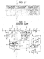
- A related art receiver, such as a television tuner, will be described with reference to FIG. 3. An input tuning circuit 2 is coupled to an input terminal 1 to which a television signal is input. The input tuning circuit 2 includes inductive elements 2a and 2b that are connected in series to each other, a capacitor 2c through which one end of the inductive element 2a is grounded, a varactor diode 2d, an anode of which is connected to the inductive element 2b, and a capacitor 2e through which a cathode of the varactor diode 2d is grounded. A connection point between the inductive element 2a and the capacitor 2c is connected to a ground through a resistor 3. In addition, the cathode of the varactor diode 2d is connected to a tuning voltage terminal 4. The input tuning circuit 2 is coupled to an RF amplifier 7 through a series circuit of a coupling varactor diode 5 and a coupling capacitor 6. An anode of the coupling varactor diode 5 is connected to the anode of the varactor diode 2d, and a cathode thereof is connected to the tuning voltage terminal 4.
- A primary circuit of an interstage tuning circuit 8 coupled to an output of the RF amplifier 7 includes a varactor diode 8a, an
inductive element 8b that is connected to an anode of the varactor diode 8a, and acapacitor 8c through which a cathode of the varactor diode 8a is grounded. A secondary circuit of the interstage tuning circuit 8 also includes a varactor diode 8d, an inductive element 8e that is connected to an anode of the varactor diode 8d, and acapacitor 8f through which a cathode of the varactor diode 8d is grounded. The twoinductive elements 8b and 8e are connected in series to each other, and a connection point between the twoinductive elements 8b and 8e is connected to one end of a coupling inductive element 8g. The other end of the inductive element 8g is grounded through acapacitor 8h. The cathodes of the two varactor diodes 8a and 8d are connected to the tuning voltage terminal 4. In addition, a connection point between the coupling inductive element 8g and thecapacitor 8h is connected to the ground through a resistor 9. - The interstage tuning circuit 8 is coupled to a mixer 12 through a series circuit of a
coupling varactor diode 10 and a capacitor 11. An anode of thecoupling varactor diode 10 is connected to the anode of the varactor diode 8d, and a cathode thereof is connected to the tuning voltage terminal 4. A local oscillating signal is supplied from an oscillator 13 to the mixer 12. And then, a television signal output from the interstage tuning circuit 8 is converted into an intermediate frequency signal by the mixer 12. Aresonating circuit 14 constituting the oscillator 13 includes avaractor diode 14a, acapacitor 14b through which a cathode of thevaractor diode 14a is grounded, an inductive element 14c, one end of which is connected to an anode of thevaractor diode 14a, and acapacitor 14d through which the other end of the inductive element 14c is grounded. The cathode of thevaractor diode 14a is connected to the tuning voltage terminal 4. In addition, a connection point between the inductive element 14c and thecapacitor 14d is connected to the ground through theresistor 15. - The voltage on the anode of the varactor diode 2d in the input tuning circuit 2, the voltage on the anode of each of the two varactor diodes 8a and 8d in the interstage tuning circuit 8, and the voltage on the anode of the
varactor diode 14a in theresonating circuit 14 are switched by atransistor 16. An emitter of thetransistor 16 is grounded, and a predetermined voltage is applied to a collector of thetransistor 16 from a voltage stabilization circuit 17 through aprotection resistor 18. To a base of thetransistor 16, a switching voltage for turning on or off thetransistor 16 is applied. And then, the connection point between the inductive element 2a and the capacitor 2c in the input tuning circuit 2 is connected to the collector of thetransistor 16 through aresistor 19. Further, the connection point between the coupling inductive element 8g and thecapacitor 8h in the interstage tuning circuit 8 is connected to the collector of thetransistor 16 through a resistor 20. In addition, the connection point between the inductive element 14c and thecapacitor 14d in theresonating circuit 14 is connected to the collector of thetransistor 16 through aresistor 21. - Moreover, the oscillation frequency of the oscillator 13 is controlled by a
PLL circuit 25 on the basis of channel selection data D, and, as a result of the control, a tuning voltage Vt is output from thePLL circuit 25 and is supplied to the tuning voltage terminal 4. - Next, according to the configuration described above, when a high-band television signal is received, the
transistor 16 is turned on. If doing so, the anodes of theindividual varactor diodes 2d, 8a, 8d, and 14a have a ground potential. In this state, the tuning voltage Vt is applied to the cathodes of theindividual varactor diodes transistor 16 is turned off. If doing so, a voltage divided by theresistors 19 and 3 is applied to the anode of the varactor diode 2d, a voltage divided by the resistors 20 and 9 is applied to the anodes of the varactor diodes 8a and 8d, and a voltage divided by theresistors varactor diode 14a. Accordingly, the tuning voltage to be applied to the cathodes of the individual varactor diodes is increased, and thus a receiving frequency range can be expanded, without using an unstable low tuning voltage (for example, seeJapanese Utility Model No. 3106132 - In a related art transceiver, the same tuning voltage is applied to the varactor diodes 2d, 8a, and 8d in the tuning circuit and the varactor diode 4a in the oscillator. Accordingly, even when the resistance values of the
resistors resistors 3, 9, and 15 are independently set, in a wide frequency range, a tuning frequency and a local oscillation frequency are rarely changed at the same frequency gap when the tuning voltage is changed. As a result, a so-called tracking error occurs. - It is an object of the invention to provide a receiver which can constantly maintain a predetermined gap between a tuning frequency of a tuning circuit and a local oscillation frequency of an oscillator over a wide receiving frequency range, thereby preventing a tracking error.
- According to an aspect of the invention, a receiver includes a tuning circuit that has a variable capacitive unit and an inductive element, and is capable of being tuned to a frequency of a received signal, the variable capacitive unit having a plurality of capacitive elements and switching units that connect the individual capacitive elements to the inductive element in parallel, a mixer that frequency-converts the received signal, a local oscillator that supplies a local oscillating signal to the mixer, a first PLL circuit that controls the local oscillator to oscillate at a frequency corresponding to the frequency of the received signal, an oscillating active element that constitutes an oscillating circuit together with the tuning circuit, a second PLL circuit that controls the oscillating circuit to output a control voltage for setting a capacitance value of the variable capacitive unit such that an oscillation frequency of the oscillating circuit matches with the frequency of the received signal, an up/down counter that controls turning on/off of the switching units by multiple-bit output data, and a count signal generator that compares the control voltage with a first reference voltage and a second reference voltage lower than the first reference voltage, and outputs an up count signal or a down count signal to the up/down counter. Here, the count signal generator outputs the down count signal when the control voltage is higher than the first reference voltage, outputs the up count signal when the control voltage is lower than the second reference voltage, and stops the output of the up count signal and the down count signal and outputs a lock signal when the control voltage is between the first reference voltage and the second reference voltage. By the lock signal, a flow of a current in the oscillating active element stops.
- The capacitance values of the capacitive elements may be set to be different from one another by setting, with respect to one capacitive element having a minimum capacitance value, the capacitance values of other capacitive elements to be 2N times as much as the minimum capacitance value.
- The count signal generator may have a first comparator that compares the control voltage with the first reference voltage and outputs a high logical level or a low logical level, a second comparator that compares the control voltage with the second reference voltage and outputs a high logical level or a low logical level, and a counter control circuit that outputs one of the up count signal, the down count signal, and the lock signal on the basis of the logical levels output from the first comparator and the second comparator.
- The tuning circuit may be a double-tuning circuit, and each of a primary tuning circuit and a secondary tuning circuit of the double-tuning circuit has the variable capacitive unit and the inductive element. The oscillating active element has two three-terminal amplifying elements, each having an input terminal, an output terminal, and a reference terminal. The primary tuning circuit and the secondary tuning circuit are connected in series to each other and are connected between an output terminal of one of the amplifying elements and an output terminal of the other amplifying element, and a connection point between the primary tuning circuit and the secondary tuning circuit is grounded in a high-frequency manner. An input terminal of one of the amplifying elements is connected to the output terminal of the other amplifying element, and the output terminal of one of the amplifying elements is connected to an input terminal of the other amplifying element. A power supply voltage is applied to the output terminals of the individual amplifying elements through the individual inductive elements, and a constant current source is connected to the reference terminals of the amplifying elements. A flow of a current in the constant current source stops by the lock signal when the control voltage is between the first reference voltage and the second reference voltage.
-
- FIG. 1 is a circuit diagram showing a configuration of a receiver according to the invention;
- FIG. 2 is a truth value table illustrating an operation of a count signal generator in the receiver according to the invention; and
- FIG. 3 is a circuit diagram showing a configuration of a receiver according to the related art.
- Hereinafter, a receiver according to the invention will be described by way of a television tuner. FIG. 1 shows the configuration of the receiver. An input tuning circuit is provided on an upstream side of a high frequency amplifier 31 but is not shown in FIG. 1. A received signal amplified by the high frequency amplifier 31 is input to a frequency-converting
mixer 33 through an interstage tuning circuit 32. A local oscillating signal is supplied from alocal oscillator 34 to themixer 33. Thelocal oscillator 34 is controlled by afirst PLL circuit 35 such that the local oscillating signal has a frequency corresponding to a frequency of the received signal (for example, a frequency higher than a received frequency by an intermediate frequency). The frequency of the local oscillating signal is set by using local oscillation frequency data DLO supplied from a channel-selecting controller 36. Moreover, a reference signal is supplied from a reference oscillator 37 to thefirst PLL circuit 35. - The interstage tuning circuit 32 is a double-tuning circuit. A
primary tuning circuit 32a has an inductive element 41 and a capacitive unit 42. One end of the inductive element 41 is connected to a power supply B, and the capacitive unit 42 is connected between the other end of the inductive element 41 and a ground. The capacitive unit 42 has a plurality of capacitive elements 421 to 424 and switchingunits 425 to 428 that are correspondingly connected to the capacitive elements 421 to 424 in series. Each of the switchingunits 425 to 428 is a three-terminal switching element, such as a FET or a transistor, and a source (or emitter) thereof is grounded. The capacitive element 421 has a minimum capacitance value C, and the capacitance values of thecapacitive elements 422 to 424 are 2C, 4C, and 8C, respectively. That is, the capacitance values of thecapacitive elements 422 to 424 are increased to be 2N times as much as the minimum capacitance value. When the switchingunits 425 to 428 are turned on, the capacitive elements 421 to 424 corresponding to the switchingunits 425 to 428 are connected to the inductive element 41 in parallel in a high-frequency manner. - Similarly, a
secondary tuning circuit 32b has aninductive element 43 and acapacitive unit 44. One end of theinductive element 43 is connected to the power supply B, and thecapacitive unit 44 is connected between the other end of theinductive element 43 and the ground. Thecapacitive unit 44 has a plurality ofcapacitive elements 441 to 444 and switchingunits 445 to 448 that are correspondingly connected to thecapacitive elements 441 to 444 in series. Each of the switchingunits 445 to 448 is a FET, and a source thereof is grounded. Thecapacitive element 441 has a minimum capacitance value C, and the capacitance values of thecapacitive elements 442 to 444 are 2C, 4C, and 8C, respectively. That is, the capacitance values of thecapacitive elements 442 to 444 are increased to be 2N times as much as the minimum capacitance value. When the switchingunits 445 to 448 are turned on, thecapacitive elements 441 to 444 corresponding to the switchingunits 445 to 448 are connected to theinductive element 43 in parallel in a high-frequency manner. In addition, the inductive element 41 of theprimary tuning circuit 32a (hereinafter, referred to as 'primary inductive element') and theinductive element 43 of thesecondary tuning circuit 32b (hereinafter, referred to as 'secondary inductive element') are coupled to each other. - As such, each of the
capacitive units 42 and 43 can have a capacitance value corresponding to an integer multiple of the minimum capacitance value. In addition, by setting the minimum capacitance value as small as possible so as to increase the number of capacitive elements, a tuning frequency can be accurately set and a tuning frequency range can be expanded. - Each of the switching
units 425 to 428 and 445 to 448 is turned on by a voltage applied to its control terminal (gate or base), and the control terminals of the switching units connected to the capacitive elements having the same capacitance value are connected to each other. That is, the control terminals of the switchingunits units units units counter 45. The up/downcounter 45 has the same number of output bits as the number of kinds of capacitive elements. - A first oscillating
active element 46 is provided between the ground and a connection point between the primary inductive element 41 and the capacitive unit 42, and a second oscillating active element 47 is provided between the ground and a connection point between the secondaryinductive element 43 and thecapacitive unit 44. Each of the first oscillatingactive element 46 and the second oscillating active element 47 is a three-terminal amplifying element, such as a FET or a transistor. And then, an output terminal of the first oscillating active element 46 (a drain in case of a FET or a collector in case of a transistor) is connected to the connection point between the primary inductive element 41 and the capacitive unit 42, and an output terminal of the second oscillating active element 47 is connected to the connection point between the secondaryinductive element 43 and thecapacitive unit 44. The output terminal of the first oscillatingactive element 46 is connected to an input terminal of the second oscillating active element 47 (a gate in case of a FET or a base in case of a transistor), and the output terminal of the second oscillating active element 47 is connected to an input terminal of the first oscillatingactive element 46. In addition, a constantcurrent source 48 is provided between a reference terminal of each of the oscillatingactive elements 46 and 47 (a source in case of a FET or a base in case of a transistor) and the ground. A current mirror circuit is used as the constantcurrent source 48. - According to the configuration described above, in a state of being connected in series through the ground, the
primary tuning circuit 32a and thesecondary tuning circuit 32b are connected between the output terminal of the first oscillatingactive element 46 and the output terminal of the second oscillating active element 47. Accordingly, the oscillatingactive elements 46 and 47 and thetuning circuits - The oscillating circuit is controlled by a
second PLL circuit 50 such that an oscillation frequency matches with a frequency of a signal to be received. Thesecond PLL circuit 50 has aprogrammable divider 50a, aphase comparator 50b, acharge pump 50c, and aloop filter 50d. To theprogrammable divider 50a, an oscillating signal is input from the oscillating circuit and received frequency data DRF for setting the frequency of the signal to be received is input from the controller 36. The oscillating signal divided by theprogrammable divider 50a is input to thephase comparator 50b. In thephase comparator 50b, a phase of a reference signal input from the reference oscillator 37 and a phase of the divided oscillating signal are compared with each other, and then an error signal, which is the phase difference, is input to theloop filter 50d through thecharge pump 50c to be then converted into a direct-current (DC) voltage. The DC voltage serves as a control voltage for setting the capacitance values of thecapacitive units 42 and 44. - The control voltage is applied to a count signal generator 51 for supplying an up count signal or a down count signal to the up/down
counter 45. The count signal generator 51 has two comparators 51a and 51b, from which logical levels are output, and a counter control circuit 51c, and the control voltage is input to the first and second comparators 51a and 51b. An output of the first comparator 51a and an output of the second comparator 51b are input to the counter control circuit 51c. A first reference voltage V1 is applied to the first comparator 51a, and a second reference voltage V2 is applied to the second comparator 51b. The second reference voltage V2 is slightly lower than the first reference voltage V1. Accordingly, when the control voltage is higher than the first reference voltage V1, the outputs of the first and second comparators 51a and 51b all become the high levels (H), and when the control voltage is between the first reference voltage V1 and the second reference voltage V2, the output of the first comparator 51a becomes the low level (L) and the output of the second comparator 51b becomes the high level (H). In addition, when the control voltage is lower than the second reference voltage, the outputs of the first and second comparators 51a and 51b all become the low levels (L). - To the counter control circuit 51c, a clock signal (CLCK) is input. In this state, if the logical levels are input from the first and second comparators 51a and 51b, according to a truth value table shown in FIG. 2, the up count signal and the down count signal in synchronization with the clock signal are correspondingly output from the output terminals of the counter control circuit 51c. Further, a high-level lock signal is output from a third output terminal, regardless of the clock signal. That is, when the output of the first comparator 51a and the output of the second comparator 51b all are in the high levels, and, when the output of the first comparator 51a is in the low level and the output of the second comparator 51b is in the high level, only the lock signal is output. In addition, when the output of the first comparator 51a and the output of the second comparator 51b all are in the low levels, only the down count signal is output.
- The up/down
counter 45 performs an up count operation or a down count operation on the basis of the up count signal or the down count signal, and the output terminal of the up/downcounter 45 is changed to a high level or a low level. In addition, a switching unit connected to a high-level output terminal of the up/downcounter 45 is turned on, the capacitive element corresponding to the switching unit is connected to theinductive elements 41 and 43 in parallel, and the oscillating circuit substantially oscillates at a parallel resonance frequency. In this case, the up/down counter 45 continuously performs the up count operation in a range in which the oscillation frequency is higher than the frequency of the signal to be received. Further, the up/down counter 45 continuously performs the down count operation in a range in which the oscillation frequency is lower than the frequency of the signal to be received. In addition, when the oscillation frequency substantially matches with the frequency of the signal to be received, the control voltage becomes a voltage between the first reference voltage V1 and the second reference voltage V2, and thus the counter control circuit 51c outputs the lock signal. By preparing a switching element (not shown) which is turned on by the lock signal and is connected to a collector of a transistor (or a drain in case of a FET) on a constant current input side of a current mirror circuit (not shown) constituting the constantcurrent source 48, it is possible to stop a flow of a constant current. - Accordingly, the operations of the first and second oscillating
active elements 46 and 47 stop, and thus the up count signal and the down count signal are not input to the up/downcounter 45, such that output data (multiple-bit data) of the up/downcounter 45 maintains a value immediately before the operations of the first and second oscillatingactive elements 46 and 47 stop. As a result, thetuning circuits tuning circuits mixer 33. And then, the signal input to themixer 33 is frequency-converted into an intermediate frequency signal. - As described above, the
tuning circuits local oscillator 34. Specifically, thetuning circuits second PLL circuit 50 such that the oscillation frequency matches with the frequency of the signal to be received. Accordingly, a frequency gap between the local oscillation frequency and the tuning frequency can be constantly maintained constant, and thus a so-called tracking error can be prevented. - Moreover, even thought the invention has been described about the control of the tuning frequency in the interstage tuning circuit, the invention can be applied to other tuning circuits, for example, an input tuning circuit.
- According to the first aspect of the invention, the variable capacitive unit has the plurality of capacitive elements and the switching units that connect the individual capacitive elements to the inductive element in parallel. Further, the oscillating active element that constitutes the oscillating circuit together with the tuning circuit, the second PLL circuit that controls the oscillating circuit to output the control voltage for setting the capacitance value of the variable capacitive unit such that the oscillation frequency of the oscillating circuit matches with the frequency of the received signal, the up/down counter that controls turning on/off of the switching units by multiple-bit output data, and the count signal generator that compares the control voltage with the first reference voltage and the second reference voltage lower than the first reference voltage, and outputs the up count signal or the down count signal to the up/down counter are provided. Here, the count signal generator outputs the down count signal when the control voltage is higher than the first reference voltage, outputs the up count signal when the control voltage is lower than the second reference voltage, and stops the output of the up count signal and the down count signal and outputs the lock signal when the control voltage is between the first reference voltage and the second reference voltage. By the lock signal, the flow of the current in the oscillating active element stops. Therefore, the tuning circuit matches with the frequency of the received signal. As a result, a tracking error does not occur between the tuning frequency of the tuning circuit and the oscillation frequency of the local oscillator.
- According to the second aspect of the invention, the capacitance values of the capacitive elements are set to be different from one another by setting, with respect to one capacitive element having a minimum capacitance value, the capacitance values of other capacitive elements to be 2N times as much as the minimum capacitance value. Therefore, the capacitance value of the capacitive unit can be closely set.
- According to the third aspect of the invention, the count signal generator has the first comparator that compares the control voltage with the first reference voltage and outputs the high logical level or the low logical level, the second comparator that compares the control voltage with the second reference voltage and outputs the high logical level or the low logical level, and the counter control circuit that outputs one of the up count signal, the down count signal, and the lock signal on the basis of the logical levels output from the first comparator and the second comparator. Therefore, the capacitance value of the capacitive unit can be maintained when the tuning circuit matches with the frequency of the received signal.
- According to the fourth aspect of the invention, the tuning circuit is the double-tuning circuit, and each of the primary tuning circuit and the secondary tuning circuit of the double-tuning circuit has the variable capacitive unit and the inductive element. The oscillating active element has the two three-terminal amplifying elements, each having the input terminal, the output terminal, and the reference terminal. The primary tuning circuit and the secondary tuning circuit are connected in series to each other and are connected between the output terminal of one of the amplifying elements and the output terminal of the other amplifying element. The connection point between the primary tuning circuit and the secondary tuning circuit is grounded in a high-frequency manner. The input terminal of one of the amplifying elements is connected to the output terminal of the other amplifying element, and the output terminal of one of the amplifying elements is connected to an input terminal of the other amplifying element. The power supply voltage is applied to the output terminals of the individual amplifying elements through the individual inductive elements, and the constant current source is connected to the reference terminals of the amplifying elements. The flow of the current in the constant current source stops by the lock signal when the control voltage is between the first reference voltage and the second reference voltage. Therefore, if the tuning circuit matches with the frequency of the received signal, the oscillating active element does not have influence on the tuning circuit.
Claims (4)
- A receiver comprising:a tuning circuit 32 that has a variable capacitive unit 42 (44) and an inductive element 41 (43), and is capable of being tuned to a frequency of a received signal, the variable capacitive unit 42 (44) having a plurality of capacitive elements 421 to 424 (441 to 444) and switching units 425 to 428 (445 to 448) that connect the individual capacitive elements 421 to 424 (441 to 444) to the inductive element 41 (43) in parallel;a mixer 33 that frequency-converts the received signal;a local oscillator 34 that supplies a local oscillating signal to the mixer 33;a first PLL circuit 35 that controls the local oscillator 34 to oscillate at a frequency corresponding to the frequency of the received signal;an oscillating active element 46 (47) that constitutes an oscillating circuit together with the tuning circuit 32;a second PLL circuit 50 that controls the oscillating circuit to output a control voltage for setting a capacitance value of the variable capacitive unit 42 (44) such that an oscillation frequency of the oscillating circuit matches with the frequency of the received signal;an up/down counter 45 that controls turning on/off of the switching units 425 to 428 (445 to 448) by multiple-bit output data; anda count signal generator 51 that compares the control voltage with a first reference voltage and a second reference voltage lower than the first reference voltage, and outputs an up count signal or a down count signal to the up/down counter 45,characterized in that the count signal generator 51 outputs the down count signal when the control voltage is higher than the first reference voltage, outputs the up count signal when the control voltage is lower than the second reference voltage, and stops the output of the up count signal and the down count signal and outputs a lock signal when the control voltage is between the first reference voltage and the second reference voltage, andby the lock signal, a flow of a current in the oscillating active element 46 (47) stops.
- The receiver according to claim 1,
characterized in that the capacitance values of the capacitive elements 421 to 424 (441 to 444) are set to be different from one another by setting, with respect to one capacitive element 421 (441) having a minimum capacitance value, the capacitance values of other capacitive elements 421 to 424 (442 to 444) to be 2N times as much as the minimum capacitance value. - The receiver according to claim 1 or claim 2,
characterized in that the count signal generator 51 has:a first comparator 51a that compares the control voltage with the first reference voltage and outputs a high logical level or a low logical level;a second comparator 51b that compares the control voltage with the second reference voltage and outputs a high logical level or a low logical level; anda counter control circuit 51c that outputs one of the up count signal, the down count signal, and the lock signal on the basis of the logical levels output from the first comparator 51a and the second comparator 51b. - The receiver according to any preceding claim,
characterized in that the tuning circuit 32 is a double-tuning circuit,
each of a primary tuning circuit 32a and a secondary tuning circuit 32b of the double-tuning circuit has the variable capacitive unit 42 (44) and the inductive element 41 (43),
the oscillating active element 46 (47) has two three-terminal amplifying elements, each having an input terminal, an output terminal, and a reference terminal,
the primary tuning circuit 32a and the secondary tuning circuit 32b are connected in series to each other and are connected between an output terminal of one of the amplifying elements and an output terminal of the other amplifying element,
a connection point between the primary tuning circuit 32a and the secondary tuning circuit 32b is grounded in a high-frequency manner,
an input terminal of one of the amplifying elements is connected to the output terminal of the other amplifying element, and the output terminal of one of the amplifying elements is connected to an input terminal of the other amplifying element,
a power supply voltage is applied to the output terminals of the individual amplifying elements through the individual inductive elements 41 and 43, and a constant current source 48 is connected to the reference terminals of the amplifying elements, and
a flow of a current in the constant current source 48 stops by the lock signal when the control voltage is between the first reference voltage and the second reference voltage.
Applications Claiming Priority (1)
| Application Number | Priority Date | Filing Date | Title |
|---|---|---|---|
| JP2005102819A JP4699791B2 (en) | 2005-03-31 | 2005-03-31 | Receiver |
Publications (2)
| Publication Number | Publication Date |
|---|---|
| EP1708500A2 true EP1708500A2 (en) | 2006-10-04 |
| EP1708500A3 EP1708500A3 (en) | 2008-07-30 |
Family
ID=36677186
Family Applications (1)
| Application Number | Title | Priority Date | Filing Date |
|---|---|---|---|
| EP06110324A Withdrawn EP1708500A3 (en) | 2005-03-31 | 2006-02-23 | Receiver having no tracking error |
Country Status (3)
| Country | Link |
|---|---|
| US (1) | US7355490B2 (en) |
| EP (1) | EP1708500A3 (en) |
| JP (1) | JP4699791B2 (en) |
Families Citing this family (1)
| Publication number | Priority date | Publication date | Assignee | Title |
|---|---|---|---|---|
| JP4310661B2 (en) | 2007-02-05 | 2009-08-12 | ソニー株式会社 | IC for tuning circuit and receiving circuit using the same |
Citations (3)
| Publication number | Priority date | Publication date | Assignee | Title |
|---|---|---|---|---|
| JPH03106132A (en) | 1989-09-20 | 1991-05-02 | Hitachi Ltd | Level diamond control method |
| WO2000067325A1 (en) | 1999-05-03 | 2000-11-09 | Silicon Wave, Inc. | Method and apparatus for digitally controlling the capacitance of an integrated circuit device using mos field-effect transistors |
| WO2003103143A1 (en) | 2002-05-29 | 2003-12-11 | Ukom, Inc. | Methods and apparatus for tuning using successive aproximation |
Family Cites Families (10)
| Publication number | Priority date | Publication date | Assignee | Title |
|---|---|---|---|---|
| JPH0621767A (en) | 1992-06-30 | 1994-01-28 | Victor Co Of Japan Ltd | Tuner tracking device |
| JP3055399B2 (en) * | 1994-07-27 | 2000-06-26 | 松下電器産業株式会社 | High frequency signal processing unit |
| US5648744A (en) * | 1995-12-22 | 1997-07-15 | Microtune, Inc. | System and method for voltage controlled oscillator automatic band selection |
| US6522868B1 (en) * | 1998-11-04 | 2003-02-18 | Lockheed Martin Corporation | Method and apparatus for generating a communication band signal with reduced phase noise |
| AU2147900A (en) * | 1998-11-12 | 2000-05-29 | Broadcom Corporation | Fully integrated tuner architecture |
| JP2001274711A (en) * | 2000-03-27 | 2001-10-05 | Clarion Co Ltd | Broadcast receiver |
| JP2002271193A (en) * | 2001-03-06 | 2002-09-20 | Fujitsu Ltd | Phase locked oscillator and communication device |
| DE10156027B4 (en) * | 2001-11-15 | 2012-02-09 | Globalfoundries Inc. | Adjustable filter circuit |
| US6856205B1 (en) * | 2002-04-17 | 2005-02-15 | Sequoia Communications | VCO with automatic calibration |
| JP3893338B2 (en) * | 2002-09-09 | 2007-03-14 | 株式会社ケンウッド | Radio receiver |
-
2005
- 2005-03-31 JP JP2005102819A patent/JP4699791B2/en not_active Expired - Fee Related
-
2006
- 2006-02-23 EP EP06110324A patent/EP1708500A3/en not_active Withdrawn
- 2006-03-23 US US11/389,427 patent/US7355490B2/en not_active Expired - Fee Related
Patent Citations (3)
| Publication number | Priority date | Publication date | Assignee | Title |
|---|---|---|---|---|
| JPH03106132A (en) | 1989-09-20 | 1991-05-02 | Hitachi Ltd | Level diamond control method |
| WO2000067325A1 (en) | 1999-05-03 | 2000-11-09 | Silicon Wave, Inc. | Method and apparatus for digitally controlling the capacitance of an integrated circuit device using mos field-effect transistors |
| WO2003103143A1 (en) | 2002-05-29 | 2003-12-11 | Ukom, Inc. | Methods and apparatus for tuning using successive aproximation |
Also Published As
| Publication number | Publication date |
|---|---|
| JP2006287459A (en) | 2006-10-19 |
| EP1708500A3 (en) | 2008-07-30 |
| US7355490B2 (en) | 2008-04-08 |
| JP4699791B2 (en) | 2011-06-15 |
| US20060223475A1 (en) | 2006-10-05 |
Similar Documents
| Publication | Publication Date | Title |
|---|---|---|
| US6496075B2 (en) | Automatic tuning of VCO | |
| US7902929B2 (en) | Analogue self-calibration method and apparatus for low noise, fast and wide-locking range phase locked loop | |
| US4598423A (en) | Tuning circuit for a multiband tuner | |
| US6853257B2 (en) | PLL circuit including a voltage controlled oscillator and a method for controlling a voltage controlled oscillator | |
| US20080238495A1 (en) | Frequency synthesizer and wireless communication device utilizing the same | |
| US7259638B2 (en) | Voltage controlled oscillator and semiconductor integrated circuit for communication | |
| US7170358B2 (en) | Voltage controlled oscillator, and PLL circuit and wireless communication apparatus using the same | |
| US20120142283A1 (en) | Wireless communication apparatus | |
| US20060152290A1 (en) | Apparatus and method of oscillating wideband frequency | |
| US6853262B2 (en) | Voltage-controlled oscillator circuit which compensates for supply voltage fluctuations | |
| US6927637B1 (en) | Efficient tuning circuit for on-chip voltage controlled oscillator and method | |
| US6157821A (en) | Voltage step up for a low voltage frequency synthesizer architecture | |
| US5905414A (en) | VCO having control voltage and modulation signal applied to varactor | |
| JP2842847B2 (en) | PLL synthesizer circuit | |
| US6724273B1 (en) | Filter circuitry for voltage controlled oscillator | |
| US7501907B1 (en) | Self-biased active VCO level shifter | |
| US7355490B2 (en) | Receiver having no tracking error | |
| JP2007013898A (en) | PLL frequency synthesizer, integrated circuit and communication device using the same | |
| JPH0241934B2 (en) | ||
| US20020109555A1 (en) | Voltage-controlled variable tuning circuit for switching an oscillation frequency band of a voltage controlled oscillator | |
| US6624709B2 (en) | Voltage-controlled oscillator and electronic device using the same | |
| US20130063661A1 (en) | Phase synchronication circuit and television signal reception circuit | |
| US7573970B2 (en) | Prescaler and buffer | |
| US20090079880A1 (en) | Television Tuner | |
| US7363015B2 (en) | Wide-frequency-range television tuner |
Legal Events
| Date | Code | Title | Description |
|---|---|---|---|
| PUAI | Public reference made under article 153(3) epc to a published international application that has entered the european phase |
Free format text: ORIGINAL CODE: 0009012 |
|
| AK | Designated contracting states |
Kind code of ref document: A2 Designated state(s): AT BE BG CH CY CZ DE DK EE ES FI FR GB GR HU IE IS IT LI LT LU LV MC NL PL PT RO SE SI SK TR |
|
| AX | Request for extension of the european patent |
Extension state: AL BA HR MK YU |
|
| PUAL | Search report despatched |
Free format text: ORIGINAL CODE: 0009013 |
|
| AK | Designated contracting states |
Kind code of ref document: A3 Designated state(s): AT BE BG CH CY CZ DE DK EE ES FI FR GB GR HU IE IS IT LI LT LU LV MC NL PL PT RO SE SI SK TR |
|
| AX | Request for extension of the european patent |
Extension state: AL BA HR MK YU |
|
| 17P | Request for examination filed |
Effective date: 20080909 |
|
| 17Q | First examination report despatched |
Effective date: 20081117 |
|
| AKX | Designation fees paid |
Designated state(s): DE FR GB |
|
| STAA | Information on the status of an ep patent application or granted ep patent |
Free format text: STATUS: THE APPLICATION HAS BEEN WITHDRAWN |
|
| 18W | Application withdrawn |
Effective date: 20140328 |