EP1705922A2 - Quantization circuit - Google Patents
Quantization circuit Download PDFInfo
- Publication number
- EP1705922A2 EP1705922A2 EP20060013939 EP06013939A EP1705922A2 EP 1705922 A2 EP1705922 A2 EP 1705922A2 EP 20060013939 EP20060013939 EP 20060013939 EP 06013939 A EP06013939 A EP 06013939A EP 1705922 A2 EP1705922 A2 EP 1705922A2
- Authority
- EP
- European Patent Office
- Prior art keywords
- analog
- circuit
- voltage
- dct
- dimensional
- Prior art date
- Legal status (The legal status is an assumption and is not a legal conclusion. Google has not performed a legal analysis and makes no representation as to the accuracy of the status listed.)
- Withdrawn
Links
Images


Classifications
-
- H—ELECTRICITY
- H03—ELECTRONIC CIRCUITRY
- H03M—CODING; DECODING; CODE CONVERSION IN GENERAL
- H03M7/00—Conversion of a code where information is represented by a given sequence or number of digits to a code where the same, similar or subset of information is represented by a different sequence or number of digits
- H03M7/30—Compression; Expansion; Suppression of unnecessary data, e.g. redundancy reduction
- H03M7/40—Conversion to or from variable length codes, e.g. Shannon-Fano code, Huffman code, Morse code
- H03M7/42—Conversion to or from variable length codes, e.g. Shannon-Fano code, Huffman code, Morse code using table look-up for the coding or decoding process, e.g. using read-only memory
-
- H—ELECTRICITY
- H04—ELECTRIC COMMUNICATION TECHNIQUE
- H04N—PICTORIAL COMMUNICATION, e.g. TELEVISION
- H04N7/00—Television systems
- H04N7/12—Systems in which the television signal is transmitted via one channel or a plurality of parallel channels, the bandwidth of each channel being less than the bandwidth of the television signal
-
- H—ELECTRICITY
- H04—ELECTRIC COMMUNICATION TECHNIQUE
- H04N—PICTORIAL COMMUNICATION, e.g. TELEVISION
- H04N19/00—Methods or arrangements for coding, decoding, compressing or decompressing digital video signals
- H04N19/10—Methods or arrangements for coding, decoding, compressing or decompressing digital video signals using adaptive coding
- H04N19/102—Methods or arrangements for coding, decoding, compressing or decompressing digital video signals using adaptive coding characterised by the element, parameter or selection affected or controlled by the adaptive coding
- H04N19/124—Quantisation
- H04N19/126—Details of normalisation or weighting functions, e.g. normalisation matrices or variable uniform quantisers
-
- H—ELECTRICITY
- H04—ELECTRIC COMMUNICATION TECHNIQUE
- H04N—PICTORIAL COMMUNICATION, e.g. TELEVISION
- H04N19/00—Methods or arrangements for coding, decoding, compressing or decompressing digital video signals
- H04N19/60—Methods or arrangements for coding, decoding, compressing or decompressing digital video signals using transform coding
-
- H—ELECTRICITY
- H04—ELECTRIC COMMUNICATION TECHNIQUE
- H04N—PICTORIAL COMMUNICATION, e.g. TELEVISION
- H04N19/00—Methods or arrangements for coding, decoding, compressing or decompressing digital video signals
- H04N19/10—Methods or arrangements for coding, decoding, compressing or decompressing digital video signals using adaptive coding
- H04N19/102—Methods or arrangements for coding, decoding, compressing or decompressing digital video signals using adaptive coding characterised by the element, parameter or selection affected or controlled by the adaptive coding
- H04N19/124—Quantisation
Definitions
- FIGURE 5 shows the internal organization of the analog sum-of-products arithmetic unit 21.6 of FIGURE 4.
- the arithmetic unit 21.6 of FIGURE 5 has a row of polarity change switches 101, a row of input switches 102, a row of capacitors 103, an operational amplifier 104, a feedback capacitor 105, and an equalizing switch 106.
- the switch 23 of FIGURE 4 now establishes connection to the image sensing element 10.
- the capacitor row 103 is formed of eight capacitors having respective values C0, C1, C2, C3, C4, C5, C6, and C7 which are weighted respectively f, b, b, f, f, b, b, and f, and the value of the feedback capacitor 105, Cf, is weighed 4.
- FIGURE 7 shows a part of the internal organization of the ADC circuit 31 of FIGURE 2.
- An ADC 41 which is a major unit of the ADC circuit 31, has a row of resistors 42 disposed to divide the reference voltage S ⁇ Vref to generate a plurality of internal reference voltages, and an ADC core 43.
- the circuit of FIGURE 7 further includes a comparator 44 disposed to make a comparison between Z (the input voltage) and Vmin (the minimum reference voltage of the internal reference voltages corresponding to a 1LSB) and a switch 45 coupled to an output of the comparator 44 and connected between the ADC core 43 and a power supply 46 so as to control the supply of power to the ADC core 43.
- Z the input voltage
- Vmin the minimum reference voltage of the internal reference voltages corresponding to a 1LSB
- FIGURE 10 shows a modification example in differential input/output form of the analog sum-of-products arithmetic unit 21.6 in single signal form shown in FIGURE 5. Shown in FIGURE 10 are a row of polarity change switches 201, a row of input equalizing switches 202, a row of capacitors 203, an operational amplifier 204, feedback capacitors 205a and 205b, and output equalizing switches 206a and 206b. In accordance with the analog sum-of-products arithmetic unit of FIGURE 10, it is unnecessary for the polarity change switch row 201 to have inverting amplifiers.
Landscapes
- Engineering & Computer Science (AREA)
- Multimedia (AREA)
- Signal Processing (AREA)
- Theoretical Computer Science (AREA)
- Analogue/Digital Conversion (AREA)
- Compression Or Coding Systems Of Tv Signals (AREA)
- Compression, Expansion, Code Conversion, And Decoders (AREA)
- Compression Of Band Width Or Redundancy In Fax (AREA)
- Complex Calculations (AREA)
Abstract
Description
- This invention relates to an image encoding apparatus for compression of information of images.
- Various image encoding apparatus by means of discrete cosine transform (DCT) have been known in the art. Conventionally, an image encoding apparatus includes a two-dimensional digital DCT circuit and a quantization circuit formed by a digital division operation unit and employs digital processing technology. A series of analog signals from an image sensing element such as a CCD (charged-coupled device) is converted by an ADC (analog-to-digital converter) into a series of digital signals. The digital signal series is temporarily held in an image memory. In the two-dimensional digital DCT circuit a two-dimensional DCT is performed on the digital signal series applied from the image memory in pixel blocks. In order to quantize a result of the two-dimensional DCT performed by the two-dimensional digital DCT circuit, the quantization circuit carries out a division operation of dividing a digital value representing the transform result by a quantization coefficient Q.
- However, a disadvantage of the above-described image encoding apparatus is that both the two-dimensional digital DCT circuit and the quantization circuit, formed of a digital division operation unit, are large in circuit scale. This means that there is still room for improvement of the conventional image encoding apparatus, to provide, a compact, low-power, and low-cost image encoding apparatus.
- Accordingly, it is an object of the present invention to provide an improved image encoding apparatus employing an analog processing technique which is attractive for the realization of a reduction in circuit size, a reduction in power consumption, and a reduction in product cost.
- In order to achieve the object, the present invention employs an organization that is formed of an image sensing element for providing a series of voltage signals corresponding to a two-dimensional image, a two-dimensional analog DCT circuit for performing, in pixel blocks, a two-dimensional DCT on a series of voltage signals applied from the image sensing element, and a quantization circuit for quantizing a result of the two-dimensional DCT performed by the two-dimensional analog DCT circuit. The two-dimensional analog DCT circuit has a row of analog sum-of-products arithmetic units for performing a one-dimensional DCT, and an analog memory array for holding a series of output voltage signals of the analog sum-of-products arithmetic unit row corresponding to a series of voltage signals from the image sensing element and for applying a series of voltage signals obtained by transposing a matrix formed of the output voltage signal series to the analog sum-of-products arithmetic unit row. According to Equation (1), shown below, and using a voltage S·Vref as a reference voltage which is S times greater than a fixed voltage Vref, the quantization circuit converts a voltage which is a representation of a transform result of the two-dimensional analog DCT circuit, into a digital value.

In the quantization circuit the digital value is shifted N bits to the right. The quantization circuit is formed of an ADC circuit for converting a voltage representing a transform result of the two-dimensional analog DCT circuit into to a digital value, a decoder for generating signals N and S which satisfy Equation (1) from the quantization coefficient Q, a DAC (digital-to-analog converter) for applying the reference voltage S·Vref (Vref = fixed voltage) corresponding to the signal S to the ADC circuit, and a shifter for performing a process of right-shifting the digital value, obtained in the ADC circuit, N bits corresponding to the signal N. - Generally, signals, converted from spatial components to frequency components by two-dimensional DCT, are ones in which electric power is concentrated in low frequency ranges. Further, the human vision system is less sensitive to the higher frequency components of an image than to the lower frequency components. This characteristic of the human vision system is utilized. That is, lower frequency components are quantized with a higher precision while on the other hand higher frequency components are quantized with a lower precision, to perform compression of image information. Additionally, it is required that the quantization coefficient Q is made variable according to the degree of DCT and the rate of data required in order that adaptive quantization may be carried out.
- Here, the voltage that represents a transform result of the two-dimensional analog DCT circuit is Z. If division by the quantization coefficient Q is performed at the same time that the voltage Z is converted into a digital value R of n bits using the reference voltage Vref, then Equation (2) is obtained.

where [x] is the largest integer that does not exceed a real number x. From Equation (1), Equation (3) is obtained as follows.
That is to say, the following equations (4) and (5) hold.

The voltage Z is converted into a digital value P of n bits using the reference voltage S·Vref and the digital value P is right-shifted N bits, whereby the digital value R representing a result of the quantization can be obtained. - As described above, in accordance with the present invention, analog processing technology is employed in the two-dimensional DCT processing and part of the quantization processing for the realization of compact, low-power, and low-cost image encoding apparatus. Additionally, it is arranged such that series of voltage signals applied from the image sensing element are passed to none of the ADC and the image memory but are directly processed in the two-dimensional analog DCT circuit, and the result of the two-dimensional DCT is further processed in the quantization circuit. Such arrangement makes it easy to integrate the image sensing element, the two-dimensional analog DCT and the quantization circuit on a single chip.
-
- FIGURE 1 is a perspective view showing an appearance of a mobile multimedia computer with a camera head containing therein a one-chip image encoding apparatus according to the present invention.
- FIGURE 2 outlines in block form a one-chip image encoding apparatus in accordance with one embodiment of the present invention.
- FIGURE 3 details a sum-of-products arithmetic operation that is performed in a two-dimensional analog DCT circuit of FIGURE 2.
- FIGURE 4 shows in block form the internal organization of the two-dimensional analog DCT circuit of FIGURE 2.
- FIGURE 5 is a circuit diagram showing the internal organization of one analog sum-of-products arithmetic unit of FIGURE 4.
- FIGURE 6 is a circuit diagram showing the internal organization of an analog memory array of FIGURE 4.
- FIGURE 7 is a circuit diagram showing a part of the internal organization of an ADC circuit of FIGURE 2.
- FIGURE 8 is a circuit diagram showing the internal organization of a decoder of FIGURE 2.
- FIGURE 9 is a circuit diagram showing the internal organization of a shifter of FIGURE 2.
- FIGURE 10 is a circuit diagram showing a modification of the analog sum-of-products arithmetic unit.
- FIGURE 1 shows a mobile multimedia computer. This computer has a
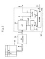
computer section 1, acamera head 2 containing therein a one-chip image encoding apparatus in accordance with the present invention, acable 3 for establishing connection between thecomputer section 1 and thecamera head 2. - FIGURE 2 outlines the one-chip image encoding apparatus which is contained in the
camera head 2. This apparatus is formed by integration of animage sensing element 10, a two-dimensionalanalog DCT circuit 20, and aquantization circuit 30 on a single semiconductor chip. - The
image sensing element 10 is formed by, for example, a CMOS image sensor and provides a series of voltage signals W to the two-dimensionalanalog DCT circuit 20 in which one block of 8 × 8 pixels of an entire two-dimensional image forms a unit. If i and j take a value ranging from 0 to 7, then 8 × 8 voltage signals h(i,j) are applied as the voltage signal series W to the two-dimensionalanalog DCT circuit 20. At this time, eight voltage signals h(0, j) to h(7, j) are supplied as voltage signals W0 to W7 of Group j in parallel with one another. The two-dimensionalanalog DCT circuit 20 performs a two-dimensional DCT on the voltage signal series W. - Here, the two-dimensional DCT is described. The two-dimensional DCT of the 8 × 8 voltage signals h(i,j) can be given by:

where u and v take a value ranging from 0 to 7. C(0) is equal to 2-1/2. If u ≠ 0, then C(u) = 1. If v ≠ 0, then C(v) = 1. Here, Hj(u) is given by:
where j and u take a value ranging from 0 to 7. Equation (6) is changed to:
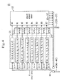
A two-dimensional DCT can be implemented by finding Hj(u) by multiplications of h(0,j) to h(7,j) by respective coefficients and by summing the products according to Equation (7), and by performing the same arithmetic operations on H0(u) to H7(u). If a = cos(π/16) = 0. 9808, b =cos(π/8) = 0. 9239, c = cos(3 π/16) = 0. 8315, d = cos(π/4) = 0. 7071, e = cos(5π/16) = 0. 5556, f = cos(3π/8) = 0. 3827, and g = cos(7π/16) = 0. 1951, this makes it possible to express Equation (7) as shown in FIGURE 3. - Referring to FIGURE 2, when u and v each take a value ranging from 0 to 7, 8
X 8 voltage signals H(u,v) are applied as a series of voltage signals Z to thequantization circuit 30. At this time, eight voltage signals H(0,v) to H(7,v) are supplied in parallel with one another as voltage signals Z0 to Z7 of Group v. Thequantization circuit 30 provides the digital values R representing quantization results of voltages of the voltage signal series Z. - The
quantization circuit 30 has anADC circuit 31, adecoder 32, aDAC 33, and ashifter 34. TheADC circuit 31 is disposed to convert the voltage signal series Z representing a transform result of the two-dimensionalanalog DCT circuit 20 into digital values P each of which consists of four bits. Thedecoder 32 is disposed to generate from the quantization coefficient Q of four bits a shift amount control signal N of four bits and a reference voltage control signal S of four bits, the signals N and S satisfying Q = 2N·S (1 ≦ S < 2). TheDAC 33 is disposed to provide the reference voltage S·Vref (Vref = fixed voltage) corresponding to the reference voltage control signal S to theADC circuit 31. Theshifter 34 is disposed to perform a process of right-shifting a digital value P from the ADC circuit 31 N bits corresponding to the shift amount control signal N, to obtain an output digital value R of four bits. In thequantization circuit 30 the signals N and S which satisfy Equation (1) are generated from the quantization coefficient Q, the voltage signal series Z is converted into the digital values P using the reference voltage S·Vref according to Equation (4), and a process of right-shifting the digital values P N bits is carried out according to Equation (5), for obtaining the output digital values R representing quantization results. - The one-chip image encoding apparatus, shown in FIGURE 2, is provided with external devices, namely a variable length encoder and a data buffer for use in rate control. The variable length encoder receives the digital value R from the
shifter 34. The data buffer outputs encoded data received from the variable length encoder and provides the quantization coefficient Q to thedecoder 32. At this time, the rate control of encoding is achieved by a change in the quantization coefficient Q. - The two-dimensional
analog DCT circuit 20, theADC circuit 31, thedecoder 32, and theshifter 34 are described. - Referring now to FIGURE 4, the internal organization of the two-dimensional
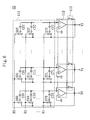
analog DCT circuit 20 of FIGURE 2 is illustrated. Thecircuit 20 of FIGURE 4 has a row of analog sum-of-productsarithmetic units 21 for performing one-dimensional DCT and ananalog memory array 22 for performing matrix transposition. Theanalog memory array 22 holds a series of output voltage signals X of the analog sum-of-productsarithmetic unit row 21 corresponding to a series of voltage signals W from theimage sensing element 10 and provides a series of voltage signals Y, obtained by transposing a matrix formed of the output voltage signal series X, to the analog sum-of-productsarithmetic unit row 21. Aswitch 23, shown in FIGURE 4, is disposed to select between the voltage signal series W from theimage sensing element 10 and the voltage signal series Y from theanalog memory array 22 and to provide W or Y, whichever is selected, as a series of input signals V to the analog sum-of-productsarithmetic unit row 21. The analog sum-of-productsarithmetic unit row 21 is formed of eight analog sum-of-products arithmetic units 21.0 to 21.7 so as to calculate Equation (7), that is, the matrix arithmetic operations of FIGURE 3. The output voltage signal series Z of the analog sum-of-productsarithmetic unit row 21 corresponding to the voltage signal series Y from theanalog memory array 22 is passed via a row ofswitches 24 to thequantization circuit 30. - FIGURE 5 shows the internal organization of the analog sum-of-products arithmetic unit 21.6 of FIGURE 4. The arithmetic unit 21.6 of FIGURE 5 has a row of polarity change switches 101, a row of input switches 102, a row of
capacitors 103, anoperational amplifier 104, afeedback capacitor 105, and an equalizingswitch 106. Suppose here that theswitch 23 of FIGURE 4 now establishes connection to theimage sensing element 10. In other words, V0=h(0.j), V1 = h(1,j), V2 = h(2,j), V3 = h(3,j), V4 = h(4,j), V5 = h(5,j), V6 = h(6,j), and V7 = h(7,j). The polaritychange switch row 101 is provided with inverting amplifiers for inverting V0, V2, V5, and V7 of the eight voltage signals (VO to V7). Thecapacitor row 103 is formed of eight capacitors having respective values C0, C1, C2, C3, C4, C5, C6, and C7 which are weighted respectively f, b, b, f, f, b, b, and f, and the value of thefeedback capacitor 105, Cf, is weighed 4. In the analog sum-of-products arithmetic unit 21.6, the equalizingswitch 106 is closed, theinput switch row 102 forms connection to the signals, and the voltage signals V0 to V7 are applied to thecapacitor row 103. Thereafter, the equalizingswitch 106 is released, and when theinput switch row 102 forms connection to the ground a desired voltage signal X6 (= Hj(6)) is obtained from theoperational amplifier 104 constructing an addition operation circuit. - Referring now to FIGURE 6, the internal organization of the
analog memory array 22 of FIGURE 4 is illustrated. Shown in FIGURE 6 are a row of switches/capacitors 111, a row ofoperational amplifiers 112, and a row of feedback switches 113. The switch/capacitor row 111 is formed of 8 × 8 (=64) switches S00 to S77 and 8 × 8 (=64) capacitors C00 to C77. In theanalog memory array 22 thefeedback switch row 113 is closed during the write operation. By switching of the switch/capacitor row 111, voltage signals X0, X1,..., and X7 ofGroup 1 are stored in the eight capacitors C00, C10,..., and C70, respectively, voltage signals X0, X1,..., and X7 ofGroup 2 are stored in the eight capacitors C01, C11,..., and C71, respectively and so on. Finally, voltage signals X0, X1,..., and X7 ofGroup 8 are stored in the eight capacitors C07, C17,..., and C77, respectively. During the read operation, thefeedback switch row 113 is released. Voltages, held in the eight capacitors C00, C01, ..., and C07, are read out as voltage signals Y0, Y1,..., and Y7 ofGroup 1 by theoperational amplifier row 112, voltages, held in the eight capacitors C10, C11, ..., and C17, are read out as voltage signals Y0, Y1,..., and Y7 ofGroup 2 and so on. Finally, voltages, held in the eight capacitors C70, C71, ..., and C77 are read out as voltage signals Y0, Y1,..., and Y7 ofGroup 8. In this way, a matrix transposition relating to the voltage signal series is implemented. - FIGURE 7 shows a part of the internal organization of the
ADC circuit 31 of FIGURE 2. AnADC 41, which is a major unit of theADC circuit 31, has a row ofresistors 42 disposed to divide the reference voltage S·Vref to generate a plurality of internal reference voltages, and anADC core 43. The circuit of FIGURE 7 further includes acomparator 44 disposed to make a comparison between Z (the input voltage) and Vmin (the minimum reference voltage of the internal reference voltages corresponding to a 1LSB) and aswitch 45 coupled to an output of thecomparator 44 and connected between theADC core 43 and apower supply 46 so as to control the supply of power to theADC core 43. In order to hold the power consumption low, it is arranged such that theADC core 43 stops operating when Z ≦ Vmin. - Concrete examples of the quantization coefficient Q (Q = 2N. S (1 ≦ S < 2)), the shift amount control signal N, and the reference voltage control signal S are described. Q and S are expressed in binary notation. N is expressed in decimal notation.
- (1) If Q = 0001, then N = 0 and S = 1. 000
- (2) If Q = 0010, then N = 1 and S = 1. 000
If Q = 0011, then N = 1 and S = 1. 100 - (3) If Q = 0100, then N = 2 and S = 1. 000
If Q = 0101, then N = 2 and S = 1. 010
If Q = 0110, then N = 2 and S = 1. 100
If Q = 0111, then N = 2 and S = 1. 110 - (4) If Q = 1000, then N = 3 and S = 1. 000
If Q = 1001, then N = 3 and S = 1. 001
If Q = 1010, then N = 3 and S = 1. 010
If Q = 1011, then N = 3 and S = 1. 011
If Q = 1100, then N = 3 and S = 1. 100
If Q = 1101, then N = 3 and S = 1. 101
If Q = 1110, then N = 3 and S = 1. 110
If Q = 1111, then N = 3 and S = 1. 111 - FIGURE 8 shows the internal organization of the
decoder 32 of FIGURE 2. Thedecoder 32 of FIGURE 8 has a group ofswitches 51 and a row oflogical circuits 52. Thelogical circuit row 52 generates four bits N3, N2, N1, and N0 together forming the shift amount control signal N from four bits Q3, Q2, Q1, and Q0 together forming the quantization coefficient Q. N0 = 1, N1 = 1, N2 = 1, and N3 = 1 mean N = 0, N = 1, N = 2, and N = 3, respectively. According to the shift amount control signal N, theswitch group 51 generates four bits S3, S2, S1, and S0 together forming the reference voltage control signal S from Q3, Q2, Q1, and Q0. For instance, if Q = 0101, N2 = 1 is obtained in thelogical circuit row 52 and S = 1. 010 is obtained by a process of left-shifting Q one bit in theswitch group 51. Referring to the fixed voltage Vref, theDAC 33 of FIGURE 2 converts the reference voltage control signal S into an analog signal, to provide the variable reference voltage S·Vref to theADC circuit 31. - FIGURE 9 shows the internal organization of the
shifter 34 of FIGURE 2. Thesifter 34 of FIGURE 9 is formed of a group of switches 53. According to the shift amount control signal N, theswitch group 53 generates four bits R3, R2, R1, and R0 together forming the output digital value R of thequantization circuit 30 from four bits P3, P2, P1, and P0 together forming the output digital value P of theADC circuit 31. For example, if P = 0100 and N2 = 1, R = 0001 is obtained by a process of right-shifting P two bits in theswitch group 53. - As described above, in accordance with the embodiment of FIGURE 2, analog processing is employed in the two-dimensional DCT and part of the quantization for the realization of compact, low-power, and low-cost image encoding apparatus. Series of voltage signals applied from the
image sensing element 10 are passed to none of the ADC and the image memory but are directly processed in the two-dimensionalanalog DCT circuit 20, which makes it easy to integrate theimage sensing element 10, the two-dimensionalanalog DCT circuit 20, and thequantization circuit 30 on a single chip. In order to stop theADC 41 when in thequantization circuit 30 the input voltage Z of theADC 41 is detected to fall below the predetermined voltage Vmin, power control means 44 and 45 are provided. This achieves a considerable reduction of the power consumption thereby providing an image encoding apparatus suitable for, for example, mobile videotelephones and mobile computers. - In the foregoing description, the circuit organization is a single signal form; however, it may be a differential circuit form. FIGURE 10 shows a modification example in differential input/output form of the analog sum-of-products arithmetic unit 21.6 in single signal form shown in FIGURE 5. Shown in FIGURE 10 are a row of polarity change switches 201, a row of
input equalizing switches 202, a row ofcapacitors 203, anoperational amplifier 204,feedback capacitors output equalizing switches change switch row 201 to have inverting amplifiers. - It may be arranged such that two two-dimensional analog DCT circuits are disposed between the
image sensing element 10 and thequantization circuit 30, and while one of the two two-dimensional analog DCT circuits supplies the voltage signal series Z to thequantization circuit 30 the other two-dimensional analog DCT circuit receives the voltage signal series W from theimage sensing element 10. These two two-dimensional analog DCT circuits provide in alternating manner the voltage signal series Z to thequantization circuit 30. This accordingly allows thequantization circuit 30 to continuously operate. - The number of bits forming the digital value P or the digital value R may be an arbitrary number. Likewise, the number of bits forming the quantization coefficient Q, the shift amount control signal N, or the reference voltage control signal S may be an arbitrary number.
Claims (3)
- A quantization circuit comprising:an analog-to-digital conversion circuit for converting an input voltage into a digital value;a decoder for generating signals N and S which satisfy Q = 2 N.S (1 < = S < 2) from a given quantization coefficient Q;a digital-to-analog converter for providing, by making reference to a fixed voltage Vref, a reference voltage S.Vref corresponding to said signal S generated by said decoder, to said analog-to-digital conversion circuit; anda shifter for right-shifting said digital value produced by said analog-to-digital conversion circuit N bits according to said signal N generated by said decoder.
- The quantization circuit of claim 1,
said analog-to-digital conversion circuit including:an analog-to-digital converter for converting a voltage representing a transform result of said two-dimensional analog discrete cosine transform circuit into a digital value; andpower control means for controlling said analog-to-digital converter to stop operating when an input voltage to said analog-to-digital converter is detected to fall below a predetermined voltage. - The quantization circuit of claim 1 or 2,
said power control means including:a comparator for making a comparison between an input voltage to said analog-to-digital converter and the minimum reference voltage of a plurality of internal reference voltages obtained by division of said reference voltage S.Vref supplied from said digital-to-analog converter; anda switch which is coupled to an output of said comparator in order to control the supply of power to said analog-to-digital converter.
Applications Claiming Priority (2)
| Application Number | Priority Date | Filing Date | Title |
|---|---|---|---|
| JP26856196A JPH10117350A (en) | 1996-10-09 | 1996-10-09 | Image coder adopting analog processing system |
| EP19970117052 EP0836322B1 (en) | 1996-10-09 | 1997-10-01 | Image encoding apparatus employing analog processing system |
Related Parent Applications (1)
| Application Number | Title | Priority Date | Filing Date |
|---|---|---|---|
| EP19970117052 Division EP0836322B1 (en) | 1996-10-09 | 1997-10-01 | Image encoding apparatus employing analog processing system |
Publications (2)
| Publication Number | Publication Date |
|---|---|
| EP1705922A2 true EP1705922A2 (en) | 2006-09-27 |
| EP1705922A3 EP1705922A3 (en) | 2008-03-19 |
Family
ID=17460243
Family Applications (3)
| Application Number | Title | Priority Date | Filing Date |
|---|---|---|---|
| EP20060013939 Withdrawn EP1705922A3 (en) | 1996-10-09 | 1997-10-01 | Quantization circuit |
| EP19970117052 Expired - Lifetime EP0836322B1 (en) | 1996-10-09 | 1997-10-01 | Image encoding apparatus employing analog processing system |
| EP20060013940 Withdrawn EP1705923A3 (en) | 1996-10-09 | 1997-10-01 | Analog sum-of-products arithmetic unit |
Family Applications After (2)
| Application Number | Title | Priority Date | Filing Date |
|---|---|---|---|
| EP19970117052 Expired - Lifetime EP0836322B1 (en) | 1996-10-09 | 1997-10-01 | Image encoding apparatus employing analog processing system |
| EP20060013940 Withdrawn EP1705923A3 (en) | 1996-10-09 | 1997-10-01 | Analog sum-of-products arithmetic unit |
Country Status (6)
| Country | Link |
|---|---|
| US (1) | US6141455A (en) |
| EP (3) | EP1705922A3 (en) |
| JP (1) | JPH10117350A (en) |
| KR (1) | KR100485923B1 (en) |
| DE (1) | DE69738360T2 (en) |
| TW (1) | TW355885B (en) |
Cited By (1)
| Publication number | Priority date | Publication date | Assignee | Title |
|---|---|---|---|---|
| US11482146B2 (en) | 2016-05-17 | 2022-10-25 | Semiconductor Energy Laboratory Co., Ltd. | Display system and vehicle |
Families Citing this family (7)
| Publication number | Priority date | Publication date | Assignee | Title |
|---|---|---|---|---|
| KR100313217B1 (en) * | 1998-12-23 | 2001-12-28 | 서평원 | Pipeline DCT device |
| AU748978B2 (en) * | 1999-12-10 | 2002-06-13 | Canon Kabushiki Kaisha | Transforming multi-dimensional data |
| JP3878458B2 (en) * | 2001-11-16 | 2007-02-07 | 株式会社ルネサステクノロジ | A / D converter |
| DE10160527A1 (en) * | 2001-12-10 | 2003-06-26 | Siemens Ag | Sensor arrangement with readout arrangement for difference forming measurement, e.g. for electronic camera, adds and subtracts values of different sensor elements for each sub-measurement |
| US7231094B2 (en) * | 2002-10-01 | 2007-06-12 | The Charles Stark Draper Laboratory, Inc. | Low-power signal processing using MEMS |
| US7394939B2 (en) * | 2003-12-17 | 2008-07-01 | Microsoft Corporation | Managing file stream generation |
| DE102013217847A1 (en) * | 2013-09-06 | 2015-03-12 | Continental Teves Ag & Co. Ohg | Method for controlling an analog / digital converter |
Citations (2)
| Publication number | Priority date | Publication date | Assignee | Title |
|---|---|---|---|---|
| EP0550012A2 (en) * | 1991-12-28 | 1993-07-07 | Sony Corporation | Apparatus for compression encoding video signals |
| EP0675653A1 (en) * | 1994-03-30 | 1995-10-04 | STMicroelectronics S.A. | Quantization circuit |
Family Cites Families (15)
| Publication number | Priority date | Publication date | Assignee | Title |
|---|---|---|---|---|
| GB550012A (en) * | ||||
| US4152772A (en) * | 1974-08-29 | 1979-05-01 | The United States Of America As Represented By The Secretary Of The Navy | Apparatus for performing a discrete cosine transform of an input signal |
| JPS5630737B2 (en) * | 1975-01-20 | 1981-07-16 | ||
| JPS5245817A (en) * | 1975-10-09 | 1977-04-11 | Agency Of Ind Science & Technol | Hadmard conversion system in picture image processing |
| JPS5245818A (en) * | 1975-10-09 | 1977-04-11 | Agency Of Ind Science & Technol | Hadamard conversion system for picture image processing |
| US4156923A (en) * | 1977-10-17 | 1979-05-29 | Westinghouse Electric Corp. | Method and apparatus for performing matrix multiplication or analog signal correlation |
| US4161785A (en) * | 1977-11-17 | 1979-07-17 | General Electric Company | Matrix multiplier |
| US4156284A (en) * | 1977-11-21 | 1979-05-22 | General Electric Company | Signal processing apparatus |
| US4878754A (en) * | 1986-10-16 | 1989-11-07 | Tokyo Keiki Co. Ltd. | Method of and apparatus for measuring irregularities of road surface |
| US5262871A (en) * | 1989-11-13 | 1993-11-16 | Rutgers, The State University | Multiple resolution image sensor |
| JP3012698B2 (en) * | 1991-01-29 | 2000-02-28 | オリンパス光学工業株式会社 | Image data encoding apparatus and encoding method |
| JP2795300B2 (en) * | 1992-12-16 | 1998-09-10 | 日本電気株式会社 | Image coding method |
| JP3219915B2 (en) * | 1993-09-20 | 2001-10-15 | 株式会社鷹山 | Image compression circuit |
| EP0772201B1 (en) * | 1995-11-01 | 2002-01-30 | Matsushita Electric Industrial Co., Ltd. | Analog memory circuit and method for recording analog signal |
| JPH09259206A (en) * | 1996-03-19 | 1997-10-03 | Yozan:Kk | Discrete cosine transformation circuit |
-
1996
- 1996-10-09 JP JP26856196A patent/JPH10117350A/en active Pending
-
1997
- 1997-09-09 TW TW086113049A patent/TW355885B/en not_active IP Right Cessation
- 1997-10-01 EP EP20060013939 patent/EP1705922A3/en not_active Withdrawn
- 1997-10-01 EP EP19970117052 patent/EP0836322B1/en not_active Expired - Lifetime
- 1997-10-01 DE DE1997638360 patent/DE69738360T2/en not_active Expired - Lifetime
- 1997-10-01 EP EP20060013940 patent/EP1705923A3/en not_active Withdrawn
- 1997-10-02 US US08/942,917 patent/US6141455A/en not_active Expired - Fee Related
- 1997-10-08 KR KR1019970051530A patent/KR100485923B1/en not_active IP Right Cessation
Patent Citations (2)
| Publication number | Priority date | Publication date | Assignee | Title |
|---|---|---|---|---|
| EP0550012A2 (en) * | 1991-12-28 | 1993-07-07 | Sony Corporation | Apparatus for compression encoding video signals |
| EP0675653A1 (en) * | 1994-03-30 | 1995-10-04 | STMicroelectronics S.A. | Quantization circuit |
Cited By (1)
| Publication number | Priority date | Publication date | Assignee | Title |
|---|---|---|---|---|
| US11482146B2 (en) | 2016-05-17 | 2022-10-25 | Semiconductor Energy Laboratory Co., Ltd. | Display system and vehicle |
Also Published As
| Publication number | Publication date |
|---|---|
| DE69738360T2 (en) | 2008-04-10 |
| JPH10117350A (en) | 1998-05-06 |
| KR100485923B1 (en) | 2005-09-12 |
| KR19980032643A (en) | 1998-07-25 |
| EP0836322A2 (en) | 1998-04-15 |
| TW355885B (en) | 1999-04-11 |
| EP1705922A3 (en) | 2008-03-19 |
| EP0836322B1 (en) | 2007-12-12 |
| EP1705923A3 (en) | 2008-04-30 |
| US6141455A (en) | 2000-10-31 |
| EP0836322A3 (en) | 2000-05-10 |
| EP1705923A2 (en) | 2006-09-27 |
| DE69738360D1 (en) | 2008-01-24 |
Similar Documents
| Publication | Publication Date | Title |
|---|---|---|
| EP0286183B1 (en) | Television transmission system using transform coding | |
| JP2914226B2 (en) | Transformation encoding of digital signal enabling reversible transformation | |
| JP3069455B2 (en) | Quantization and dequantization circuits in image data compression and decompression equipment | |
| JP3014896B2 (en) | Digital image processor for color image transmission | |
| US6141455A (en) | Image encoding apparatus employing analog processing system | |
| Kuroki et al. | Lossless image compression by two-dimensional linear prediction with variable coefficients | |
| JP4688988B2 (en) | Video data compression method and apparatus, and decompression method and apparatus | |
| JPH0991271A (en) | Transformation encoding system for digital signal capable of reversible transformation | |
| KR950004110B1 (en) | Method for the transmission of video signal | |
| WO1993021731A1 (en) | Image reproducing apparatus | |
| US6026191A (en) | Digital coding apparatus | |
| JPH06189139A (en) | Image encoding system | |
| US4758889A (en) | Value correction method | |
| JPH04220081A (en) | Method and device for picture data decoding | |
| Meher et al. | Near lossless image compression using lossless Hartley like transform | |
| KR100351045B1 (en) | Apparatus for decoding ac factor of inverse quantizer in motion picture decoding system | |
| KR100402734B1 (en) | the fixed point multiplier using a coded multiplicnd and the method thereof | |
| KR910008454B1 (en) | Transformation circuit | |
| JPH04178087A (en) | Orthogonal transformation method and orthogonal transformation circuit | |
| KR100240002B1 (en) | Image signal compression and discrete cosine transform device for decompression | |
| JPH04220082A (en) | Method and device for picture data decoding | |
| JP5451171B2 (en) | Data conversion processing device and data conversion processing method | |
| JPH0470061A (en) | Method and device for coding picture data | |
| JPH02272889A (en) | Orthogonal transform encoder for image | |
| JPH0974357A (en) | Encoding device |
Legal Events
| Date | Code | Title | Description |
|---|---|---|---|
| PUAI | Public reference made under article 153(3) epc to a published international application that has entered the european phase |
Free format text: ORIGINAL CODE: 0009012 |
|
| 17P | Request for examination filed |
Effective date: 20060705 |
|
| AC | Divisional application: reference to earlier application |
Ref document number: 0836322 Country of ref document: EP Kind code of ref document: P |
|
| AK | Designated contracting states |
Kind code of ref document: A2 Designated state(s): DE FR GB NL |
|
| RIC1 | Information provided on ipc code assigned before grant |
Ipc: H04N 7/30 20060101AFI20060825BHEP Ipc: H04N 7/12 20060101ALI20060825BHEP Ipc: H03M 1/18 20060101ALI20060825BHEP Ipc: H04N 7/50 20060101ALI20060825BHEP Ipc: G06F 17/14 20060101ALI20060825BHEP |
|
| RIN1 | Information on inventor provided before grant (corrected) |
Inventor name: MATSUZAWA, AKIRAC/O MATSUSHITA ELECTR.IND. CO.LTD Inventor name: TADOKORO, YOSHIAKI Inventor name: KAWAHITO, SHOJI |
|
| RIN1 | Information on inventor provided before grant (corrected) |
Inventor name: MATSUZAWA, AKIRAC/O MATSUSHITA ELECTR.IND. CO.LTD Inventor name: TADOKORO, YOSHIAKI Inventor name: KAWAHITO, SHOJIC/O MATSUSHITA ELECTR.IND. CO.LTD. |
|
| PUAL | Search report despatched |
Free format text: ORIGINAL CODE: 0009013 |
|
| AK | Designated contracting states |
Kind code of ref document: A3 Designated state(s): DE FR GB NL |
|
| RAP1 | Party data changed (applicant data changed or rights of an application transferred) |
Owner name: PANASONIC CORPORATION |
|
| AKX | Designation fees paid |
Designated state(s): DE FR GB NL |
|
| STAA | Information on the status of an ep patent application or granted ep patent |
Free format text: STATUS: THE APPLICATION IS DEEMED TO BE WITHDRAWN |
|
| 18D | Application deemed to be withdrawn |
Effective date: 20080920 |