EP1703698A2 - Port de communication sans fil - Google Patents
Port de communication sans fil Download PDFInfo
- Publication number
- EP1703698A2 EP1703698A2 EP06251431A EP06251431A EP1703698A2 EP 1703698 A2 EP1703698 A2 EP 1703698A2 EP 06251431 A EP06251431 A EP 06251431A EP 06251431 A EP06251431 A EP 06251431A EP 1703698 A2 EP1703698 A2 EP 1703698A2
- Authority
- EP
- European Patent Office
- Prior art keywords
- module
- serial
- pcb
- wireless communication
- board
- Prior art date
- Legal status (The legal status is an assumption and is not a legal conclusion. Google has not performed a legal analysis and makes no representation as to the accuracy of the status listed.)
- Granted
Links
Images


Classifications
-
- H—ELECTRICITY
- H04—ELECTRIC COMMUNICATION TECHNIQUE
- H04L—TRANSMISSION OF DIGITAL INFORMATION, e.g. TELEGRAPHIC COMMUNICATION
- H04L67/00—Network arrangements or protocols for supporting network services or applications
- H04L67/01—Protocols
- H04L67/02—Protocols based on web technology, e.g. hypertext transfer protocol [HTTP]
-
- H—ELECTRICITY
- H04—ELECTRIC COMMUNICATION TECHNIQUE
- H04L—TRANSMISSION OF DIGITAL INFORMATION, e.g. TELEGRAPHIC COMMUNICATION
- H04L69/00—Network arrangements, protocols or services independent of the application payload and not provided for in the other groups of this subclass
- H04L69/08—Protocols for interworking; Protocol conversion
-
- H—ELECTRICITY
- H04—ELECTRIC COMMUNICATION TECHNIQUE
- H04L—TRANSMISSION OF DIGITAL INFORMATION, e.g. TELEGRAPHIC COMMUNICATION
- H04L69/00—Network arrangements, protocols or services independent of the application payload and not provided for in the other groups of this subclass
- H04L69/18—Multiprotocol handlers, e.g. single devices capable of handling multiple protocols
-
- H—ELECTRICITY
- H01—ELECTRIC ELEMENTS
- H01R—ELECTRICALLY-CONDUCTIVE CONNECTIONS; STRUCTURAL ASSOCIATIONS OF A PLURALITY OF MUTUALLY-INSULATED ELECTRICAL CONNECTING ELEMENTS; COUPLING DEVICES; CURRENT COLLECTORS
- H01R13/00—Details of coupling devices of the kinds covered by groups H01R12/70 or H01R24/00 - H01R33/00
- H01R13/66—Structural association with built-in electrical component
- H01R13/665—Structural association with built-in electrical component with built-in electronic circuit
- H01R13/6658—Structural association with built-in electrical component with built-in electronic circuit on printed circuit board
-
- H—ELECTRICITY
- H01—ELECTRIC ELEMENTS
- H01R—ELECTRICALLY-CONDUCTIVE CONNECTIONS; STRUCTURAL ASSOCIATIONS OF A PLURALITY OF MUTUALLY-INSULATED ELECTRICAL CONNECTING ELEMENTS; COUPLING DEVICES; CURRENT COLLECTORS
- H01R13/00—Details of coupling devices of the kinds covered by groups H01R12/70 or H01R24/00 - H01R33/00
- H01R13/66—Structural association with built-in electrical component
- H01R13/665—Structural association with built-in electrical component with built-in electronic circuit
- H01R13/6691—Structural association with built-in electrical component with built-in electronic circuit with built-in signalling means
-
- H—ELECTRICITY
- H01—ELECTRIC ELEMENTS
- H01R—ELECTRICALLY-CONDUCTIVE CONNECTIONS; STRUCTURAL ASSOCIATIONS OF A PLURALITY OF MUTUALLY-INSULATED ELECTRICAL CONNECTING ELEMENTS; COUPLING DEVICES; CURRENT COLLECTORS
- H01R2201/00—Connectors or connections adapted for particular applications
- H01R2201/04—Connectors or connections adapted for particular applications for network, e.g. LAN connectors
-
- H—ELECTRICITY
- H01—ELECTRIC ELEMENTS
- H01R—ELECTRICALLY-CONDUCTIVE CONNECTIONS; STRUCTURAL ASSOCIATIONS OF A PLURALITY OF MUTUALLY-INSULATED ELECTRICAL CONNECTING ELEMENTS; COUPLING DEVICES; CURRENT COLLECTORS
- H01R24/00—Two-part coupling devices, or either of their cooperating parts, characterised by their overall structure
- H01R24/60—Contacts spaced along planar side wall transverse to longitudinal axis of engagement
- H01R24/62—Sliding engagements with one side only, e.g. modular jack coupling devices
- H01R24/64—Sliding engagements with one side only, e.g. modular jack coupling devices for high frequency, e.g. RJ 45
-
- H—ELECTRICITY
- H05—ELECTRIC TECHNIQUES NOT OTHERWISE PROVIDED FOR
- H05K—PRINTED CIRCUITS; CASINGS OR CONSTRUCTIONAL DETAILS OF ELECTRIC APPARATUS; MANUFACTURE OF ASSEMBLAGES OF ELECTRICAL COMPONENTS
- H05K1/00—Printed circuits
- H05K1/02—Details
- H05K1/14—Structural association of two or more printed circuits
- H05K1/144—Stacked arrangements of planar printed circuit boards
Definitions
- the field of the invention is wireless adapters.
- serial to Ethernet converters are known, including for example the X-Port TM from Lantronix TM , aspects of which were described in the 10/122,867 application filed April 2002. This and all other patents and patent applications cited herein are incorporated by reference in their entirety. A more recent example includes the CP/Com TM converter available from Arc Electronics TM . (www.arcelect.com).
- Ethernet converters did not provide wireless connectivity.
- Subsequent converters including PCMCIA cards and USB dongles, do provide wireless connectivity, but such devices are not designed for surface installation on computer or other circuit boards.
- the existing converters are designed for particular translations of one protocol to another or they have limited or non-existing MILARRS and other functionality.
- PCMCIA cards for example, are designed to require a complex parallel interface (e.g. CARDBUS) not typically provided on non-computer products or devices.
- CARDBUS complex parallel interface
- the present invention provides methods and apparatus in which a module has: an electronic component board mountable housing that includes a logic circuitry that translates between a serial communication protocol and a wireless communication protocol; a physical connector for connection to the board; and a connector to an antenna.
- the housing can comprise any suitable size and shape, an especially contemplated embodiment of which has a cross-section of a typical RJ45 connector. Other contemplated embodiments are flatter and wider, with an especially preferred embodiment having a substantially square horizontal cross-section, and a height about 20% of the length or width.
- Pins are the currently preferred connectors for electrical coupling to the board, and the module can be connected to the board either directly or through an intermediate connector piece. As used herein, the term "mounted on the board" contemplates both types of situations, direct and indirect mounting. Pins can be soldered to form a permanent connection if desired. Any suitable number of pins can be used, from 2 or 3 through 7, 8, or 9, and even more.
- the circuitry is preferably disposed on a single chip, although it can be split among multiple components.
- Preferred modules contain flash or other high speed RAM, at least 256 KB to store an operating system, and at least 2 MB of additional memory to store firmware, web pages, and so forth.
- Preferred modules can advantageously include a voltage supervisory circuit that uses a power feed of no more than 5 Volts DC, although higher and lower power feeds are contemplated as required by the circuitry. Currently, the most preferred voltage is 3.3 V.
- Modules are preferably general purpose, being designed to accommodate any serial communication protocol. This includes especially I2C, CAN, ProfiBus, SPI, and USB. Similarly, modules are preferably designed to handle any suitable serial and management standards, including for example, IP, ARP, UDP, TCP, ICMP, Telnet, TFTP, AutoIP, DHCP, HTTP, and SNMP. It is especially contemplated that modules will comply with any of the 802.11x or superseding standards.
- kits preferably include software that provide functionality other than simply protocol translation and wireless networking support.
- the software can advantageously provide a security function such as WEP (Wired Equivalent Protocol) and WPA (Wireless Networking Protected Access) security, and various types of encryption.
- Software can also provide at least one of a MILARRS functionality.
- the software can provide web related services such as email alert.
- An antenna can be fixedly or detachably coupled to the antenna connector, and can be mounted at the module, or external to the module using a coaxial or other suitable cable. Multiple antennas are also contemplated.
- the novel modules can be used wherever a device designer wants a plug-in (or "drop-in") system that obviates the need for independent design, development and maintenance of wireless capability. Examples include servers, desktop and laptop computers, and even devices such as kitchen appliances with relatively simpler electronics. It is especially contemplated that the novel modules can be used on devices having one or more rigid or flexible component boards, and can be implemented with more than one such module on a given board to provide redundancy, or to provide intra- or inter- board communication.
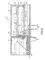
- Figure 1 is a front perspective view of a PCB board mountable converter module that uses a wired Ethernet connection.
- Figure 2 is a front view of the module of Figure 1.
- Figure 3 is a side, partially cut-away view of the module of Figure 1.
- Figure 4 is a side cross-sectional view of the module of Figure 1.
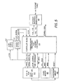
- FIG. 5 is a block diagram of the electrical component circuitry for the module of
- Figure 6 is a pin input and output diagram of the module of Figure 1, or a wireless embodiment..
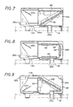
- Figure 7 is a side, partially cut-away view of an alternative embodiment of a module, having horizontal and angles circuit boards.
- Figure 8 is a side, partially cut-away view of an alternative embodiment of a module, having circuit boards placed on a common flexible substrate.
- Figure 9 is a side, partially cut-away view of an alternative embodiment of a module, having vertical and angled circuit boards.
- Figure 10 is an alternative embodiment of a connector, having an interior chamber located beneath the connector port.
- Figure 11A is a perspective cutaway view of a commercial WiPort TM module.
- Figure 11B is a bottom perspective view of a commercial WiPort TM module.
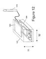
- Figure 12 is a perspective cutaway view of a module in which a serial to wireless Ethernet capability is embodied in a housing having an approximate cross-sectional size and shape of an RJ-45 connector.
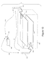
- Figure 13 is a cutaway view of a device having a board having two wireless modules.
- module 10 comprises a generally rectangular housing 12.
- the front of the housing includes an open cavity 14.
- a metal Faraday shield covers the top, sides and back of the housing and provides for electromagnetic-radiation (EMR) protection.
- the module 10 additionally includes spring biased grounding tabs 16 that connect the Faraday shield to chassis (earth) ground by contacting the enclosure in which the connector is mounted.
- an array of leads 20 for electrically interconnecting the module 10 to a printed circuit board (PCB) 18.
- PCB printed circuit board
- the cavity 14 of the housing 12 incorporates a planar array of parallel electrical contacts 22 to provide the necessary electrical contacts to form a connector port within the cavity 14.
- the cavity 14 is sized and dimensioned and the contacts 22 are placed within the cavity to compliment a mating plug (not shown).
- the sized cavity 14 along with the contacts 22 form a standard RJ-45 connector jack.
- the jack contacts 22 are spring biased for engagement with a mating plug (not shown).
- the housing 12 is formed of molded plastic or other suitable material used in the art, covered by a Faraday shield having a front wall 24, a rear wall 26, a top wall 28, a bottom wall 30, and sidewalls 32 and 34.
- a Faraday shield having a front wall 24, a rear wall 26, a top wall 28, a bottom wall 30, and sidewalls 32 and 34.
- the references herein to "top”, “bottom”, and “sides” are made for ease of explanation relative to the drawing.
- Alternative embodiments eliminate the plastic, and the housing material is chosen to perform the Faraday shielding function without separate components, for example by using conductive metal.
- the module 10 can be oriented in a multitude of ways on a product, thereby accommodating engineering requirements of specific placements.
- the front wall 24 includes LEDs 36 and 38.
- the LEDs provide visual status and fault information for various functions of the serial-to-Ethernet conversion, such as (but not limited to) Ethernet connection speed, link present/absent, full/half duplex, Ethernet activity, serial port activity, and microcontroller error conditions.
- the housing 12 includes a segregated interior chamber 40.
- a first PCB 42 is disposed within the interior chamber 40 generally horizontal and parallel relative to the bottom wall 30.
- the first PCB 42 is soldered (or otherwise electrically connected) to the contact interface 44, which is mounted in a plastic insert.
- the completed insert assembly slides and snaps into the main housing 12.
- the contact interface pins 44 are formed such that their ends become the wiper contacts 22.
- the contact interface 44 additionally provides structural support to the first PCB 42.
- a second PCB 50 is also placed within the interior chamber 40, positioned generally horizontal and in general parallel relation to the bottom wall 30.
- the third PCB 50 is soldered (or otherwise electrically connected) to the array of leads 54, which are formed such that their ends become the input/output pins 20 (more specifically, these pins 20 connect power and ground, reset, serial data input and output, handshake and flow control lines, and PIO lines) that connect to the user's PCB 20.
- the array of leads 54 are mounted in a plastic insert. After the third PCB 50 is soldered (or otherwise connected) to the leads 54, the completed insert assembly slides and snaps into the main housing 12.
- a third PCB 48 is placed within the interior chamber 40 in a generally vertical orientation, and is generally perpendicular to the other PCBs 42 and 50.
- PCB 48 is positioned adjacent the rear wall 26 and is structurally and electrically interconnected to the other PCBs 42 and 50 by the formed pins 49 and 52.
- PCB 48 and formed pins 49 and 52 thus provide the electrical connection between PCBs 42 and 50.
- the LEDs 38 have leads (not shown) that run close to the top of the enclosure 12, and these leads also connect to holes in PCB 48. This provides the electrical connection between the LEDs 38 and the control PCB 50.
- the first, 42, and second PCB 50 collectively incorporate the electronic circuitry component necessary to complete a serial-to-Ethernet conversion of data.
- PCB 42 includes the magnetics portion of the circuitry which can advantageously include isolation transformers, common mode chokes, termination resistors, and a high voltage discharge capacitor (for ESD and voltage surges).
- PCB 48 is used solely for electrical interconnection, but it could also be used for circuitry components if required.
- PCB 50 incorporates all of the electronic circuitry components necessary for the control function of the serial-to-Ethernet conversion.
- the electronic components on board PCB 50 include, but are not limited to, a microprocessor and an Ethernet controller (which can advantageously be combined in an ASIC), nonvolatile memory (flash memory in the present invention), voltage regulator, voltage supervisory circuit, crystals, resistors, capacitors, and ferrite or other surface mount beads.
- the complete assembly is mounted on a PCB that is a part of some device or equipment.
- Serial data and general purpose PIO data flows from the device through the array of leads 20 and is processed by the circuitry collectively incorporated onto PCBs 42, 48 and 50.
- PCB 42 is interconnected to the contacts 22 which mate with a plug (not shown) to effectively transmit Ethernet data thereto.
- Ethernet data can also flow from the Ethernet port through wiper contacts 22, be processed by the circuitry collectively incorporated onto PCBs 42, 48 and 50, and flow out as serial data and general purpose PIO data through lead pins 20 into the external device.
- the control circuitry, magnetic circuitry and LED circuitry can be interchanged among PCBs 42, 48 and 50 and that component can be positioned on one or both sides of each PCB's 42, 48 and 50.
- the controller block 56 handles all of the conversion between serial and Ethernet. This includes processing of the digital (serial) and analog (Ethernet) signals, as well as all of the required code protocol translations.
- the controller block 56 communicates with Ethernet through the Ethernet interface 58, which is described below in greater detail.
- the flash memory 66 stores the software that the controller block 56 uses to perform its functions.
- the supervisory circuit 68 monitors the supply voltage coming in through the PCB 10 pins 64. It resets the controller block if the voltage drops too low, or if a signal from the PCB 10 pins 64 requests a system reset.
- the power filters 60 remove noise from the input supply voltage, and also reduce any noise that might be transmitted from the serial-to-Ethernet converter to the outside world through the voltage supply lines.
- the power supply 62 supplies one or more voltages required by the controller block.
- Serial data is transmitted to and from the controller block through the PCB IO pins 64 to the external device.
- the flow control and handshake lines (connected through PCB IO pins 64) are standard signals used to control the serial data stream.
- the controller block can also communicate with the external device through the PIO lines connecting through the PCB IO pins 64. It is understood that although the components as shown in Figure 5 are specifically identified, all suitable control circuitry that implement the desired functions are also contemplated.
- the outgoing Ethernet signal 70a from the controller 50 passes through the isolation transformer 74, which eliminates any DC coupling problems between Ethernet devices.
- the outgoing signals pass through the common mode choke 78, which reduces spurious emissions (radiated and conducted).
- the outgoing signal connects to the Ethernet cable through contacts 72a of the RJ-45 jack.
- Incoming Ethernet signals enter into the jack through contacts 72c, and pass through a common mode choke 80 that reduces spurious common mode noise that could be conducted into the device.
- the signals pass through the isolation transformer 76, and then to the controller board 50 through pins 52 and 26.
- the center taps 70b and 70c of the isolation transformers 74 and 76 are used to set the appropriate DC bias levels in the transmit and receive circuitry on the controller board 50.
- the alternate module of Figure 7 is structurally similar to the embodiment shown in Figures 1-4, with only the distinctions highlighted below.
- two PCBs 86 and 88 are positioned therein.
- a first PCB 88 is positioned generally horizontal in parallel relation to the bottom wall 30a.
- a second PCB 86 is positioned in angular relation to the PCB 88 to fit within the interior chamber 40a.
- PCB 86 and 88 collectively incorporate the electric circuitry components to complete a serial to Ethernet data conversion.
- PCB 86 is interconnected to a lead array 20a.
- PCB 86 includes all of the control circuitry, with components interconnected to the top side and bottom side of said PCB.
- PCB 86 is interconnected to PCB 88.
- PCB 88 includes the magnetic portion of the circuitry formed on the underside of PCB 86.
- the LEDs 38a and 36a also connect to PCB 86 through leads 14a.
- PCB 88 is interconnected to contacts 22a.
- the alternate module of Figure 8 is also structurally similar to the embodiment as shown in Figures 1-4.
- a common flexible substrate more specifically, a rigid/flexible PCB 90, 92, 94, and 96
- the rigid/flexible PCB 90, 92, 94, and 96 collectively incorporates the electric circuitry components to complete a serial to Ethernet data conversion. Electrical and magnetic components can be mounted on the rigid portions of the PCB 92, 94, and 96. Electrical connections between the rigid portions 92, 94, and 96 are made on the flexible portions 90. Rigid portion 96 is electrically connected to the lead array 20b.
- Control circuitry can be incorporated onto rigid portion 96 and possibly 94, with magnetic circuitry incorporated on rigid portion 92 and possibly 94.
- the LEDs connect to rigid portion 96 through leads 14b.
- Rigid portion 92 is electrically connected to contacts 22. It is additionally contemplated that the control circuitry, magnetic circuitry and LED connections can be interchanged among rigid portions 92, 94 and 96.
- the alternate module of Figure 9 is again structurally similar to the embodiment shown in Figures 1-4.
- the main difference is that two PCBs 98 and 100 are positioned within the interior chamber 40c.
- the first PCB 98 is positioned generally vertically in parallel relation to the rear wall 26.
- a second PCB 100 is positioned in angular relation to the PCB 98 to fit within the interior chamber 40c.
- PCB 98 and 100 collectively incorporate the electric circuitry components to complete a serial-to-Ethernet data conversion.
- PCB 100 is interconnected to a lead array 20c.
- PCB 100 includes all of the control circuitry with components interconnected to the top side and bottom side of said PCB.
- PCB 98 is interconnected to PCB 100.
- PCB 98 includes a magnetic portion of the circuitry.
- PCB 98 is interconnected to contacts 22c.
- PCB 100 is additionally interconnected to LEDs 38c and 36c.
- the alternate module of Figure 10 once again includes a connector port that is structurally similar to the embodiment shown in Figures 1-4, but which does not include an interior chamber located behind the port.
- the interior chamber 102 is located beneath the port cavity 14d.
- at least one PCB is positioned therein which incorporates the electric circuitry components to complete a serial-to-Ethernet data conversion.
- the serial-to-Ethernet circuitry can be incorporated into the interior chamber 102 in a variety of ways, including those described with respect to the interior chambers of Figures 4 and 7-9.
- the port cavity 14d in any embodiment can be replaced or augmented with a radio antenna, radio antenna connector or remote radio antenna wiring.
- Wireless networking versions of the modules of Figures 1-10 can be implemented by replacing the magnetics with a suitable radio circuitry and power amplifier, receiver, etc. Such substitutions can be implemented without altering the overall design of the module, but is more preferably implemented using structure and electronics as set forth in Figures 11A-C, 12 and 13.
- the partitioning of required circuitry on the interior PCBs within the interior chamber can be accomplished in any suitable manner, it is especially convenient to arrange the Ethernet radio components on a single PCB 1106, with remaining control and supervision circuitry on PCB 1107.
- the board or boards can be positioned in any practical relationship with respect to each other and with respect to the housing.
- the first PCB 1106 includes antenna connector 1103 and can advantageously provide for a second (diversity) antenna or connector 1104.
- the second PCB 1107 can alternatively replace leads 54 by including mating connector 1101 for electrical board mounting.
- Connector 1101 comprises three or more pins 1113 and can include any or all of serial data pins, handshaking and flow control pins, GPIO pins and pins supporting other serial or parallel protocols as desired.
- PCB 1107 can also incorporate all of the electronic circuitry components necessary for the control function of the serial-to-Ethernet conversion. There are, of course, a great diversity of pins in use, and additional pin configurations will undoubtedly be utilized in the future. With that caveat in mind, connector 1101 is to be interpreted euphemistically to include all manner of pin cross sections, square, rectangular, flattened, etc, and all manner of configurations of pins.
- novel wireless modules as set forth herein may attach a conventional RJ-45 jack incorporating magnetics, because the Ethernet wires may be brought out of connector 1101.
- data communication may take place between and among any of the provided interfaces and protocols, including serial, wireless and wired Ethernet interfaces.
- the electronic components on PCB 1107 can include, but are not limited to, a microprocessor and an Ethernet controller (combined in an ASIC for the present invention), at least 256KB of memory that stores an operating system and environment and at least 2MB of nonvolatile memory that stores at least one web page (flash memory in the present invention), voltage regulator, voltage supervisory circuit, crystals, resistors, capacitors, and ferrite beads (surface mount beads in the present invention).
- a current commercial embodiment according to Figures 11A and 11B has the following specifications: Wireless Specifications Network Standard IEEE 802.11b Frequency Range 2.412-2.484 GHz Output Power 14dBm +/- 1.0 dBm Antenna Connector 1, no diversity supported.
- Radio # of Selectable Channels 14 Channels Modulation DSSS, DBPSK, DQPSK, CCK Antenna Connector 1 Security WEP 64/128, TKIP Maximum Receive Level -10dBm (with PER ⁇ 8%) • -82dBm for 11 Mbps Receiver Sensitivity • -87dBm for 5.5Mbps • -89dBm for 2 0Mb • -93dBm for 1.0Mbps WLAN Power and Link LED Current Max: 4mA Other Specifications CPU, Memory Lantronix DSTni-EX 186 CPU, 256 KB zero wait state SRAM 2048 KB Flash or 4096 KB Flash, 16 KB Boot ROM, 1024 KB SRAM Firmware Upgradeable via TFTP and serial port Reset Circuit Reset In is low active.
- MILARRS refers to the following: Monitoring the state of the device for an administrator; Inventory the devices sub-systems, components, or assets; Logging data or events generated by the device; Alerting an administrator of device state or taking action based on defined rules; Recovering the device if it fails or shuts down; Reporting device information or diagnostics to an administrator; and Securing the device and its assets from threats and risks. Additional details regarding the acronym and implementation are set forth in US 11/031643, filed January 7, 2005 .
- the housing 1201 can represent a similar form factor in height and width to conventional passive RJ45 jacks, where height can be in a range of 12 to 14 mm or more and width in a range of 15 to 24mm or more. In a particularly preferred embodiment, height is approximately 13 mm and width is approximately 16mm.
- the translation circuitry can be split among multiple components disposed on PCB 1203 and PCB 1204, or even across other boards as can be necessary or desirable.
- antenna 1205 a second (diversity) antenna can be provided.
- a device 1301 has one or more component boards 1304, 1305, upon which are mounted two modules 1303 and 1306.
- the 1303 module is directly connected to the board 1304 using soldered pins.
- the 1306 module can be mounted on the board 1305 using an intermediate coupling.
- the modules 1303 and 1306 are able to talk with one another and with a device 1302 in the outside world wirelessly using their respective antenna 1307, 1312 and 1308 via the conventional device to device paths 1309 and 1310 but also by the unconventional path 131 connecting two points within the same device wirelessly.
- Path 1311 can be desirable for providing routing flexibility, architectural generality, and digital signal integrity including secure encryption or physical convenience.
- the device of Figure 13 is drawn generically, and is intended to represent any suitable device, including but not limited to Information Technology equipment, electronic communications equipment, networked device appliances or remote management modules, medical or security equipment, industrial monitoring, sensing or control equipment, digital storage or processing devices and equipment and consumer audio or video entertainment components or devices.
- Such contemplated devices vary tremendously, and for example, can range in size from chip scale components to rack mounted enclosures to room or building sized systems, and in intelligence from basic GPIO signal communication to complete protocol bridging functions or inclusion of management functions such as provision of one or all of MILARRS functions, web services, gateway functions, database access or search, or any other function enabled by wireless local or worldwide network connection.
Applications Claiming Priority (1)
| Application Number | Priority Date | Filing Date | Title |
|---|---|---|---|
| US11/084,342 US7309260B2 (en) | 2002-04-15 | 2005-03-17 | Wireless communication module |
Publications (3)
| Publication Number | Publication Date |
|---|---|
| EP1703698A2 true EP1703698A2 (fr) | 2006-09-20 |
| EP1703698A3 EP1703698A3 (fr) | 2012-02-22 |
| EP1703698B1 EP1703698B1 (fr) | 2014-01-22 |
Family
ID=36617301
Family Applications (1)
| Application Number | Title | Priority Date | Filing Date |
|---|---|---|---|
| EP06251431.0A Active EP1703698B1 (fr) | 2005-03-17 | 2006-03-17 | Port de communication sans fil |
Country Status (6)
| Country | Link |
|---|---|
| US (1) | US7309260B2 (fr) |
| EP (1) | EP1703698B1 (fr) |
| JP (2) | JP5239096B2 (fr) |
| CA (2) | CA2600804C (fr) |
| TW (1) | TWI355122B (fr) |
| WO (1) | WO2006099627A1 (fr) |
Cited By (2)
| Publication number | Priority date | Publication date | Assignee | Title |
|---|---|---|---|---|
| DE202008003012U1 (de) | 2008-03-03 | 2008-07-24 | Apator S.A. | Gehäuse eines kabellosen Kommunikationssports |
| CN101604809A (zh) * | 2008-06-10 | 2009-12-16 | 泰科电子Amp有限责任公司 | 插入式连接器和用于将导电体连接到插入式连接器的方法 |
Families Citing this family (58)
| Publication number | Priority date | Publication date | Assignee | Title |
|---|---|---|---|---|
| US7698405B2 (en) * | 2005-01-07 | 2010-04-13 | Lantronix, Inc. | MILARRS systems and methods |
| US20060209886A1 (en) * | 2005-03-04 | 2006-09-21 | Rad Data Communications, Ltd. | Small form-factor device implementing protocol conversion |
| US7396257B2 (en) * | 2005-05-26 | 2008-07-08 | Itt Manufacturing Enterprises, Inc. | Computer input/output (I/O) connector assembly having a security circuit disposed therein |
| US8488792B2 (en) * | 2005-10-26 | 2013-07-16 | Hewlett-Packard Development Company, L.P. | Wireless communications validation system and method |
| US20070173077A1 (en) * | 2006-01-24 | 2007-07-26 | Hwa Yao Technologies Co., Ltd. | Universal serial bus (usb) network adapter connectable to external antenna |
| US7974577B2 (en) * | 2006-04-11 | 2011-07-05 | Tazzle, Inc. | Devices and systems for improved wireless communication |
| AU2007291879B2 (en) * | 2006-09-01 | 2011-07-28 | Reichle & De-Massari Ag | Adapter and plug-in connection system |
| US8332567B2 (en) | 2006-09-19 | 2012-12-11 | Fisher-Rosemount Systems, Inc. | Apparatus and methods to communicatively couple field devices to controllers in a process control system |
| US9411769B2 (en) | 2006-09-19 | 2016-08-09 | Fisher-Rosemount Systems, Inc. | Apparatus and methods to communicatively couple field devices to controllers in a process control system |
| US7724204B2 (en) * | 2006-10-02 | 2010-05-25 | Pulse Engineering, Inc. | Connector antenna apparatus and methods |
| EP2087440A2 (fr) * | 2006-11-19 | 2009-08-12 | Rmax, LLC | Ordinateur basé sur internet pour des utilisateurs clients légers et mobiles |
| JP4449990B2 (ja) * | 2007-02-22 | 2010-04-14 | ソニー株式会社 | 接続構造及び信号伝送ケーブル |
| US20080274646A1 (en) * | 2007-05-04 | 2008-11-06 | Schneider Electric Gmbh | Ethernet connectors |
| US7699174B2 (en) * | 2007-06-26 | 2010-04-20 | Tyco Electronics Corporation | Electrical connector interfaced with conductive ink on a cardboard substrate |
| US8890877B2 (en) * | 2008-02-28 | 2014-11-18 | Standard Microsystems Corporation | Updating firmware in a display device using a serial bus |
| US7850466B2 (en) * | 2008-06-23 | 2010-12-14 | Tyco Electronics Corporation | Through board inverted connector |
| US7704082B2 (en) * | 2008-06-23 | 2010-04-27 | Tyco Electronics Corporation | Through board inverted connector |
| US7789713B2 (en) * | 2008-06-24 | 2010-09-07 | Tibbo Technology, Inc. | Connector jack with reduced host PCB footprint, assembly thereof and fabrication method of the same |
| US7537491B1 (en) * | 2008-07-10 | 2009-05-26 | Michael Feldman | Interface unit |
| US7704098B2 (en) | 2008-07-22 | 2010-04-27 | Amphenol Corporation | Registered jack with enhanced EMI protection |
| US7695309B2 (en) * | 2008-08-26 | 2010-04-13 | Tyco Electronics Corporation | Sensor strip for a connectivity management system |
| US9083548B2 (en) * | 2008-09-23 | 2015-07-14 | Fisher-Rosemount Systems, Inc. | Apparatus and methods to communicatively couple field devices to controllers in a process control system |
| TW201021305A (en) * | 2008-11-28 | 2010-06-01 | Delta Electronics Inc | Connecter |
| TWI320248B (en) * | 2008-12-02 | 2010-02-01 | Rj45 joint device with key structure to change definition of pin | |
| US8977851B2 (en) * | 2009-01-21 | 2015-03-10 | Fisher-Rosemount Systems, Inc. | Removable security modules and related methods |
| US7699663B1 (en) * | 2009-07-29 | 2010-04-20 | Hon Hai Precision Ind. Co., Ltd. | Electrical connector with improved grounding contact |
| US7892031B1 (en) * | 2009-07-30 | 2011-02-22 | Tyco Electronics Corporation | Quick insertion lamp assembly |
| CN102725922B (zh) | 2009-11-06 | 2017-03-29 | 莫列斯公司 | 电连接器、多层电路元件以及滤波模块 |
| CN102696154B (zh) * | 2009-11-06 | 2015-07-29 | 莫列斯公司 | 连接器 |
| TWI416981B (zh) * | 2009-12-11 | 2013-11-21 | Equaline Corp | 混合式服務裝置暨系統 |
| US10305910B2 (en) | 2010-01-15 | 2019-05-28 | Apple Inc. | Accessing specialized fileserver |
| US8577579B2 (en) * | 2010-02-01 | 2013-11-05 | Bendix Commercial Vehicle Systems Llc | Engine control request from adaptive control with braking controller |
| DE202010003457U1 (de) * | 2010-03-11 | 2010-06-02 | Rosenberger Hochfrequenztechnik Gmbh & Co. Kg | Leiterplattensteckverbinder |
| TWM396531U (en) * | 2010-08-16 | 2011-01-11 | Tuton Technology Co Ltd | Improved connector structure with protection device |
| US20120044655A1 (en) * | 2010-08-20 | 2012-02-23 | George Nichols | GPS-Timing Module |
| US8029320B1 (en) * | 2010-11-15 | 2011-10-04 | Intel Corporation | Integrated module including physical layer network device, receptacle and physical layer isolation module |
| US8907774B2 (en) | 2011-03-01 | 2014-12-09 | Bendix Commercial Vehicle Systems Llc | System and method for monitoring tire condition |
| US8606461B2 (en) | 2011-12-09 | 2013-12-10 | Bendix Commercial Vehicle Systems Llc | System and method for monitoring tire status |
| US9594536B2 (en) * | 2011-12-29 | 2017-03-14 | Ati Technologies Ulc | Method and apparatus for electronic device communication |
| US8920197B2 (en) | 2012-03-14 | 2014-12-30 | Apple Inc. | Connector receptacle with ground contact having split rear extensions |
| CN103428903B (zh) * | 2012-05-16 | 2016-12-21 | 华为终端有限公司 | 无线通信设备和制造无线通信设备的方法 |
| US9011176B2 (en) * | 2012-06-09 | 2015-04-21 | Apple Inc. | ESD path for connector receptacle |
| DE102012022167A1 (de) * | 2012-11-12 | 2014-05-15 | Yamaichi Electronics Deutschland Gmbh | Verbinder und Verwendung |
| FR2998128B1 (fr) * | 2012-11-13 | 2016-10-07 | Microturbo | Calculateur de turbo-machine d'aeronef |
| CN103915731B (zh) * | 2013-01-09 | 2016-06-08 | 富士康(昆山)电脑接插件有限公司 | 电连接器 |
| US9067466B2 (en) | 2013-01-30 | 2015-06-30 | Bendix Commercial Vehicle Systems Llc | Diversity antenna |
| CN104103968A (zh) * | 2013-04-15 | 2014-10-15 | 富士康(昆山)电脑接插件有限公司 | 电连接器 |
| CN104716492B (zh) * | 2013-12-13 | 2017-05-24 | 富士康(昆山)电脑接插件有限公司 | 电连接器 |
| CN204424561U (zh) * | 2015-02-13 | 2015-06-24 | 东莞建冠塑胶电子有限公司 | Rj45模块化分离式组装结构 |
| US9804834B1 (en) | 2016-04-19 | 2017-10-31 | Dropbox, Inc. | Automatically updating a hybrid application |
| EP3258547A1 (fr) * | 2016-06-17 | 2017-12-20 | Tyco Electronics Componentes Electromecanicos Lda | Connecteur électrique de véhicule automobile présentant une surface de montage |
| FR3060826B1 (fr) * | 2016-12-19 | 2019-05-24 | Moteurs Leroy-Somer | Regulateur numerique de tension d'alternateur a technologie nfc |
| USD840341S1 (en) | 2017-06-20 | 2019-02-12 | Amphenol Corporation | Cable connector |
| USD839193S1 (en) | 2017-06-20 | 2019-01-29 | Amphenol Corporation | Cable connector |
| US10186804B2 (en) | 2017-06-20 | 2019-01-22 | Amphenol Corporation | Cable connector with backshell locking |
| CN108023897B (zh) * | 2018-01-05 | 2024-04-09 | 深圳有电物联科技有限公司 | 通信端口及具有所述通信端口的电子设备 |
| CN111727609A (zh) * | 2018-02-22 | 2020-09-29 | 铂特工业自动化有限公司 | 集成通信单元 |
| US11937393B2 (en) | 2021-11-16 | 2024-03-19 | Arinc Incorporated | Circuit board assembly and system for communication to an access point of an avionics network |
Citations (8)
| Publication number | Priority date | Publication date | Assignee | Title |
|---|---|---|---|---|
| GB2360608A (en) * | 1999-10-22 | 2001-09-26 | Roke Manor Research | A fully integrated Web activated control and monitoring device |
| US20020075816A1 (en) * | 2000-12-12 | 2002-06-20 | Beckwith Robert W. | Wireless transceivers using a simplified Prism II system |
| WO2003019915A1 (fr) * | 2001-08-24 | 2003-03-06 | Nokia Corporation | Module de serveur enfichable pour telecommande sans fil des dispositifs |
| US20030139821A1 (en) * | 1997-09-10 | 2003-07-24 | Papadopoulos A. Dean | System and method for interfacing with a controller |
| US6633583B1 (en) * | 1998-12-18 | 2003-10-14 | Intel Corporation | Wireless universal serial bus receiver |
| US20030194908A1 (en) * | 2002-04-15 | 2003-10-16 | Brown Curtis D. | Compact serial -to ethernet conversion port |
| EP1465420A2 (fr) * | 2003-04-03 | 2004-10-06 | Eastman Kodak Company | Dispositif d'emmagasinage compact sans fil. |
| WO2006077294A1 (fr) * | 2005-01-20 | 2006-07-27 | Telecom Design | Dispositif interface a module extractible |
Family Cites Families (9)
| Publication number | Priority date | Publication date | Assignee | Title |
|---|---|---|---|---|
| JPH1127277A (ja) * | 1997-07-01 | 1999-01-29 | Mitsumi Electric Co Ltd | 無線通信装置 |
| US20020090001A1 (en) * | 1999-01-25 | 2002-07-11 | Beckwith Robert W. | Wireless communications hub with protocol conversion |
| DE19928998B4 (de) * | 1999-06-24 | 2005-07-14 | Siemens Ag | Elektronische Schaltungsanordnung zur Erzeugung einer Sendefrequenz |
| JP2001285298A (ja) * | 2000-03-29 | 2001-10-12 | Hitachi Kokusai Electric Inc | 無線データ通信システム |
| US6603394B2 (en) * | 2000-12-08 | 2003-08-05 | Spx Corporation | Multi-protocol wireless communication module |
| US20030031138A1 (en) * | 2000-12-12 | 2003-02-13 | Beckwith Robert W. | Wireless transceivers using a simplified prism II system |
| US6636749B2 (en) * | 2001-06-25 | 2003-10-21 | At&T Wireless Services, Inc. | Method and apparatus for providing power and wireless protocol capability to a wireless device, such as a wireless phone |
| US6875051B2 (en) * | 2003-05-27 | 2005-04-05 | Design Research And Development Corp. | Electrical power distribution device |
| US7025627B2 (en) * | 2004-01-27 | 2006-04-11 | Leap Technologies, Inc. | Apparatus for connecting and organizing cords and cables |
-
2005
- 2005-03-17 US US11/084,342 patent/US7309260B2/en not_active Expired - Lifetime
-
2006
- 2006-03-17 EP EP06251431.0A patent/EP1703698B1/fr active Active
- 2006-03-17 JP JP2008502145A patent/JP5239096B2/ja active Active
- 2006-03-17 CA CA2600804A patent/CA2600804C/fr active Active
- 2006-03-17 WO PCT/US2006/010061 patent/WO2006099627A1/fr active Application Filing
- 2006-03-17 TW TW095109129A patent/TWI355122B/zh active
- 2006-03-17 CA CA2753406A patent/CA2753406C/fr active Active
-
2012
- 2012-12-04 JP JP2012265700A patent/JP5689109B2/ja active Active
Patent Citations (8)
| Publication number | Priority date | Publication date | Assignee | Title |
|---|---|---|---|---|
| US20030139821A1 (en) * | 1997-09-10 | 2003-07-24 | Papadopoulos A. Dean | System and method for interfacing with a controller |
| US6633583B1 (en) * | 1998-12-18 | 2003-10-14 | Intel Corporation | Wireless universal serial bus receiver |
| GB2360608A (en) * | 1999-10-22 | 2001-09-26 | Roke Manor Research | A fully integrated Web activated control and monitoring device |
| US20020075816A1 (en) * | 2000-12-12 | 2002-06-20 | Beckwith Robert W. | Wireless transceivers using a simplified Prism II system |
| WO2003019915A1 (fr) * | 2001-08-24 | 2003-03-06 | Nokia Corporation | Module de serveur enfichable pour telecommande sans fil des dispositifs |
| US20030194908A1 (en) * | 2002-04-15 | 2003-10-16 | Brown Curtis D. | Compact serial -to ethernet conversion port |
| EP1465420A2 (fr) * | 2003-04-03 | 2004-10-06 | Eastman Kodak Company | Dispositif d'emmagasinage compact sans fil. |
| WO2006077294A1 (fr) * | 2005-01-20 | 2006-07-27 | Telecom Design | Dispositif interface a module extractible |
Non-Patent Citations (1)
| Title |
|---|
| FERRO E ET AL: "Bluetooth and wi-fi wireless protocols: a survey and a comparison", IEEE WIRELESS COMMUNICATIONS, IEEE SERVICE CENTER, PISCATAWAY, NJ, US, vol. 12, no. 1, 1 February 2005 (2005-02-01), pages 12-26, XP011127716, ISSN: 1536-1284, DOI: 10.1109/MWC.2005.1404569 * |
Cited By (4)
| Publication number | Priority date | Publication date | Assignee | Title |
|---|---|---|---|---|
| DE202008003012U1 (de) | 2008-03-03 | 2008-07-24 | Apator S.A. | Gehäuse eines kabellosen Kommunikationssports |
| EP2099270A2 (fr) | 2008-03-03 | 2009-09-09 | Apator S.A. | Boîtier d'un port de communication sans fil |
| CN101604809A (zh) * | 2008-06-10 | 2009-12-16 | 泰科电子Amp有限责任公司 | 插入式连接器和用于将导电体连接到插入式连接器的方法 |
| CN101604809B (zh) * | 2008-06-10 | 2013-07-10 | 泰科电子Amp有限责任公司 | 插入式连接器和用于将导电体连接到插入式连接器的方法 |
Also Published As
| Publication number | Publication date |
|---|---|
| JP5239096B2 (ja) | 2013-07-17 |
| WO2006099627A1 (fr) | 2006-09-21 |
| EP1703698A3 (fr) | 2012-02-22 |
| CA2600804C (fr) | 2012-06-05 |
| US20050181643A1 (en) | 2005-08-18 |
| TWI355122B (en) | 2011-12-21 |
| CA2600804A1 (fr) | 2006-09-21 |
| US7309260B2 (en) | 2007-12-18 |
| EP1703698B1 (fr) | 2014-01-22 |
| JP2013081219A (ja) | 2013-05-02 |
| JP2008533931A (ja) | 2008-08-21 |
| CA2753406C (fr) | 2014-02-11 |
| TW200642206A (en) | 2006-12-01 |
| JP5689109B2 (ja) | 2015-03-25 |
| CA2753406A1 (fr) | 2006-09-21 |
Similar Documents
| Publication | Publication Date | Title |
|---|---|---|
| EP1703698B1 (fr) | Port de communication sans fil | |
| US6881096B2 (en) | Compact serial-to-ethernet conversion port | |
| US8924518B2 (en) | Communication protocol converter and method of protocol conversion | |
| US6174205B1 (en) | Communication card extension and adapter port | |
| US8843678B2 (en) | Method and system for a configurable connector for ethernet applications | |
| US8092258B2 (en) | Modular outlet | |
| US20050197012A1 (en) | Local area network connector for use as a separator | |
| EP3342114B1 (fr) | Noeud de communication à interface de plan numérique | |
| US20030169205A1 (en) | Modular printed antenna | |
| US7189119B2 (en) | Adapter having transient suppression protection | |
| WO2008090341A2 (fr) | Adaptateur de prise électrique | |
| US9559476B2 (en) | ARJ45 to RJ45 adapter |
Legal Events
| Date | Code | Title | Description |
|---|---|---|---|
| PUAI | Public reference made under article 153(3) epc to a published international application that has entered the european phase |
Free format text: ORIGINAL CODE: 0009012 |
|
| 17P | Request for examination filed |
Effective date: 20060324 |
|
| AK | Designated contracting states |
Kind code of ref document: A2 Designated state(s): AT BE BG CH CY CZ DE DK EE ES FI FR GB GR HU IE IS IT LI LT LU LV MC NL PL PT RO SE SI SK TR |
|
| AX | Request for extension of the european patent |
Extension state: AL BA HR MK YU |
|
| RIC1 | Information provided on ipc code assigned before grant |
Ipc: H04L 29/06 20060101AFI20111010BHEP |
|
| PUAL | Search report despatched |
Free format text: ORIGINAL CODE: 0009013 |
|
| AK | Designated contracting states |
Kind code of ref document: A3 Designated state(s): AT BE BG CH CY CZ DE DK EE ES FI FR GB GR HU IE IS IT LI LT LU LV MC NL PL PT RO SE SI SK TR |
|
| AX | Request for extension of the european patent |
Extension state: AL BA HR MK YU |
|
| RIC1 | Information provided on ipc code assigned before grant |
Ipc: H04L 29/06 20060101AFI20120113BHEP |
|
| AKX | Designation fees paid |
Designated state(s): AT BE BG CH CY CZ DE DK EE ES FI FR GB GR HU IE IS IT LI LT LU LV MC NL PL PT RO SE SI SK TR |
|
| 17Q | First examination report despatched |
Effective date: 20130219 |
|
| GRAP | Despatch of communication of intention to grant a patent |
Free format text: ORIGINAL CODE: EPIDOSNIGR1 |
|
| INTG | Intention to grant announced |
Effective date: 20130729 |
|
| GRAS | Grant fee paid |
Free format text: ORIGINAL CODE: EPIDOSNIGR3 |
|
| GRAA | (expected) grant |
Free format text: ORIGINAL CODE: 0009210 |
|
| AK | Designated contracting states |
Kind code of ref document: B1 Designated state(s): AT BE BG CH CY CZ DE DK EE ES FI FR GB GR HU IE IS IT LI LT LU LV MC NL PL PT RO SE SI SK TR |
|
| REG | Reference to a national code |
Ref country code: GB Ref legal event code: FG4D |
|
| REG | Reference to a national code |
Ref country code: CH Ref legal event code: EP |
|
| REG | Reference to a national code |
Ref country code: AT Ref legal event code: REF Ref document number: 651223 Country of ref document: AT Kind code of ref document: T Effective date: 20140215 |
|
| REG | Reference to a national code |
Ref country code: IE Ref legal event code: FG4D |
|
| REG | Reference to a national code |
Ref country code: DE Ref legal event code: R096 Ref document number: 602006040147 Country of ref document: DE Effective date: 20140306 |
|
| REG | Reference to a national code |
Ref country code: NL Ref legal event code: VDEP Effective date: 20140122 |
|
| REG | Reference to a national code |
Ref country code: AT Ref legal event code: MK05 Ref document number: 651223 Country of ref document: AT Kind code of ref document: T Effective date: 20140122 |
|
| REG | Reference to a national code |
Ref country code: LT Ref legal event code: MG4D |
|
| PG25 | Lapsed in a contracting state [announced via postgrant information from national office to epo] |
Ref country code: IS Free format text: LAPSE BECAUSE OF FAILURE TO SUBMIT A TRANSLATION OF THE DESCRIPTION OR TO PAY THE FEE WITHIN THE PRESCRIBED TIME-LIMIT Effective date: 20140522 Ref country code: LT Free format text: LAPSE BECAUSE OF FAILURE TO SUBMIT A TRANSLATION OF THE DESCRIPTION OR TO PAY THE FEE WITHIN THE PRESCRIBED TIME-LIMIT Effective date: 20140122 |
|
| PG25 | Lapsed in a contracting state [announced via postgrant information from national office to epo] |
Ref country code: SE Free format text: LAPSE BECAUSE OF FAILURE TO SUBMIT A TRANSLATION OF THE DESCRIPTION OR TO PAY THE FEE WITHIN THE PRESCRIBED TIME-LIMIT Effective date: 20140122 Ref country code: CY Free format text: LAPSE BECAUSE OF FAILURE TO SUBMIT A TRANSLATION OF THE DESCRIPTION OR TO PAY THE FEE WITHIN THE PRESCRIBED TIME-LIMIT Effective date: 20140122 Ref country code: AT Free format text: LAPSE BECAUSE OF FAILURE TO SUBMIT A TRANSLATION OF THE DESCRIPTION OR TO PAY THE FEE WITHIN THE PRESCRIBED TIME-LIMIT Effective date: 20140122 Ref country code: FI Free format text: LAPSE BECAUSE OF FAILURE TO SUBMIT A TRANSLATION OF THE DESCRIPTION OR TO PAY THE FEE WITHIN THE PRESCRIBED TIME-LIMIT Effective date: 20140122 Ref country code: ES Free format text: LAPSE BECAUSE OF FAILURE TO SUBMIT A TRANSLATION OF THE DESCRIPTION OR TO PAY THE FEE WITHIN THE PRESCRIBED TIME-LIMIT Effective date: 20140122 Ref country code: NL Free format text: LAPSE BECAUSE OF FAILURE TO SUBMIT A TRANSLATION OF THE DESCRIPTION OR TO PAY THE FEE WITHIN THE PRESCRIBED TIME-LIMIT Effective date: 20140122 Ref country code: PT Free format text: LAPSE BECAUSE OF FAILURE TO SUBMIT A TRANSLATION OF THE DESCRIPTION OR TO PAY THE FEE WITHIN THE PRESCRIBED TIME-LIMIT Effective date: 20140522 |
|
| PG25 | Lapsed in a contracting state [announced via postgrant information from national office to epo] |
Ref country code: LV Free format text: LAPSE BECAUSE OF FAILURE TO SUBMIT A TRANSLATION OF THE DESCRIPTION OR TO PAY THE FEE WITHIN THE PRESCRIBED TIME-LIMIT Effective date: 20140122 Ref country code: BE Free format text: LAPSE BECAUSE OF FAILURE TO SUBMIT A TRANSLATION OF THE DESCRIPTION OR TO PAY THE FEE WITHIN THE PRESCRIBED TIME-LIMIT Effective date: 20140122 |
|
| REG | Reference to a national code |
Ref country code: DE Ref legal event code: R097 Ref document number: 602006040147 Country of ref document: DE |
|
| PG25 | Lapsed in a contracting state [announced via postgrant information from national office to epo] |
Ref country code: DK Free format text: LAPSE BECAUSE OF FAILURE TO SUBMIT A TRANSLATION OF THE DESCRIPTION OR TO PAY THE FEE WITHIN THE PRESCRIBED TIME-LIMIT Effective date: 20140122 Ref country code: LU Free format text: LAPSE BECAUSE OF FAILURE TO SUBMIT A TRANSLATION OF THE DESCRIPTION OR TO PAY THE FEE WITHIN THE PRESCRIBED TIME-LIMIT Effective date: 20140317 Ref country code: RO Free format text: LAPSE BECAUSE OF FAILURE TO SUBMIT A TRANSLATION OF THE DESCRIPTION OR TO PAY THE FEE WITHIN THE PRESCRIBED TIME-LIMIT Effective date: 20140122 Ref country code: CZ Free format text: LAPSE BECAUSE OF FAILURE TO SUBMIT A TRANSLATION OF THE DESCRIPTION OR TO PAY THE FEE WITHIN THE PRESCRIBED TIME-LIMIT Effective date: 20140122 Ref country code: EE Free format text: LAPSE BECAUSE OF FAILURE TO SUBMIT A TRANSLATION OF THE DESCRIPTION OR TO PAY THE FEE WITHIN THE PRESCRIBED TIME-LIMIT Effective date: 20140122 |
|
| REG | Reference to a national code |
Ref country code: CH Ref legal event code: PL |
|
| PG25 | Lapsed in a contracting state [announced via postgrant information from national office to epo] |
Ref country code: SK Free format text: LAPSE BECAUSE OF FAILURE TO SUBMIT A TRANSLATION OF THE DESCRIPTION OR TO PAY THE FEE WITHIN THE PRESCRIBED TIME-LIMIT Effective date: 20140122 Ref country code: PL Free format text: LAPSE BECAUSE OF FAILURE TO SUBMIT A TRANSLATION OF THE DESCRIPTION OR TO PAY THE FEE WITHIN THE PRESCRIBED TIME-LIMIT Effective date: 20140122 |
|
| PLBE | No opposition filed within time limit |
Free format text: ORIGINAL CODE: 0009261 |
|
| STAA | Information on the status of an ep patent application or granted ep patent |
Free format text: STATUS: NO OPPOSITION FILED WITHIN TIME LIMIT |
|
| 26N | No opposition filed |
Effective date: 20141023 |
|
| REG | Reference to a national code |
Ref country code: IE Ref legal event code: MM4A |
|
| PG25 | Lapsed in a contracting state [announced via postgrant information from national office to epo] |
Ref country code: IE Free format text: LAPSE BECAUSE OF NON-PAYMENT OF DUE FEES Effective date: 20140317 Ref country code: CH Free format text: LAPSE BECAUSE OF NON-PAYMENT OF DUE FEES Effective date: 20140331 Ref country code: LI Free format text: LAPSE BECAUSE OF NON-PAYMENT OF DUE FEES Effective date: 20140331 |
|
| REG | Reference to a national code |
Ref country code: DE Ref legal event code: R097 Ref document number: 602006040147 Country of ref document: DE Effective date: 20141023 |
|
| PG25 | Lapsed in a contracting state [announced via postgrant information from national office to epo] |
Ref country code: SI Free format text: LAPSE BECAUSE OF FAILURE TO SUBMIT A TRANSLATION OF THE DESCRIPTION OR TO PAY THE FEE WITHIN THE PRESCRIBED TIME-LIMIT Effective date: 20140122 |
|
| REG | Reference to a national code |
Ref country code: FR Ref legal event code: PLFP Year of fee payment: 11 |
|
| PG25 | Lapsed in a contracting state [announced via postgrant information from national office to epo] |
Ref country code: BG Free format text: LAPSE BECAUSE OF FAILURE TO SUBMIT A TRANSLATION OF THE DESCRIPTION OR TO PAY THE FEE WITHIN THE PRESCRIBED TIME-LIMIT Effective date: 20140122 Ref country code: MC Free format text: LAPSE BECAUSE OF FAILURE TO SUBMIT A TRANSLATION OF THE DESCRIPTION OR TO PAY THE FEE WITHIN THE PRESCRIBED TIME-LIMIT Effective date: 20140122 |
|
| PG25 | Lapsed in a contracting state [announced via postgrant information from national office to epo] |
Ref country code: IT Free format text: LAPSE BECAUSE OF FAILURE TO SUBMIT A TRANSLATION OF THE DESCRIPTION OR TO PAY THE FEE WITHIN THE PRESCRIBED TIME-LIMIT Effective date: 20140122 Ref country code: GR Free format text: LAPSE BECAUSE OF FAILURE TO SUBMIT A TRANSLATION OF THE DESCRIPTION OR TO PAY THE FEE WITHIN THE PRESCRIBED TIME-LIMIT Effective date: 20140423 |
|
| PG25 | Lapsed in a contracting state [announced via postgrant information from national office to epo] |
Ref country code: HU Free format text: LAPSE BECAUSE OF FAILURE TO SUBMIT A TRANSLATION OF THE DESCRIPTION OR TO PAY THE FEE WITHIN THE PRESCRIBED TIME-LIMIT; INVALID AB INITIO Effective date: 20060317 Ref country code: TR Free format text: LAPSE BECAUSE OF FAILURE TO SUBMIT A TRANSLATION OF THE DESCRIPTION OR TO PAY THE FEE WITHIN THE PRESCRIBED TIME-LIMIT Effective date: 20140122 |
|
| REG | Reference to a national code |
Ref country code: FR Ref legal event code: PLFP Year of fee payment: 12 |
|
| REG | Reference to a national code |
Ref country code: FR Ref legal event code: PLFP Year of fee payment: 13 |
|
| REG | Reference to a national code |
Ref country code: DE Ref legal event code: R079 Ref document number: 602006040147 Country of ref document: DE Free format text: PREVIOUS MAIN CLASS: H04L0029060000 Ipc: H04L0065000000 |
|
| PGFP | Annual fee paid to national office [announced via postgrant information from national office to epo] |
Ref country code: FR Payment date: 20230327 Year of fee payment: 18 |
|
| PGFP | Annual fee paid to national office [announced via postgrant information from national office to epo] |
Ref country code: GB Payment date: 20230327 Year of fee payment: 18 Ref country code: DE Payment date: 20230329 Year of fee payment: 18 |