EP1688995A1 - Interposer for decoupling integrated circuits on a circuit board - Google Patents
Interposer for decoupling integrated circuits on a circuit board Download PDFInfo
- Publication number
- EP1688995A1 EP1688995A1 EP05290242A EP05290242A EP1688995A1 EP 1688995 A1 EP1688995 A1 EP 1688995A1 EP 05290242 A EP05290242 A EP 05290242A EP 05290242 A EP05290242 A EP 05290242A EP 1688995 A1 EP1688995 A1 EP 1688995A1
- Authority
- EP
- European Patent Office
- Prior art keywords
- interposer
- metal structures
- circuit board
- microchip
- metal
- Prior art date
- Legal status (The legal status is an assumption and is not a legal conclusion. Google has not performed a legal analysis and makes no representation as to the accuracy of the status listed.)
- Granted
Links
Images

Classifications
-
- H—ELECTRICITY
- H10—SEMICONDUCTOR DEVICES; ELECTRIC SOLID-STATE DEVICES NOT OTHERWISE PROVIDED FOR
- H10W—GENERIC PACKAGES, INTERCONNECTIONS, CONNECTORS OR OTHER CONSTRUCTIONAL DETAILS OF DEVICES COVERED BY CLASS H10
- H10W70/00—Package substrates; Interposers; Redistribution layers [RDL]
- H10W70/60—Insulating or insulated package substrates; Interposers; Redistribution layers
- H10W70/62—Insulating or insulated package substrates; Interposers; Redistribution layers characterised by their interconnections
- H10W70/63—Vias, e.g. via plugs
- H10W70/635—Through-vias
-
- H—ELECTRICITY
- H01—ELECTRIC ELEMENTS
- H01G—CAPACITORS; CAPACITORS, RECTIFIERS, DETECTORS, SWITCHING DEVICES, LIGHT-SENSITIVE OR TEMPERATURE-SENSITIVE DEVICES OF THE ELECTROLYTIC TYPE
- H01G4/00—Fixed capacitors; Processes of their manufacture
- H01G4/002—Details
- H01G4/228—Terminals
- H01G4/232—Terminals electrically connecting two or more layers of a stacked or rolled capacitor
-
- H—ELECTRICITY
- H05—ELECTRIC TECHNIQUES NOT OTHERWISE PROVIDED FOR
- H05K—PRINTED CIRCUITS; CASINGS OR CONSTRUCTIONAL DETAILS OF ELECTRIC APPARATUS; MANUFACTURE OF ASSEMBLAGES OF ELECTRICAL COMPONENTS
- H05K1/00—Printed circuits
- H05K1/02—Details
- H05K1/0213—Electrical arrangements not otherwise provided for
- H05K1/0216—Reduction of cross-talk, noise or electromagnetic interference
- H05K1/023—Reduction of cross-talk, noise or electromagnetic interference using auxiliary mounted passive components or auxiliary substances
- H05K1/0231—Capacitors or dielectric substances
-
- H—ELECTRICITY
- H10—SEMICONDUCTOR DEVICES; ELECTRIC SOLID-STATE DEVICES NOT OTHERWISE PROVIDED FOR
- H10W—GENERIC PACKAGES, INTERCONNECTIONS, CONNECTORS OR OTHER CONSTRUCTIONAL DETAILS OF DEVICES COVERED BY CLASS H10
- H10W72/00—Interconnections or connectors in packages
-
- H—ELECTRICITY
- H05—ELECTRIC TECHNIQUES NOT OTHERWISE PROVIDED FOR
- H05K—PRINTED CIRCUITS; CASINGS OR CONSTRUCTIONAL DETAILS OF ELECTRIC APPARATUS; MANUFACTURE OF ASSEMBLAGES OF ELECTRICAL COMPONENTS
- H05K1/00—Printed circuits
- H05K1/16—Printed circuits incorporating printed electric components, e.g. printed resistors, capacitors or inductors
- H05K1/162—Printed circuits incorporating printed electric components, e.g. printed resistors, capacitors or inductors incorporating printed capacitors
-
- H—ELECTRICITY
- H05—ELECTRIC TECHNIQUES NOT OTHERWISE PROVIDED FOR
- H05K—PRINTED CIRCUITS; CASINGS OR CONSTRUCTIONAL DETAILS OF ELECTRIC APPARATUS; MANUFACTURE OF ASSEMBLAGES OF ELECTRICAL COMPONENTS
- H05K2201/00—Indexing scheme relating to printed circuits covered by H05K1/00
- H05K2201/10—Details of components or other objects attached to or integrated in a printed circuit board
- H05K2201/10227—Other objects, e.g. metallic pieces
- H05K2201/10378—Interposers
-
- H—ELECTRICITY
- H10—SEMICONDUCTOR DEVICES; ELECTRIC SOLID-STATE DEVICES NOT OTHERWISE PROVIDED FOR
- H10W—GENERIC PACKAGES, INTERCONNECTIONS, CONNECTORS OR OTHER CONSTRUCTIONAL DETAILS OF DEVICES COVERED BY CLASS H10
- H10W90/00—Package configurations
- H10W90/701—Package configurations characterised by the relative positions of pads or connectors relative to package parts
- H10W90/721—Package configurations characterised by the relative positions of pads or connectors relative to package parts of bump connectors
- H10W90/724—Package configurations characterised by the relative positions of pads or connectors relative to package parts of bump connectors between a chip and a stacked insulating package substrate, interposer or RDL
Definitions
- the present invention relates to the field of electronics and more particular to an interposer for use on a printed circuit board for decoupling integrated circuits.
- BGA Ball Grid Array
- a Ball Grid Array chip is a square package with solder balls on the underside for surface mounting. Use of BGA allows die package size to be reduced by allowing more surface area for attachment. Smaller packaging allows more components to be mounted on a module making greater densities available.
- An interposer is realized as a small, thin printed circuit board, which contains buried components such as capacitors and resistors arranged in layers inside the interposer.
- a buried capacitors is realized using a thin metalized dielectric foil.
- Such laminates can achieve a capacity of 4-10 nF/in 2 .
- the surface area and volume of the interposer is limited, the number and capacity of capacitors that can be buried for the decoupling of power pins is restricted.
- an interposer for the decoupling of a microchip on a circuit board.
- the interposer contains on its upper and lower surfaces structured metal layers for attachment to the microchip and the circuit board, respectively.
- Inside the interposer there are two sets of mutually isolated metal structures extending substantially perpendicular to the upper and lower surfaces of said interposer. The first set extends closer towards the upper surface than said second set, while the second set extends closer towards the lower surface than said first set.
- capacitors are easily formed by connecting metal structures from the first set to the top metal layer and adjacent metal structures from the second set to the bottom metal layer. This allows high capacities with very short connections for every pin.
- the new interposer is a standard base element that can be applied with high flexibility.
- a first embodiment of the invention is shown schematically as a cross-section in figure 1.
- a Ball Grid Array (BGA) packaged microchip 10 is attached on an interposer 20, which is fastened on a printed circuit board 30.
- the microchip has three solder balls 11, 12, and 13 on its bottom side, which connect to corresponding solder pads 26a, 26b, and 26c on the top surface of the interposer.
- Solder balls 31, 32, and 33 on the circuit board 30 connect to corresponding solder pads 26d, 26e, and 26f on the bottom surface of the interposer 20.
- the interposer 20 itself contains vertical metal structures 21, 22 of alternating type.
- a first set of metal structures 21 extends towards the top surface layer of the interposer 20 and a second set of metal structures 22 extends towards the bottom surface of the interposer 20.
- Solder pads 26b and 26c hence connect to some of the upper metal structures 21, while solder pad 26f for instance connects to some of the lower metal structures 22.
- Solder pads 26a and 26d are deposited on top of respective blind vias 23a and 23b (i.e., metal coated blind holes), which reach down to some of the opposite side metal structures.
- respective blind vias 23a and 23b i.e., metal coated blind holes
- Blind vias 23a and 23b and via 25 are drilled mechanically or with lasers.
- Metal coatings are deposited galvanically or chemically and structured by a wet etching process as known in the art.
- solder ball 12 is a power pin of microchip 10 and is connected over through-connection 25 to a power supply point 32 on the circuit board.
- Solder ball 33 on the circuit board connects to ground level, so that the capacitor 29 built by the metal structures between pads 26b and 26d serves to decouple power pin 12.
- FIG. 2 shows a similar assembly but with the difference that instead of single top and bottom metal layers, additional circuit board layers 27 and 28 are provided, which may contain additional connections and elements.
- the additional circuit board layers 27 and 28 include top and bottom metal layers structured for the attachment of microchip and circuit board, but which are not shown separately.
- blind vias of different depth are required to connect to the inner metal structures 21 and 22.
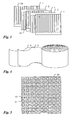
- Figure 3 shows the formation of an interposer according to the invention.
- Foils of sheets of a first type 1 and of a second type 2 are stacked in alternating order.
- Type 1 foils carry the metal structures 21, which extend to the top surface of the interposer and type 2 foils carry the metal structures 22, which extend towards the bottom surface of the interposer.
- the width of a metal structure plus the distance to the next metal structure on a foil is at least smaller than the pitch of the pins of the microchip to be attached. Preferably, this spacing is smaller than half the pitch of the microchip pins.
- Positioning of the interposer with respect to circuit board and microchip is hence not required since the inner metal structures cannot cause a shortcut in whatever arbitrary position.
- the pitch of the microchip pins can be 1 mm.
- the spacing of the metal structures is then chosen to 0,4 mm.
- the foils 1 and 2 can be made of polypropylene or polystyrene, for instance and good candidates for the material of the metal structures 21 and 22 are copper, silver, aluminum, or gold.
- the foils 1 and 2 are piled on a stack and then melted or glued together in a thermo-compression step. From the bulk pile thus formed, thin slices can be cut or sawed that build the interposer.
- the capacity that can be reached on the interposer by connecting these metal structures depends on the thickness of the foils and the surface area over which metal structures are connect and thus activated, but can be in the range of up to 20 nF.
- Figure 5 shows a horizontal cross-section through interposer 20.
- the grid of circles indicates the pitch of a BGA microchip and the horizontal rows of small stripes represent the vertical metal structures 21 and 22.
- Figure 6 shows a microscope photograph of a polished cut of the interposer 20, which shows the two types of metal structures 21 and 22.
- the interposer can alternatively be formed by growing ceramic layers between which the two sets of metal structures 21 and 22 are deposited and etched in alternating order. This is similar to the manufacturing of known ceramic capacitors, but that the metal layers between the ceramic layers are sub-structured according to the principle invention.
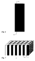
- the interposer is here constructed in a chessboard topology from capacitive elements C of the type shown in figure 6 including the vertical metal structures as described above and from conductive elements R, which serve as through-connections.
- the width d of the elements equals the pitch of the BGA pins of the microchip to be attached.
- top and bottom metal layers (not shown) allow the implementation of any circuit that might be required in a particular application.
- conductive elements R are provided only each second row in the chessboard topology.
Landscapes
- Engineering & Computer Science (AREA)
- Power Engineering (AREA)
- Microelectronics & Electronic Packaging (AREA)
- Manufacturing & Machinery (AREA)
- Physics & Mathematics (AREA)
- Electromagnetism (AREA)
- Production Of Multi-Layered Print Wiring Board (AREA)
- Structures For Mounting Electric Components On Printed Circuit Boards (AREA)
- Combinations Of Printed Boards (AREA)
- Structure Of Printed Boards (AREA)
Abstract
Description
- The present invention relates to the field of electronics and more particular to an interposer for use on a printed circuit board for decoupling integrated circuits.
- As the level of integration increases, the number of pins of a integrated circuit package that need to be connected to a circuit board becomes larger and larger. A well known packaging technique is called Ball Grid Array (BGA), which is a type of microchip connection methodology. A Ball Grid Array chip is a square package with solder balls on the underside for surface mounting. Use of BGA allows die package size to be reduced by allowing more surface area for attachment. Smaller packaging allows more components to be mounted on a module making greater densities available.
- On the other hand, the clock rate under which modern integrated circuits operate becomes higher and higher with every generation of microchips. A basic requirement for high speed operation is the availability of sufficient energy at each power pin of the integrated circuit. This decoupling is typically achieved by connecting capacitors to each power pin, which buffer the current source and supply the short term energy demand. These capacitors, however, consume surface area on the circuit board and hence limit the achievable integration density.
- It has also been proposed to place an interposer between a microchip and the printed circuit board. An interposer is realized as a small, thin printed circuit board, which contains buried components such as capacitors and resistors arranged in layers inside the interposer. A buried capacitors is realized using a thin metalized dielectric foil. Such laminates can achieve a capacity of 4-10 nF/in2. However, since the surface area and volume of the interposer is limited, the number and capacity of capacitors that can be buried for the decoupling of power pins is restricted.
- It is therefore an object of the present invention to provide an improved decoupling for microchips on circuit boards.
- These and other objects of the invention that appear below are achieved by an interposer for the decoupling of a microchip on a circuit board. The interposer contains on its upper and lower surfaces structured metal layers for attachment to the microchip and the circuit board, respectively. Inside the interposer, there are two sets of mutually isolated metal structures extending substantially perpendicular to the upper and lower surfaces of said interposer. The first set extends closer towards the upper surface than said second set, while the second set extends closer towards the lower surface than said first set.
- In this interposer, capacitors are easily formed by connecting metal structures from the first set to the top metal layer and adjacent metal structures from the second set to the bottom metal layer. This allows high capacities with very short connections for every pin. The new interposer is a standard base element that can be applied with high flexibility.
- Preferred embodiments of the invention will be described below with reference to the accompanying drawings, in which
- figure 1
- shows a first embodiment of a BGA microchip attached with an interposer on a circuit board;
- figure 2
- shows a second embodiment of a BGA microchip attached with an interposer on a circuit board;
- figure 3
- shows the construction of an interposer according to the invention;
- figure 4
- shows an alternative construction of an interposer according to the invention;
- figure 5
- shows a cross-section of an interposer compared to the pitch of a microchip;
- figure 6
- shows a polished cut image of an interposer according to the invention; and
- figure 7
- shows an implementation with additional through connections.
- A first embodiment of the invention is shown schematically as a cross-section in figure 1. A Ball Grid Array (BGA) packaged
microchip 10 is attached on aninterposer 20, which is fastened on a printedcircuit board 30. The microchip has threesolder balls corresponding solder pads Solder balls circuit board 30 connect tocorresponding solder pads interposer 20. - The
interposer 20 itself containsvertical metal structures metal structures 21 extends towards the top surface layer of theinterposer 20 and a second set ofmetal structures 22 extends towards the bottom surface of theinterposer 20.Solder pads upper metal structures 21, whilesolder pad 26f for instance connects to some of thelower metal structures 22.Solder pads blind vias solder balls respective metal structures solder pads area 29 serves as a capacitor betweensolder pads -
Blind vias - In this simplified example,
solder ball 12 is a power pin ofmicrochip 10 and is connected over through-connection 25 to apower supply point 32 on the circuit board.Solder ball 33 on the circuit board connects to ground level, so that thecapacitor 29 built by the metal structures betweenpads power pin 12. - Figure 2 shows a similar assembly but with the difference that instead of single top and bottom metal layers, additional
circuit board layers circuit board layers - Due to the extra
circuit board layers inner metal structures solder balls blind vias solder balls blind vias - Figure 3 shows the formation of an interposer according to the invention. Foils of sheets of a
first type 1 and of asecond type 2 are stacked in alternating order.Type 1 foils carry themetal structures 21, which extend to the top surface of the interposer andtype 2 foils carry themetal structures 22, which extend towards the bottom surface of the interposer. The width of a metal structure plus the distance to the next metal structure on a foil is at least smaller than the pitch of the pins of the microchip to be attached. Preferably, this spacing is smaller than half the pitch of the microchip pins. Positioning of the interposer with respect to circuit board and microchip is hence not required since the inner metal structures cannot cause a shortcut in whatever arbitrary position. As an example, the pitch of the microchip pins can be 1 mm. The spacing of the metal structures is then chosen to 0,4 mm. - The
foils metal structures - The
foils - The capacity that can be reached on the interposer by connecting these metal structures depends on the thickness of the foils and the surface area over which metal structures are connect and thus activated, but can be in the range of up to 20 nF.
- In figure 4, as an alternative, long widths of
foils - Figure 5 shows a horizontal cross-section through
interposer 20. The grid of circles indicates the pitch of a BGA microchip and the horizontal rows of small stripes represent thevertical metal structures - Figure 6 shows a microscope photograph of a polished cut of the
interposer 20, which shows the two types ofmetal structures - Rather than bonding layers of foils together, the interposer can alternatively be formed by growing ceramic layers between which the two sets of
metal structures - Another embodiment of the invention is shown in figure 7. The interposer is here constructed in a chessboard topology from capacitive elements C of the type shown in figure 6 including the vertical metal structures as described above and from conductive elements R, which serve as through-connections. The width d of the elements equals the pitch of the BGA pins of the microchip to be attached. Proper design of top and bottom metal layers (not shown) allow the implementation of any circuit that might be required in a particular application. Preferably, conductive elements R are provided only each second row in the chessboard topology.
- Having described specific embodiments of the present invention in full detail, it should be clear to those skilled in the art, that various modifications and changes can be made without departing from the concepts of the invention.
Claims (10)
- An interposer (20) for decoupling a microchip (10) on a circuit board (30), said interposer (20) comprises on its top and bottom surfaces structured metal layers (26a-f) for attachment to the microchip (10) and the circuit board (30), respectively,
characterized in that
said interposer (20) comprises internally two sets of mutually isolated metal structures (21, 22) extending substantially perpendicular to the upper and lower surfaces of the interposer (20), wherein said first set (21) extends closer towards the top surface than said second set (22) and said second set (22) extends closer towards the bottom surface than said first set (21). - An interposer according to claim 1, wherein the spacing between adjacent metal structures (21, 22) is less than half of the pitch of two connections of the microchip (10).
- An interposer according to claim 1, which is built from vertically joint foils (1, 2) carrying said metal structures (21, 22).
- An interposer according to claim 3, wherein said foils (1, 2) carry in alternating order said two sets of metal structures (21, 22), respectively.
- An interposer according to claim 1, wherein said interposer is built from a reel of two foils (1, 2) carrying said two sets of metal structures (21, 22), respectively.
- An interposer according to claim 1, wherein said interposer is built from vertical ceramic layers between which said two sets of metal structures (21, 22) are deposited in alternating order.
- An interposer according to claim 1, wherein said first set of metal structures (21) connects to the top metal layer (26a-c) and said second set of metal structures (22) connects to the bottom side metal layer (26d, 26f).
- An interposer according to claim 1, wherein the top metal layer is connectable to said first set of metal structures (21) by a blind via (24a) of a first depth and to said second set of metal structures (22) by a blind via (23a) of a second depth and wherein the bottom metal layer is connectable to said second set of metal structures (22) by a blind via (24b) of the first depth and to said first set of metal structures (21) by a blind via (23b) of the second depth.
- An interposer according to claim 1, comprising through connections (25, R) between said structured top and bottom metal layers.
- A circuit board (30) comprising at least one microchip (10) attached thereon, characterized in that between said circuit board (30) and said microchip (10) there is an interposer (20) according to any of the preceding claims.
Priority Applications (5)
| Application Number | Priority Date | Filing Date | Title |
|---|---|---|---|
| DE602005027534T DE602005027534D1 (en) | 2005-02-04 | 2005-02-04 | Interposer for decoupling of integrated circuits on a printed circuit board |
| EP05290242A EP1688995B1 (en) | 2005-02-04 | 2005-02-04 | Interposer for decoupling integrated circuits on a circuit board |
| AT05290242T ATE506697T1 (en) | 2005-02-04 | 2005-02-04 | INTERPOSER FOR DECOUPLING INTEGRATED CIRCUITS ON A PCB |
| US11/302,268 US7964802B2 (en) | 2005-02-04 | 2005-12-14 | Interposer for decoupling integrated circuits on a circuit board |
| CNB200510132977XA CN100405594C (en) | 2005-02-04 | 2005-12-29 | Interposer for IC decoupling on circuit boards |
Applications Claiming Priority (1)
| Application Number | Priority Date | Filing Date | Title |
|---|---|---|---|
| EP05290242A EP1688995B1 (en) | 2005-02-04 | 2005-02-04 | Interposer for decoupling integrated circuits on a circuit board |
Publications (2)
| Publication Number | Publication Date |
|---|---|
| EP1688995A1 true EP1688995A1 (en) | 2006-08-09 |
| EP1688995B1 EP1688995B1 (en) | 2011-04-20 |
Family
ID=34941928
Family Applications (1)
| Application Number | Title | Priority Date | Filing Date |
|---|---|---|---|
| EP05290242A Expired - Lifetime EP1688995B1 (en) | 2005-02-04 | 2005-02-04 | Interposer for decoupling integrated circuits on a circuit board |
Country Status (5)
| Country | Link |
|---|---|
| US (1) | US7964802B2 (en) |
| EP (1) | EP1688995B1 (en) |
| CN (1) | CN100405594C (en) |
| AT (1) | ATE506697T1 (en) |
| DE (1) | DE602005027534D1 (en) |
Cited By (4)
| Publication number | Priority date | Publication date | Assignee | Title |
|---|---|---|---|---|
| EP2115772A4 (en) * | 2007-02-12 | 2010-03-17 | Kemet Electronics Corp | PASSIVE ELECTRONIC DEVICE |
| WO2016073501A1 (en) * | 2014-11-05 | 2016-05-12 | Invensas Corporation | Substrates and methods of manufacture |
| US10083909B2 (en) | 2015-12-14 | 2018-09-25 | Invensas Corporation | Embedded vialess bridges |
| US10283492B2 (en) | 2015-06-23 | 2019-05-07 | Invensas Corporation | Laminated interposers and packages with embedded trace interconnects |
Families Citing this family (4)
| Publication number | Priority date | Publication date | Assignee | Title |
|---|---|---|---|---|
| US8723047B2 (en) * | 2007-03-23 | 2014-05-13 | Huawei Technologies Co., Ltd. | Printed circuit board, design method thereof and mainboard of terminal product |
| US9282646B2 (en) * | 2012-05-24 | 2016-03-08 | Unimicron Technology Corp. | Interposed substrate and manufacturing method thereof |
| JP6084475B2 (en) * | 2013-02-04 | 2017-02-22 | 株式会社神戸製鋼所 | Weld metal and welded structures |
| US10916493B2 (en) * | 2018-11-27 | 2021-02-09 | International Business Machines Corporation | Direct current blocking capacitors |
Citations (6)
| Publication number | Priority date | Publication date | Assignee | Title |
|---|---|---|---|---|
| FR2622346A1 (en) * | 1987-10-23 | 1989-04-28 | Eurofarad | Capacitor for electronic micro-circuit and arrangement incorporating such a capacitor |
| EP1100096A1 (en) * | 1999-04-23 | 2001-05-16 | Matsushita Electric Industrial Co., Ltd. | Electronic device and manufacture thereof |
| US6292351B1 (en) * | 1999-11-17 | 2001-09-18 | Tdk Corporation | Multilayer ceramic capacitor for three-dimensional mounting |
| US20020085336A1 (en) * | 2000-12-29 | 2002-07-04 | Paul Winer | High performance via capacitor and method for manufacturing same |
| US20040108587A1 (en) * | 2002-12-09 | 2004-06-10 | Chudzik Michael Patrick | High density chip carrier with integrated passive devices |
| US20040121266A1 (en) * | 2002-12-23 | 2004-06-24 | Samsung Electro-Mechanics Co., Ltd. | Printed circuit board with embedded capacitors therein, and process for manufacturing the same |
Family Cites Families (5)
| Publication number | Priority date | Publication date | Assignee | Title |
|---|---|---|---|---|
| US6512182B2 (en) * | 2001-03-12 | 2003-01-28 | Ngk Spark Plug Co., Ltd. | Wiring circuit board and method for producing same |
| US6791035B2 (en) * | 2002-02-21 | 2004-09-14 | Intel Corporation | Interposer to couple a microelectronic device package to a circuit board |
| US7463474B2 (en) * | 2002-04-15 | 2008-12-09 | Avx Corporation | System and method of plating ball grid array and isolation features for electronic components |
| US7068490B2 (en) * | 2004-04-16 | 2006-06-27 | Kemet Electronics Corporation | Thermal dissipating capacitor and electrical component comprising same |
| US7545623B2 (en) * | 2006-11-27 | 2009-06-09 | Kemet Electronics Corporation | Interposer decoupling array having reduced electrical shorts |
-
2005
- 2005-02-04 AT AT05290242T patent/ATE506697T1/en not_active IP Right Cessation
- 2005-02-04 DE DE602005027534T patent/DE602005027534D1/en not_active Expired - Lifetime
- 2005-02-04 EP EP05290242A patent/EP1688995B1/en not_active Expired - Lifetime
- 2005-12-14 US US11/302,268 patent/US7964802B2/en not_active Expired - Fee Related
- 2005-12-29 CN CNB200510132977XA patent/CN100405594C/en not_active Expired - Fee Related
Patent Citations (6)
| Publication number | Priority date | Publication date | Assignee | Title |
|---|---|---|---|---|
| FR2622346A1 (en) * | 1987-10-23 | 1989-04-28 | Eurofarad | Capacitor for electronic micro-circuit and arrangement incorporating such a capacitor |
| EP1100096A1 (en) * | 1999-04-23 | 2001-05-16 | Matsushita Electric Industrial Co., Ltd. | Electronic device and manufacture thereof |
| US6292351B1 (en) * | 1999-11-17 | 2001-09-18 | Tdk Corporation | Multilayer ceramic capacitor for three-dimensional mounting |
| US20020085336A1 (en) * | 2000-12-29 | 2002-07-04 | Paul Winer | High performance via capacitor and method for manufacturing same |
| US20040108587A1 (en) * | 2002-12-09 | 2004-06-10 | Chudzik Michael Patrick | High density chip carrier with integrated passive devices |
| US20040121266A1 (en) * | 2002-12-23 | 2004-06-24 | Samsung Electro-Mechanics Co., Ltd. | Printed circuit board with embedded capacitors therein, and process for manufacturing the same |
Cited By (10)
| Publication number | Priority date | Publication date | Assignee | Title |
|---|---|---|---|---|
| EP2115772A4 (en) * | 2007-02-12 | 2010-03-17 | Kemet Electronics Corp | PASSIVE ELECTRONIC DEVICE |
| WO2016073501A1 (en) * | 2014-11-05 | 2016-05-12 | Invensas Corporation | Substrates and methods of manufacture |
| US9583426B2 (en) | 2014-11-05 | 2017-02-28 | Invensas Corporation | Multi-layer substrates suitable for interconnection between circuit modules |
| US10014243B2 (en) | 2014-11-05 | 2018-07-03 | Invensas Corporation | Interconnection substrates for interconnection between circuit modules, and methods of manufacture |
| TWI670825B (en) * | 2014-11-05 | 2019-09-01 | Invensas Corporation | Substrates and methods of manufacture |
| US10586759B2 (en) | 2014-11-05 | 2020-03-10 | Invensas Corporation | Interconnection substrates for interconnection between circuit modules, and methods of manufacture |
| US10283492B2 (en) | 2015-06-23 | 2019-05-07 | Invensas Corporation | Laminated interposers and packages with embedded trace interconnects |
| US10636780B2 (en) | 2015-06-23 | 2020-04-28 | Invensas Corporation | Laminated interposers and packages with embedded trace interconnects |
| US10083909B2 (en) | 2015-12-14 | 2018-09-25 | Invensas Corporation | Embedded vialess bridges |
| US10347582B2 (en) | 2015-12-14 | 2019-07-09 | Invensas Corporation | Embedded vialess bridges |
Also Published As
| Publication number | Publication date |
|---|---|
| ATE506697T1 (en) | 2011-05-15 |
| CN1822356A (en) | 2006-08-23 |
| US7964802B2 (en) | 2011-06-21 |
| EP1688995B1 (en) | 2011-04-20 |
| CN100405594C (en) | 2008-07-23 |
| US20060176674A1 (en) | 2006-08-10 |
| DE602005027534D1 (en) | 2011-06-01 |
Similar Documents
| Publication | Publication Date | Title |
|---|---|---|
| US9743530B2 (en) | Chip capacitors | |
| JP5153099B2 (en) | Laminated structure of support plate with embedded semiconductor element | |
| US9978721B2 (en) | Apparatus for stacked semiconductor packages and methods of fabricating the same | |
| US9018040B2 (en) | Power distribution for 3D semiconductor package | |
| JP4912992B2 (en) | Capacitor-embedded substrate and manufacturing method thereof | |
| US20180315735A1 (en) | Embedded Organic Interposers for High Bandwidth | |
| KR101696705B1 (en) | Chip embedded type printed circuit board and method of manufacturing the same and stack package using the same | |
| KR102628536B1 (en) | semiconductor package having stacked chip structure | |
| CN101123854A (en) | Capacitor built-in substrate, manufacturing method thereof, and electronic device | |
| JP2004221583A (en) | Flex-based IC package structure using balanced lamination structure | |
| KR100920039B1 (en) | Multilayer semiconductor package and manufacturing method thereof | |
| JP2011023439A (en) | Capacitor and method of manufacturing the same | |
| JP2009252893A (en) | Semiconductor device | |
| US7964802B2 (en) | Interposer for decoupling integrated circuits on a circuit board | |
| US20080073797A1 (en) | Semiconductor die module and package and fabricating method of semiconductor package | |
| US20110271523A1 (en) | Ball grid array stack | |
| CN115064503A (en) | Three-dimensional stacking structure of radio frequency circuit and manufacturing method thereof | |
| KR101070022B1 (en) | Multi-layer ceramic circuit board, fabrication method of the same and electric device module | |
| US11219120B2 (en) | Stress relief opening for reducing warpage of component carriers | |
| JP6873147B2 (en) | 3D electronic module miniaturization Chip-on-chip interconnection method | |
| KR102146131B1 (en) | Device of package stacking | |
| KR101013560B1 (en) | Laminated Semiconductor Package and Method of Manufacturing the Same | |
| CN100552940C (en) | Stack structure of semiconductor element embedded loading board | |
| CN220627803U (en) | Semiconductor package structure and chip including same | |
| KR20100109040A (en) | Stacked semiconductor package and method of manufacturing the same |
Legal Events
| Date | Code | Title | Description |
|---|---|---|---|
| PUAI | Public reference made under article 153(3) epc to a published international application that has entered the european phase |
Free format text: ORIGINAL CODE: 0009012 |
|
| 17P | Request for examination filed |
Effective date: 20051013 |
|
| AK | Designated contracting states |
Kind code of ref document: A1 Designated state(s): AT BE BG CH CY CZ DE DK EE ES FI FR GB GR HU IE IS IT LI LT LU MC NL PL PT RO SE SI SK TR |
|
| AX | Request for extension of the european patent |
Extension state: AL BA HR LV MK YU |
|
| RAP1 | Party data changed (applicant data changed or rights of an application transferred) |
Owner name: ALCATEL LUCENT |
|
| AKX | Designation fees paid |
Designated state(s): AT BE BG CH CY CZ DE DK EE ES FI FR GB GR HU IE IS IT LI LT LU MC NL PL PT RO SE SI SK TR |
|
| 17Q | First examination report despatched |
Effective date: 20070807 |
|
| RIC1 | Information provided on ipc code assigned before grant |
Ipc: H01G 4/232 20060101ALI20100914BHEP Ipc: H01L 23/498 20060101AFI20100914BHEP Ipc: H01L 23/50 20060101ALI20100914BHEP Ipc: H05K 1/02 20060101ALI20100914BHEP Ipc: H05K 1/16 20060101ALN20100914BHEP |
|
| GRAP | Despatch of communication of intention to grant a patent |
Free format text: ORIGINAL CODE: EPIDOSNIGR1 |
|
| GRAS | Grant fee paid |
Free format text: ORIGINAL CODE: EPIDOSNIGR3 |
|
| GRAA | (expected) grant |
Free format text: ORIGINAL CODE: 0009210 |
|
| AK | Designated contracting states |
Kind code of ref document: B1 Designated state(s): AT BE BG CH CY CZ DE DK EE ES FI FR GB GR HU IE IS IT LI LT LU MC NL PL PT RO SE SI SK TR |
|
| REG | Reference to a national code |
Ref country code: GB Ref legal event code: FG4D |
|
| REG | Reference to a national code |
Ref country code: CH Ref legal event code: EP |
|
| REG | Reference to a national code |
Ref country code: IE Ref legal event code: FG4D |
|
| REF | Corresponds to: |
Ref document number: 602005027534 Country of ref document: DE Date of ref document: 20110601 Kind code of ref document: P |
|
| REG | Reference to a national code |
Ref country code: DE Ref legal event code: R096 Ref document number: 602005027534 Country of ref document: DE Effective date: 20110601 |
|
| REG | Reference to a national code |
Ref country code: NL Ref legal event code: VDEP Effective date: 20110420 |
|
| LTIE | Lt: invalidation of european patent or patent extension |
Effective date: 20110420 |
|
| PG25 | Lapsed in a contracting state [announced via postgrant information from national office to epo] |
Ref country code: SE Free format text: LAPSE BECAUSE OF FAILURE TO SUBMIT A TRANSLATION OF THE DESCRIPTION OR TO PAY THE FEE WITHIN THE PRESCRIBED TIME-LIMIT Effective date: 20110420 Ref country code: PT Free format text: LAPSE BECAUSE OF FAILURE TO SUBMIT A TRANSLATION OF THE DESCRIPTION OR TO PAY THE FEE WITHIN THE PRESCRIBED TIME-LIMIT Effective date: 20110822 Ref country code: LT Free format text: LAPSE BECAUSE OF FAILURE TO SUBMIT A TRANSLATION OF THE DESCRIPTION OR TO PAY THE FEE WITHIN THE PRESCRIBED TIME-LIMIT Effective date: 20110420 |
|
| PG25 | Lapsed in a contracting state [announced via postgrant information from national office to epo] |
Ref country code: BE Free format text: LAPSE BECAUSE OF FAILURE TO SUBMIT A TRANSLATION OF THE DESCRIPTION OR TO PAY THE FEE WITHIN THE PRESCRIBED TIME-LIMIT Effective date: 20110420 Ref country code: ES Free format text: LAPSE BECAUSE OF FAILURE TO SUBMIT A TRANSLATION OF THE DESCRIPTION OR TO PAY THE FEE WITHIN THE PRESCRIBED TIME-LIMIT Effective date: 20110731 Ref country code: IS Free format text: LAPSE BECAUSE OF FAILURE TO SUBMIT A TRANSLATION OF THE DESCRIPTION OR TO PAY THE FEE WITHIN THE PRESCRIBED TIME-LIMIT Effective date: 20110820 Ref country code: AT Free format text: LAPSE BECAUSE OF FAILURE TO SUBMIT A TRANSLATION OF THE DESCRIPTION OR TO PAY THE FEE WITHIN THE PRESCRIBED TIME-LIMIT Effective date: 20110420 Ref country code: FI Free format text: LAPSE BECAUSE OF FAILURE TO SUBMIT A TRANSLATION OF THE DESCRIPTION OR TO PAY THE FEE WITHIN THE PRESCRIBED TIME-LIMIT Effective date: 20110420 Ref country code: SI Free format text: LAPSE BECAUSE OF FAILURE TO SUBMIT A TRANSLATION OF THE DESCRIPTION OR TO PAY THE FEE WITHIN THE PRESCRIBED TIME-LIMIT Effective date: 20110420 Ref country code: CY Free format text: LAPSE BECAUSE OF FAILURE TO SUBMIT A TRANSLATION OF THE DESCRIPTION OR TO PAY THE FEE WITHIN THE PRESCRIBED TIME-LIMIT Effective date: 20110420 Ref country code: GR Free format text: LAPSE BECAUSE OF FAILURE TO SUBMIT A TRANSLATION OF THE DESCRIPTION OR TO PAY THE FEE WITHIN THE PRESCRIBED TIME-LIMIT Effective date: 20110721 |
|
| PG25 | Lapsed in a contracting state [announced via postgrant information from national office to epo] |
Ref country code: NL Free format text: LAPSE BECAUSE OF FAILURE TO SUBMIT A TRANSLATION OF THE DESCRIPTION OR TO PAY THE FEE WITHIN THE PRESCRIBED TIME-LIMIT Effective date: 20110420 |
|
| PG25 | Lapsed in a contracting state [announced via postgrant information from national office to epo] |
Ref country code: CZ Free format text: LAPSE BECAUSE OF FAILURE TO SUBMIT A TRANSLATION OF THE DESCRIPTION OR TO PAY THE FEE WITHIN THE PRESCRIBED TIME-LIMIT Effective date: 20110420 Ref country code: EE Free format text: LAPSE BECAUSE OF FAILURE TO SUBMIT A TRANSLATION OF THE DESCRIPTION OR TO PAY THE FEE WITHIN THE PRESCRIBED TIME-LIMIT Effective date: 20110420 |
|
| RAP2 | Party data changed (patent owner data changed or rights of a patent transferred) |
Owner name: ALCATEL LUCENT |
|
| PLBE | No opposition filed within time limit |
Free format text: ORIGINAL CODE: 0009261 |
|
| STAA | Information on the status of an ep patent application or granted ep patent |
Free format text: STATUS: NO OPPOSITION FILED WITHIN TIME LIMIT |
|
| PG25 | Lapsed in a contracting state [announced via postgrant information from national office to epo] |
Ref country code: RO Free format text: LAPSE BECAUSE OF FAILURE TO SUBMIT A TRANSLATION OF THE DESCRIPTION OR TO PAY THE FEE WITHIN THE PRESCRIBED TIME-LIMIT Effective date: 20110420 Ref country code: DK Free format text: LAPSE BECAUSE OF FAILURE TO SUBMIT A TRANSLATION OF THE DESCRIPTION OR TO PAY THE FEE WITHIN THE PRESCRIBED TIME-LIMIT Effective date: 20110420 Ref country code: SK Free format text: LAPSE BECAUSE OF FAILURE TO SUBMIT A TRANSLATION OF THE DESCRIPTION OR TO PAY THE FEE WITHIN THE PRESCRIBED TIME-LIMIT Effective date: 20110420 Ref country code: PL Free format text: LAPSE BECAUSE OF FAILURE TO SUBMIT A TRANSLATION OF THE DESCRIPTION OR TO PAY THE FEE WITHIN THE PRESCRIBED TIME-LIMIT Effective date: 20110420 |
|
| REG | Reference to a national code |
Ref country code: CH Ref legal event code: PCOW Free format text: ALCATEL LUCENT;3, AVENUE OCTAVE GREARD;75007 PARIS (FR) |
|
| 26N | No opposition filed |
Effective date: 20120123 |
|
| REG | Reference to a national code |
Ref country code: DE Ref legal event code: R097 Ref document number: 602005027534 Country of ref document: DE Effective date: 20120123 |
|
| PG25 | Lapsed in a contracting state [announced via postgrant information from national office to epo] |
Ref country code: IT Free format text: LAPSE BECAUSE OF FAILURE TO SUBMIT A TRANSLATION OF THE DESCRIPTION OR TO PAY THE FEE WITHIN THE PRESCRIBED TIME-LIMIT Effective date: 20110420 |
|
| PG25 | Lapsed in a contracting state [announced via postgrant information from national office to epo] |
Ref country code: MC Free format text: LAPSE BECAUSE OF NON-PAYMENT OF DUE FEES Effective date: 20120229 |
|
| REG | Reference to a national code |
Ref country code: CH Ref legal event code: PL |
|
| PG25 | Lapsed in a contracting state [announced via postgrant information from national office to epo] |
Ref country code: CH Free format text: LAPSE BECAUSE OF NON-PAYMENT OF DUE FEES Effective date: 20120229 Ref country code: LI Free format text: LAPSE BECAUSE OF NON-PAYMENT OF DUE FEES Effective date: 20120229 |
|
| REG | Reference to a national code |
Ref country code: IE Ref legal event code: MM4A |
|
| PG25 | Lapsed in a contracting state [announced via postgrant information from national office to epo] |
Ref country code: IE Free format text: LAPSE BECAUSE OF NON-PAYMENT OF DUE FEES Effective date: 20120204 |
|
| PG25 | Lapsed in a contracting state [announced via postgrant information from national office to epo] |
Ref country code: BG Free format text: LAPSE BECAUSE OF FAILURE TO SUBMIT A TRANSLATION OF THE DESCRIPTION OR TO PAY THE FEE WITHIN THE PRESCRIBED TIME-LIMIT Effective date: 20110720 |
|
| REG | Reference to a national code |
Ref country code: FR Ref legal event code: GC Effective date: 20131018 |
|
| PG25 | Lapsed in a contracting state [announced via postgrant information from national office to epo] |
Ref country code: TR Free format text: LAPSE BECAUSE OF FAILURE TO SUBMIT A TRANSLATION OF THE DESCRIPTION OR TO PAY THE FEE WITHIN THE PRESCRIBED TIME-LIMIT Effective date: 20110420 |
|
| PG25 | Lapsed in a contracting state [announced via postgrant information from national office to epo] |
Ref country code: LU Free format text: LAPSE BECAUSE OF NON-PAYMENT OF DUE FEES Effective date: 20120204 |
|
| PG25 | Lapsed in a contracting state [announced via postgrant information from national office to epo] |
Ref country code: HU Free format text: LAPSE BECAUSE OF FAILURE TO SUBMIT A TRANSLATION OF THE DESCRIPTION OR TO PAY THE FEE WITHIN THE PRESCRIBED TIME-LIMIT Effective date: 20050204 |
|
| REG | Reference to a national code |
Ref country code: FR Ref legal event code: RG Effective date: 20141016 |
|
| REG | Reference to a national code |
Ref country code: FR Ref legal event code: PLFP Year of fee payment: 11 |
|
| REG | Reference to a national code |
Ref country code: FR Ref legal event code: PLFP Year of fee payment: 12 |
|
| REG | Reference to a national code |
Ref country code: FR Ref legal event code: PLFP Year of fee payment: 13 |
|
| REG | Reference to a national code |
Ref country code: FR Ref legal event code: PLFP Year of fee payment: 14 |
|
| PGFP | Annual fee paid to national office [announced via postgrant information from national office to epo] |
Ref country code: DE Payment date: 20190122 Year of fee payment: 15 Ref country code: FR Payment date: 20190111 Year of fee payment: 15 Ref country code: GB Payment date: 20190130 Year of fee payment: 15 |
|
| REG | Reference to a national code |
Ref country code: DE Ref legal event code: R119 Ref document number: 602005027534 Country of ref document: DE |
|
| GBPC | Gb: european patent ceased through non-payment of renewal fee |
Effective date: 20200204 |
|
| PG25 | Lapsed in a contracting state [announced via postgrant information from national office to epo] |
Ref country code: GB Free format text: LAPSE BECAUSE OF NON-PAYMENT OF DUE FEES Effective date: 20200204 Ref country code: FR Free format text: LAPSE BECAUSE OF NON-PAYMENT OF DUE FEES Effective date: 20200229 Ref country code: DE Free format text: LAPSE BECAUSE OF NON-PAYMENT OF DUE FEES Effective date: 20200901 |